Embed Size (px)
Citation preview

Silicon Surface Modification and Characterization for EmergentPhotovoltaic Applications Based on Energy TransferWeina Peng,† Sara M. Rupich,† Natis Shafiq,† Yuri N. Gartstein,‡ Anton V. Malko,*,†,‡
and Yves J. Chabal*,†
†Department of Materials Science and Engineering and ‡Department of Physics, University of Texas at Dallas, Richardson, Texas75080, United States
CONTENTS
1. Introduction 127642. Chemical Modification of Silicon Surfaces: Oxi-
dized vs Oxide-Free Surfaces 127652.1. Background 127652.2. Formation of H-Terminated Silicon Surfaces 127652.3. Stability of H-Terminated Silicon Surfaces 127662.4. Structural Modification of Silicon Surfaces 12766
3. Functionalization of Oxide-Free Silicon Surfaces 127673.1. Background 127673.2. Hydrosilylation of H-Terminated Surfaces 12767
3.2.1. Background 127673.2.2. Catalyst-Aided Reactions 127673.2.3. Photochemically Induced Reactions 127683.2.4. Thermally Activated Reactions 12769
4. Selected Techniques for Characterizing WetChemically Functionalized Surfaces 127694.1. Infrared Absorption Spectroscopy 127704.2. X-ray Photoelectron Spectroscopy 127704.3. Capacitance−Voltage and Conductance−
Voltage Measurements 127714.4. Surface Recombination Velocity Measure-
ments 127725. Deposition of Nanocrystal Quantum Dots on
Silicon Surfaces 127735.1. Grafting of Nanocrystal Quantum Dots to
Functionalized Surfaces 127735.2. Layer-by-Layer Assembly 127745.3. Self-Assembly of Nanocrystal Quantum Dot
Monolayers at the Air−Liquid Interface 127756. Energy Transfer Mechanisms from Nanocrystal
Quantum Dots to Silicon 127766.1. Theoretical Considerations 127766.2. Determination of NRET Efficiencies from
Nanocrystal Quantum Dots to Semiconduc-tor Substrates 12778
6.3. Energy Transfer in Nanocrystal Quantum DotSolids on Silicon 12779
6.4. Radiative Energy Transfer to Silicon Sub-strates 12780
6.5. Nanocrystal Quantum Dot Sensitization ofNanostructured Silicon Substrates 12781
6.6. Multiexciton Generation and Singlet ExcitonFission in Applications to Silicon Sensitization 12782
7. Electrical Measurements of Quantum-Dot-Modi-fied Silicon Nanostructures 127837.1. Direct Photocurrent Measurements 127837.2. Time Resolved Photocurrent Measurements 12784
8. Summary and Outlook 12785Author Information 12786
Corresponding Authors 12786Author Contributions 12786Author Contributions 12786Notes 12786Biographies 12786
Acknowledgments 12788References 12788
1. INTRODUCTION
Sensitization of crystalline silicon and other semiconductors bymeans of energy transfer (ET) may facilitate their utilization inthin-film flexible solar cells and is also interesting in the generalcontext of hybrid nanostructures. ET-based hybrid nanostruc-tures constitute a class of systems that can potentially offer aversatile platform for various optoelectronic applications.1−3 Inhybrid systems, the optical and electrical functionalities areclearly separated: one component of the system has strongoptical absorption while the other possesses good electricaltransport. Importantly, the “coupling” of these components isenabled by a near-f ield electromagnetic interaction that leads tothe interconversion of excitons and electron−hole pairs. In thephotovoltaic (PV) mode of operation, sunlight is initiallyharvested in the highly absorbing component of the hybrid,creating an exciton. Then energy transfer across the interface (nocharge transfer required) enables creation of electron−hole pairsin the high-mobility semiconductor substrate, where chargeseparation and transport take place. The separation offunctionalities in hybrid systems is similar to photosynthesis,4
Special Issue: Solar Energy Conversion
Received: February 6, 2015Published: August 5, 2015
Review
pubs.acs.org/CR
© 2015 American Chemical Society 12764 DOI: 10.1021/acs.chemrev.5b00085Chem. Rev. 2015, 115, 12764−12796

where photons are absorbed in light-harvesting complexes andthen funneled to reaction centers, where charge separationoccurs. As a result, hybrid systems that employ energy transferprinciples are conceptually different from the more commonphotovoltaic architectures operating via charge separation andtransport principles.5,6 Exciton dissociation at the interfaceresults in separated charge carriers; however, as both electronsand holes need to be transported to their respective electrodes viapercolating conductive networks, high carrier mobilities andefficiencies are required. In contrast, in ET-based structures,some of these demands can be relaxed. In particular, the ET routeappears to be attractive in regard to silicon nanostructures, wherethis approach could make it possible to utilize ultrathin Si layers7
as the high-mobility component which existing silicontechnologies are built upon. Indeed, the issue of weak absorptionin indirect band gap Si would no longer be a defining factor in thedetermination of the PV device thickness if the thin Si films areeffectively sensitized via ET from the strongly absorbingcomponent. More broadly, the strongly absorbing componentsof semiconducting ET hybrid nanostructures can be imagined tobe used in conjunction with material systems and geometricalarrangements, realizing the ideas of the third-generationphotovoltaics8,9 (multiple-carrier generation, up- and down-conversion, etc.) or luminescent solar concentrators.10,11 Whilethe feasibility of practical hybrid PV devices operating on ETprinciples is not established yet, the hope associated with thisconcept is well conveyed by the expressions “a new solar cellparadigm”12 and “the road to hybrid photovoltaics”13 used in thetitles of two papers on ET from nanocrystal quantum dots(NQDs) into silicon.To achieve ET-based structures, a number of issues have to be
addressed, as exemplified in this review with extensive coverageof crystalline silicon structures. The review is organized asfollows. Two sections focus on the chemical passivation,modification, and functionalization of the silicon substrate itself(sections 2 and 3), which are also relevant for properly graftingand depositing quantum dots. The modification also includes theformation of nanostructures to increase the overall surface area(section 2.4). The next section highlights the main techniquesused to characterize surfaces during the modification processes(section 4). A separate section is devoted to the deposition ofNQDs on a variety of modified surfaces (section 5), before thefundamentals of energy transfer are addressed, on the basis ofphotoluminescence measurements (section 6). The final sectionis focused on electrical measurements of NQD-modifiedsurfaces, with an emphasis on the fundamental mechanismsrather than device performance (section 7). Finally, a perspectiveis given as to the future directions in this field (section 8).
2. CHEMICAL MODIFICATION OF SILICON SURFACES:OXIDIZED VS OXIDE-FREE SURFACES
2.1. Background
There is already a wealth of information on the wet chemicalcleaning of Si for semiconductor processing,14,15 but there is lesson subsequent modification methods for sensitive applications,such as silicon photovoltaic devices, which is the focus of thisreview. Wet chemical functionalization is attractive, as it can beperformed in standard laboratories, is scalable, and usescommercially available chemicals. In general, wet chemicalprocessing is easier and more adaptable than chemicalmodification in either vapor-phase or ultrahigh vacuum (UHV)
environments and, in some cases, can also lead to surfaces withhigher structural and chemical uniformity.16−21
The importance of silicon as a substrate is due primarily to itsoxide, which is stable and forms an interface with silicon that ismuch better than any other semiconductor/oxide interface (e.g.,germanium/oxide).22 Surface functionalization of silicon hastherefore initially focused on functionalizing OH-terminatedsilicon oxide surfaces, using silanization with molecules such astriethoxysilanes or trichlorosilanes.23,24 There are, however,several issues associated with silicon oxide functionalization. Theprocess strongly depends on the density of initial surfacehydroxyl groups, the number of water molecules present, and thetemperature.25 Additionally, silane molecules frequently poly-merize, thus hindering the formation of a single self-assembledmonolayer (SAM), especially for short molecules (e.g., amino-propyltriethoxysilane). Alternatively, phosphonates can be used,as they are not water sensitive and can be attached to native oxidesurfaces under ambient conditions,26−29 although the layers areoften not well-defined.14,17−19 For both silane and phosphonatelayers, the surfaces are not stable in humid environments,particularly in high-pH liquids required for biological applica-tions. Despite these serious issues, the electrical quality of theinitial Si/SiO2 interface has motivated the functionalization ofoxides with silanes30−33 or phosphonates34 for the fabrication ofmost chemical sensors.For grafting NQDs onto silicon for PV cell applications, the
main requirements are (1) the density of electronic defect statesat the Si surface should be low (<1012/cm2), a common need forall electronic devices; (2) the distance of the NQDs to the siliconsubstrate should be as small as possible; and (3) the Si/organicinterface should be stable in humid environments. For thesereasons, we consider here oxide-free surfaces that, as we willshow, can be functionalized to satisfy the above requirements.For silicon, hydrogen and halogens have been considered for
the initial termination of oxide-free surfaces prior to function-alization, as they can be obtained via straightforward wetchemical processing (HF or PCl5 solutions). The next sectiondescribes, for instance, how hydrogen-terminated silicon surfacescan be formed in some detail.
2.2. Formation of H-Terminated Silicon Surfaces
Figure 1 summarizes the essential mechanism of hydrogentermination upon HF etching. In this mechanism, removal of thelast oxygen atom in the SiO2 overlayer leads to the formation ofSi−F. However, while this bond is especially strong (∼5 eV), it isalso highly polar. The strong static charge polarizes the Si−Siback-bond of SiSi−F, making it vulnerable to attack by HF, as
Figure 1. Mechanism leading to the formation of H-terminated siliconsurface by HF etching: The last step of oxygen removal from SiO2involves HF attack on the Si−O bond, with removal of OH as H2O andtermination of the surface Si atom with fluorine. Further attack of thepolarized Siδ−−Siδ+ bond leads to H termination. Reprinted withpermission from ref 40. Copyright 2012 John Wiley & Sons.
Chemical Reviews Review
DOI: 10.1021/acs.chemrev.5b00085Chem. Rev. 2015, 115, 12764−12796
12765

originally pointed out by Ubara et al.35 in the case ofmicrocrystalline Si.36 Calculations by Trucks et al.17 found thatthere is only an∼1 eV barrier to attach H to the back Si of SiSi−Fand release surface Si as SiF4. The resulting H-terminated siliconsurface is nonpolar and therefore highly resistant to chemicalattack by HF (i.e., no additional etching occurs), even though theSi−H bond energy is only ∼3.5 eV (i.e., lower than the Si−Fbond energy). Therefore, the surface is terminated by hydrogenatoms, not fluorine atoms,37,38 and the H-termination isresponsible for the resulting hydrophobicity, chemical resistance,and low density of electronic states (i.e., low recombinationvelocity) of the surface.39
After the Si surface is H-terminated, further etching can takeplace in heavily buf fered HF solutions (pH ∼8).16 In solutionssuch as NH4F, the presence of OH− ions or related speciesfosters additional oxidation of Si−Si bonds, allowing for slow andselective removal of Si atoms.18,20,21,41,42 The selectivity isassociated with surface structure: adstructures and steps areattacked more efficiently, leading to (i) atomically flat andperfectly monohydride-terminated Si(111) surfaces on well-oriented ⟨111⟩ Si surfaces, (ii) atomically straight and H-terminated steps on vicinal ⟨111⟩ Si surfaces,21,42 and (iii) quasi-atomically flat surfaces (with a double layer structure) on ⟨100⟩Si surfaces.43 For instance, a site-specific reaction model20
resulting in step flow etching has been suggested for theformation of atomically flat, monohydride-terminated surfaces.In summary, silicon can be hydrogen-terminated by immersionin concentrated or mildly diluted HF solutions. When bufferedHF solutions are used instead, care must be taken during etchingof highly structured or structurally patterned (e.g., nanopillared)surfaces because preferential etching can substantially change themorphology of the nanopatterns.
2.3. Stability of H-Terminated Silicon Surfaces
For NQD attachment on Si, functionalization of oxide-freesilicon surfaces requires a good understanding of the stability andselective reactivity of H-terminated Si surfaces. Despite theirrelatively good stability, H-terminated Si surfaces tend to degradein air. For instance, early studies showed that their surfacerecombination velocity decreased by an order of magnitude afterSi samples were removed from HF solution.39 Additionally, aftera few hours in air, some initial oxidation is often observed,although H-terminated Si surfaces remain stable in pure O2,H2O, and N2 gases,
14,44,45 with initial reaction at the steps (e.g.,with O2, NH3, and H2O) only at temperatures above 300°C.46−48 Consequently, it is believed that degradation in air isdue to reactive species (i.e., radicals, ozone) that react with Si−H,leaving the surface susceptible to oxidation.Understanding the surface stability in solution is challenging,
as solvation and proximity effects can decrease reaction barrierscompared to the gas phase, and electrochemical effects arepossible.In summary, the stability of H-terminated Si surfaces depends
critically on their environment, which needs to be consideredappropriately.
2.4. Structural Modification of Silicon Surfaces
Structural modification of silicon surfaces is an area of intenseinterest in the photovoltaic community. Patterned and nano-structured substrates have been considered for next-generationphotovoltaic applications49 due to their unique electrical,50−52
optical,53−55 thermal,56 electrochemical,57 and mechanical58
properties. For instance, solar cells composed of nanowire(NW) arrays can be manufactured simply and inexpensively, yet
they provide increased surface area and enhanced light collectioncompared to their planar analogs, as seen in Figure 2.53,59 In this
light, much work has been carried out on the formation andcharacterization of semiconductor nanostructures, such as NWsand nanopillars (NPs). It is believed that nanostructuredarchitectures can reduce the quantity of the materials requiredand open up the possibility to incorporate materials with lowercrystalline quality.Si NWs and NPs are fabricated via either bottom-up or top-
down approaches, and a number of reviews54,60−64 havediscussed these growth mechanisms.50,65−67 For bottom-upapproaches, vapor−liquid−solid (VLS) growth,66,68,69 oxide-assisted growth,70,71 and supercritical-fluid and solution growthare utilized.72,73 For top-down methods, a nanometer-sizepattern is first created, using methods such as electron beamlithography,51,74 nanoimprint lithography,75,76 nanosphereassembly,53,77−85 colloidal lithography,84,85 anodic alumina,86,87
or block copolymer formation,88−90 and then etched via deepreactive ion etching (DRIE) or metal-assisted chemical etching(MACE).53,91−97
Once the nanostructures are fabricated, significant efforts havefocused on characterization of their optical properties,55,59,98−101
specifically working to reduce reflection and improve lightabsorption and charge collection.52,53,55,92,99,100,102 Additionally,solar cell device performance,52,103,104 for both single SiNWs51,102,105−107 and arrays of Si NWs and NPs,100,108,109 hasbeen evaluated. It was found that carrier collection efficienciescan be improved in NW- and NP-based devices by incorporatingradial p−i−n junctions, where the direction of light absorptionand subsequent collection of photogenerated charge can bedecoupled.52 Such structures are useful because they make itpossible to explore fundamental issues that are important to
Figure 2. Cross-sectional SEM images of NW arrays (a) 2 μm and (b) 5μm in length. Scale bars are 10 μm. (c) Transmission spectra of arrays of2 μm (green) and 5 μm (black) long nanowires fabricated on 7.5 μmthick silicon. A large intensity reduction is observed through a red-shiftin the transmitted light after nanowire fabrication, which indicatesenhanced light trapping. Reprinted with permission from ref 53.Copyright 2010, American Chemical Society.
Chemical Reviews Review
DOI: 10.1021/acs.chemrev.5b00085Chem. Rev. 2015, 115, 12764−12796
12766

optimize devices. For instance, work has been done to passivatethe surfaces and interfaces as to minimize interfacial and surfacerecombination centers,51,110−116 which lower the overall deviceperformance. Control of the core and shell doping levels was alsofound to be necessary to ensure good PV performance andminimize charge recombination in the depletion region.52,117,118
Clearly, nanostructures still need improvement to achieveperformances similar to those of planar crystalline solarcells,53,106,107,116,119,120 but in the context of this review, theyare useful examples to highlight the value of surfacefunctionalization, which enables a more uniform attachment ofNQDs.
3. FUNCTIONALIZATION OF OXIDE-FREE SILICONSURFACES
3.1. Background
Functionalization of oxide-free silicon surfaces is a central part ofthe processing for energy transfer applications, such as NQD-enhanced silicon photovoltaic cells, because it makes it possibleto construct the most efficient structures. A number of excellentreviews focusing on the organic modification of H-terminated Sisurfaces have been written in the past decade,121−128 amongwhich only those addressing flat silicon surfaces122,124,127 arerelevant for energy transfer applications. Consequently, thereaction of the Si−H bond itself is relevant. We focus onhydrosilylation (based on alkene molecules) because it is a usefulmethod for replacing surface hydrogen a covalently bondedmolecule and forming a strong Si−C bond in the process. Analternative approach pioneered by Lewis et al. utilizeshalogenation of H-terminated Si surfaces, followed by theGrignard reaction.129 Specifically, H−Si(111) was converted toCl−Si(111) by immersion in PCl5 in chlorobenzene withbenzoyl peroxide as the radical initiator. Cl−Si(111) was inturn alkylated using alkyl−Li or other alkyl-Grignard reagents.This two-step method has been shown to produce high-qualitysurfaces and has been extensively investigated,129−134 as itprovided a means to functionalize previously inaccessiblesurfaces.135 After the initial demonstration, different methodsand reaction conditions were explored for both the halogenationand alkylation steps. For example, gas-phase halogenation of H−Si(111) has been achieved with Cl2(g) and Br2(g),
132,136,137
where the choice of solvent and its purity have been shown toaffect the degree of bond formation other than Si−C during thealkylation step.131,134 In addition to the primary literature, asignificant body of work exists that describes and contextualizesthe synthesis and properties of alkylated Si surfaces formed byhalogenation then alkylation of H−Si.126,138,139 In this review, wewill not discuss it further, because it has not yet been used toattach NQDs to Si surfaces, but it should be kept in mind as avaluable alternative to functionalize stable, oxide-free Si surfaces.Rather, we will focus on the different methods to create Si−Cbonds via hydrosilylation reactions.3.2. Hydrosilylation of H-Terminated Surfaces
3.2.1. Background. Hydrosilylation is a simple additionreaction of organic silicon hydrides compounds to unsaturatedcarbon molecules, such as CC, CO, or CN.140−142 It canbe facilitated with a catalyst or fostered by light or heat asschematically summarized in eq 1:
− + −
⎯ →⎯⎯⎯⎯⎯⎯⎯⎯⎯⎯⎯⎯⎯ − − −ν
Si H H C CH R
Si CH CH Rh
2catalyst, ,heat
2 2 (1)
Through any fabrication method, hydrosilylation results in theformation of a SAM where an alkyl chain is bound to the siliconsurface via a strong, nonpolar Si−C bond. This SAM isthermodynamically and kinetically stable.Among the three main forms of activation on surfaces
mentioned above, catalysis is particularly effective for homoge-neous hydrosilylation in solution, since the catalyst can easily beintroduced (and later removed). In this mechanism, the catalystserves to activate a double (or triple) bond. In optically orthermally activated hydrosilylation reactions, surface reactionsare involved that can be carried out via standard wet chemicalprocedures. These two methods work by creating energeticphotons or phonons, which form radicals either at the surface bybreaking the Si−H bond or on the alkene/alkyne by breaking thedouble/triple bond. Compared to catalytically driven reactions,the surface reactions depend on sterics, local surface structure,and the chemical nature of the surface bonds, i.e., kinetic barriers,rather than thermodynamics. Therefore, differences are expectedbetween crystallographic planes and complex nanostructures.After a brief review of catalyst-mediated reactions, we examine
optically and thermally activated reactions of alkenes with H-terminated silicon surfaces. For wet chemical processing, thealkenes or alkynes must be liquid, not degrade under elevatedtemperature or UV light, and only have one end group (thedouble/triple bond) reactive toward the substrate. In the case ofNQD grafting (which requires a bifunctional molecule), the useof a second nonreactive functional group, such as an ester, isneeded, where the ester can be deprotected and transformedafter attachment to the silicon surface. Importantly, all furthermodifications of themoleculemust not degrade the initial Si/SAMinterface.
3.2.2. Catalyst-Aided Reactions. Catalytically drivenreactions often take place in homogeneous media (solution).The catalyst drives the reaction by creating a radical140 orpolarizing the unsaturated bond (dominant mechanism for mostsystems). Frequently used catalysts include transition-metalcomplexes, nucleophiles (e.g, tertiary amine), or Lewis acids(AlCl3, EtAlCl2).
143−145 In 1965, Chalk and Harrod firstproposed a mechanism using transition-metal complexes ascatalysts for hydrosilylation, as shown in Figure 3,143 and this waslater expanded to EtAlCl2 (Figure 4) and peroxides (Figure 5).
Similar reactions were carried out on both H-terminated flatsilicon and porous silicon surfaces using palladium-, rhodium- orplatinum-based catalysts; however, this frequently resulted inoxidation and metal reduction, as discussed by Buriak125 andBoukherroub and Szunerits.121 For porous silicon, Lewis acid-catalyzed or -mediated hydrosilylation is the favored method.EtAlCl2 (a commonly used catalyst) was extensively used by
Figure 3. Mechanism proposed by Chalk and Harrod for thehydrosilylation of olefins catalyzed by group VIII metal complexes.Reprinted with permission from ref 143. Copyright 1965 AmericanChemical Society.
Chemical Reviews Review
DOI: 10.1021/acs.chemrev.5b00085Chem. Rev. 2015, 115, 12764−12796
12767

Boukkerroub et al.146 and Webb et al.147 on porous and flatsilicon surfaces. The mechanism is illustrated in Figure 4.144
Another route utilizes radical initiators, such as diacylperoxides, to functionalize H-terminated Si surfaces, as shownin Figure 5.148 This catalyst causes a self-propagating chainreaction on the surface in which radicals are formed andconsumed. A number of reports have examined, quantified, andconfirmed the kinetics related to this reaction using first-principlecalculations.149,150
Another method is hydrosilylation initiated by hydrideabstraction using compounds such as triphenylcarbeniumcations (Figure 6).151 In this case, a positively charged siliconsurface is created after the cation removes H−, which in turnenables a nucleophilic attack by the CC double bond(electron-rich). This results in Si−C bond formation and
creation of a new β-silyl-substituted carbocation, which thenpropagates the reaction.Of particular note for NQD grafting is a recent process by
Bowden and colleagues that used 4-(decanoate)-2,2,6,6-tetramethylpiperidinooxy (TEMPO) as a radical initiator.152
They showed that it was possible to graft both simple alkenes,such as 1-octadecene,152 or bifunctional molecules, such ascarboxylic acid-terminated alkenes, on silicon surfaces.153 Thisapproach enables the direct formation of SAMs with functionalgroups directly on silicon surfaces without further processing.
3.2.3. Photochemically Induced Reactions. For theapplications at hand, photoactivation is a practical method tofunctionalize H-terminated surfaces, as it is easily implemented.The process was initially believed to require photons with energygreater than the Si−H bond energy (∼3.5 eV or λ < 350 nm) inorder to break the Si−H bond, create a silicon radical, andactivate the silicon surface. Since silicon radicals react with water,creating silicon oxide, truly anhydrous alkene solutions arerequired. This idea motivated Chidsey and co-workers, whodemonstrated using X-ray photoelectron spectroscopy (XPS)that alkyl SAMs can be formed under UV illumination (Hg lamp,λ = 185 and 253.7 nm) for 2 h on Si−H surfaces immersed inpentene.135 This technique was extended to other alkene andalkyne molecules and different wavelengths, although it wasfound that oxidation could occur at λ < 350 nm if oxygen waspresent.154 These findings supported the hypothesis that shortUV radiation breaks the Si−H bond, creating a surface radicalthat could react either with an oxidizing species, resulting inoxidation, or with an unsaturated C−C bond, leading to acovalent Si−C bond. For isolated Si−H (e.g., H-terminatedsurfaces in a vacuum), the probability of Si−H bond dissociationis very small (>1011 photon per event) due to the low crosssection (i.e., one/number of photons).Photochemical grafting of alkenes has been successfully carried
out using a broad range of energies,155−158 including energiesboth higher and lower than 3.5 eV. Since hydrosilylation is stillsuccessful even when the photon energy is less than the energyneeded for homolytic bond cleavage, alternate mechanisms wereproposed where photoexcitation of substrate charges maygenerate active sites.155,156,158 In 2001, Stewart and Buriakproposed a wavelength-dependent mechanism where excitonsare generated in the substrate, which can then initiate thereaction.159 These two mechanisms are shown in Figure 7.The electron−hole pair mechanism was validated by grafting
alkenes on either oxide-free Si surfaces or oxidized surfaces, asillustrated in Figure 8. It was found that hydrosilylation onlyoccurred on H-terminated silicon surfaces, suggesting that the
Figure 4. Schematic representation of the hydrosilylation mechanismusing EtAlCl2 to catalyze the organosilicon reaction. Reprinted withpermission from ref 40. Copyright 2012 John Wiley & Sons.
Figure 5. Schematic representation of the hydrosilylation mechanismusing a peroxide agent to initiate a radical reaction. Reprinted withpermission from ref 40. Copyright 2012 John Wiley & Sons.
Figure 6. Schematic representation of the hydrosilylation mechanismusing a carbocation to initiate an ionic reaction. Reprinted withpermission from ref 40. Copyright 2012 John Wiley & Sons.
Figure 7. Schematic illustration of the two pathways for photochemi-cally induced reactions for hydrosilylation of H-terminated Si surfaces:(top) radical-based mechanism and (bottom) exciton-based mecha-nism. Reprinted with permission from ref 40. Copyright 2012 JohnWiley & Sons.
Chemical Reviews Review
DOI: 10.1021/acs.chemrev.5b00085Chem. Rev. 2015, 115, 12764−12796
12768

generation of electron−hole pairs is needed for UV-drivengrafting.160 Even if hydrosilylation is driven by excitonicprocesses, propagation of the reaction may still involve radicals.Hamers and colleagues proposed an alternate mechanism after
studying UV-initiated hydrosilylation on H-terminated diamondand amorphous carbon.161,162 In this study, successful grafting ondiamond under illumination with 254 nm light (photon energylower than the band gap)161 revealed that the exciton model maynot always be the dominant mechanism. Rather, it was suggestedthat radicals could be produced on the alkenes by photoemissionof electrons from the substrate into the alkene solution and thatthese molecules could then catalyze hydrosilylation on thecarbon surfaces. The same mechanism was also proposed forsilicon surfaces;162 however, definite confirmation is challengingto obtain.Whatever the mechanism, UV-induced hydrosilylation
provides a number of benefits. First, it enables grafting of alkenemolecules with different functional head groups, as surfaceradicals favor reaction with double bonds over molecules withunsaturated C−C bonds,163 including esters,164 activatedesters,165 and carboxylic acids.166 Additionally, the method iscompatible with optical lithography to fabricate patternedSAMs.167−169
For thoroughness, it is important to mention that photo-chemically initiated hydrosilylation reactions have successfullyfunctionalized other semiconductor substrates, such as GaN.170
3.2.4. Thermally Activated Reactions. For thermallyactivated hydrosilylation reactions, H-terminated Si surfacesare placed in an anhydrous alkene solution for hours to days atmoderately elevated temperatures (150−200 °C). In thisreaction, the alkene reacts directly with the Si−H, releasing H2and forming Si−C (Figure 9, bottom route). A benefit to thismethod is that the elevated reaction temperature enablesevaporation of residual water in the solution, decreasing therisk of surface oxidation.Through careful processing, high-quality
surfaces with minimal interfacial oxide and high photo-luminescence (PL) intensities (similar to H-terminated Sisurfaces) can be obtained.171−173 The alkyl-SAM-passivatedsurfaces are more stable than H-terminated silicon, even thoughthe alkene molecules replace <50% of the surface hydrogen.Since thermal hydrosilylation reactions were first carried out in
the early 1990s by Chidsey and co-workers,148,174 improvementsin the approach and resulting SAM quality have been achieved bySieval et al.175,176 Initially, these reactions were thought to followsimilar pathways to those initiated by catalysts or photochemicalactivation, where surface radicals were generated by UV light (λ <350 nm).125,177 It was believed that trace impurities (i.e., water,oxygen) initiated the reaction;177,178 however, doubts existed onwhether the Si−H bond (bond energies on the order of 80−90kcal mol−1) could be homolytically cleaved at 150 °C. A moreconcerted mechanism was therefore proposed121 and verified byDFT calculations, as illustrated in Figure 9.179
While the discussion above focused on alkenes, much work hasalso been carried out on the thermal activation of alkynes, and anumber of differences have been found. For instance, alkynes aremore reactive than alkenes. When a mixed alkene/alkynesolution or a bifunctional alkene- and alkyne-containingmolecule is used, the triple bond reacts instead of the doublebond.180 Additionally, Scheres et al. found that higher surfacecoverage is obtained for alkenyl SAMs than alkyl SAMs.181 Theincreased reactivity of alkynes allows the hydrosilylation reactionto occur under very mild conditions (room temperature) in thedark,182 while producing higher-quality surfaces than obtainedwith alkenes.183
Concerns that elevated temperatures may activate functionalgroups and enable side reactions with the Si−H surface havelimited the widespread use of thermally activated hydrosilylation.However, it has been found that this method allows for thefabrication of high-quality SAMs, which can be transformed intoreactive functional groups such as carboxylic acids.184−186 Theseend groups can be further transformed and utilized for a varietyof applications, such as NQD grafting185 metal deposition,184
electrical contacts,187,188 and biosensors.186,189
Of the three methods, thermal grafting is the moststraightforward method to produce alkyl SAMs on siliconsurfaces. Additionally, no special equipment (UV-light reactors,electrochemical cells) or chemicals (catalysts) are required.Rather, only standard Schlenk techniques, inert gas (argon ornitrogen), a uniform heat source, and a stir plate are required.This allows for flexibility in sample size and enables both sides ofa surface to be functionalized; this is much more challenging toachieve with UV-activated methods, particularly at shorterwavelengths, for which quartz windows are needed.
4. SELECTED TECHNIQUES FOR CHARACTERIZINGWET CHEMICALLY FUNCTIONALIZED SURFACES
In general, a combination of techniques is necessary to develop acomplete mechanistic picture of the grafting process and thenature of the adsorbed layer. These include XPS and X-rayreflectivity (XRR),190,191 secondary ion mass spectrometry(SIMS),192−194 surface enhanced Raman scattering,185,195
spectroscopic ellipsometry,196,197 contact angle measurements,electron diffraction (e.g., LEED), and microscopic imagingtechniques [e.g., atomic force microscopy (AFM)].163 For moredetails about these techniques, we refer the reader to a recentreview.40 We limit this section to two spectroscopic techniquesand electrical measurements that have been particularly useful tocharacterize functionalized oxide-free silicon surfaces. Methods
Figure 8. Schematic representation of the two model surfaces: (left)atomically flat, oxide-free, H-terminated Si(111) surface and (right)oxidized Si functionalized with trichlorosilane under UV illumination,resulting in a H-terminated oxide surface. Reprinted with permissionfrom ref 40. Copyright 2012 John Wiley & Sons.
Figure 9. Possible reaction pathways for the thermal hydrosilylation:(top) radical-based mechanism and (bottom) concerted mechanism.Reprinted with permission from ref 40. Copyright 2012 John Wiley &Sons.
Chemical Reviews Review
DOI: 10.1021/acs.chemrev.5b00085Chem. Rev. 2015, 115, 12764−12796
12769
such as Fourier transform infrared (FTIR) absorption spectros-copy and X-ray photoelectron spectroscopy (XPS) provideinformation on the chemical structure of the functionalized layer,while surface recombination velocity (SRV), capacitance−voltage (CV), and conductance−voltage (GV) measurementsare highly sensitive to the electronic quality of the interface.
4.1. Infrared Absorption Spectroscopy
FTIR is extensively used to identify chemical functional groupsdue to their characteristic vibrational modes. Several config-urations of FTIR have been effectively used to probe function-alized Si surfaces, including multiple internal reflection (MIR)spectroscopy,198 transmission IR (TIR) spectroscopy, andattenuated total reflectance (ATR) spectroscopy. While MIRrequires polishing the edges to generate bevels, it provides goodsensitivity and is particularly useful in polarization studies.199,200
However, multiphonon absorption in the substrate restricts theuse of MIR to frequencies higher than 900−1500 cm−1.201 TIR,performed at the Brewster angle, increases the spectral range,enabling the detection of Si−H bending vibrations (∼620−650cm−1) and Si−O−Si bonds (∼950−1200 cm−1).202 However,since the sample beam only interacts with the sample once (frontand back surface), good S/N is necessary.203 A limitation to bothMIR and TIR geometries is that they require double-sidepolished samples, and both sides need to be functionalized. Analternate method is ATR spectroscopy. This technique extendsthe spectral range and only needs single-side polished samples.Here, a surface is brought into contact with a Ge prism viaexternal pressure. The semiconductor surface is then sampled bythe evanescent field created when the IR beam is internallyreflected inside the Ge prism. While this configurationsubstantially enhances vibrational components perpendicularto the interface,199,204 it is relatively insensitive to thenonperpendicular field.205 The selection of the configurationgeometry depends on the specific applications and availability ofsubstrates.TIR is often utilized to study the hydrosilylation process used
to create a functionalized, oxide-free Si−SAM interface that canbe utilized for the attachment of NQDs. For example, thepassivation of H-terminated silicon with a bifunctional terminalalkene and subsequent modifications are studied in Figure 10.Here, a H-terminated Si(111) surface (i) is first passivated withan ester-terminated molecule (ii), and the headgroup is thentransformed into a carboxylic acid (iii).184 The spectrum of theSi−H surface (i), referenced to the originally oxidized surface, ischaracterized by a strong positive mode at 2083 cm−1 (Si−Hstretch mode) and negative modes at 1224 and 1055 cm−1 (lossof the SiO2 longitudinal and transversal optical phonon modes,respectively), indicative of full hydrogenation and completeremoval of SiO2. The alkylation step (ii) replaces approximately65% ± 5% of the surface hydrogen with Si−C bonds, asestimated from the integrated intensity of the Si−H stretchmode(Figure 10b, inset). The successful attachment of ester-terminated alkyl molecules is evidenced by the appearance ofthe characteristic CO stretching mode (1741 cm−1), C−Obending and stretching modes (1280 and 1412 cm−1), O−Ethbending and stretching modes (1037 and 1180 cm−1) and CH3mode at (2981 cm−1). After the transformation of the ester to acarboxylic acid group, a number of changes are observedcorresponding to the loss of the ester group and the formation ofCOOH on the Si surface.In addition to information about the chemical groups, further
insight into the quality of the passivation can be inferred. The
spectra show minimal, if any, oxidation (1050−1200 cm−1) afterthe modifications, indicative of a successful passivation. Addi-tionally, the packing density of the SAM, a critical feature of thelayer quality, can be inferred from the position of the asymmetricCH2 stretch mode.With this two-step method, the mode appearsat 2921 cm−1, i.e., is red-shifted compared to that observedduring the direct attachment of a carboxy-terminated SAM (2926cm−1),206 indicating a higher packing density.4.2. X-ray Photoelectron Spectroscopy
XPS is a useful tool to determine the elements present on asample’s surface as it detects their atomic core levels. As theseenergies are affected by the chemical environment, it also revealsinformation about the oxidation state of these elements (e.g., Si0
vs Si4+) and chemical bonds (e.g., Si−Si vs Si−C). With thisinformation, it is possible to quantitatively measure the coverageof a grafted organic layer. The additional chemical informationprovided by XPS is complementary to that acquired via FTIR.For example, the carboxylic acid-terminated alkyl SAM on Si
(studied in Figure 10) can be additionally investigated via XPS(Figure 11). While it is clear that an alkyl chain is present on thesurface, the Si−C bond is too weak to be detected via FTIR dueto its low dipole moment; however, it can be easily observed byXPS (Figure 11a). As the binding energy of the Si−C bond is 0.4eV lower than that of the C−C bond, it appears as a shoulder onthe lower-energy side of the main C−C peak, which is thedominant species of the adsorbed alkyl chain. In the Si 2p region,the position of the Si−C bonds is too close in energy to that ofthe bulk Si−Si bonds and cannot be identified through peak-fitting. However, the Si 2p region, specifically between 101 and104 eV, is useful to determine if any oxide growth occurred
Figure 10. (a) Schematics of the different surface terminations studied:(i) the Si(111) hydrogen termination, (ii) the ester termination, and(iii) the carboxylic acid termination. (b) FTIR spectra of each surface.The inset shows the Si−H stretching region. Reprinted with permissionfrom ref 184. Copyright 2009, American Chemical Society.
Chemical Reviews Review
DOI: 10.1021/acs.chemrev.5b00085Chem. Rev. 2015, 115, 12764−12796
12770

during the hydrosilylation process. A minimal amount of oxide,close to the detection limit of XPS (a few percent of amonolayer), was observed, as shown in Figure 11b. In FTIR(Figure 10b), this information is partly obscured by C−O bondsand cannot be unambiguously determined.4.3. Capacitance−Voltage and Conductance−VoltageMeasurements
Defect states, such as dangling bonds, at the organic/semi-conductor interface can introduce defect levels in the semi-conductor band gap and act as charge traps or recombinationcenters. Their density and energetic levels are thereforeimportant in order to improve the performance of hybrid solarcells.CV and GV measurements207 are commonly used to
quantitatively characterize the defect state distribution (Dit) atsemiconductor surfaces, with excellent sensitivity even below1010 cm−2 eV−1.208 The application of these methods to thin andleaky dielectric layers209 requires careful correction of seriesresistance and inductance effects210 due to the presence of a largeleakage current. Consequently, abnormal CV behavior issometimes observed, e.g., capacitance rollover at lowerfrequencies. Direct measurement on a 1-nm-thick SAM layer issubject to a large leakage current, almost 1 A/cm2 at Vg = 1 V,171
through the organic layer, leading to a large deviation fromnormal CV behavior, as shown in the inset of Figure 12b. This
presents challenges in extracting the capacitance of the SAMlayer, as the capacitance invariance in the device accumulationregion is no longer satisfied and large frequency dispersion isusually observed.211 Moreover, a nontrivial part is the formationof metal electrodes. The common metal evaporation proceduresused to fabricate MOS capacitors inevitably damage theunderlying SAM/Si interface, as has been shown through IRstudies.212
An efficient method to circumvent the leakage problem is todeposit an overlayer of Al2O3 on top of the carboxylic acid-terminated SAM using atomic layer deposition (ALD) andprobing the interface with GVmeasurements by employing a softmercury contact, as schematically shown in Figure 12a.171,172
ALD, a layer-by-layer growth technique, is gentle and self-limiting and does not affect the buried SAM/Si interface.206
Importantly, the additional Al2O3 layer significantly reduces theleakage current by almost 6 orders of magnitude.171 Theresulting CV behavior is restored, as shown in Figure 12b, withminimal frequency dispersion in the accumulation region. TheDit extracted from these measurements (Figure 12c) is less than 2× 1011 cm−2 eV−1, i.e. 1 order of magnitude lower for n-typeSi(111) than the value previously obtained from CV measure-ments using metal evaporation.211 This finding confirms thatSAM/Si(111) interfaces are compatible with advanced devicefabrication. In fact, the Dit values obtained for the SAM/Si(111)interface, prepared by hydrosilylation at a moderate temperature(∼200 °C), approach the best Dit only achieved with CMOStechnology for this specific surface orientation208 after high-temperature oxidation (900 °C) followed by forming gasannealing. Yet, despite the protection afforded by the Al2O3layer, metal evaporation can still damage the SAM/Si interface,raising Dit by almost 1 order of magnitude,
171 as shown in Figure12c.This method is not restricted to the Si(111) surface, which is
favored to study surface chemistry. It has also been applied to theSi(100) surface,172 which is more technologically relevantalthough more challenging for surface chemistry due to itscomplex structure. As described in section 2, in contrast toatomically smooth Si(111) surfaces,16 HF-treated Si(100)
Figure 11. XPS spectra of the (a) C 1s and (b) Si 2p core levels of acarboxylic acid-terminated SAM on a Si surface. Reprinted withpermission from ref 172. Copyright 2014 American Institute of Physics.
Figure 12. (a) Schematic showing the metal/Al2O3/SAM/Si stack for CV and GV measurements. Al2O3 is deposited via atomic layer deposition on acarboxylic-terminated SAM, without affecting the underlying SAM/Si interface. The metal contact here can be achieved with either soft mercury contactor metal evaporation. (b) Capacitance−voltage characteristic for the SAM-terminated Si surface with a∼6 nm Al2O3 layer on top at various frequencies(100 Hz−1 MHz). The inset shows the measurement made directly on the SAM-terminated Si surface without the Al2O3 overlayer. Due to the largeleakage current, abnormal CV behavior and large frequency dispersion are observed. (c) Interface defect distribution Dit at the SAM/Si interface foratomically flat Si(111) surfaces (filled green square), quasi-atomically flat Si(100) surfaces (filled blue circle), and HF-treated (atomically rough)Si(100) surfaces (open red circle) measured using soft mercury contact and atomically flat Si(111) surfaces measured with evaporated Pt gates (openblack square). Also shown is the Dit that can be achieved with CMOS technology for Si(111) surfaces. Panels a and b are adapted with permission fromref 171. Copyright 2012 AIP Publishing LLC. Panel c was created with data from ref 172.
Chemical Reviews Review
DOI: 10.1021/acs.chemrev.5b00085Chem. Rev. 2015, 115, 12764−12796
12771

surfaces are known to be atomically rough and dominated bydihydrides,38 except when etched in oxygen-free NH4F.
213 Usingthe same method (i.e., ALD of a thin Al2O3 layer), the Dit at theSAM-functionalized Si(100) surfaces has been measured.172 TheDit was found to be strongly correlated to the initial surfaceroughness of the hydrogen-terminated Si(100) prior to hydro-silylation. The defect density at the interface between the SAMand quasi-atomically flat H−Si(100) surfaces was found to be 3times lower than that for the rougher SAM/HF-treated Si(100)surfaces,172 as shown in Figure 12c. Interestingly, the differencebetween the quasi-atomically flat H−Si(100) and the atomicallyrough H−Si(100) surfaces cannot be distinguished via conven-tional surface characterization tools, including FTIR and XPS,since their detection limits are at least 1 order of magnitude lesssensitive (several percent of a monolayer, i.e., > 1012/cm2) thanthose of electrical methods, hence emphasizing the importanceof this ALD-based GV characterization method.The method is also sensitive to bulk defect states within the
SAM layer, not just those distributed at the SAM/Si interface. Inconventional MOS theories,207 the conductance represents theenergy loss due to capture and emission of carriers by interfacetraps. When the surface is populated with a large number ofmajority carriers, the carriers can move in and out of the defectstates so swiftly that no energy loss occurs, i.e., no conductancepeak can be observed when the surface is under accumulation.However, for the carboxy-terminated SAM prepared in a single-step reaction with neat undecylenic acid,166 two conductancepeaks are observed, with one in the depletion region and anotherone in the accumulation region, as shown in Figure 13a,b. Theappearance of the second peak is associated with slow states,located further from the interface, similar to border traps presentin Si214 and III−V semiconductor junctions.215 This peak is mostlikely associated with bulk defects within the SAM, because thecarrier exchange efficiency between border traps and thesemiconductor decays exponentially with distance; i.e., most ofthese states reside within 1 nm from the interface. Moreover,these states are strongly influenced by an external electric field(Figure 13c): when subjected to repeated scans (i.e., under fieldinfluence), the signal from these states gradually increases. Thecharacterization of these states can be carried out through CVmeasurements.216
4.4. Surface Recombination Velocity Measurements
The surface recombination velocity (SRV or S) is measured inunits of cm/s and is the ratio between the surface recombinationrate (Rs) and the surface excess carrier concentration (Δns), asgiven in eq 2:
=Δ
SR
ns
s (2)
When there is no strong band-bending at the surface, S can besimply expressed as eq 3:
σ=S v Nth it (3)
where σ is the trap cross section, vth is the thermal velocity, andNit is the surface trap density (cm−2). Since the totalrecombination lifetime is determined according to the relation-ship given in eq 4
ττ τ
=+− −1
b1
s1
(4)
(the subscript b stands for the bulk), the entire recombinationprocess is dominated by the surface term if highly resistivesamples (several kΩ·cm) are used. In the past, the interfacedefect density on H-terminated Si surfaces was determined fromSRV measurements, as demonstrated by Yablonovitch et al. intheir pioneering work.39
Compared to CV measurements, contactless SRV measure-ments do not require the formation of metal contacts andtherefore do not damage the SAM/Si interface. It was discoveredthat the alkyl-chain-terminated Si(111) surface,218 prepared byGrignard reactions on a chlorinated Si surface, led to ultralowSRVs. These low velocities are comparable to those measured onH-terminated Si surfaces in contact with concentrated H2SO4,indicating a low defect density. However, this technique is onlysemiquantitative, and the interpretation of SRV measurements iscomplicated by the fact that S also depends on band-bending.When strong band-bending exists, such as in the situation ofaccumulation or inversion, a low surface recombination velocitycan be obtained, independent of defect density.219
Figure 13.CV (lines, right axis) and GV (circles, left axis, log scale) curves for carboxylic-terminated SAM prepared on Si(111) surfaces using (a) a two-step chemistry217 preparation method and (b) a one-step chemistry166 preparation method with testing frequencies varying from 100 Hz to 1 MHz. Inboth figures, the data has been corrected for series resistance effects. For common devices, such as the one shown in part a, a capacitance hump isobserved in the depletion region at low frequencies and a conductance peak is observed in the same region. However, two conductance peaks areobserved for part b, one in the depletion region and another one in the accumulation region. (c) CV (upper panel) and GV (lower panel) for the samedevice shown in part b during repeated scans at 10 kHz. CV changes slightly, while a drastic change is observed in the conductance−voltage curve. Thesecond conductance peak clearly grows with more repeated scans.
Chemical Reviews Review
DOI: 10.1021/acs.chemrev.5b00085Chem. Rev. 2015, 115, 12764−12796
12772

5. DEPOSITION OF NANOCRYSTAL QUANTUM DOTSON SILICON SURFACES
When considering hybrid NQD/silicon structures, control of theinterface and NQD layer is essential. For an ET-based hybridNQD/silicon structure, the silicon layer is utilized for chargetransport while the NQDs layer acts as the absorber. This layer isnot composed of single NQDs, but rather macroscopic arrays ofNQDs. To improve light absorption, hierarchical films in whicheach layer absorb a different wavelength of light aredesired.220−222 This can be achieved through the fabrication ofband-gap-graded NQD films. In this type of structure, excitonsare funneled through the band-gap-graded film into the siliconwafer, allowing efficient ET to the substrate to be realized. Tofabricate these complex structures, precise control over thedeposition of NQDs is essential. Numerous methods exist todeposit NQDs films on various substrates (metal, semi-conductor, and insulator), and these include spin-casting, drop-casting, doctor-blading, self-assembly, etc. However, while thesemethods tend to form thick films, which can be glassy orcrystalline solids, their precise composition cannot be tailored.223
These films have been studied to investigate ET betweenNQDs,224−228 but they are not desirable for fabrication of ET-based devices for light harvesting. Instead, bottom-up methodsare desired to fabricate band-gap-graded structures. The mainmethods to fabricate films are described below, in which thecomposition and placement of each layer can be controlled.These include covalent grafting, electrostatic assembly, andassembly at the air−liquid interface. All of these techniques allowfor control over the thickness, homogeneity, and composition ofthe layers and enable the easy fabrication of multilayer structuresfor ET applications.
5.1. Grafting of Nanocrystal Quantum Dots toFunctionalized Surfaces
Functionalized SAMs on metallic and semiconducting substratescan covalently bind NQDs to the surface, as depicted in Figure14a.229 Through grafting, the adhesion of the NQDs to thesurface is improved compared to traditional deposition methods,including drop-casting and spin-coating, where the NQDs can beremoved through rinsing and/or sonication in a compatiblesolvent. Covalent grafting of NQDs has been utilized onconductive surfaces for scanning tunneling microscopy andspectroscopy studies, as well as XPS, as the linking of NQDs tothe substrate immobilizes the NQDs on substrate and enablescharge dissipation.229−232
Immersion of the functionalized SAMs in dilute NQDsolutions results in the adhesion of a single layer of NQDs tothe surface (Figure 14b). The NQD density on the surface can bevaried from single, well-isolated NQDs to dense coverage bycontrolling the immersion time and NQD solution concen-tration, but at all times it is less complete than a close-packedNQD monolayer. Many studies have utilized dithiols on Au,229
Ag,233 andGaAs234 surfaces, but other terminal functional groupscan be used to bind NQDs, including amines217,230,235 andcarboxylates.7 The choice of end group depends on the type ofNQD and the solvent. For example, for water-soluble NQDs,carboxylate or aldehyde functionalities are utilized,7 while fornonpolar solvents, thiols or amines are common.229,235 Theflexibility of the grafting technique allows the available substratesto be expanded to any on which a SAM can be assembled. Theformation of SAMs on different substrates, including metals andsemiconductors, has been extensively studied, and functionalizedSAMs can be formed either directly with bifunctional molecules
or throughmultistep reactions.236,237 Additionally, by controllingthe length of the alkyl chain in the SAM molecule, the distancebetween the NQD and substrate can be controlled.229
Another benefit of the grafting technique is that through site-specific binding, the placement of the NQDs can be controlled.Spatial positioning of NQDs is essential for the fabrication ofNQD-based devices. Through surface patterning, NQDs can bedeposited in highly localized regions or patterned into two-dimensional (2D) arrays.217,233,238 Seitz et al. showed thatcitrate-stabilized Au nanocrystals selectively bind to the active,oxide-free silicon region of FET sensors through the use of active(amine) and inactive (methyl) terminated SAMs on the siliconand oxide regions, respectively.217 Pacifico et al. utilizednanosphere lithographic patterning of a glass substrate to controlthe deposition of NQDs. Here, CdSe/ZnS core−shell NQDsselectively attach to the dithiol-passivated Ag islands, resulting ina long-range-ordered, 2D hexagonal pattern of grafted NQDs.233
Three-dimensional NQD structures can be assembled in abottom-up manner through the use of bifunctional linkers todeposit multilayers of NQDs on both templated and non-templated surfaces (Figure 14a). The linker molecules, such asdithiolated or diaminated alkyl chains, serve to bind two layers ofNQDs together as one end of the linker binds to the alreadydeposited NQDs while the other end remains free to bind thenext layer of NQDs.220,234,239−242 Multilayers of NQDs are thusassembled though a cyclic process. In brief, SAM-terminatedsubstrates are immersed in a NQD solution and rinsed, and thenthe NQD-coated surface is immersed in a linker solution and
Figure 14. (a) Schematic representation of the grafting of NQDs tofunctionalized SAMs. Multilayer films are formed by repeating the NQDdeposition and linker attachment steps. (b) SEM image of a single layerof CdSe/ZnS NQDs grafted onto an amine-terminated SAM on anoxide-free silicon substrate.
Chemical Reviews Review
DOI: 10.1021/acs.chemrev.5b00085Chem. Rev. 2015, 115, 12764−12796
12773

rinsed again. The process of NQD attachment followed by linkerpassivation is repeated until the desire film thickness is achieved.Each immersion takes 1−2 h, so each layer takes 2−4 h todeposit. Using this technique, Rauf et al. formed thin filmscomposed of up to 10 layers of the same size CdSe/ZnSNQDs,240 while other groups utilized this technique to assemblefilms with distinct sizes of NQDs in the different layers.220,234,241
For example, bilayer films in which small CdSe/ZnS NQDs weregrafted to a monolayer of larger CdSe/ZnS NQDs via 1,6-hexanediamine linkers were prepared to study the ET betweenthe NQDs and into the underlying substrate.220 The linkersconnecting the different layers can be modified to control theseparation between layers by varying the alkyl chain length241 orto electronically couple the NQDs layers through use ofconjugated dithiols.242
The deposition of NQD layers is studied via numeroustechniques, including scanning electron microscopy (SEM),AFM, PL spectroscopy, and UV−vis absorbance spectroscopy.As multilayers are deposited, the increase in coverage is verifiedusing PL, UV−vis, and AFM. The increase in PL counts is notlinear and has been attributed to clustering and filtereffects.239,240 Additionally, the binding of NQDs and itsmechanism is studied via XPS.229,240
5.2. Layer-by-Layer Assembly
Uniform films of NQDs can be deposited on a variety of surfacesthrough layer-by-layer (LbL) assembly, where electrostaticinteractions control the deposition and growth of the films. Inbrief, LbL films are assembled by exposing a charged substrate toalternating solutions of positively and negatively chargedpolymers or molecules and particles.243−245 While initiallydeveloped to assemble multilayers of polymeric materials,246
this technique is highly versatile and can be utilized fornanocrystals of different types (metal,247,248 semiconduc-tor,222,249−251 magnetic,252,253 and metal oxide249,254), shapes(sphere, rods, plates, etc.),243 and sizes from nanocrystals249 tocolloids.255 Additionally, the process can be carried out on flat,porous, or nonplanar substrates of various compositions,including semiconductors, insulators, or metals.249,254,256
NQDmultilayers films assembled via the LbLmethod follow astandard procedure, as depicted in Figure 15a. In brief, NQDmultilayers are assembled by repeating a two-step cycle where,first, the substrate is dipped into a polymer solution for ∼10 minand then rinsed with water and, next, the substrate is dipped intoan aqueous NQD solution for ∼20 min and then rinsed withwater. This process can be performed manually or automatedwith a robot. Each polymer/NQD cycle produces a “bilayer”structure, and the process can be repeated tens of times until thedesired film thickness is achieved.The generality of the approach allows a variety of polymers
and NQDs to be utilized. For polycationic polymers, moleculessuch as poly(allylamine hydrochloride) (PAH), poly-(diallyldimethylammonium chloride) (PDDA), and poly-(ethylenimine) (PEI) are often used, while for polyanionicpolymers, species such as poly(acrylic acid) (PAA), poly-(styrenesulfonate) (PSS), and poly(vinyl sulfate) (PVS) areutilized.243,245,246 The LbL process has been extensivelyreviewed,243,257 and here, we focus on the fabrication of NQDfilms for ET applications. For assembly of NQDs, the onlyrequirement is that they have the opposite charge of the polymer.Aqueous syntheses of NQDs often utilize thioglycolic acid or 2-mercaptoethylamine as ligands, and thus, the as-synthesizedNQDs carry a negative or positive charge, respectively.258,259
However, most NQDs are synthesized according to organo-metallic procedures, resulting in neutral, nonpolar solutions ofNQDs.260 Therefore, ligand exchanges must be performed toobtain charged NQDs.250,261,262 While studies typically utilizenegatively charged QDs, positively charged NQDs can work aswell; however, these are often less photostable.222
Through the combination of available polymers and NQDs,LbL assemblies can be rapidly fabricated with varying thickness,spacing, and composition for different applications. Thedeposition of NQDs can be monitored via absorbance andemission spectroscopies, where a linear increase is observed overtens of bilayers. This is indicative of uniform deposition in whichthe same amount of NQDs is deposited in each bilayer.249,251,263
The density of NQDs in a bilayer can be controlled through theimmersion time. By varying the density, Lunz et al.264 examinedthe optical properties of NQD films as a function of a NQD’sinteraction with its neighbors when they are well separated orclose-packed. Additionally, the composition of the multilayerfilms can be controlled so that each bilayer consists of a different-sized NQD (Figure 15b). The formation of size gradient filmsallows excitons to be funneled from larger to smaller band gapNQDs and potent ia l ly into the under ly ing sub-strate.221,222,265−268
In these multilayer structures, the NQDs are separated by thepolymer layer, which controls the distance between NQDs. AsET rates have a well-defined distance dependence, modifying thespacing between layers, typically from∼0.5 to 1 nm, is of interestto control the rate and efficiency. Franzl et al.269 showed that it ispossible to assembly bilayers of oppositely charged NQDdirectly. In this case, bilayers of CdTe NQDs capped withshort alkyl chain carboxy- and amine-terminated thiols (negativeand positive ligands, respectively) were assembled. The filmsexhibited a decreased interlayer distance and increased ET ratecompared to the traditional polymer-assisted LbL assembly.However, this is not as successful as including a polymerinterlayer, as issues with the balance of charges and NQD
Figure 15. (a) Schematic representation of the deposition of NQDs viathe LbL process. A positively charged substrate is (1) immersed in asolution of negatively charged NQDs, (2) rinsed, and then (3)immersed in a solution of positively charged monolayer and (4) rinsed.This results in the formation of a “bilayer.” Multilayer films are formedby repeating steps 1−4. (b) Schematic highlighting how the LbL processcan be used to fabricate NQD multilayers. By using solutions ofdifferently sized NQDs, a band-gap-graded structure can be assembled.
Chemical Reviews Review
DOI: 10.1021/acs.chemrev.5b00085Chem. Rev. 2015, 115, 12764−12796
12774
mobility arise.269 Alternatively, the distance between NQD layerscan be increased by adding polymer bilayers. Cicek et al.270
showed that the emission wavelength of a film composed of twosizes of NQDs could be tuned by controlling the spacing betweenthe NQD layers through the addition of one to five positive−negative polymer stacks.An additional degree of complexity can be added to LbL
assemblies through the incorporation of molecules that interactwith the NQDs. For example, Zhang et al.271 assembled hybridorganic/inorganic nanostructures films of CdSe/ZnS NQDs andJ-aggregates using PDDA as the polycation between the NQDand J-aggregate. Here, the ability of the J-aggregates to harvestlight increased the absorption of the NQDs due to energytransfer from J-aggregates to NQDs. The versatility of the LbLtechnique enables the design of hybrid structures where theinteractions between layers can be precisely tuned.
5.3. Self-Assembly of Nanocrystal QuantumDotMonolayersat the Air−Liquid Interface
An alternative method for the deposition of NQD monolayers isself-assembly. Self-assembly of nanocrystals has been widelystudied and enables the formation of single and multicomponentsuperlattices.260,272−276 Well-ordered arrays can be assembled,driven by weak forces, such as van der Waals attractions,hydrogen-bonding, hydrophobic interactions, and entro-py.272,274,277 The resulting superlattices possess a high degreeof structural and compositional diversity.278,279 However, theintegration of NQD superlattices into devices remains aschallenge, as large, uniform, two-dimensional arrays are needed.One successful method to fabricate large arrays is to carry out theself-assembly process at the air−liquid interface. This techniquewas initially studied by Langmuir and Blodgett for the assemblyof surfactants on water280 and has been extended to the assemblyof NQD monolayers.281,282 Two main techniques utilizing theair−liquid interface exist, where one is compression-driven whilethe other is evaporation-based. In both, a volatile, organicsolution of NQDs is spread across the surface, wherehydrophobic and/or immiscibility interactions enable theNQDs to float over the subphase surface.283−286
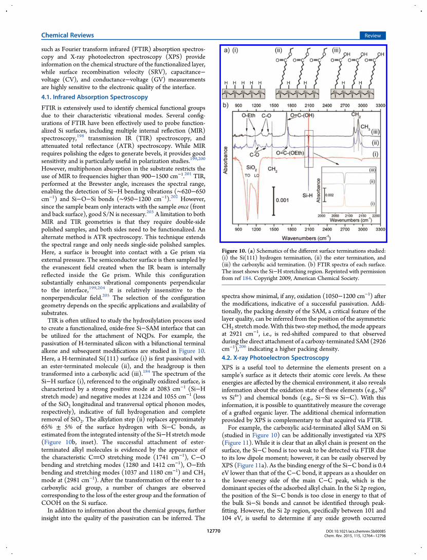
In the Langmuir technique, the solvent (often hexane, toluene,or chloroform) evaporates, leaving the NQDs spread across thesubphase surface (usually water). A mobile barrier is used toslowly compress the NQDs until a dense monolayer is formed, asmonitored via a Langmuir isotherm (surface pressure versusarea), as schematically shown in Figure 16a. The monolayer can
then be transferred to a variety of substrates using vertical(Blodgett) or horizontal (Schaffere) lift-off.281,283,287,288 Thetechnique is highly versatile and enables a great deal of controlover the resulting NQD monolayer. The size, shape, andcomposition of the NQDs can be varied.282,283,287,289−292 Inaddition, by controlling the compression process, the packingdensity and interparticle distance can be tuned.293 Collier et al.294
showed that a reduction in the interparticle distance caused byhigher compression induced the insulator-to-metal transition fora monolayer of silver nanocrystals.In evaporation-based self-assembly, the NQDs spontaneously
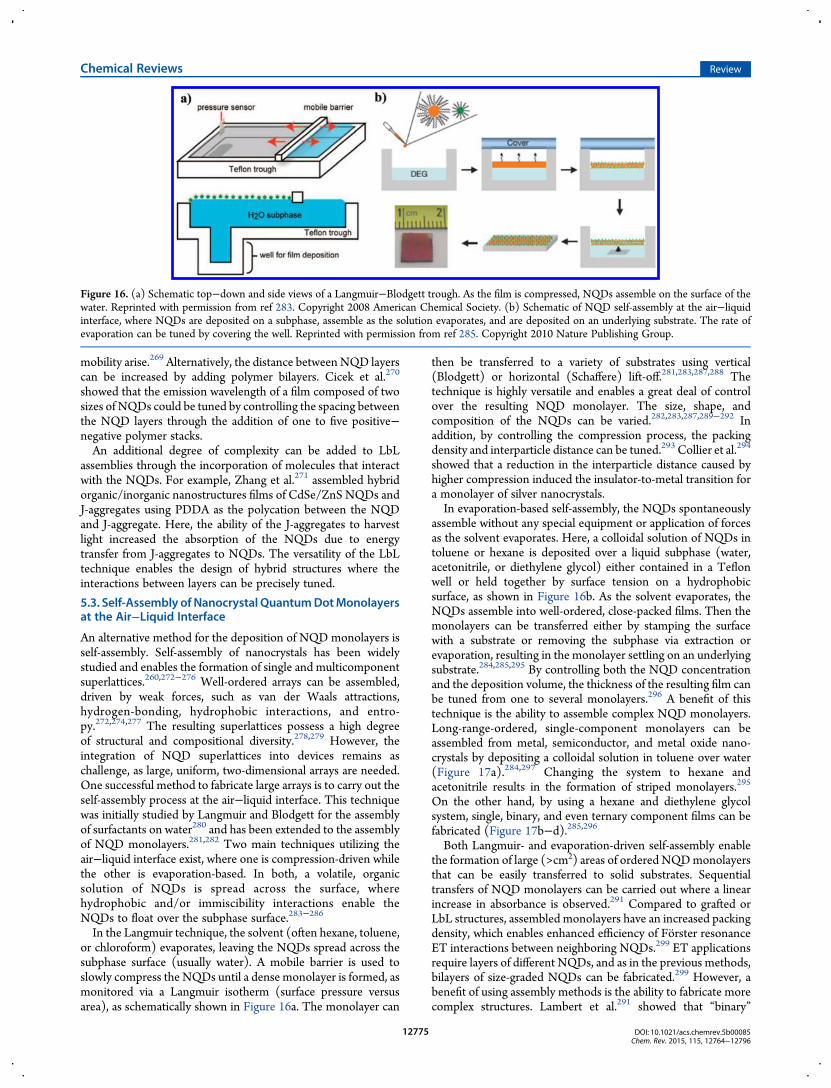
assemble without any special equipment or application of forcesas the solvent evaporates. Here, a colloidal solution of NQDs intoluene or hexane is deposited over a liquid subphase (water,acetonitrile, or diethylene glycol) either contained in a Teflonwell or held together by surface tension on a hydrophobicsurface, as shown in Figure 16b. As the solvent evaporates, theNQDs assemble into well-ordered, close-packed films. Then themonolayers can be transferred either by stamping the surfacewith a substrate or removing the subphase via extraction orevaporation, resulting in the monolayer settling on an underlyingsubstrate.284,285,295 By controlling both the NQD concentrationand the deposition volume, the thickness of the resulting film canbe tuned from one to several monolayers.296 A benefit of thistechnique is the ability to assemble complex NQD monolayers.Long-range-ordered, single-component monolayers can beassembled from metal, semiconductor, and metal oxide nano-crystals by depositing a colloidal solution in toluene over water(Figure 17a).284,297 Changing the system to hexane andacetonitrile results in the formation of striped monolayers.295
On the other hand, by using a hexane and diethylene glycolsystem, single, binary, and even ternary component films can befabricated (Figure 17b−d).285,296Both Langmuir- and evaporation-driven self-assembly enable
the formation of large (>cm2) areas of ordered NQDmonolayersthat can be easily transferred to solid substrates. Sequentialtransfers of NQD monolayers can be carried out where a linearincrease in absorbance is observed.291 Compared to grafted orLbL structures, assembled monolayers have an increased packingdensity, which enables enhanced efficiency of Forster resonanceET interactions between neighboring NQDs.299 ET applicationsrequire layers of different NQDs, and as in the previous methods,bilayers of size-graded NQDs can be fabricated.299 However, abenefit of using assembly methods is the ability to fabricate morecomplex structures. Lambert et al.291 showed that “binary”
Figure 16. (a) Schematic top−down and side views of a Langmuir−Blodgett trough. As the film is compressed, NQDs assemble on the surface of thewater. Reprinted with permission from ref 283. Copyright 2008 American Chemical Society. (b) Schematic of NQD self-assembly at the air−liquidinterface, where NQDs are deposited on a subphase, assemble as the solution evaporates, and are deposited on an underlying substrate. The rate ofevaporation can be tuned by covering the well. Reprinted with permission from ref 285. Copyright 2010 Nature Publishing Group.
Chemical Reviews Review
DOI: 10.1021/acs.chemrev.5b00085Chem. Rev. 2015, 115, 12764−12796
12775
structures could be fabricated by controlling the size of NQDs inthe different Langmuir layers. When the interparticle distanceratio of the larger to smaller NQDs is∼√3, a structure is formedwhere each large particle is surrounded by six smaller particles.With the correct composition of NQDs, this close-packedstructure could enhance ET between NQDs due to increasedinteractions with nearest neighbors. Cargnello et al.298 showedenhanced ET using self-assembled binary films of core−shellNQDs compared to simple mixtures.
6. ENERGY TRANSFER MECHANISMS FROMNANOCRYSTAL QUANTUM DOTS TO SILICON
6.1. Theoretical Considerations
Themain focus of this section is on themechanisms of ET into Sifrom neighboring photoexcited quantum emitters, such ascolloidal NQDs. We distinguish nonradiative ET (NRET) andradiative ET (RET)300 as qualitatively different contributions tothe overall ET enabled by near-field electromagnetic inter-actions.7,235,301,302 Dexter303 was probably the first to explicitlysuggest the idea of external NRET sensitization of inorganicsemiconductors for PV applications. The NRET mechanism isakin to the familiar Forster ET (with the usual acronym FRET)enabled by dipole−dipole interactions between neighboringmolecular species and depends on the spectral overlap of theenergy-donor emission and energy-acceptor absorption spec-tra.304−306 The NRET process corresponds to direct excita-tion307 of an electron−hole pair in a semiconductor by theelectric field of a decaying emitter’s exciton. While the NRETmechanism is frequently discussed in the literature for ET-hybrids,1,2,12,13,308−310 the potential significance of RET shouldnot be overlooked, as its relative contribution varies dependingon both the distance between the emitter and acceptor and thespectral range considered.7,302 In the RET process, the emitter’sexciton preferentially decays into photonic modes that can
propagate only within the energy-accepting semiconductor, thatis, waveguide modes in spatially confined semiconductor layersand wires.311 These modes are later absorbed and generateelectron−hole pairs, contributing to the electric current. Theeffective conversion of the incoming solar plane-wave photons,via re-emission from a relaxed localized exciton, into waveguidemodes may be compared to the effect from scattering processesachievable with metallic and dielectric structures judiciouslypatterned to increase the incident light absorption in thinsemiconductor layers.312,313
In order to accentuate the quantitative aspects of NRET andRET into layered planar Si structures and establish a theoreticalperspective, we follow here a model analysis presented in earlierpublications.7,301,302 The analysis considers how the decay rate ofan electric-dipole emitter is modified in proximity to a planarinterface, which can then be correlated with experimentalobservations of the emitter’s time-resolved PL (TRPL). Therehas been significant theoretical activity on this topic sinceSommerfeld’s original treatment of the problem of an antenna’semission near the earth’s surface.314 The problem is addressed inthe framework of macroscopic electrodynamics,311,315 whereelectromagnetic decay rates and emission patterns of oscillatingdipoles are calculated depending on the frequency (ω)-dependent complex dielectric functions ε(ω) = ε′(ω) + iε″(ω)of the media surrounding the dipole. This approach has beenapplied to emitters in different environments, leading to goodagreement with experimental data.311,315−317
In a vacuum, the lifetime τ0 (decay rate Γ0 = 1/τ0) of thespontaneous radiative decay of the emitter’s exciton311 isdetermined from the known
πεΓ =
| |ℏ
k p30
3 2
0 (5)
where k = ω/c = 2π/λ is the emission wavenumber and p is the(effective) dipole transition moment. The electromagnetic decayof the emitter changes in the vicinity of a planar interface, and themodified rate Γ can be expressed as
Γ Γ = + ∞I/ 1 (0, )0 (6)
For the randomly oriented transition dipole moment,averaging over its different orientations specifically yields eq 7:311
∫=−
− +
× −
I a b Reu u
uu r u r u
kz u
( , )d
2 1[(2 1) ( ) ( )]
exp(2i 1 )
a
b
22 (p) (s)
2(7)
Here, z is the distance from the emitter to the substrate, the effectof which is contained in the reflection coefficients r(s) and r(p) fors- and p-polarized waves as determined by the substrate’sdielectric properties. The integration variable u in eq 7 definesthe magnitude k∥ of the conserved in-plane components of thewave vector in terms of the vacuum wavenumber k: as k∥(u) = uk.The perpendicular components kz of the wave vector in a vacuumand silicon are, however, different and determined by
ε= − = −k u u k k u u k( ) (1 ) , ( ) ( )z z12 2 2
22 2 2
(8)
respectively. As applied to different regions in space, we note thatthe real values of the perpendicular components in eq 8 signifythe propagating waves while the imaginary values signify theevanescent ones. It is then instructive to divide eq 6 into parts forsome ranges of variable u that would correspond to differentdecay channels. Figure 18 shows the numerical results from the
Figure 17. (a) SEM image of a monolayer of CdSe/ZnS NQDs onsilicon assembled at the air−liquid interface using toluene and water. (b)SEM image of a ternary superlattice film self-assembled at the air−liquidinterface using hexane and diethylene glycol from two sizes of Fe3O4(16.5 and 7.0 nm) nanocrystals and 5.0 nm FePt nanocrystals. Thecolors indicate the three differently sized nanocrystals. Reprinted withpermission from ref 296. Copyright 2011 American Chemical Society.TEM images of binary superlattice films self-assembled at the air−liquidinterface using hexane and diethylene glycol from (c) CdSe/ZnS NQDsand Au/Fe3O4 nanocrystals and (d) PbSe/CdSe NQDs and Au/Fe3O4nanocrystals. Reprinted with permission from ref 298. Copyright 2014Wiley-VCH.
Chemical Reviews Review
DOI: 10.1021/acs.chemrev.5b00085Chem. Rev. 2015, 115, 12764−12796
12776
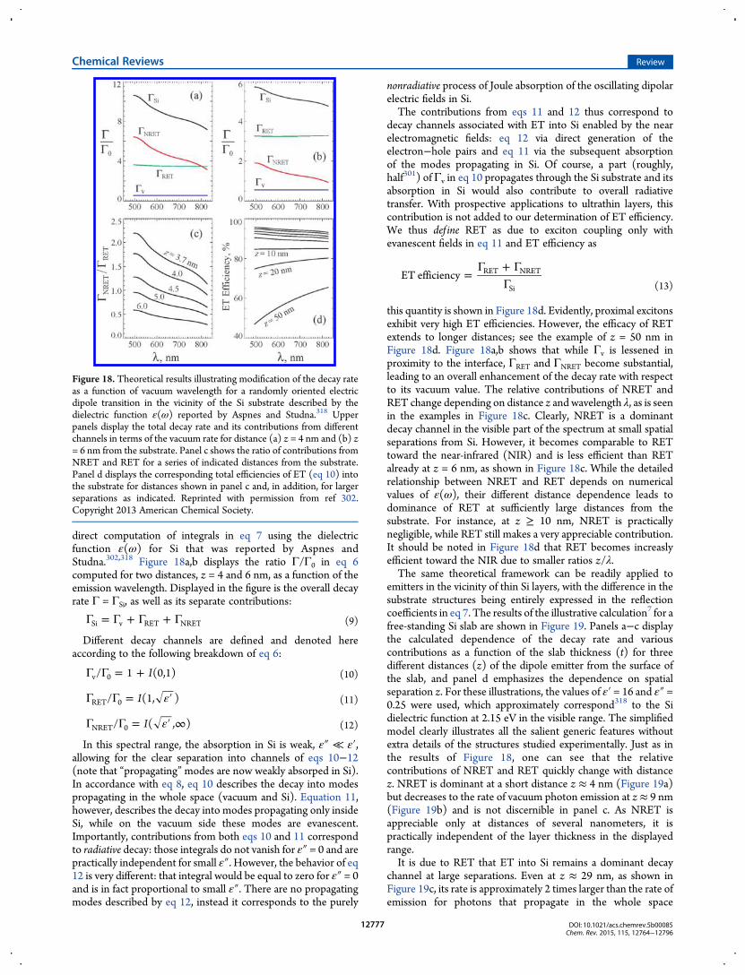
direct computation of integrals in eq 7 using the dielectricfunction ε(ω) for Si that was reported by Aspnes andStudna.302,318 Figure 18a,b displays the ratio Γ/Γ0 in eq 6computed for two distances, z = 4 and 6 nm, as a function of theemission wavelength. Displayed in the figure is the overall decayrate Γ = ΓSi, as well as its separate contributions:
Γ = Γ + Γ + ΓSi v RET NRET (9)
Different decay channels are defined and denoted hereaccording to the following breakdown of eq 6:
Γ Γ = + I/ 1 (0,1)v 0 (10)
εΓ Γ = ′I/ (1, )RET 0 (11)
εΓ Γ = ′ ∞I/ ( , )NRET 0 (12)
In this spectral range, the absorption in Si is weak, ε″ ≪ ε′,allowing for the clear separation into channels of eqs 10−12(note that “propagating”modes are now weakly absorped in Si).In accordance with eq 8, eq 10 describes the decay into modespropagating in the whole space (vacuum and Si). Equation 11,however, describes the decay into modes propagating only insideSi, while on the vacuum side these modes are evanescent.Importantly, contributions from both eqs 10 and 11 correspondto radiative decay: those integrals do not vanish for ε″ = 0 and arepractically independent for small ε″. However, the behavior of eq12 is very different: that integral would be equal to zero for ε″ = 0and is in fact proportional to small ε″. There are no propagatingmodes described by eq 12, instead it corresponds to the purely
nonradiative process of Joule absorption of the oscillating dipolarelectric fields in Si.The contributions from eqs 11 and 12 thus correspond to
decay channels associated with ET into Si enabled by the nearelectromagnetic fields: eq 12 via direct generation of theelectron−hole pairs and eq 11 via the subsequent absorptionof the modes propagating in Si. Of course, a part (roughly,half301) of Γv in eq 10 propagates through the Si substrate and itsabsorption in Si would also contribute to overall radiativetransfer. With prospective applications to ultrathin layers, thiscontribution is not added to our determination of ET efficiency.We thus def ine RET as due to exciton coupling only withevanescent fields in eq 11 and ET efficiency as
=Γ + Γ
ΓET efficiency RET NRET
Si (13)
this quantity is shown in Figure 18d. Evidently, proximal excitonsexhibit very high ET efficiencies. However, the efficacy of RETextends to longer distances; see the example of z = 50 nm inFigure 18d. Figure 18a,b shows that while Γv is lessened inproximity to the interface, ΓRET and ΓNRET become substantial,leading to an overall enhancement of the decay rate with respectto its vacuum value. The relative contributions of NRET andRET change depending on distance z and wavelength λ, as is seenin the examples in Figure 18c. Clearly, NRET is a dominantdecay channel in the visible part of the spectrum at small spatialseparations from Si. However, it becomes comparable to RETtoward the near-infrared (NIR) and is less efficient than RETalready at z = 6 nm, as shown in Figure 18c. While the detailedrelationship between NRET and RET depends on numericalvalues of ε(ω), their different distance dependence leads todominance of RET at sufficiently large distances from thesubstrate. For instance, at z ≥ 10 nm, NRET is practicallynegligible, while RET still makes a very appreciable contribution.It should be noted in Figure 18d that RET becomes increaslyefficient toward the NIR due to smaller ratios z/λ.The same theoretical framework can be readily applied to
emitters in the vicinity of thin Si layers, with the difference in thesubstrate structures being entirely expressed in the reflectioncoefficients in eq 7. The results of the illustrative calculation7 for afree-standing Si slab are shown in Figure 19. Panels a−c displaythe calculated dependence of the decay rate and variouscontributions as a function of the slab thickness (t) for threedifferent distances (z) of the dipole emitter from the surface ofthe slab, and panel d emphasizes the dependence on spatialseparation z. For these illustrations, the values of ε′ = 16 and ε″ =0.25 were used, which approximately correspond318 to the Sidielectric function at 2.15 eV in the visible range. The simplifiedmodel clearly illustrates all the salient generic features withoutextra details of the structures studied experimentally. Just as inthe results of Figure 18, one can see that the relativecontributions of NRET and RET quickly change with distancez. NRET is dominant at a short distance z ≈ 4 nm (Figure 19a)but decreases to the rate of vacuum photon emission at z≈ 9 nm(Figure 19b) and is not discernible in panel c. As NRET isappreciable only at distances of several nanometers, it ispractically independent of the layer thickness in the displayedrange.It is due to RET that ET into Si remains a dominant decay
channel at large separations. Even at z ≈ 29 nm, as shown inFigure 19c, its rate is approximately 2 times larger than the rate ofemission for photons that propagate in the whole space
Figure 18. Theoretical results illustrating modification of the decay rateas a function of vacuum wavelength for a randomly oriented electricdipole transition in the vicinity of the Si substrate described by thedielectric function ε(ω) reported by Aspnes and Studna.318 Upperpanels display the total decay rate and its contributions from differentchannels in terms of the vacuum rate for distance (a) z = 4 nm and (b) z= 6 nm from the substrate. Panel c shows the ratio of contributions fromNRET and RET for a series of indicated distances from the substrate.Panel d displays the corresponding total efficiencies of ET (eq 10) intothe substrate for distances shown in panel c and, in addition, for largerseparations as indicated. Reprinted with permission from ref 302.Copyright 2013 American Chemical Society.
Chemical Reviews Review
DOI: 10.1021/acs.chemrev.5b00085Chem. Rev. 2015, 115, 12764−12796
12777

(“vacuum photons”). Figure 19d displays the data for a broaderrange of distances. A closer inspection of the data shows that therates of decay due to RET and vacuum photons are comparableat roughly distances z ∼ 0.1λ0. In the model example, thiscorresponds to approximately 50% efficiency of ET into Si from
distances z as long as 50 nm. Figure 19a−c also illustrates theoscillations of RET as a function of slab thickness t, and theseoscillations are related to the strength of the dipole emissioncoupling to waveguiding modes in the slab. The oscillationsoccur with respect to the value that would take place for a dipolenear the bulk Si substrate presented in Figure 18. Only forextremely thin layers does RET become noticeably smaller.Remarkably, these model results thus show that ET can be asefficient into ultrathin Si nanomebranes (perhaps as thin as∼100−200 nm) as it is into bulk Si substrates. When combinedwith the efficacy of ET over a broad spectral range shown inFigure 18, these observations suggest that ET-sensitization ofultrathin Si layers may be utilized in PV devices.
6.2. Determination of NRET Efficiencies from NanocrystalQuantum Dots to Semiconductor Substrates
The field of ET between molecular absorbers or semiconductorNQDs and various semiconductor surfaces for the purpose ofphotovoltaic light harvesting has seen something of resurgence inthe past few years. Particularly, GaAs and silicon surfaces havebeen employed in order to improve efficiencies of the existingtechnologically important solar cells, where GaAs-basedstructures pertain to very high-efficiency (and possibly multi-junction) cells while Si structures are thought to become moreefficient for thin film geometries. Clear illustrations of theviability of the energy-transfer-based concepts first started toemerge in experimental studies of NQDs on GaAs substrates, inwhich the NRET efficiency was predicted to be substantialthanks to the large absorption coefficient of GaAs arising from itsdirect band gap transitions.The efficiencies of ET can be measured via temporally and
spectrally resolved PL spectroscopy. This technique is a valuabletool that can be used to monitor the presence and dynamicalbehavior of correlated electrons and holes in semiconductormedia and is extensively described in a number of books.319,320 Ina typical PL system, the sample is excited by a laser [either incontinuous (cw) or pulsed mode] promoting electron−holepairs into higher energy states above the band gap of thesemiconductor (Figure 20a). The excitations then undergoenergy and momentum relaxation toward the band gapminimum, undergoing Coulomb scattering and interactionwith phonons. Finally, the electrons recombine with holes,resulting in the emission of photons. The spectral position andtime evolution of the emission (derived from TRPL measure-ments) provide valuable information about the nature of theelectronic states in a semiconductor. Additionally, a number of
Figure 19. Model decay rates, in units of Γ0, of a randomly orientedpointlike electric dipole emitter at distance z from a free-standing Silayer. The dielectric function of Si used here for calculations is ε = 16 +0.25i. Panels a−c display decay rates as a function of the layer thickness tand differ by the distance-to-the-layer, as measured in vacuumwavelengths λ: (a) z = 0.007λ, (b) z = 0.015λ, and (c) z = 0.05λ. Thelayer thickness is measured by the wavelengths in Si, λSi = λ/4. The solidblack lines depict the total decay rate as expressed by eq 9. Thecontributions to this total rate are displayed as follows: green lines forΓRET from the excitation of waveguiding modes in Si (eq 11), blue linesfor Γv from the excitation of vacuum photons (eq 10), and red lines forΓNRET from NRET into Si (eq 12). The benchmark results for the totaldecay rate in the vicinity of the bulk Si substrate are shown as blackdashed-line levels. Panel d displays the dependence on distance z forseveral values of the layer thickness as indicated. NRET is the majorcontributor to Γ at distances smaller than∼0.01λ, while RET dominatesat larger separations up to ∼0.1λ. Reprinted with permission from ref 7.Copyright 2012 American Chemical Society.
Figure 20. (a) Schematic of the microscope-based PL system used to study ET from NQD to silicon surfaces. Manifestations of the ET process: (b)reduction of the PL intensity of the donor and simultaneous enhancement of the PL intensity of the acceptor and (c) shortening of the PL lifetime of thedonor in the presence of the acceptor. Reprinted with permission from ref 301. Copyright 2013 Optical Society of America.
Chemical Reviews Review
DOI: 10.1021/acs.chemrev.5b00085Chem. Rev. 2015, 115, 12764−12796
12778

extrinsic processes, often related to the presence of so-called“trap” states that are able to scavenge charge carriers, caninfluence the PL properties, thus making this technique avaluable tool for defect characterization.During the ET process, the emission of the donor molecule or
NQD is quenched while the emission of the acceptor molecule isenhanced (Figure 20b). The degree of the quenching/enhance-ment provides a quantitative measure of the ET efficiency.However, this ratiometric appoach is not always reliable, as itrequires precise knowledge of the sample’s optical density andemissive properties and matching the sample’s exact excitation/collection conditions with those of a reference. A more preciseapproach is to monitor changes in the PL dynamics of a donor inthe presence of an acceptor (Figure 20c). The PL lifetime of thedonor is independent of the excitation/collection conditions andonly reflects modifications to the exciton relaxation pathways dueto the introduction of additional decay channels, such as ET. Thisargument is especially true for donors deposited on semi-conductor acceptor substrates. Here, the excitation/collectionconditions of the donor NQDs are dramatically different whencompared to donor NQDs deposited on noninteractingsubstrates (usually glass or quartz). This change arises as adipole’s emission pattern and excitation conditions are verydifferent when placed in the vicinity of a highly polarizabledielectric substrate (GaAs or Si), thus leaving the measurementof changes in the donor PL lifetime as a true measure of ETinteractions.301
NRET from near-infrared active PbS NQDs emitting at ∼965nm to buried InGaAs quantum wells was shown by Lu et al.308
Quantum wells made from short-period superlattices wereburied approximately 3 nm below the sulfur-passivated GaAssurface. A drop-cast layer of NQDs was deposited on the top ofthe structure, with approximately 8 nm separating the monolayerand quantum wells. To eliminate charge carrier feeding byelectron−hole pairs generated in the substrate, the excitationwavelength was set to 910 nm. The authors observed about a35% reduction in the NQD PL intensity as compared to thereference substrate without buried quantum wells. Additionally,the average PL decay time decreased from 298 ns on GaAs to 208ns on the buried well structure, as seen in Figure 21. On the basisof these measurements, the authors estimated a nonradiativetransfer decay time of∼690 ns compared with the radiative decaytime of 960 ns for the PbS NQDs. That corresponds to ∼30%
nonradiative transfer efficiency to the quantum wells from theseNQDs. Another important achievement was the demonstrationof a NRET-induced photocurrent in GaAs patterned quantumwells sensitized with CdSe/ZnS NQDs.310 By comparison of thePL decay times, the authors estimated the efficiency of NRETfrom NQDs to the proximal semiconductor surface to be 79%.Additionally, photocurrent measurements revealed a 6-foldenhancement for the patterned hybrid devices when comparedto the reference p−i−n structure. From the data, the authorsconcluded that approximately 89% of the exciton energy wastransferred into the quantum wells via NRET from the proximalNQDs. They also noted that such hybrid configurations are notlimited to using NQDs as energy donors but should also beapplicable to other strongly absorbing, solution-based materials.The studies discussed above were based on NQDs that were
drop-cast onto semiconductor surfaces. In such situations,unprepared interfaces may have a substantial number of surfacetrapping sites that will facilitate exciton dissociation andsubsequent charge trapping. This is especially important whenTRPL dynamics are recorded as the method of choice to registerNRET signaturesfaster dynamics of the emitting donor (NQDor molecule) species indicate an energy transfer channel.However, other nonradiative channels present such as interfacecharge trapping would similarly affect dynamics, thus hinderingNRET effects. Further, drop-casting does not allow for uniformlayer deposition, thus providing for a multitude of donor−acceptor distances, complicating interpretation of the PLlifetimes. Recently, several publications have achieved control-lable positioning of monolayers of NQDs on Si surfaces, thusallowing for a quantitative determination of the energy transferrates. Nguyen et al.235 discussed NRET from a monolayer ofCdSe/ZnS NQDs controllably grafted on a SAM-passivated Sisurface, as described in section 5.1. TRPL measurementsrevealed a progressive shortening of the PL lifetime of thedonor NQDs as the separation from the acceptor Si surfacedecreased with ∼1/d3 dependence, confirming its dipole−dipoleorigin. The calculated NRET efficiency at 565 nm reached 65%with an interaction distance of about 4.4 nm. Extension of NRETto the near-infrared wavelength range was accomplished byNimmo et al.,302 who similarly grafted a monolayer of CdSe/ZnSor CdSeTe/ZnS NQDs emitting between 545 and 800 nm on aSi surface. There, the efficiency of NRET was found to decreasefrom ∼70% to <50%, mostly owning to the lower absorption ofSi at longer wavelengths, as seen in Figure 22. We would like tonote that precise measurements of NRET rates were possible dueto the fact that NQDs were grafted within a monolayer on thesubstrate, thus avoiding complications in the PL lifetimesignatures that arise from a distribution of distances andassociated NRET rates. Later on, another study of NRET wasperformed by Andreakou et al.,13 who drop-casted PbS NQDsemitting at∼900 nm and obtained a transfer efficiency estimatedat 44%.
6.3. Energy Transfer in Nanocrystal Quantum Dot Solids onSilicon
An important element pertaining to the efficiency of solarharvesting is the energy transfer mechanism within thenanocrystal solid itself. Dense, multilayer, light-absorbing,excitonic materials are required for efficient sunlight collection.Once such multilayer films were assembled on the Si substrates(either via drop-casting, grafting, or assembly), several ETpathways were found to be operational. The major one comesfrom interdot NRET that leads to energy outflow from species
Figure 21. (a) Time-resolved PL of PbS NQDs on passviated GaAs(blue) and on passivated near surface quantum wells (red), excited at900 nm (below GaAs band gap) and detected at 965 nm (PbS PL peak).The decay of the TRPL curves is fitted using a stretched exponentialfunction. (b) Schematic showing an architecture comprising NQDabsorbers embedded in a vertical array of high-mobility channels thatallow nonradiative transfer of excitons from the adjacent NQDs andsimultaneously provide high-mobility transport. Reprinted withpermission from ref 308. Copyright 2007 American Chemical Society.
Chemical Reviews Review
DOI: 10.1021/acs.chemrev.5b00085Chem. Rev. 2015, 115, 12764−12796
12779
with larger band gaps (such as smaller size NQDs) to ones withsmaller band gaps (larger NQDs) within the ensemble. Earlyexperiments with NQD bi- and multilayers assembled on glasssurfaces (in the absence of Si) have shown this process to beefficient if there is good spectral overlap between donor andacceptor species (i.e., proper size difference in the case ofcolloidal NQDs).222,266,267,269,299 In size-gradient NQD films,NRET times as fast as 100 ps and recapture of the excitonstrapped at surface states have been demonstrated. One of the firstdemonstrations of size-gradient NQD solids assembled on aninteracting substrate was shown by Kramer et al.321 Theyassembled a graded multilayer film of PbS NQDs on TiO2substrates. The graded structure drives minority electrons alongthe built-in electric field formed by the semiconductorheterojunction at the TiO2/PbS NQD interface. Due to theparticular band gap alignment of quantum-confined PbS NQDs,conduction band offsets form a so-called “quantum funnel”,driving electrons from smaller NQDs to larger ones and towardthe collecting TiO2 substrate, while valence band offsets remainconstant and do not subject holes to an additional driving force.When compared to a control, ungraded device (where all NQDsare the same size) with the same amount of absorption in theNQD layer, marked improvements in the fill factor, open circuitcurrent, and short circuit voltage are achieved for the gradeddevices. Additionally, the relative conversion efficiency increasedby 35% (from 2 to 2.7% overall efficiency). The authors ascribedthe observed effect entirely to electron funneling, although it islikely that cascaded NRET between size-gradient NQD layers isalso a contributing factor.Later, size-gradient bilayer films on Si were demonstrated by
Yeltik et al.268 In this work, two disparate sizes of NQDs emittingat ∼550 nm (“green” NQDs) and at ∼635 nm (“red” NQDs)were assembled on Si via LbL assembly with PDDA−PSS used asa separation layer between the NQD adsorption layers, as shownin Figure 23. This work demonstrated ET efficiency from the toplayer (GQD) to the bottom layer (RQD) at ∼40% withsubsequent 80% transfer from the RQD to Si, resulting in a 32%overall transfer probability for an exciton in the GQD layer to gointo the Si substrate. Recently, DeBenedetti et al.,220 were able toconsecutively graft monolayers of “green” (emission at 545 nm)and “red” (585 nm) NQDs on a prefunctionalized Si surfaceusing amine-modified linkers. Such a configuration provides
shorter distances between two interacting NQD layers,increasing the NRET efficiency between layers above 90%.The transfer efficiency from the bottom-most layer (red NQDs)into the Si substrate was also maintained at ∼90% in accordancewith previous research7,302 and the total transfer efficiency fromthe green NQD layer to the Si substrate was hence estimated tobe ∼85%. A comparison to reference bilayers grafted on glasssubstrates and theoretical modeling revealed that the observedtransfer efficiency from the outmost layer to Si is close to thetheoretical limit of 90%. Hence, the size-gradient structuresformed via grafting on functionalized Si substrates allow for thegrowth of defect-free nanocrystal solids that will be suitable forphotovoltaic and photodetector/sensor applications and couldbe incorporated into mature Si technologies. Additionally, Yeltiket al.309 studied the temperature dependence of energy transferfrom multilayers formed by spin-casting concentrated NQDsolutions (∼10 monolayers as determined by ellipsometry, SEM,and AFM) on oxidized Si substrates. The separation between theNQD solid and Si was varied by introducing Al2O3 spacers ofdifferent thicknesses. The PL lifetime measurements of suchNQD solids at different temperatures (20−300 K) revealed thatNRET becomes weaker at lower temperatures. This behaviorwas attributed to a reduction of phonon interband transitions inSi, which lowers Si absorption at lower temperatures.6.4. Radiative Energy Transfer to Silicon Substrates
In addition to the purely electrostatic dipole−dipole interactionthat constitutes the NRET process, RET was experimentallydemonstrated to be operative and very efficient across a widewavelength range. This process involves the coupling of thedonors’ emission into the waveguide modes of the high-refractive-index semiconductor substrate. Following the the-oretical description provided in section 6.1, Nguyen et al.7 used amonolayer of CdSe/ZnS NQDs grafted on thin Si nano-membranes (SiNM) of different thicknesses (t = 25−300 nm)and varied the distance (d) to Si as, shown in Figure 24c. The PLlifetimes were observed to exhibit oscillating behavior as afunction of the SiNM thickness as a result of the PL coupling tovarious waveguide modes (Figure 24a,b). The maximum RETcoupling efficiency was observed for a SiNM thickness of 75 nm,which corresponds to the half-wavelength of the donor emission(vacuum emission wavelength λ0 = 565 nm) within the Simaterial. Overall, the ET efficiency to the SiNM was found to bearound 90%, for the minimum NQD-to-Si separation (d = 4.4nm), whereas the NRET efficiency was 58% and the RET 29%.The relative effects of these contributions were reversed at largerseparation distances, due to the larger effective length of the RET
Figure 22. (a) PL emission spectra of different NQDs emitting from 545to 800 nm as grafted on SiO2. NQDs on Si exhibit the same PL profile.(b) Schematics of energy transfer from NQDs emitting at differentwavelength to Si substrate. (c) Total ET efficiency (Etotal) shown byblack squares along with separate contributions ENRET from NRET (redcircles) and ERET from RET (blue triangles). Reprinted with permissionfrom ref 302. Copyright 2013 American Chemical Society.
Figure 23. (a) Schematic for the gradient energy transfer from thecascaded GQD/RQD bilayer into bulk Si. (b) Emission and absorptionspectra of CdTe GQDs and CdTe RQDs (green and red curves,respectively), and absorption spectrum of bulk Si (blue curve).Reprinted with permission from ref 268. Copyright 2013, AIPPublishing LLC.
Chemical Reviews Review
DOI: 10.1021/acs.chemrev.5b00085Chem. Rev. 2015, 115, 12764−12796
12780

interaction (d ∼ 0.1λ0). At d = 12.6 nm, the RET and NRETefficiencies were 52% and 21%, respectively, while at d = 18.6 nm,the RET efficiency was 57.5% and the NRET efficiency was only5.5%. These results clearly indicate that (1) RET coupling is amajor, long-distance mechanism contributing to the overall ETand (2) the total ET into very thin SiNMs can be as effective asinto bulk Si, but not at the expense of NRET. Further detailedevidence of the emission coupling into the Si substrate waspresented by Nguyen et al.,301 who studied the PL emission fromCdSe/ZnSNQDmonolayers on Si for separation distances of upto 500 nm. The authors observed a clear oscillatory behavior ofthe PL lifetimes as a function of the separation distance due tofield interference effects. Strong directionality of the PL emissionand its preferential coupling into the Si substrate was alsodemonstrated, confirming the effectiveness of the waveguidecoupling mechanism.
6.5. Nanocrystal Quantum Dot Sensitization ofNanostructured Silicon Substrates
There have been a number of experiments aimed at sensitizing SiNWs and NPs with colloidal nanocrystals or molecules. The goalwas to take advantage of the improved light collection afforded insuch structures due to the increased surface area available fordonor molecule placement and enhanced light collectionproperties of the Si nanostructures themselves. By drop-castinga layer of CdSe NQDs on Si radial p−i−n junction NPs,
Guzelturk et al.322 demonstrated that NQDs can be utilized asefficient wavelength up-converters to harvest incident photonsthat are otherwise poorly absorbed in Si at short wavelengths andconvert them into longer wavelengths photons that can be betterabsorbed by Si. A relative enhancement of solar cell efficiency of∼13% over a nonsensitized cell was observed, albeit the absolutelight-harvesting efficiency remained low (∼2%). Similarly, Songet al.323 examined a thin layer of drop-casted PbS NQDsdeposited on arrays of n-doped Si NWs. After optimization of themorphology and deposition parameters, an external photo-conversion efficiency (PCE) of 6.5% was achieved. However, nospecific attempts were made to passivate the Si surface orassemble the NQD solid in a controllable manner. As a result,these studies could not demonstrate an ET-related efficiencyenhancement. Later, Seitz et al.324 utilized a monolayer of CdSe/ZnS NQDs grafted on upright standing Si NPs (pillar height ∼4um, diameter 300 nm, center to center separation ∼500 nm). PLintensity measurements revealed that the number of NQDs perunit area increased proportionally to the surface area of the SiNPs. These measurements, along with SEM images confirmingNQD grafting on the sides of the NPs (as seen in Figure 25),support the idea that Si NPs can be used as scaffolds for futuredevelopment of dense NQD solids.Lu et al.12 also drop-casted PbS NQDs on a planar array of Si
NWs and observed, for the first time, an ET-induced photo-
Figure 24. (a) Relative acceleration of the NQD exciton decay with respect to the reference glass sample as a function of the thickness, t, of the SiNM.The data points and theoretical curves are grouped by different values of the silicon oxide spacer thickness (d). The distance of the dipole emitter fromthe top surface is taken as z = 4 nm for the red theoretical curve and z = 3.7 nm for the green and blue ones. The dielectric parameters of Si used forcalculations are ε′ = 16.5 and ε″ = 0.32. Here the data points are shown with the reference τG = 22.8 ns. (b) Efficiency of ET into Si as extracted from thecolor-coordinated theoretical curves in panel a. The solid lines correspond to the total ET efficiency [(ΓRET + ΓNRET)/Γ], and the dashed lines show therelative efficiency of ET just via waveguide modes in the SiNM (ΓRET/Γ). (c) Schematics of different NQD/SiNM structures used to extract the relativeparticipation of various decay channels: schematically displayed are NRET and RET processes from NQDs into the underlying Si slab as well as intoSiO2 substrate (on the rightmost structure). The role of NRET is strongly diminished with a thicker spacer (the leftmost structure), while the waveguidemodes in Si are efficiently excited. (Top right) AFM images of NQDs attached via carboxy-terminated alkyl chains on an oxide-free SiNM surface. The 5× 5 μm image emphasizes the homogeneity of the NQDs’ monolayer attachment, while the 1 × 1 μm confirms the individuality of the NQDs tominimize interdot ET effects. Reprinted with permission from ref 7. Copyright 2012 American Chemical Society.
Chemical Reviews Review
DOI: 10.1021/acs.chemrev.5b00085Chem. Rev. 2015, 115, 12764−12796
12781
current in the Si substrate. TheNRET efficiency was estimated tobe approximately 15−40%. Amore complete description of theseresults is provided in section 7. However, the Si NW’s surface wasnot specifically functionalized in this case and the drop-cast NQDlayer was sufficiently thick and noncoordinated (as evidenced bystrong interdot energy transfer within the NQD ensemble), sothat only the NQDs sufficiently close to the Si surfacecontributed to the photocurrent, explaining the fairly low ETefficiency. From these results, it is clear that a fundamentalunderstanding of surface and interface defects in complexgeometries, such as nanopillars and nanowires, is important toreduce surface and interface recombination. Further efforts toassemble size-gradient, dense NQD films on Si nanostructuredsubstrates are expected to improve conversion efficiency.6.6. Multiexciton Generation and Singlet Exciton Fission inApplications to Silicon Sensitization
Emerging concepts in advanced solar energy conversion (third-generation photovoltaics) have been widely discussed.9 Amongthem are hot carriers, up-and-down conversion, solar concen-trators, multiexciton generation (MEG), and singlet fission (SF)solar cells. The last two attract particular interest, since they canpotentially be used to overcome the Shockley−Quisser (SQ)single junction limit. It has been shown, theoretically and laterexperimentally, that the MEG process is more efficient instrongly confined NQDs as compared to bulk semiconductorsdue to enhanced carrier−carrier Coulomb interactions innanoscale volumes. An extensive description of these activitiesexists in several reviews and references therein.325,326 While therehave been some reports of improved solar cell performance dueto MEG effects327 and new types of NQDs with enhanced MEGproperties have been developed,328 there has not been a reporton MEG-active NQDs coupled to Si substrates.A sort of analog of MEG in NQDs is the process of SF in
organic semiconductors. In SF, one higher energy singlet excitonundergoes spontaneous fission into two lower energy tripletexcitons, each with ≤1/2 (singlet energy) ± ∼kT. SF wasobserved for a variety of polyacene crystals. In an ideal situation,SF doubles the photogenerated current at a given band gap329
and has therefore been suggested as a route to increasemultijunction PV efficiencies. It is interesting to note that inhis original paper303 on excitonic sensitization of inorganicsemiconductors, Dexter discussed such triplet excitons charac-terized by very long diffusion lengths. Some experimentalprogress in the utilization of triplet excitons for PVs wasdemonstrated recently, but in charge-transfer-based hybrids.Ehrler et al.330 created a solar cell that collects photocurrent fromtriplet excitons created by singlet fission in pentacene and low-energy photons absorbed in PbS NQDs without requiringtandem geometry. It was found that triplet excitons can
dissociate at the organic−inorganic interface, as seen in Figure26. Preliminary device optimization yielded solar cells with PCEs
approaching 1% under 1 sun illumination and internal quantumefficiencies greater than 50%. Further work331 by the same groupresulted in a demonstration of a pentacene/PbSe/α-siliconesolar cell with its performance enhanced by SF in pentacene withsubsequent triplet separation at the PbSe/organic interface andcollection into the Si substrate. However, the efficiency of thetriplet formation and subsequent transfer was not specificallyreported, although the overall solar cell performance was ∼2%.Whether triplet excitons resulting from SF can be utilized in
ET-based hybrid PV structures remains to be seen. Under-standably, some spin-flipping mechanisms should be involved,which could lead to the decrease of ET efficiency. In an attemptto experimentally address Dexter’s original proposal, Piland etal.332 studied molecular excitation dynamics in tetracenedeposited on Si surfaces with a LiF layer used as an inert spacerbetween the materials. In this work, the authors studied theemission from singlet exciton states in tetracene created by thepump laser (prompt fluorescence) and emission from singletstates created by triplet−triplet fusion (delayed fluorescence).The delayed fluorescence is a long-lived process (ca. hundreds ofnanoseconds) where its time scale is defined by the characteristictriplet diffusion and recombination (fusion) times. While it wasobserved that the PL intensity and fluorescence lifetime of theprompt fluorescence varied as a function of distance from thesubstrate, in accordance with theory, the measured PL lifetime ofthe delayed fluorescence was not found to depend on thedistance to Si. These observations were interpreted as evidencefor the absence of triplet quenching by Si.Utilization of triplet excitons can also be envisioned in a
scenario where they are first converted into singlet states beforeET into a semiconducting substrate occurs. A new possibility ofan efficient route for such a conversion was demonstratedrecently by Thompson et al.,333 who observed direct excitonicenergy transfer from “dark” triplets in tetracene to colloidal PbSNQDs, enabling control of molecular triplet excitons in the NIR.Steady-state excitation spectra combined with transient photo-luminescence studies showed that the transfer efficiency could behigher than 90%. The transfer efficiency was found to dependexponentially on the ligand length separating the donor tetracene
Figure 25. (a−c) Cross-sectional SEM images of Si NP NQD hybridstructures. Well-resolved individual NQDs are observed in themagnified view (c). Reprinted with permission from ref 324. Copyright2012, AIP Publishing LLC.
Figure 26. Device schematic, energy diagram, and proposed workingmechanism of pentacene/PbS solar cells. The excited singlet state in thepentacene layer converts to two triplet states after about 80 fs. Thesetriplets are dissociated at the pentacene/PbS nanocrystal interface. Atthe same time, the PbS nanocrystal absorbs the infrared part of theincident light. Reprinted with permission from ref 330. Copyright 2012American Chemical Society.
Chemical Reviews Review
DOI: 10.1021/acs.chemrev.5b00085Chem. Rev. 2015, 115, 12764−12796
12782

molecule from the acceptor PbS NQD. On the basis of theirobservations, the authors concluded that the transfer mechanismincludes the Dexter hopping process consisting of ET mediatedby the concurrent exchange of two electrons. It was thenproposed that semiconductor nanocrystals, known to be able toefficiently transfer energy to bulk silicon via the Forstermechanism, be employed as a “relay” to transfer excitonic energyfrom organic molecules into conventional solar cells. This couldenhance the PCE as SF can create two triplets for each absorbedphoton and potentially double the photocurrent. These resultshighlight the opportunities presented by hybrid organic−inorganic structures and suggest that transferring excitonsbetween the two components may require more complexorganizations and chemical approaches.
7. ELECTRICAL MEASUREMENTS OFQUANTUM-DOT-MODIFIED SILICONNANOSTRUCTURES
Nowadays, most NQD-based solar cells rely on charge transfereither within the colloidal quantum dot film, such as Schottkycells,334 depleted heterojunction colloidal quantum dot solarcells,335 and quantum funnel cells,321 or across the NQD/semiconductor interface in a type of structure similar to dye-sensitized solar cells.336 However, for these solution-depositedNQD films, the carrier mobility is commonly a limiting factor.Even with optimal ligand exchange,337,338 achieved by replacingthe insulating organic ligands with inorganic molecularcomplexes and thus reducing the interdot spacing from ∼2 nmto <0.5 nm, the electron mobility is still less than 30 cm2 V−1 s−1
and the hole mobility is below 1 cm2 V−1 s−1. At the present time,the PCE of NQD-based solar cells is around 6−8%.339,340The concept of excitonic energy transfer has been applied to
the development of NQD-based optoelectronic devices, withobvious advantages compared to direct charge transfer. Inaddition to the increased interaction range (10−100 nm)compared to sub-nanometer coupling distances inherent to thecharge-transfer process, the energy transfer process to Si has beenshown to be quite efficient at the elementary level,7 withefficiency exceeding 90% for a single layer of NQDs grafted on Siby combining both NRET and RET channels. The chemicalgrafting process has been shown to work for NQDs across abroad range of emission wavelengths302 and can be extended to3D assembly for directional energy funneling.220,309,341 However,most of the experimental evidence comes from spectroscopicmeasurements,7,220,235,268,302,309,342 especially TRPL. In contrast,only a few electrical measurements have been performed toinvestigate the energy transfer process.12,310,322,343
7.1. Direct Photocurrent Measurements
For photovoltaic devices, the incorporation of NQDs is expectedto improve the overall PCE or enhance the device photocurrentdue to energy transfer from NQDs. Initially, such measurementshave been performed for GaAs p−i−n multiple quantumwells,310 bulk GaAs p−i−n heterostructures,343 and radial p−i−n junction Si NP arrays.322 Since the NRET process dependson the separation distance, it is important to minimize thedistance between theNQDs and the intrinsic region, for instance,by using patterning (nanotrenches or nanopillars) as shown inFigure 27a. A larger enhancement in device performance wasobserved for patterned devices with incorporated NQDs ascompared to reference flat devices. As seen in Figure 27d, for thecase of GaAs multiple quantum wells,310 the photocurrent of thepatterned device was found to be 6 times larger than that of the
flat device due to ET from NQDs in the sidewalls of the intrinsicGaAs quantumwell. Strong evidence for ETwas also provided byexamination of the TRPL decay for both the NQDs (Figure 27c)and the quantum well itself (Figure 27b). An energy influx fromNQDs to the quantum well results in the delayed rise time of theacceptor (QW) emission, as indicated by the arrow in Figure 27b,and the shortening of the NQD lifetime, both being clearsignatures of the NRET process. Improving their design byutilizing a bulk GaAs p−i−n heterostructure,343 the authorsshowed improved carrier transport that resulted in a 2 order ofmagnitude increase in photocurrent. However, in both reports,there was no mention of either the photocurrent wavelengthdependence or the PCE under common solar cell testingconditions.Guzelturk et al.322 combined CdSe NQDs with radial p−i−n
junction Si NP arrays and observed a 13% enhancement inoverall solar cell conversion efficiency under AM1.5G conditions.Although the device’s open circuit voltage (Voc) barely changed,the increase in PCE mainly originated from the increase (up to 6times) in the external quantum efficiency (EQE) in the UVregion after the incorporation of NQDs, thus increasing thedevice short circuit current (Isc). This wavelength up-conversioneffect was explained by the strong absorption of NQDs in the UVregion and re-emission of photons that were trapped and finallyabsorbed by the NP structure, similar to the RET processmentioned earlier. Although the device EQE as a function of theexcitation wavelength was recorded, no peak structure near theNQD absorption peak at 568 nm was observed.However, a common shortcoming of these studies is the poor
performance of the starting device (even without patterning).The PCE was below 2% for the flat GaAs bulk heterostructuredevice at 570 nm and around 3% for the flat planar Si solar cellunder AM1.5G conditions. The patterning step (ion milling, wetetching, etc.) induces damages to the sidewalls of the trenchesand NPs, leading to worse performance for the patterned devices(a PCE reduction of more than 5 times for bulk GaAs p−i−nheterostructures and∼50% for the Si NP arrays in comparison tothe planar devices). These PCEs are notably low considering therecord PCE of crystalline Si (25.6%) and GaAs thin films(28.8%).344 One possible cause of the low PCE is the nonidealdevice architecture, e.g., the use of periphery metal contacts inorder to expose the active region, leading to a high seriesresistance and a low open circuit voltage. Despite the low PCEvalues, a large photocurrent increase was observed for GaAsmultiquantum wells310 and bulk p−i−n heterosturctures343 afterthe addition of NQDs and it was more prominent than the 13%increase observed in the case of Si NP arrays.322 This can beexplained by the rapidly decreasing performance of GaAs deviceswhen the excitation wavelength is below 600 nm, although theEQE of a good GaAs thin film solar cell remains reasonably flatbetween 400 and 850 nm. As a consequence of this unusualbehavior, the contribution from the GaAs devices under 570 nmexcitation is much less than that of the NQDs. Also, in all thesestudies, other possible contribution channels cannot becompletely ruled out, such as grading index layer effects,322
which effectively reduce the light reflection after NQDdeposition and charge transport through the NQD layer.323
More recently, direct steady-state photocurrent electricalmeasurements345 were performed on thin SiNM structuresconfigured as field effect transistors (FET) (Figure 28a). Theback gate is an essential feature of these measurements, as it madeit possible to locate and optimize the region dominated by thephotocurrent (Figure 28c). In this region, the current solely
Chemical Reviews Review
DOI: 10.1021/acs.chemrev.5b00085Chem. Rev. 2015, 115, 12764−12796
12783
originates from photoexcitation, since the dark current isquenched by the back gate. A large photocurrent enhancement,up to 2 orders of magnitude (from ∼3 to ∼250 nA), wasobserved for NQD-functionalized devices as compared tononfunctionalized reference SiNM structures, where the peakphotocurrent response closely correlates to the NQD absorptionpeak, as seen in Figure 28d. It was found that both the light-induced increase of the surface electrostatic potential (similar togating effects) and forward self-biasing of the FET channel arelikely responsible for the observed large photocurrent increase.These effects were enhanced by the presence of small,unintentional trenches (∼2 μm wide and ∼50 nm deep, asseen in Figure 28b) resulting from a metal-assisted HF-etchingstep. The trenches were found to act as short channel FETdevices with a large current gain that was facilitated by ETprocesses from NQDs to SiNMs. Despite the large photocurrentenhancement, the trenches in the device were uncontrolledfeatures, which led to a large distribution of photocurrent afterNQD deposition. However, the role these trenches played in thesensitive photodetection devices illustrates the absolute necessityfor intimate contact between NQDs and semiconductors, whichcan be achieved via nanopatterning.
7.2. Time Resolved Photocurrent Measurements
Despite the existence of ample evidence of efficient energytransfer, as measured by optical techniques, only relativelyrecently has a direct observation of the time-resolved photo-current been demonstrated with a contribution from ET. In thework of Lu and co-workers,12 arrays of Si NWs (40 ± 10 nmwide, 30 nm high, and 20 μm long; 500 NWs in total with a pitchof 200 nm) were patterned on silicon on insulator (SOI)
structures using e-beam lithography to increase the contact area.The use of ultrathin SOI structures (30 nm) minimized the darkcurrent contribution from the Si NWs. A layer of PbS NQDs(∼200 nm thickness), with a peak absorption around 850 nm,was drop-cast to maximize the relative contribution of the NQDswith respect to the Si NW arrays (Si absorption coefficient is∼535 cm−1 at 850 nm). As shown in Figure 29a, the time-resolved photocurrent signal originating from the reference SiNW sample decayed on a time scale of around 22 ns. With theaddition of NQDs, a long tail, representing a slower decay (τ ∼260 ns) consistent with the NQD lifetime, was observed. Theevolution of this additional current (integrated over its timescale) as a function of the excitation wavelength matched well theNQD absorption spectrum (Figure 29b), correlating the deviceperformance with ET between NQDs and Si NWs. However, noestimates of the current enhancement and conversion efficiencywere provided. Moreover, the geometry used in this study makesit difficult to unambiguously distinguish the role of NRET andRET, and the transfer efficiency can only be determinedsemiquantitatively.An ideal scenario for the investigation of the ET process is to
perform measurements with model systems, e.g., a sparselydistributedNQDmonolayer placed at a predefined distance froma planar semiconductor substrate. With the help of organiclinkers, spectroscopic measurements for these model sys-tems7,235 have demonstrated excellent agreement betweenexperimental data and theoretical predictions based onoscillating dipoles. In the case of electrical measurements,however, the weak, time-dependent photocurrent signalresulting from a submonolayer of NQDs is challenging toresolve from the background photocurrent due to the semi-
Figure 27. (a) Schematics of the GaAs p−i−n quantum well structures used for the measurement. Nanotrenches (570 nm wide and 1.4 μm deep) arepatterned on the photo diode region (surrounded by metal contacts) using a focused Ga+ ion beam. (b) Time-resolved fluorescence measurements ofthe GaAs p−i−n quantum well before (red dotted line) and after (blue solid line) deposition of NQDs. The left−right arrow points to the extended risetime in the hybrid patterned quantum well structure because of NRET fromNQDs. The red dashed line is the fitting result. (c) PL decay of NQDs on aglass substrate (black line) and on the patterned GaAs p−i−n structure (red line). The red dashed and the black dotted lines are the biexponential fittingcurves of the NQD fluorescence. (d) Steady-state photocurrent of the flat GaAs p−i−n structure with no nanotrench patterning (black squares) and thepatterned p−i−n device after depositing NQDs. The measurement was done under 400 nm excitation. All PL and photocurrent measurements wereperformed at 25 K. Reprinted with permission from ref 310. Copyright 2009 American Physical Society.
Chemical Reviews Review
DOI: 10.1021/acs.chemrev.5b00085Chem. Rev. 2015, 115, 12764−12796
12784

conductor device structure itself. With multilayer systems thatmanipulate energy flow toward the semiconductor substrate,unambiguous electrical measurements in working solar cellsconfigurations can be achieved.
8. SUMMARY AND OUTLOOKThis review summarizes progress made and challengesencountered in the development of photovoltaic structuresbased on energy transfer sensitization of semiconductorsubstrates emphasizing silicon (planar and nanostructured)based devices. Nanocrystal quantum dots are starting to be usedas efficient light absorbers with subsequent transfer of their
excitonic energy into Si substrates where charge separation andcollection take place within carefully designed electricalstructures. Moreover, Si nanostructuring (e.g., NW and NPsgeometries) leads to substantially enhanced light absorption andprovides a scaffold for enhanced placement of NQD absorbers.An important enabler of this technology is the wet chemicalpassivation of Si surfaces and their subsequent functionalizationwith SAM linkers via hydrosilylation that are used to reliably graftNQDs while maintaining an excellent interface quality (i.e., lowdensity of defect states). Another challenge is to deposit NQDmultilayers via grafting, layer-by-layer, or self-assembly techni-ques that are dense enough to allow for complete light absorption
Figure 28. (a) Schematic of the SiNM FET used for the photocurrent measurement. The Si layer is 70 nm thick and the buried oxide layer (BOX) is 3μm thick. (b) A microscopic picture of the channel region (20 × 20 μm) showing two etched trenches. The trenches are located at the doped/undopedboundary. The blue line is a height profile measured by AFM across the channel (red dashed line). (c) Channel current of the SAM-terminated device asa function of the back gate voltage for various excitation wavelengths. In the photocurrent-dominated region, the channel current completely originatesfrom photocurrent and slowly varies with the back gate voltage. (d) The current at the transition point as a function of the excitation wavelength before(blue square) and after (red circle) the NQD deposition. Also shown is the solution NQD absorption curve (green line). The photocurrent peaks wherethe NQD absorption presents a maximum. Adapted from ref 345. with permission from the Royal Society of Chemistry. Copyright 2015.
Figure 29. (a) Time-resolved photocurrent measured for Si NW arrays with (red line) and without (black line) NQDs. The difference between the twocurves represents the photocurrent enhancement due to energy transfer from NQDs. (b) The time-integrated photocurrent attributed to directabsorption in Si NWs (squares) and to energy transfer from NQDs (triangles), as a function of the excitation wavelength. The dotted line shows the Siextinction coefficient, representing the light absorption in Si NWs. The solid line shows the absorption spectrum of PbS NQDs in toluene. Reprintedwith permission from ref 12. Copyright 2009 American Chemical Society.
Chemical Reviews Review
DOI: 10.1021/acs.chemrev.5b00085Chem. Rev. 2015, 115, 12764−12796
12785

and high excitonic quantum yields. Energy transfer through both
nonradiative and radiative ET processes is now recognized as an
efficient mechanism to couple excitonic energy into Si as well as
to funnel excitations betweenNQD layers. The demonstration of
these mechanisms and the controlled modification of silicon
surfaces highlights the potential of hybrid PV structures with
separated functionalities, that may supplant more conventional
solar cell geometries.Despite these advantages, the field is still in its infancy. The
development of practically relevant ET-based hybrid devices
requires resolving a number of materials issues common across
many research disciplines. It is important that any optically dense
NQD solids developed can harvest most of the incident solar
light while maintaining high luminescence quantum yields.
Further progress may be achieved with novel types of
nanocrystals that feature larger absorption cross sections that
extend into the near-infrared spectral region, innovative that
combine nanocrystals with organic absorbers, as well as,
structures that exploit plasmonic enhancement and light
trapping. Concurrently, progress in the passivation of Si NW
and NP substrates will help to further reduce surface
recombination velocities, while modifications to grafting and
assembly strategies will improve NQDs placement in nano-
structured environments. Radial junction Si NWs, in which the
minority carrier diffusion lengths are comparable with the wire
radius, could be advantageous for efficient dissociation and
extraction of ET-induced charge carriers.A number of concentrated efforts will have to be made before
practical ET-based hybrid PV structures can be realized. But their
distinct organization and architecture with separated material
component functionalities are interesting to explore and hold
potential for use in the creation of flexible, ultrathin crystalline
silicon solar cells, providing an alternative to traditional
photovoltaics.
AUTHOR INFORMATION
Corresponding Authors
*A.V.M. e-mail: [email protected].*Y.J.C. e-mail: [email protected].
Author Contributions
The manuscript was written through contributions of all authors.
All authors have given approval to the final version of the
manuscript.
Author Contributions
W.P. and S.M.R. contributed equally to this work.
Notes
The authors declare no competing financial interest.
Biographies
Weina Peng obtained her B.S. degree in physics from Fudan University
(Shanghai, China) in 2004 and her Ph.D. in physics from the University
of WisconsinMadison in 2011 under the guidance of Dr. Mark
Eriksson and Dr. Max Lagally. During her Ph.D. studies, she worked on
the electrical characterization of Si nanomembranes as a novel
spectroscopy for surface defect characterization. In April 2011, she
joined Prof. Yves Chabal’s group as a postdoc and worked on the
electrical characterization of an organic/semiconductor interface and
the development of nanocrystal/Si hybrid solar cells. Her current
research interest lies in nanocrystal- and perovskite-based solar cells.
Sara M. Rupich received her B.S. degree in chemistry from the
University of Rochester in 2007 and her Ph.D. in chemistry from the
University of Chicago in 2013 under the supervision of Prof. Dmitri
Talapin. Her graduate worked focused on understanding the energetics
and driving forces behind the self-assembly of nanocrystal superlattices.
In 2013, she joined the Materials Science and Engineering Department
at the University of Texas at Dallas as a postdoctoral researcher in the
group of Prof. Yves Chabal. Here, she works on the functionalization of
silicon surfaces, particularly their sensitization with nanocrystals for
light-harvesting applications.
Chemical Reviews Review
DOI: 10.1021/acs.chemrev.5b00085Chem. Rev. 2015, 115, 12764−12796
12786

Natis Shafiq received his B.S. in mechanical engineering from
Bangladesh University of Engineering and Technology (BUET). He
went to Oklahoma State University in 2008 to pursue his M.S. in
mechanical and aerospace engineering. During his M.S. studies, he
worked under Dr. Kaan Kalkan and explored the photodynamics of
green fluorescent protein at the single-molecule level using surface
enhanced Raman scattering substrates. In August 2011, he started his
Ph.D. studies in materials science and engineering at the University of
Texas at Dallas under the supervision of Prof. Yves Chabal. He studied
the in situ FTIR of graphene oxide−ionic liquid composites for
ultracapacitors. His current project focuses on fabricating 3D Si
nanostructures and subsequently depositing layers of quantum dots as a
hybrid platform for energy-transfer-based Si solar cells.
Yuri Gartstein received his Ph.D. in 1988 from the Institute for
Spectroscopy of the Soviet Academy of Sciences. He worked as a
research physicist at the Uzbekistan Academy of Sciences, at the NSF
Center for Photoinduced Charge Transfer at the University of
Rochester, and as a member of the research and technology staff of
Xerox. In 2003, he joined the faculty of the Department of Physics at the
University of Texas at Dallas, where he resides now. His research
interests lie in theoretical condensed matter physics and nanoscience
and concentrate around the physical properties of nanostructured
systems and advanced materials. This particularly includes the physics of
charge and energy transfer and the optoelectronic properties of low-
dimensional semiconductors. He is also interested in devices on the
basis of such materials, examples being light-emitting diodes, solar cells,
and electromechanical actuators.
Anton Malko is the head of the Optics and Ultrafast SpectroscopyLaboratory in the Department of Physics at the University of Texas atDallas. He obtained a B.S. degree in physics and applied math fromMoscow Institute of Physics and Technology in 1998 and a Ph.D. inphysics/EE from New Mexico State University/Los Alamos NationalLaboratory (LANL) in 2002. During his graduate studies at LANL, heworked on ultrafast spectroscopic characterization of semiconductornanocrystals with Dr. Victor Klimov. He later was a postdoctoral scholarat the Swiss Federal Institute of Technology in Lausanne (EPFL) from2002 to 2005 and then at LANL from 2005 to 2007, working on variousaspects of spectroscopy and development of low-dimensional semi-conductor nanostructures. He joined the University of Texas at Dallas in2007, where he is currently an Associate Professor of Physics andMaterials Science. Dr. Malko is a recipient of the Los AlamosAchievement Award and the National Science Foundation CAREERaward, and has published more than 40 papers and presented atnumerous national and international conferences. He has beencontinuously funded by the NSF and the Department of Energy.
Yves Chabal holds a Texas Instrument Distinguished Chair inNanoelectronics at the University of Texas at Dallas (UT Dallas). Heobtained a B.A. in physics from Princeton University in 1974 and a Ph.D.in physics from Cornell University in 1980. He then joined BellLaboratories, where he developed sensitive spectroscopic methods tocharacterize surfaces and interfaces. He worked at the Murray Hill, NJ,facility from 1980 until 2002. In 2003, he joined Rutgers University asProfessor of Chemistry and Biomedical Engineering, where he expandedhis research into new methods of film growth (atomic layer deposition),biosensors, and energy (hydrogen storage). He directed the Laboratoryfor Surface Modification, an interdisciplinary center to promote largeinitiatives. He joined UT Dallas in January 2008 to lead the MaterialsScience and Engineering Department of the Erik Jonsson EngineeringSchool. At UT Dallas, he initiated research on two-dimensional
Chemical Reviews Review
DOI: 10.1021/acs.chemrev.5b00085Chem. Rev. 2015, 115, 12764−12796
12787

materials, including graphene oxide, nanoenergetic materials, andsurface modification for photovoltaic applications.
ACKNOWLEDGMENTS
The early work on NQD grafting and determination of theelemental ET processes to silicon substrates (sections 5.1, 6.1,6.2, and 6.4) was supported by the National Science Foundation,Division ofMaterials Research under AwardNo. DMR-1207123;fabrication of NQD solids and studies of ET in the compositestructures described in sections 5.2, 5.3, 6.3, 6.5, 6.6, and 7 wassupported by U.S. Department of Energy, Office of Basic EnergySciences under Award No. DE-SC0010697; and surfacemodification and characterization (sections 2−4) were sup-ported by the National Science Foundation, Division ofChemistry under Award No. CHE-1300180.
REFERENCES(1) Belton, C. R.; Itskos, G.; Heliotis, G.; Stavrinou, P. N.; Lagoudakis,P. G.; Lupton, J.; Pereira, S.; Gu, E.; Griffin, C.; Guilhabert, B.; Watson,I. M.; Mackintosh, A. R.; Pethrick, R. A.; Feldmann, J.; Murray, R.;Dawson, M. D.; Bradley, D. D. C. New Light from Hybrid Inorganic-Organic Emitters. J. Phys. D: Appl. Phys. 2008, 41, 094006−12.(2) Agranovich, V. M.; Gartstein, Y. N.; Litinskaya, M. HybridResonant Organic-Inorganic Nanostructures for OptoelectronicApplications. Chem. Rev. 2011, 111, 5179−5214.(3) Agranovich, V. M. Excitations in Organic Solids. Oxford UniversityPress: Oxford, 2009.(4) Ke, B. Photosynthesis: Photobiochemistry and Photobiophysics.Kluwer: New York, 2001.(5) Lunt, R. R.; Osedach, T. P.; Brown, P. R.; Rowehl, J. A.; Bulovic, V.Practical Roadmap and Limits to Nanostructured Photovoltaics. Adv.Mater. 2011, 23, 5712−5727.(6) Sung, S. S.; Sariciftci, N. S. Organic Photovoltaics: Mechanisms,Materials, and Devices. CRC Press: Boca Raton, Florida, 2005.(7) Nguyen, H. M.; Seitz, O.; Peng, W.; Gartstein, Y. N.; Chabal, Y. J.;Malko, A. V. Efficient Radiative and Nonradiative Energy Transfer fromProximal CdSe/ZnS Nanocrystals into Silicon Nanomembranes. ACSNano 2012, 6, 5574−5582.(8) Wurfel, P. Physics of Solar Cells. From Principles to New Concepts.Wiley-VCH: Weinheim, 2005.(9) Green, M. A. Third Generation Photovoltaics. Advanced Solar EnergyConversion. Springer-Verlag: Berlin, 2003.(10) Debije, M. G.; Verbunt, P. P. C. Thirty Years of Luminescent SolarConcentrator Research: Solar Energy for the Built Environment. Adv.Energy Mater. 2012, 2, 12−35.(11) Markvart, T.; Danos, L.; Fang, L.; Parel, T.; Soleimani, N. PhotonFrequency Management for Trapping & Concentration of Sunlight.RSC Adv. 2012, 2, 3173−3179.(12) Lu, S. Y.; Lingley, Z.; Asano, T.; Harris, D.; Barwicz, T.; Guha, S.;Madhukar, A. Photocurrent Induced by Nonradiative Energy Transferfrom Nanocrystal Quantum Dots to Adjacent Silicon NanowireConducting Channels: Toward a New Solar Cell Paradigm. Nano Lett.2009, 9, 4548−4552.(13) Andreakou, P.; Brossard, M.; Bernechea, M.; Konstantatos, G.;Lagoudakis, P. Resonance Energy Transfer from Pbs ColloidalQuantum Dots to Bulk Silicon: The Road to Hybrid Photovoltaics.Proc. SPIE 2012, 8256, 82561L/1−6.(14) Chabal, Y. J.; Higashi, G. S.; Small, R. J., Surface ChemicalComposition and Morphology. In Silicon Wafer Cleaning Technology,2nd ed.; William Andrew: Norwich, NY, 2008; pp 523−618.(15) Frank, M. M.; Chabal,Y. J.Surface and Interface Chemistry forGate Stacks on Silicon. In Into the Nano Era; Springer: New York, 2009;pp 113−168(16) Higashi, G. S.; Chabal, Y. J.; Trucks, G. W.; Raghavachari, K. IdealHydrogen Termination of the Si (111) Surface. Appl. Phys. Lett. 1990,56, 656−658.
(17) Trucks, G. W.; Raghavachari, K.; Higashi, G. S.; Chabal, Y. J.Mechanism of HF Etching of Silicon Surfaces: A TheoreticalUnderstanding of Hydrogen Passivation. Phys. Rev. Lett. 1990, 65, 504.(18) Jakob, P.; Chabal, Y. J. Chemical Etching of Vicinal Si(111):Dependence of the Surface Structure and the Hydrogen Termination onthe Ph of the Etching Solutions. J. Chem. Phys. 1991, 95, 2897−2909.(19) Jakob, P.; Chabal, Y. J.; Raghavachari, K.; Dumas, P.; Christman,S. B. Imperfections on the Chemically Prepared, Ideally H-TerminatedSi(111)-(1 × 1) Surfaces. Surf. Sci. 1993, 285, 251−258.(20) Hines, M. A. The Picture Tells the Story: Using SurfaceMorphology to Probe Chemical Etching Reactions. Int. Rev. Phys. Chem.2001, 20, 645−672.(21) Allongue, P.; Henry de Villeneuve, C.; Morin, S.; Boukherroub,R.; Wayner, D. D. M. The Preparation of Flat H−Si(111) Surfaces in40% NH4F Revisited. Electrochim. Acta 2000, 45, 4591−4598.(22) Amy, S. R.; Chabal, Y. J. Passivation and Characterization ofGermanium Surfaces. In Advanced Gate Stacks for High-MobilitySemiconductors; Springer: Berlin, 2007; Vol. 27, pp 73−113.(23) Haller, I. Covalently Attached Organic Monolayers on Semi-conductor Surfaces. J. Am. Chem. Soc. 1978, 100, 8050−8055.(24) Kurth, D. G.; Bein, T. Surface Reactions on Thin Layers of SilaneCoupling Agents. Langmuir 1993, 9, 2965−2973.(25) Pasternack, R. M.; Rivillon Amy, S.; Chabal, Y. J. Attachment of 3-(Aminopropyl)Triethoxysilane on Silicon Oxide Surfaces: Dependenceon Solution Temperature. Langmuir 2008, 24, 12963−12971.(26) Bernasek, S. L.; Schwartz, J. Monolayer Stabilization onHydroxylated Aluminum Surfaces. Langmuir 1998, 14, 1367−1370.(27) Nie, H.-Y. Revealing Different Bonding Modes of Self-AssembledOctadecylphosphonic Acid Monolayers on Oxides by Time-of-FlightSecondary Ion Mass Spectrometry: Silicon Vs Aluminum. Anal. Chem.2010, 82, 3371−3376.(28) Mutin, P. H.; Lafond, V.; Popa, A. F.; Granier, M.; Markey, L.;Dereux, A. Selective Surface Modification of Sio2 and Tio2 Supportswith Phosphonic Acids. Chem. Mater. 2004, 16, 5670−5675.(29) Ishida, T.; Terada, K.-i.; Hasegawa, K.; Kuwahata, H.; Kusama, K.;Sato, R.; Nakano,M.; Naitoh, Y.; Haga, M.-a. Self-AssembledMonolayerand Multilayer Formation Using Redox-Active Ru Complex withPhosphonic Acids on Silicon Oxide Surface. Appl. Surf. Sci. 2009, 255,8824−8830.(30) Cloarec, J. P.; Deligianis, N.; Martin, J. R.; Lawrence, I.;Souteyrand, E.; Polychronakos, C.; Lawrence, M. F. Immobilization ofHomooligonucleotide Probe Layers onto Si/SiO2 Substrates: Charac-terization by Electrochemical Impedance Measurements and Radio-labelling. Biosens. Bioelectron. 2002, 17, 405−412.(31) Park, Y. D.; Kim, D. H.; Jang, Y.; Hwang, M.; Lim, J. A.; Cho, K.Low-Voltage Polymer Thin-Film Transistors with a Self-AssembledMonolayer as the Gate Dielectric. Appl. Phys. Lett. 2005, 87, 243509−3.(32) Park, J. Y.; Qi, Y.; Ashby, P. D.; Hendriksen, B. L. M.; Salmeron,M. Electrical Transport and Mechanical Properties of Alkylsilane Self-Assembled Monolayers on Silicon Surfaces Probed by Atomic ForceMicroscopy. J. Chem. Phys. 2009, 130, 114705−5.(33) Cho, J. H.; Lee, J.; Xia, Y.; Kim, B.; He, Y.; Renn, M. J.; Lodge, T.P.; Daniel Frisbie, C. Printable Ion-Gel Gate Dielectrics for Low-VoltagePolymer Thin-Film Transistors on Plastic. Nat. Mater. 2008, 7, 900−906.(34) Klauk, H.; Zschieschang, U.; Pflaum, J.; Halik, M. Ultralow-PowerOrganic Complementary Circuits. Nature 2007, 445, 745−748.(35) Ubara, H.; Imura, T.; Hiraki, A. Formation of Si—HBonds on theSurface of Microcrystalline Silicon Covered with SiOx by HFTreatment. Solid State Commun. 1984, 50, 673−675.(36) Imura, T.; Mogi, K.; Hiraki, A.; Nakashima, S.; Mitsuishi, A.Hydrogenated Crystalline Silicon Fabricated at Low-Substrate Temper-atures by Reactive Sputtering in He-H2 atm. Solid State Commun. 1981,40, 161−164.(37) Burrows, V. A.; Chabal, Y. J.; Higashi, G. S.; Raghavachari, K.;Christman, S. B. Infrared Spectroscopy of Si(111) Surfaces after HFTreatment: Hydrogen Termination and Surface Morphology. Appl.Phys. Lett. 1988, 53, 998−1000.
Chemical Reviews Review
DOI: 10.1021/acs.chemrev.5b00085Chem. Rev. 2015, 115, 12764−12796
12788

(38) Chabal, Y. J.; Higashi, G. S.; Raghavachari, K.; Burrows, V. A.Infrared Spectroscopy of Si(111) and Si(100) Surfaces after HFTreatment: Hydrogen Termination and Surface Morphology. J. Vac. Sci.Technol., A 1989, 7, 2104−2109.(39) Yablonovitch, E.; Allara, D. L.; Chang, C. C.; Gmitter, T.; Bright,T. B. Unusually Low Surface-Recombination Velocity on Silicon andGermanium Surfaces. Phys. Rev. Lett. 1986, 57, 249.(40) Aureau, D.; Chabal, Y. J., Formation of Organic Monolayersthrough Wet Chemistry. In Functionalization of Semiconductor Surfaces;Tao, F., Bernasek, S. L., Eds.; Wiley & Sons, Inc.: Hoboken, NJ, 2012; pp301−338.(41) Jakob, P.; Chabal, Y. L.; Raghavachari, K. Lineshape Analysis ofthe Si—H Stretching Mode of the Ideally H-Terminated Si(111)Surface: The Role of Dynamical Dipole Coupling. Chem. Phys. Lett.1991, 187, 325−333.(42) Jakob, P.; Chabal, Y. J.; Raghavachari, K.; Becker, R. S.; Becker, A.J. Kinetic Model of the Chemical Etching of Si(111) Surfaces byBuffered HF Solutions. Surf. Sci. 1992, 275, 407−413.(43) Clark, I. T.; Aldinger, B. S.; Gupta, A.; Hines, M. A. AqueousEtching Produces Si(100) Surfaces of near-Atomic Flatness: StrainMinimization Does Not Predict Surface Morphology. J. Phys. Chem. C2010, 114, 423−428.(44) Hattori, T.; Nohira, H., Oxidation of H-Terminated Silicon. InFundamental Aspects of Silicon Oxidation; Chabal, Y. J., Ed.; Springer:Berlin, 2001; pp 61−88.(45) Takagi, N.; Minami, N.; Furukawa, T.; Nishijima, M. The Growthof Ice Clusters on the Si(100)(2 × 1)-H(D) Surface: Electron EnergyLoss Spectroscopy and Thermal Desorption Studies. Surf. Sci. 1993,297, L43−L47.(46) Zhang, X.; Garfunkel, E.; Chabal, Y. J.; Christman, S. B.; Chaban,E. E. Stability of HF-Etched Si(100) Surfaces in Oxygen Ambient. Appl.Phys. Lett. 2001, 79, 4051−4053.(47) Zhang, X.; Chabal, Y. J.; Christman, S. B.; Chaban, E. E.;Garfunkel, E. Oxidation of H-Covered Flat and Vicinal Si(111)-1 × 1Surfaces. J. Vac. Sci. Technol., A 2001, 19, 1725−1729.(48) Dai, M.; Wang, Y.; Kwon, J.; Halls, M. D.; Chabal, Y. J. NitrogenInteraction with Hydrogen-Terminated Silicon Surfaces at the AtomicScale. Nat. Mater. 2009, 8, 825−830.(49) Song, T.; Lee, S.-T.; Sun, B. Silicon Nanowires for PhotovoltaicApplications: The Progress and Challenge. Nano Energy 2012, 1, 654−673.(50) Hochbaum, A. I.; Yang, P. Semiconductor Nanowires for EnergyConversion. Chem. Rev. 2010, 110, 527−546.(51) Tian, B.; Zheng, X.; Kempa, T. J.; Fang, Y.; Yu, N.; Yu, G.; Huang,J.; Lieber, C. M. Coaxial Silicon Nanowires as Solar Cells andNanoelectronic Power Sources. Nature 2007, 449, 885−889.(52) Kayes, B. M.; Atwater, H. A.; Lewis, N. S. Comparison of theDevice Physics Principles of Planar and Radial P-N Junction NanorodSolar Cells. J. Appl. Phys. 2005, 97, 114302.(53) Garnett, E.; Yang, P. Light Trapping in Silicon Nanowire SolarCells. Nano Lett. 2010, 10, 1082−1087.(54) Garnett, E. C.; Brongersma, M. L.; Cui, Y.; McGehee, M. D.Nanowire Solar Cells. Annu. Rev. Mater. Res. 2011, 41, 269−295.(55) Kelzenberg, M. D.; Boettcher, S. W.; Petykiewicz, J. A.; Turner-Evans, D. B.; Putnam, M. C.; Warren, E. L.; Spurgeon, J. M.; Briggs, R.M.; Lewis, N. S.; Atwater, H. A. Enhanced Absorption and CarrierCollection in Si Wire Arrays for Photovoltaic Applications. Nat. Mater.2010, 9, 368−368.(56) Li, D.; Wu, Y.; Kim, P.; Shi, L.; Yang, P.; Majumdar, A. ThermalConductivity of Individual Silicon Nanowires. Appl. Phys. Lett. 2003, 83,2934−2936.(57) Chan, C. K.; Peng, H.; Liu, G.; McIlwrath, K.; Zhang, X. F.;Huggins, R. A.; Cui, Y. High-Performance Lithium Battery AnodesUsing Silicon Nanowires. Nat. Nanotechnol. 2008, 3, 31−35.(58) Zhu, Y.; Xu, F.; Qin, Q.; Fung, W. Y.; Lu, W. MechanicalProperties of Vapor−Liquid−Solid Synthesized Silicon Nanowires.Nano Lett. 2009, 9, 3934−3939.
(59) Peng, K.; Xu, Y.;Wu, Y.; Yan, Y.; Lee, S.-T.; Zhu, J. Aligned Single-Crystalline Si Nanowire Arrays for Photovoltaic Applications. Small2005, 1, 1062−1067.(60) Dasgupta, N. P.; Sun, J. W.; Liu, C.; Brittman, S.; Andrews, S. C.;Lim, J.; Gao, H. W.; Yan, R. X.; Yang, P. D. 25th Anniversary Article:Semiconductor Nanowires Synthesis, Characterization, and Applica-tions. Adv. Mater. 2014, 26, 2137−2184.(61) Geng, C.; Wei, T. B.; Wang, X. Q.; Shen, D. Z.; Hao, Z. B.; Yan, Q.F. Enhancement of Light Output Power from Leds Based onMonolayerColloidal Crystal. Small 2014, 10, 1668−1686.(62) Kapadia, R.; Fan, Z.; Takei, K.; Javey, A. Nanopillar Photovoltaics:Materials, Processes, and Devices. Nano Energy 2012, 1, 132−144.(63) Peng, K.-Q.; Lee, S.-T. Silicon Nanowires for Photovoltaic SolarEnergy Conversion. Adv. Mater. 2011, 23, 198−215.(64) Yan, R.; Gargas, D.; Yang, P. Nanowire Photonics. Nat. Photonics2009, 3, 569−576.(65) Law, M.; Goldberger, J.; Yang, P. Semiconductor Nanowires andNanotubes. Annu. Rev. Mater. Res. 2004, 34, 83−122.(66) Schmidt, V.; Wittemann, J. V.; Gosele, U. Growth, Thermody-namics, and Electrical Properties of Silicon Nanowires. Chem. Rev. 2010,110, 361−388.(67) Fan, H. J.; Werner, P.; Zacharias, M. Semiconductor Nanowires:From Self-Organization to Patterned Growth. Small 2006, 2, 700−717.(68) Hochbaum, A. I.; Fan, R.; He, R.; Yang, P. Controlled Growth ofSi Nanowire Arrays for Device Integration. Nano Lett. 2005, 5, 457−460.(69)Wu, Y.; Cui, Y.; Huynh, L.; Barrelet, C. J.; Bell, D. C.; Lieber, C.M.Controlled Growth and Structures of Molecular-Scale Silicon Nano-wires. Nano Lett. 2004, 4, 433−436.(70) Wang, N.; Zhang, Y. F.; Tang, Y. H.; Lee, C. S.; Lee, S. T. SiO2-Enhanced Synthesis of Si Nanowires by Laser Ablation. Appl. Phys. Lett.1998, 73, 3902−3904.(71) Zhang, R. Q.; Lifshitz, Y.; Lee, S. T. Oxide-Assisted Growth ofSemiconducting Nanowires. Adv. Mater. 2003, 15, 635−640.(72) Holmes, J. D.; Johnston, K. P.; Doty, R. C.; Korgel, B. A. Controlof Thickness and Orientation of Solution-Grown Silicon Nanowires.Science 2000, 287, 1471−1473.(73) Hanrath, T.; Korgel, B. A. Supercritical Fluid−Liquid−Solid(SFLS) Synthesis of Si and Ge Nanowires Seeded by Colloidal MetalNanocrystals. Adv. Mater. 2003, 15, 437−440.(74) Melosh, N. A.; Boukai, A.; Diana, F.; Gerardot, B.; Badolato, A.;Petroff, P. M.; Heath, J. R. Ultrahigh-Density Nanowire Lattices andCircuits. Science 2003, 300, 112−115.(75) Martensson, T.; Carlberg, P.; Borgstrom, M.; Montelius, L.;Seifert, W.; Samuelson, L. Nanowire Arrays Defined by NanoimprintLithography. Nano Lett. 2004, 4, 699−702.(76) Morton, K. J.; Nieberg, G.; Bai, S.; Chou, S. Y. Wafer-ScalePatterning of Sub-40 nm Diameter and High Aspect Ratio (>50:1)Silicon Pillar Arrays by Nanoimprint and Etching.Nanotechnology 2008,19, 345301.(77) Haynes, C. L.; Van Duyne, R. P. Nanosphere Lithography: AVersatile Nanofabrication Tool for Studies of Size-Dependent Nano-particle Optics. J. Phys. Chem. B 2001, 105, 5599−5611.(78) Kosiorek, A.; Kandulski, W.; Glaczynska, H.; Giersig, M.Fabrication of Nanoscale Rings, Dots, and Rods by Combining ShadowNanosphere Lithography and Annealed Polystyrene NanosphereMasks. Small 2005, 1, 439−444.(79) Weekes, S. M.; Ogrin, F. Y.; Murray, W. A.; Keatley, P. S.Macroscopic Arrays of Magnetic Nanostructures from Self-AssembledNanosphere Templates. Langmuir 2007, 23, 1057−1060.(80) Li, W.; Xu, L.; Zhao, W.-M.; Sun, P.; Huang, X.-F.; Chen, K.-J.Fabrication of Large-Scale Periodic Silicon Nanopillar Arrays for 2DNanomold Using Modified Nanosphere Lithography. Appl. Surf. Sci.2007, 253, 9035−9038.(81) Colson, P.; Henrist, C.; Cloots, R. Nanosphere Lithography: APowerful Method for the ControlledManufacturing of Nanomaterials. J.Nanomater. 2013, 2013, 948510.
Chemical Reviews Review
DOI: 10.1021/acs.chemrev.5b00085Chem. Rev. 2015, 115, 12764−12796
12789

(82) Hall, A. S.; Friesen, S. A.; Mallouk, T. E. Wafer-Scale Fabricationof Plasrnonic Crystals from Patterned Silicon Templates Prepared byNanosphere Lithography. Nano Lett. 2013, 13, 2623−2627.(83) Rybczynski, J.; Ebels, U.; Giersig, M. Large-Scale, 2D Arrays ofMagnetic Nanoparticles. Colloids Surf., A 2003, 219, 1−6.(84) Zhang, G.; Wang, D. Colloidal LithographyThe Art ofNanochemical Patterning. Chem. - Asian J. 2009, 4, 236−245.(85) Yang, S.-M.; Jang, S. G.; Choi, D.-G.; Kim, S.; Yu, H. K.Nanomachining by Colloidal Lithography. Small 2006, 2, 458−475.(86) Lombardi, I.; Hochbaum, A. I.; Yang, P.; Carraro, C.; Maboudian,R. Synthesis of High Density, Size-Controlled Si Nanowire Arrays ViaPorous Anodic Alumina Mask. Chem. Mater. 2006, 18, 988−991.(87) Lee, W.; Park, S.-J. Porous Anodic AluminumOxide: Anodizationand Templated Synthesis of Functional Nanostructures. Chem. Rev.2014, 114, 7487−7556.(88) Kwon, J. Y.; Lee, D. H.; Chitambar, M.; Maldonado, S.; Tuteja, A.;Boukai, A. High Efficiency Thin Upgraded Metallurgical-Grade SiliconSolar Cells on Flexible Substrates. Nano Lett. 2012, 12, 5143−5147.(89) Lee, D. H.; Kwon, J. Y.; Maldonado, S.; Tuteja, A.; Boukai, A.Extreme Light Absorption by Multiple Plasmonic Layers on UpgradedMetallurgical Grade Silicon Solar Cells. Nano Lett. 2014, 14, 1961−1967.(90) Zschech, D.; Kim, D. H.; Milenin, A. P.; Scholz, R.; Hillebrand, R.;Hawker, C. J.; Russell, T. P.; Steinhart, M.; Gosele, U. Ordered Arrays of⟨100⟩-Oriented Silicon Nanorods by CMOS-Compatible BlockCopolymer Lithography. Nano Lett. 2007, 7, 1516−1520.(91) Huang, Z.; Fang, H.; Zhu, J. Fabrication of Silicon NanowireArrays with Controlled Diameter, Length, and Density. Adv. Mater.2007, 19, 744−748.(92) Garnett, E. C.; Yang, P. Silicon Nanowire Radial p−n JunctionSolar Cells. J. Am. Chem. Soc. 2008, 130, 9224−9225.(93) Hsu, C.-M.; Connor, S. T.; Tang, M. X.; Cui, Y. Wafer-ScaleSilicon Nanopillars and Nanocones by Langmuir−Blodgett Assemblyand Etching. Appl. Phys. Lett. 2008, 93, 133109.(94) Huang, Z.; Zhang, X.; Reiche, M.; Liu, L.; Lee, W.; Shimizu, T.;Senz, S.; Gosele, U. Extended Arrays of Vertically Aligned Sub-10 nmDiameter [100] Si Nanowires by Metal-Assisted Chemical Etching.Nano Lett. 2008, 8, 3046−3051.(95) Huang, Z. P.; Geyer, N.; Werner, P.; de Boor, J.; Gosele, U. Metal-Assisted Chemical Etching of Silicon: A Review. Adv. Mater. 2011, 23,285−308.(96) Huang, Z.; Geyer, N.; Werner, P.; de Boor, J.; Gosele, U. Metal-Assisted Chemical Etching of Silicon: A Review. Adv. Mater. 2011, 23,285−308.(97) Hu, Y.; Peng, K. Q.; Qiao, Z.; Huang, X.; Zhang, F. Q.; Sun, R. N.;Meng, X. M.; Lee, S. T. Metal-Catalyzed Electroless Etching of Silicon inAerated HF/H2O Vapor for Facile Fabrication of Silicon Nanostruc-tures. Nano Lett. 2014, 14, 4212−4219.(98) Stelzner, Th.; Pietsch, M.; Andra, G.; Falk, F.; Ose, E.;Christiansen, S. Silicon Nanowire-Based Solar Cells. Nanotechnology2008, 19, 295203.(99) Zhu, J.; Yu, Z.; Burkhard, G. F.; Hsu, C.-M.; Connor, S. T.; Xu, Y.;Wang, Q.; McGehee, M.; Fan, S.; Cui, Y. Optical AbsorptionEnhancement in Amorphous Silicon Nanowire and Nanocone Arrays.Nano Lett. 2009, 9, 279−282.(100) Tsakalakos, L.; Balch, J.; Fronheiser, J.; Korevaar, B. A.; Sulima,O.; Rand, J. Silicon Nanowire Solar Cells. Appl. Phys. Lett. 2007, 91,233117.(101) Kosten, E. D.; Warren, E. L.; Atwater, H. A. Ray Optical LightTrapping in Silicon Microwires: Exceeding the 2n(2) Intensity Limit.Opt. Express 2011, 19, 3316−3331.(102) Kelzenberg, M. D.; Turner-Evans, D. B.; Kayes, B. M.; Filler, M.A.; Putnam, M. C.; Lewis, N. S.; Atwater, H. A. PhotovoltaicMeasurements in Single-Nanowire Silicon Solar Cells. Nano Lett.2008, 8, 710−714.(103) Kapadia, R.; Fan, Z.; Javey, A. Design Constraints andGuidelinesfor CdS/CdTe Nanopillar Based Photovoltaics. Appl. Phys. Lett. 2010,96, 103116.
(104) Catchpole, K. R.; Mokkapati, S.; Beck, F. J. ComparingNanowire, Multijunction, and Single Junction Solar Cells in thePresence of Light Trapping. J. Appl. Phys. 2011, 109, 084519.(105) Putnam, M. C.; Turner-Evans, D. B.; Kelzenberg, M. D.;Boettcher, S. W.; Lewis, N. S.; Atwater, H. A. 10μm Minority-CarrierDiffusion Lengths in Si Wires Synthesized by Cu-Catalyzed Vapor−Liquid−Solid Growth. Appl. Phys. Lett. 2009, 95, 163116.(106) Kempa, T. J.; Cahoon, J. F.; Kim, S.-K.; Day, R. W.; Bell, D. C.;Park, H.-G.; Lieber, C. M. Coaxial Multishell Nanowires with High-Quality Electronic Interfaces and Tunable Optical Cavities for UltrathinPhotovoltaics. Proc. Natl. Acad. Sci. U. S. A. 2012, 109, 1407−1412.(107) Krogstrup, P.; Jorgensen, H. I.; Heiss, M.; Demichel, O.; Holm, J.V.; Aagesen, M.; Nygard, J.; Fontcuberta i Morral, A. Single-NanowireSolar Cells Beyond the Shockley-Queisser Limit.Nat. Photonics 2013, 7,306−310.(108) Fan, Z.; Ruebusch, D.; Rathore, A.; Kapadia, R.; Ergen, O.; Leu,P.; Javey, A. Challenges and Prospects of Nanopillar-Based Solar Cells.Nano Res. 2009, 2, 829−843.(109) Yoon, H. P.; Yuwen, Y. A.; Kendrick, C. E.; Barber, G. D.;Podraza, N. J.; Redwing, J. M.; Mallouk, T. E.; Wronski, C. R.; Mayer, T.S. Enhanced Conversion Efficiencies for Pillar Array Solar CellsFabricated from Crystalline Silicon with Short Minority CarrierDiffusion Lengths. Appl. Phys. Lett. 2010, 96, 213503.(110) Leguijt, C.; Lolgen, P.; Eikelboom, J. A.; Amesz, P. H.; Steeman,R. A.; Sinke, W. C.; Sarro, P. M.; Verhoef, L. A.; Michiels, P. P.; Chen, Z.H.; Rohatgi, A. Very Low Surface Recombination Velocities on 2.5 ΩCm Si Wafers, Obtained with Low-Temperature PECVD of Si-Oxideand Si-Nitride. Sol. Energy Mater. Sol. Cells 1994, 34, 177−181.(111) Bashouti, M. Y.; Stelzner, T.; Berger, A.; Christiansen, S.; Haick,H. Chemical Passivation of Silicon Nanowires with C1−C6 AlkylChains through Covalent Si−C Bonds. J. Phys. Chem. C 2008, 112,19168−19172.(112) Dan, Y.; Seo, K.; Takei, K.; Meza, J. H.; Javey, A.; Crozier, K. B.Dramatic Reduction of Surface Recombination by in Situ SurfacePassivation of Silicon Nanowires. Nano Lett. 2011, 11, 2527−2532.(113) Seo, K.-i.; Sharma, S.; Yasseri, A. A.; Stewart, D. R.; Kamins, T. I.Surface Charge Density of Unpassivated and Passivated Metal-Catalyzed Silicon Nanowires. Electrochem. Solid-State Lett. 2006, 9,G69−G72.(114) Cui, Y.; Zhong, Z.; Wang, D.; Wang, W. U.; Lieber, C. M. HighPerformance Silicon Nanowire Field Effect Transistors. Nano Lett.2003, 3, 149−152.(115) Jie, J.; Zhang, W.; Peng, K.; Yuan, G.; Lee, C. S.; Lee, S.-T.Surface-Dominated Transport Properties of Silicon Nanowires. Adv.Funct. Mater. 2008, 18, 3251−3257.(116) Kim, D. R.; Lee, C. H.; Rao, P.M.; Cho, I. S.; Zheng, X. Hybrid SiMicrowire and Planar Solar Cells: Passivation and Characterization.Nano Lett. 2011, 11, 2704−2708.(117) Yaohui, Z.; Xiaofeng, L.; Yao, L. Numerical Simulation of Light-Trapping and Photoelectric Conversion in Single Nanowire SiliconSolar Cells. IEEE J. Sel. Top. Quantum Electron. 2013, 19, 1−8.(118) Christesen, J. D.; Zhang, X.; Pinion, C. W.; Celano, T. A.; Flynn,C. J.; Cahoon, J. F. Design Principles for Photovoltaic Devices Based onSi Nanowires with Axial or Radial p−n Junctions. Nano Lett. 2012, 12,6024−6029.(119) Yoo, J.; Dayeh, S. A.; Tang,W.; Picraux, S. T. Epitaxial Growth ofRadial Si p-i-n Junctions for Photovoltaic Applications. Appl. Phys. Lett.2013, 102, 093113.(120) Wallentin, J.; Anttu, N.; Asoli, D.; Huffman, M.; Åberg, I.;Magnusson, M. H.; Siefer, G.; Fuss-Kailuweit, P.; Dimroth, F.;Witzigmann, B.; Xu, H. Q.; Samuelson, L.; Deppert, K.; Borgstrom,M. T. InP Nanowire Array Solar Cells Achieving 13.8% Efficiency byExceeding the Ray Optics Limit. Science 2013, 339, 1057−1060.(121) Boukherroub, R.; Szunerits, S. Wet Chemical Approaches forChemical Functionalization of Semiconductor. In Electrochemistry at theNanoscale; Schmuki, P., Virtanen, S., Eds.; Springer: New York, 2009; pp183−248.
Chemical Reviews Review
DOI: 10.1021/acs.chemrev.5b00085Chem. Rev. 2015, 115, 12764−12796
12790

(122) Hamers, R. J. Formation and Characterization of OrganicMonolayers on Semiconductor Surfaces.Annu. Rev. Anal. Chem. 2008, 1,707−736.(123) Shirahata, N.; Hozumi, A.; Yonezawa, T. Monolayer-DerivativeFunctionalization of Non-Oxidized Silicon Surfaces. Chem. Rec. 2005, 5,145−159.(124) Boukherroub, R. Chemical Reactivity of Hydrogen-TerminatedCrystalline Silicon Surfaces. Curr. Opin. Solid State Mater. Sci. 2005, 9,66−72.(125) Buriak, J. M. Organometallic Chemistry on Silicon Surfaces:Formation of Functional Monolayers Bound through Si−C Bonds.Chem. Commun. 1999, 1051−1152.(126) Buriak, J. M. Organometallic Chemistry on Silicon andGermanium Surfaces. Chem. Rev. 2002, 102, 1271−1308.(127) Wayner, D. D. M.; Wolkow, R. A. Organic Modification ofHydrogen Terminated Silicon Surfaces. J. Chem. Soc., Perkin Trans. 22002, 2, 23−34.(128) Aswal, D. K.; Lenfant, S.; Guerin, D.; Yakhmi, J. V.; Vuillaume,D. Self Assembled Monolayers on Silicon for Molecular Electronics.Anal. Chim. Acta 2006, 568, 84−108.(129) Bansal, A.; Li, X.; Lauermann, I.; Lewis, N. S.; Yi, S. I.; Weinberg,W. H. Alkylation of Si Surfaces Using a Two-Step Halogenation/Grignard Route. J. Am. Chem. Soc. 1996, 118, 7225−7226.(130) Bansal, A.; Lewis, N. S. Electrochemical Properties of (111)-Oriented N-Si Surfaces Derivatized with Covalently- Attached AlkylChains. J. Phys. Chem. B 1998, 102, 1067−1070.(131) Rivillon Amy, S.; Michalak, D. J.; Chabal, Y. J.; Wielunski, L.;Hurley, P. T.; Lewis, N. S. Investigation of the Reactions DuringAlkylation of Chlorine-Terminated Silicon (111) Surfaces. J. Phys. Chem.C 2007, 111, 13053−13061.(132) Rivillon, S.; Chabal, Y. J.; Webb, L. J.; Michalak, D. J.; Lewis, N.S.; Halls, M. D.; Raghavachari, K. Chlorination of Hydrogen-Terminated Silicon (111) Surfaces. J. Vac. Sci. Technol. A 2005, 23,1100−1106.(133) Solares, S. D.; Yu, H.; Webb, L. J.; Lewis, N. S.; Heath, J. R.;Goddard,W. A. Chlorination-Methylation of theHydrogen-TerminatedSilicon(111) Surface Can Induce a Stacking Fault in the Presence ofEtch Pits. J. Am. Chem. Soc. 2006, 128, 3850−3851.(134) Johansson, E.; Hurley, P. T.; Brunschwig, B. S.; Lewis, N. S.Infrared Vibrational Spectroscopy of Isotopically Labeled Ethyl-Terminated Si(111) Surfaces Prepared Using a Two-Step Chlorina-tion/Alkylation Procedure. J. Phys. Chem. C 2009, 113, 15239−15245.(135) Terry, J.; Linford, M. R.; Wigren, C.; Cao, R.; Pianetta, P.;Chidsey, C. E. D. Determination of the Bonding of Alkyl Monolayers tothe Si(111) Surface Using Chemical-Shift, Scanned-Energy Photo-electron Diffraction. Appl. Phys. Lett. 1997, 71, 1056−1058.(136) Knapp, D.; Brunschwig, B. S.; Lewis, N. S. Transmission InfraredSpectra of CH3-, Cd3-, and C10H21-Ge(111) Surfaces. J. Phys. Chem. C2011, 115, 16389−16397.(137) Eves, B. J.; Lopinski, G. P. Formation and Reactivity of HighQuality Halogen Terminated Si(111) Surfaces. Surf. Sci. 2005, 579, 89−96.(138) Ciampi, S.; Harper, J. B.; Gooding, J. J. Wet Chemical Routes tothe Assembly of Organic Monolayers on Silicon Surfaces Via theFormation of Si-C Bonds: Surface Preparation, Passivation andFunctionalization. Chem. Soc. Rev. 2010, 39, 2158−2183.(139) Wong, K. T.; Lewis, N. S. What a Difference a BondMakes: TheStructural, Chemical, and Physical Properties of Methyl-TerminatedSi(111) Surfaces. Acc. Chem. Res. 2014, 47, 3037−3044.(140) Sommer, L. H.; Pietrusza, E. W.; Whitmore, F. C. Peroxide-Catalyzed Addition of Trichlorosilane to 1-Octene. J. Am. Chem. Soc.1947, 69, 188−188.(141) Marciniec, B. Catalysis of Hydrosilylation of Carbon-CarbonMultiple Bonds: Recent Progress. Silicon Chem. 2002, 1, 155−174.(142) Speier, J. L.; Webster, J. A.; Barnes, G. H. The Addition of SiliconHydrides to Olefinic Double Bonds. Part II. The Use of Group VIIIMetal Catalysts. J. Am. Chem. Soc. 1957, 79, 974−979.
(143) Chalk, A. J.; Harrod, J. F. Homogeneous Catalysis. II. TheMechanism of the Hydrosilation of Olefins Catalyzed by Group VIIIMetal Complexes1. J. Am. Chem. Soc. 1965, 87, 16−21.(144) Song, Y.-S.; Yoo, B. R.; Lee, G.-H.; Jung, I. N. Lewis Acid-Catalyzed Regio- and Stereoselective Hydrosilylation of Alkenes withTrialkylsilanes. Organometallics 1999, 18, 3109−3115.(145) Asao, N.; Sudo, T.; Yamamoto, Y. Lewis Acid-Catalyzed Trans-Hydrosilylation of Alkynes. J. Org. Chem. 1996, 61, 7654−7655.(146) Boukherroub, R.; Morin, S.; Bensebaa, F.; Wayner, D. D. M.New Synthetic Routes to Alkyl Monolayers on the Si(111) Surface.Langmuir 1999, 15, 3831−3835.(147) Webb, L. J.; Lewis, N. S. Comparison of the Electrical Propertiesand Chemical Stability of Crystalline Silicon(111) Surfaces AlkylatedUsing Grignard Reagents or Olefins with Lewis Acid Catalysts. J. Phys.Chem. B 2003, 107, 5404−5412.(148) Linford, M. R.; Fenter, P.; Eisenberger, P. M.; Chidsey, C. E. D.Alkyl Monolayers on Silicon Prepared from 1-Alkenes and Hydrogen-Terminated Silicon. J. Am. Chem. Soc. 1995, 117, 3145−3155.(149) Woods, M.; Carlsson, S.; Hong, Q.; Patole, S. N.; Lie, L. H.;Houlton, A.; Horrocks, B. R. A Kinetic Model of the Formation ofOrganicMonolayers onHydrogen-Terminated Silicon byHydrosilationof Alkenes. J. Phys. Chem. B 2005, 109, 24035−24045.(150) de Smet, L. C. P. M.; Zuilhof, H.; Sudholter, E. J. R.; Lie, L. H.;Houlton, A.; Horrocks, B. R. Mechanism of the HydrosilylationReaction of Alkenes at Porous Silicon: Experimental and ComputationalDeuterium Labeling Studies. J. Phys. Chem. B 2005, 109, 12020−12031.(151) Schmeltzer, J. M.; Porter, L. A.; Stewart, M. P.; Buriak, J. M.Hydride Abstraction Initiated Hydrosilylation of Terminal Alkenes andAlkynes on Porous Silicon. Langmuir 2002, 18, 2971−2974.(152) Arafat, S. N.; Dutta, S.; Perring, M.; Mitchell, M.; Kenis, P. J. A.;Bowden, N. B. Mild Methods to Assemble and Pattern OrganicMonolayers on Hydrogen-Terminated Si(111). Chem. Commun. 2005,3198−3200.(153) Perring, M.; Dutta, S.; Arafat, S.; Mitchell, M.; Kenis, P. J. A.;Bowden, N. B. Simple Methods for the Direct Assembly, Functionaliza-tion, and Patterning of Acid-Terminated Monolayers on Si(111).Langmuir 2005, 21, 10537−10544.(154) Cicero, R. L.; Linford, M. R.; Chidsey, C. E. D. Photoreactivity ofUnsaturated Compounds with Hydrogen-Terminated Silicon(111).Langmuir 2000, 16, 5688−5695.(155) Sun, Q.-Y.; de Smet, L. C. P. M.; van Lagen, B.; Wright, A.;Zuilhof, H.; Sudholter, E. J. R. Covalently Attached Monolayers onHydrogen-Terminated Si(100): Extremely Mild Attachment by VisibleLight. Angew. Chem., Int. Ed. 2004, 43, 1352−1355.(156) Sun, Q. Y.; deSmet, L. C. P. M.; vanLagen, B.; Giesbers, M.;Thune, P. C.; vanEngelenburg, J.; deWolf, F. A.; Zuilhof, H.; Sudholter,E. J. R. Covalently Attached Monolayers on Crystalline Hydrogen-Terminated Silicon: Extremely Mild Attachment by Visible Light. J. Am.Chem. Soc. 2005, 127, 2514−2523.(157) Sano, H.; Maeda, H.; Matsuoka, S.; Lee, K.-H.; Murase, K.;Sugimura, H. Self-Assembled Monolayers Directly Attached to SiliconSubstrates Formed from 1-Hexadecene by Thermal, Ultraviolet, andVisible Light Activation Methods. Jpn. J. Appl. Phys. 2008, 47, 5659−5664.(158) de Smet, L. C. P. M.; Pukin, A. V.; Sun, Q.-Y.; Eves, B. J.;Lopinski, G. P.; Visser, G. M.; Zuilhof, H.; Sudholter, E. J. R. Visible-Light Attachment of SiC Linked Functionalized Organic Monolayers onSilicon Surfaces. Appl. Surf. Sci. 2005, 252, 24−30.(159) Stewart, M. P.; Buriak, J. M. Exciton-Mediated Hydrosilylationon Photoluminescent Nanocrystalline Silicon. J. Am. Chem. Soc. 2001,123, 7821−7830.(160) Langner, A.; Panarello, A.; Rivillon, S.; Vassylyev, O.; Khinast, J.G.; Chabal, Y. J. Controlled Silicon Surface Functionalization by AlkeneHydrosilylation. J. Am. Chem. Soc. 2005, 127, 12798−12799.(161)Wang, X.; Colavita, P. E.; Streifer, J. A.; Butler, J. E.; Hamers, R. J.Photochemical Grafting of Alkenes onto Carbon Surfaces: Identifyingthe Roles of Electrons and Holes. J. Phys. Chem. C 2010, 114, 4067−4074.
Chemical Reviews Review
DOI: 10.1021/acs.chemrev.5b00085Chem. Rev. 2015, 115, 12764−12796
12791

(162)Wang, X.; Ruther, R. E.; Streifer, J. A.; Hamers, R. J. UV-InducedGrafting of Alkenes to Silicon Surfaces: Photoemission Versus Excitons.J. Am. Chem. Soc. 2010, 132, 4048−4049.(163) Zhang, X.; Wen, Y.; Li, Y.; Li, G.; Du, S.; Guo, H.; Yang, L.; Jiang,L.; Gao, H.; Song, Y. Molecularly Controlled Modulation ofConductance on Azobenzene Monolayer-Modified Silicon Surfaces. J.Phys. Chem. C 2008, 112, 8288−8293.(164) Boukherroub, R.; Wayner, D. D. M. Controlled Functionaliza-tion and Multistep Chemical Manipulation of Covalently ModifiedSi(111) Surfaces. J. Am. Chem. Soc. 1999, 121, 11513−11515.(165) Yang, M.; Teeuwen, R. L. M.; Giesbers, M.; Baggerman, J.;Arafat, A.; de Wolf, F. A.; van Hest, J. C. M.; Zuilhof, H. One-StepPhotochemical Attachment of Nhs-Terminated Monolayers ontoSilicon Surfaces and Subsequent Functionalization. Langmuir 2008,24, 7931−7938.(166) Faucheux, A.; Gouget-Laemmel, A. C.; Henry de Villeneuve, C.;Boukherroub, R.; Ozanam, F. o.; Allongue, P.; Chazalviel, J.-N. l. Well-Defined Carboxyl-Terminated Alkyl Monolayers Grafted onto H−Si(111): Packing Density from a Combined AFM and Quantitative IRStudy. Langmuir 2006, 22, 153−162.(167) Cai, W.; Lin, Z.; Strother, T.; Smith, L. M.; Hamers, R. J.Chemical Modification and Patterning of Iodine-Terminated SiliconSurfaces Using Visible Light. J. Phys. Chem. B 2002, 106, 2656−2664.(168) Mischki, T. K.; Donkers, R. L.; Eves, B. J.; Lopinski, G. P.;Wayner, D. D. M. Reaction of Alkenes with Hydrogen-Terminated andPhotooxidized Silicon Surfaces. A Comparison of Thermal andPhotochemical Processes. Langmuir 2006, 22, 8359−8365.(169) Klingebiel, B.; Scheres, L.; Franzka, S.; Zuilhof, H.; Hartmann,N. Photothermal Micro- and Nanopatterning of Organic/SiliconInterfaces. Langmuir 2010, 26, 6826−6831.(170) Kim, H.; Colavita, P. E.; Metz, K. M.; Nichols, B. M.; Sun, B.;Uhlrich, J.; Wang, X. Y.; Kuech, T. F.; Hamers, R. J. PhotochemicalFunctionalization of Gallium Nitride Thin Films with Molecular andBiomolecular Layers. Langmuir 2006, 22, 8121−8126.(171) Peng, W.; Seitz, O.; Chapman, R. A.; Vogel, E. M.; Chabal, Y. J.Probing the Intrinsic Electrical Properties of Thin Organic Layers/Semiconductor Interfaces Using an Atomic-Layer-Deposited Al2O3
Protective Layer. Appl. Phys. Lett. 2012, 101, 051605.(172) Peng,W. N.; DeBenedetti, W. J. I.; Kim, S.; Hines, M. A.; Chabal,Y. J. Lowering the Density of Electronic Defects on Organic-Functionalized Si(100) Surfaces. Appl. Phys. Lett. 2014, 104, 241601.(173) Aureau, D.; Rappich, J.; Moraillon, A.; Allongue, P.; Ozanam, F.;Chazalviel, J. N. In Situ Monitoring of the Electronic Properties and thePh Stability of Grafted Si(111). J. Electroanal. Chem. 2010, 646, 33−42.(174) Linford, M. R.; Chidsey, C. E. D. Alkyl Monolayers CovalentlyBonded to Silicon Surfaces. J. Am. Chem. Soc. 1993, 115, 12631−12632.(175) Sieval, A. B.; Demirel, A. L.; Nissink, J. W.M.; Linford,M. R.; vander Maas, J. H.; de Jeu, W. H.; Zuilhof, H.; Sudholter, E. J. R. HighlyStable Si-C Linked Functionalized Monolayers on the Silicon (100)Surface. Langmuir 1998, 14, 1759−1768.(176) Sieval, A. B.; Linke, R.; Zuilhof, H.; Sudholter, E. J. R. High-Quality Alkyl Monolayers on Silicon Surfaces. Adv. Mater. 2000, 12,1457−1460.(177) Sieval, A. B.; Opitz, R.; Maas, H. P. A.; Schoeman, M. G.; Meijer,G.; Vergeldt, F. J.; Zuilhof, H.; Sudholter, E. J. R. Monolayers of 1-Alkynes on the H-Terminated Si(100) Surface. Langmuir 2000, 16,10359−10368.(178) Mischki, T. K.; Lopinski, G. P.; Wayner, D. D. M. Evidence forInitiation of Thermal Reactions of Alkenes with Hydrogen-TerminatedSilicon by Surface-Catalyzed Thermal Decomposition of the Reactant.Langmuir 2009, 25, 5626−5630.(179) Coletti, C.; Marrone, A.; Giorgi, G.; Sgamellotti, A.; Cerofolini,G.; Re, N. Nonradical Mechanisms for the Uncatalyzed ThermalFunctionalization of Silicon Surfaces by Alkenes and Alkynes:A DensityFunctional Study. Langmuir 2006, 22, 9949−9956.(180) Ng, A.; Ciampi, S.; James, M.; Harper, J. B.; Gooding, J. J.Comparing the Reactivity of Alkynes and Alkenes on Silicon (100)Surfacesa€. Langmuir 2009, 25, 13934−13941.
(181) Scheres, L.; Giesbers, M.; Zuilhof, H. Organic Monolayers ontoOxide-Free Silicon with Improved Surface Coverage: Alkynes VersusAlkenes. Langmuir 2010, 26, 4790−4795.(182) Scheres, L.; Arafat, A.; Zuilhof, H. Self-Assembly of High-QualityCovalently Bound Organic Monolayers onto Silicon. Langmuir 2007,23, 8343−8346.(183) Scheres, L.; Giesbers, M.; Zuilhof, H. Self-Assembly of OrganicMonolayers onto Hydrogen-Terminated Silicon: 1-Alkynes Are BetterThan 1-Alkenes. Langmuir 2010, 26, 10924−10929.(184) Seitz, O.; Dai, M.; Aguirre-Tostado, F. S.; Wallace, R. M.;Chabal, Y. J. Copper-Metal Deposition on Self Assembled Monolayerfor Making Top Contacts in Molecular Electronic Devices. J. Am. Chem.Soc. 2009, 131, 18159−18167.(185) Aureau, D.; Varin, Y.; Roodenko, K.; Seitz, O.; Pluchery, O.;Chabal, Y. J. Controlled Deposition of Gold Nanoparticles on Well-Defined Organic Mono Layer Grafted on Silicon Surfaces. J. Phys. Chem.C 2010, 114, 14180−14186.(186) Dietrich, P.; Michalik, F.; Schmidt, R.; Gahl, C.; Mao, G.;Breusing, M.; Raschke, M. B.; Priewisch, B.; Elsaesser, T.; Mendelsohn,R.; Weinelt, M.; Rueck-Braun, K. An Anchoring Strategy forPhotoswitchable Biosensor Technology: Azobenzene-Modified Samson Si(111). Appl. Phys. A: Mater. Sci. Process. 2008, 93, 285−292.(187) Seitz, O.; Bocking, T.; Salomon, A.; Gooding, J. J.; Cahen, D.Importance of Monolayer Quality for Interpreting Current Transportthrough Organic Molecules: Alkyls on Oxide-Free Si. Langmuir 2006,22, 6915−6922.(188) Magid, I.; Burstein, L.; Seitz, O.; Segev, L.; Kronik, L.;Rosenwaks, Y. Electronic Characterization of Si(100)-Bound AlkylMonolayers Using Kelvin Probe Force Microscopy. J. Phys. Chem. C2008, 112, 7145−7150.(189) Touahir, L.; Allongue, P.; Aureau, D.; Boukherroub, R.;Chazalviel, J. N.; Galopin, E.; Gouget-Laemmel, A. C.; de Villeneuve,C. H.; Moraillon, A.; Niedziolka-Jonsson, J.; Ozanam, F.; Andresa, J. S.;Sam, S.; Solomon, I.; Szunerits, S. Molecular Monolayers on Silicon asSubstrates for Biosensors. Bioelectrochemistry 2010, 80, 17−25.(190) Ishizaki, T.; Saito, N.; SunHyung, L.; Ishida, K.; Takai, O. Studyof Alkyl Organic Monolayers with Different Molecular Chain LengthsDirectly Attached to Silicon. Langmuir 2006, 22, 9962−9966.(191) Tidswell, I. M.; Ocko, B. M.; Pershan, P. S.; Wasserman, S. R.;Whitesides, G. M.; Axe, J. D. X-ray Specular Reflection Studies of SiliconCoated by Organic Monolayers (Alkylsiloxanes). Phys. Rev. B: Condens.Matter Mater. Phys. 1990, 41, 1111.(192) Leggett, G. J. Studies of Self-Assembled Monolayers. In Tof-Sims: Surface Analysis by Mass Spectrometry; Vickerman, J. C., Briggs, D.,Eds.; IM Publications, SurfaceSpectra Ltd: Chichester, 2002; pp 573−593.(193) Lua, Y. Y.; Fillmore, W. J. J.; Yang, L.; Lee, M. V.; Savage, P. B.;Asplund, M. C.; Linford, M. R. First Reaction of a Bare Silicon Surfacewith Acid Chlorides and a One-Step Preparation of Acid ChlorideTerminated Monolayers on Scribed Silicon. Langmuir 2005, 21, 2093−2097.(194) Lua, Y.-Y.; Niederhauser, T. L.; Matheson, R.; Bristol, C.;Mowat, I. A.; Asplund, M. C.; Linford, M. R. Static Time-of-FlightSecondary Ion Mass Spectrometry of Monolayers on Scribed SiliconDerived from 1-Alkenes, 1-Alkynes, and 1-Haloalkanes. Langmuir 2002,18, 4840−4846.(195) Willets, K. A.; Van Duyne, R. P. Localized Surface PlasmonResonance Spectroscopy and Sensing. Annu. Rev. Phys. Chem. 2007, 58,267−297.(196) Hinrichs, K.; Gensch, M.; Esser, N. Analysis of Organic Filmsand Interfacial Layers by Infrared Spectroscopic Ellipsometry. Appl.Spectrosc. 2005, 59, 272−82.(197) Yang, F.; Hunger, R.; Roodenko, K.; Hinrichs, K.; Rademann, K.;Rappich, J. Vibrational and Electronic Characterization of EthynylDerivatives Grafted onto Hydrogenated Si(111) Surfaces. Langmuir2009, 25, 9313−9318.(198) Harrick, N. J. Internal Reflection Spectroscopy; IntersciencePublishers: New York, 1967; p 327.
Chemical Reviews Review
DOI: 10.1021/acs.chemrev.5b00085Chem. Rev. 2015, 115, 12764−12796
12792

(199) Chabal, Y. J. Surface Infrared-Spectroscopy. Surf. Sci. Rep. 1988,8, 211−357.(200) Chabal, Y. J. Studies of Semiconductor Surfaces: VibrationalSpectroscopy of Adsorbates. In Internal Reflection Spectroscopy: Theoryand Applicaions; Mirabella, F. M., Ed.; Marcel Dekker: New York, 1993;p 791.(201) Collins, R. J.; Fan, H. Y. Infrared Lattice Absorption Bands inGermanium, Silicon, and Diamond. Phys. Rev. 1954, 93, 674−678.(202) Weldon, M. K.; Stefanov, B. B.; Raghavachari, K.; Chabal, Y. J.Initial H2O-Induced Oxidation of Si(100). Phys. Rev. Lett. 1997, 79,2851.(203) Chabal, Y. J.; Hines, M. A.; Feijoo, D. Characterization of SiliconSurfaces and Interfaces by Optical Vibrational Spectroscopy. J. Vac. Sci.Technol., A 1995, 13, 1719−1727.(204) Milosevic, M.; Milosevic, V.; Berets, S. L. Grazing AngleAttenuated Total Reflection Spectroscopy: Fields at the Interface andSource of the Enhancement. Appl. Spectrosc. 2007, 61, 530−536.(205) Dhar, S.; Seitz, O.; Halls, M. D.; Choi, S.; Chabal, Y. J.; Feldman,L. C. Chemical Properties of Oxidized Silicon Carbide Surfaces UponEtching in Hydrofluoric Acid. J. Am. Chem. Soc. 2009, 131, 16808−16813.(206) Li, M.; Dai, M.; Chabal, Y. J. Atomic Layer Deposition ofAluminum Oxide on Carboxylic Acid-Terminated Self-AssembledMonolayers. Langmuir 2009, 25, 1911−1914.(207) Nicollian, E. H.; Brews, J. R. Mos (Metal Oxide Semiconductor)Physics and Technology; Wiley: New York, 1982.(208) Sze, S. M. Physics of Semiconductor Devices, 2nd ed.; JohnWiley &Sons, Inc.: New York, 1981.(209) Vogel, E. M.; Henson, W. K.; Richter, C. A.; Suehle, J. S.Limitations of Conductance to the Measurement of the Interface StateDensity ofMos Capacitors with Tunneling Gate Dielectrics. IEEE Trans.Electron Devices 2000, 47, 601−608.(210) Wu, W. H.; Tsui, B. Y.; Huang, Y. P.; Hsieh, F. C.; Chen, M. C.;Hou, Y. T.; Jin, Y.; Tao, H. J.; Chen, S. C.; Liang, M. S. Two-FrequencyC-V Correction Using Five-Element Circuit Model for High-K GateDielectric and Ultrathin Oxide. IEEE Electron Device Lett. 2006, 27,399−401.(211) Kar, S.; Miramond, C.; Vuillaume, D. Properties of ElectronicTraps at Silicon/1-Octadecene Interfaces. Appl. Phys. Lett. 2001, 78,1288−1290.(212) Richter, C. A.; Hacker, C. A.; Richter, L. J.; Kirillov, O. A.; Suehle,J. S.; Vogel, E. M. Interface Characterization of Molecular-Monolayer/SiO2 Based Molecular Junctions. Solid-State Electron. 2006, 50, 1088−1096.(213) Hines, M. A.; Faggin, M. F.; Gupta, A.; Aldinger, B. S.; Bao, K.Self-Propagating Reaction Produces near-Ideal Functionalization ofSi(100) and Flat Surfaces. J. Phys. Chem. C 2012, 116, 18920−18929.(214) Fleetwood, D.M.;Winokur, P. S.; Riewe, L. C.; Reber, R. A. BulkOxide Traps and Border Traps in Metal-Oxide-SemiconductorCapacitors. J. Appl. Phys. 1998, 84, 6141−6148.(215) Brammertz, G.; Alian, A.; Lin, D. H. C.; Meuris, M.; Caymax, M.;Wang, W. E. A Combined Interface and Border Trap Model for High-Mobility Substrate Metal-Oxide-Semiconductor Devices Applied toIn0.53Ga0.47As and InP Capacitors. IEEE Trans. Electron Devices 2011, 58,3890−3897.(216) Sonnet, A. M.; Hinkle, C. L.; Heh, D.; Bersuker, G.; Vogel, E. M.Impact of Semiconductor and Interface-State Capacitance on Metal/High-k/GaAs Capacitance-Voltage Characteristics. IEEE Trans. ElectronDevices 2010, 57, 2599−2606.(217) Seitz, O.; Fernandes, P. G.; Mahmud, G. A.;Wen, H.-C.; Stiegler,H. J.; Chapman, R. A.; Vogel, E. M.; Chabal, Y. J. One-Step SelectiveChemistry for Silicon-on-Insulator Sensor Geometries. Langmuir 2011,27, 7337−7340.(218) Royea, W. J.; Juang, A.; Lewis, N. S. Preparation of Air-Stable,Low Recombination Velocity Si(111) Surfaces through AlkylTermination. Appl. Phys. Lett. 2000, 77, 1988−1990.(219) Michalak, D. J.; Gstrein, F.; Lewis, N. S. The Role of BandBending in Affecting the Surface Recombination Velocities for Si(111)
in Contact with Aqueous Acidic Electrolytes. J. Phys. Chem. C 2008, 112,5911−5921.(220) De Benedetti, W. J. I.; Nimmo, M. T.; Rupich, S. M.; Caillard, L.M.; Gartstein, Y. N.; Chabal, Y. J.; Malko, A. V. Efficient Directed EnergyTransfer through Size-Gradient Nanocrystal Layers into SiliconSubstrates. Adv. Funct. Mater. 2014, 24, 5002−5010.(221) Mamedov, A. A.; Belov, A.; Giersig, M.; Mamedova, N. N.;Kotov, N. A. Nanorainbows: Graded Semiconductor Films fromQuantum Dots. J. Am. Chem. Soc. 2001, 123, 7738−7739.(222) Klar, T. A.; Franzl, T.; Rogach, A. L.; Feldmann, J. Super-Efficient Exciton Funneling in Layer-by-Layer Semiconductor Nano-crystal Structures. Adv. Mater. 2005, 17, 769−773.(223) Talapin, D. V.; Lee, J.-S.; Kovalenko, M. V.; Shevchenko, E. V.Prospects of Colloidal Nanocrystals for Electronic and OptoelectronicApplications. Chem. Rev. 2010, 110, 389−458.(224)Mork, A. J.; Weidman,M. C.; Prins, F.; Tisdale, W. A.Magnitudeof the Forster Radius in Colloidal Quantum Dot Solids. J. Phys. Chem. C2014, 118, 13920−13928.(225) Bae, W. K.; Kwak, J.; Park, J. W.; Char, K.; Lee, C.; Lee, S. HighlyEfficient Green-Light-Emitting Diodes Based on CdSe@ZnS QuantumDots with a Chemical-Composition Gradient. Adv. Mater. 2009, 21,1690−1694.(226) Kagan, C. R.; Murray, C. B.; Bawendi, M. G. Long-RangeResonance Transfer of Electronic Excitations in Close-Packed CdSeQuantum-Dot Solids. Phys. Rev. B: Condens. Matter Mater. Phys. 1996,54, 8633−8643.(227) Chae, W.-S.; Choi, E.; Jung, Y. K.; Jung, J.-S.; Lee, J.-K. Time-Resolved Photoluminescence Properties of Semiconductor QuantumDot Superlattices of Different Microcrystal Shapes. Appl. Phys. Lett.2014, 104, 153101.(228) Crooker, S. A.; Hollingsworth, J. A.; Tretiak, S.; Klimov, V. I.Spectrally Resolved Dynamics of Energy Transfer in Quantum-DotAssemblies: Towards Engineered Energy Flows in Artificial Materials.Phys. Rev. Lett. 2002, 89, 186802.(229) Colvin, V. L.; Goldstein, A. N.; Alivisatos, A. P. SemiconductorNanocrystals Covalently Bound to Metal-Surfaces with Self-AssembledMonolayers. J. Am. Chem. Soc. 1992, 114, 5221−5230.(230) Liljeroth, P.; van Emmichoven, P. A. Z.; Hickey, S. G.; Weller,H.; Grandidier, B.; Allan, G.; Vanmaekelbergh, D. Density of StatesMeasured by Scanning-Tunneling Spectroscopy Sheds New Light onthe Optical Transitions in Pbse Nanocrystals. Phys. Rev. Lett. 2005, 95,086801.(231) Caillard, L.; Seitz, O.; Campbell, P. M.; Doherty, R. P.; Lamic-Humblot, A.-F.; Lacaze, E.; Chabal, Y. J.; Pluchery, O. GoldNanoparticles on Oxide-Free Silicon-Molecule Interface for SingleElectron Transport. Langmuir 2013, 29, 5066−5073.(232) Walzer, K.; Marx, E.; Greenham, N. C.; Stokbro, K. ScanningTunneling Spectroscopy of CdSe Nanocrystals Covalently Bound toGaAs. Surf. Sci. 2003, 532, 795−800.(233) Pacifico, J.; Gomez, D.; Mulvaney, P. A Simple Route to TunableTwo-Dimensional Arrays of QuantumDots. Adv. Mater. 2005, 17, 415−418.(234) Gotesman, G.; Waldeck, D. H.; Naaman, R. Self-Assembly ofNanoparticle Arrays on Semiconductor Substrate for Charge TransferCascade. J. Phys. Chem. A 2009, 113, 7213−7217.(235) Nguyen, H. M.; Seitz, O.; Aureau, D.; Sra, A.; Nijem, N.;Gartstein, Y. N.; Chabal, Y. J.; Malko, A. V. Spectroscopic Evidence forNonradiative Energy Transfer between Colloidal CdSe/ZnS Nano-crystals and Functionalized Silicon Substrates. Appl. Phys. Lett. 2011, 98,161904.(236) Netzer, L.; Sagiv, J. A New Approach to Construction ofArtificial Monolayer Assemblies. J. Am. Chem. Soc. 1983, 105, 674−676.(237) Li, X.-M.; Huskens, J.; Reinhoudt, D. N. Reactive Self-Assembled Monolayers on Flat and Nanoparticle Surfaces, and TheirApplication in Soft and Scanning Probe Lithographic NanofabricationTechnologies. J. Mater. Chem. 2004, 14, 2954−2971.(238) Chen, C.-C.; Yet, C.-P.; Wang, H.-N.; Chao, C.-Y. Self-Assemblyof Monolayers of Cadmium Selenide Nanocrystals with Dual ColorEmission. Langmuir 1999, 15, 6845−6850.
Chemical Reviews Review
DOI: 10.1021/acs.chemrev.5b00085Chem. Rev. 2015, 115, 12764−12796
12793

(239) Pacifico, J.; Jasieniak, J.; Gomez, D. E.; Mulvaney, P. Tunable D-3 Arrays of Quantum Dots: Synthesis and Luminescence Properties.Small 2006, 2, 199−203.(240) Rauf, S.; Glidle, A.; Cooper, J. M. Layer-by-Layer Quantum DotConstructs Using Self-Assembly Methods. Langmuir 2010, 26, 16934−16940.(241) Gotesman, G.; Guliamov, R.; Naaman, R. Horizontal VersusVertical Charge and Energy Transfer in Hybrid Assemblies ofSemiconductor Nanoparticles. Beilstein J. Nanotechnol. 2012, 3, 629−636.(242) Ouyang,M.; Awschalom, D. D. Coherent Spin Transfer betweenMolecularly Bridged Quantum Dots. Science 2003, 301, 1074−1078.(243) Srivastava, S.; Kotov, N. A. Composite Layer-by-Layer (LbL)Assembly with Inorganic Nanoparticles and Nanowires. Acc. Chem. Res.2008, 41, 1831−1841.(244) Shipway, A. N.; Katz, E.; Willner, I. Nanoparticle Arrays onSurfaces for Electronic, Optical, and Sensor Applications. ChemPhy-sChem 2000, 1, 18−52.(245) Shavel, A.; Gaponik, N.; Eychmuller, A. The Assembling ofSemiconductor Nanocrystals. Eur. J. Inorg. Chem. 2005, 2005, 3613−3623.(246) Decher, G. Fuzzy Nanoassemblies: Toward Layered PolymericMulticomposites. Science 1997, 277, 1232−1237.(247) Mayya, K. S.; Schoeler, B.; Caruso, F. Preparation andOrganization of Nanoscale Polyelectrolyte-Coated Gold Nanoparticles.Adv. Funct. Mater. 2003, 13, 183−188.(248) Schrof, W.; Rozouvan, S.; Keuren, E. V.; Horn, D.; Schmitt, J.;Decher, G. Nonlinear Optical Properties of Polyelectrolyte Thin FilmsContaining Gold Nanoparticles Investigated by Wavelength DispersiveFemtosecond Degenerate Four Wave Mixing (DFWM). Adv. Mater.1998, 10, 338−341.(249) Kotov, N. A.; Dekany, I.; Fendler, J. H. Layer-by-Layer Self-Assembly of Polyelectrolyte-Semiconductor Nanoparticle CompositeFilms. J. Phys. Chem. 1995, 99, 13065−13069.(250) Jaffar, S.; Nam, K. T.; Khademhosseini, A.; Xing, J.; Langer, R. S.;Belcher, A. M. Layer-by-Layer Surface Modification and PatternedElectrostatic Deposition of Quantum Dots. Nano Lett. 2004, 4, 1421−1425.(251) Gao, M.; Lesser, C.; Kirstein, S.; Mohwald, H.; Rogach, A. L.;Weller, H. Electroluminescence of Different Colors from Polycation/CdTe Nanocrystal Self-Assembled Films. J. Appl. Phys. 2000, 87, 2297−2302.(252) Aliev, F. G.; Correa-Duarte, M. A.; Mamedov, A.; Ostrander, J.W.; Giersig, M.; Liz-Marzan, L. M.; Kotov, N. A. Layer-by-LayerAssembly of Core-Shell Magnetite Nanoparticles: Effect of SilicaCoating on Interparticle Interactions and Magnetic Properties. Adv.Mater. 1999, 11, 1006−1010.(253) Sun, S.; Anders, S.; Hamann, H. F.; Thiele, J.-U.; Baglin, J. E. E.;Thomson, T.; Fullerton, E. E.; Murray, C. B.; Terris, B. D. PolymerMediated Self-Assembly of Magnetic Nanoparticles. J. Am. Chem. Soc.2002, 124, 2884−2885.(254) Caruso, F.; Caruso, R. A.; Mohwald, H. Nanoengineering ofInorganic and Hybrid Hollow Spheres by Colloidal Templating. Science1998, 282, 1111−1114.(255) Iler, R. K. Multilayers of Colloidal Particles. J. Colloid InterfaceSci. 1966, 21, 569−594.(256) Crisp, M. T.; Kotov, N. A. Preparation of Nanoparticle Coatingson Surfaces of Complex Geometry. Nano Lett. 2003, 3, 173−177.(257) Borges, J.; Mano, J. F. Molecular Interactions Driving the Layer-by-Layer Assembly of Multilayers. Chem. Rev. 2014, 114, 8883−8942.(258) Gaponik, N.; Talapin, D. V.; Rogach, A. L.; Hoppe, K.;Shevchenko, E. V.; Kornowski, A.; Eychmuller, A.; Weller, H. Thiol-Capping of CdTe Nanocrystals: An Alternative to OrganometallicSynthetic Routes. J. Phys. Chem. B 2002, 106, 7177−7185.(259) Rogach, A. L.; Franzl, T.; Klar, T. A.; Feldmann, J.; Gaponik, N.;Lesnyak, V.; Shavel, A.; Eychmuller, A.; Rakovich, Y. P.; Donegan, J. F.Aqueous Synthesis of Thiol-Capped CdTe Nanocrystals: State-of-the-Art. J. Phys. Chem. C 2007, 111, 14628−14637.
(260) Murray, C. B.; Kagan, C. R.; Bawendi, M. G. Synthesis andCharacterization of Monodisperse Nanocrystals and Close-PackedNanocrystal Assemblies. Annu. Rev. Mater. Sci. 2000, 30, 545−610.(261) Walker, B. J.; Nair, G. P.; Marshall, L. F.; Bulovic, V.; Bawendi,M. G. Narrow-Band Absorption-Enhanced Quantum Dot/J-AggregateConjugates. J. Am. Chem. Soc. 2009, 131, 9624−9625.(262) Liu, W.; Choi, H. S.; Zimmer, J. P.; Tanaka, E.; Frangioni, J. V.;Bawendi, M. Compact Cysteine-Coated CdSe(ZnCdS) Quantum Dotsfor in Vivo Applications. J. Am. Chem. Soc. 2007, 129, 14530−14531.(263) Zucolotto, V.; Gattas-Asfura, K. M.; Tumolo, T.; Perinotto, A.C.; Antunes, P. A.; Constantino, C. J. L.; Baptista, M. S.; Leblanc, R. M.;Oliveira, O. N., Jr. Nanoscale Manipulation of Cdse Quantum Dots inLayer-by-Layer Films: Influence of the Host Polyelectrolyte on theLuminescent Properties. Appl. Surf. Sci. 2005, 246, 397−402.(264) Lunz, M.; Bradley, A. L.; Chen, W.-Y.; Gerard, V. A.; Byrne, S. J.;Gun’ko, Y. K.; Lesnyak, V.; Gaponik, N. Influence of Quantum DotConcentration on Forster Resonant Energy Transfer in MonodispersedNanocrystal Quantum Dot Monolayers. Phys. Rev. B: Condens. MatterMater. Phys. 2010, 81, 205316.(265) Lunz, M.; Bradley, A. L.; Chen, W.-Y.; Gun’ko, Y. K. Two-Dimensional Forster Resonant Energy Transfer in a Mixed QuantumDot Monolayer: Experiment and Theory. J. Phys. Chem. C 2009, 113,3084−3088.(266) Lunz, M.; Bradley, A. L.; Gerard, V. A.; Byrne, S. J.; Gun’ko, Y.K.; Lesnyak, V.; Gaponik, N. Concentration Dependence of ForsterResonant Energy Transfer between Donor and Acceptor NanocrystalQuantum Dot Layers: Effect of Donor-Donor Interactions. Phys. Rev. B:Condens. Matter Mater. Phys. 2011, 83, 115423.(267) Franzl, T.; Klar, T. A.; Schietinger, S.; Rogach, A. L.; Feldmann, J.Exciton Recycling in Graded Gap Nanocrystal Structures. Nano Lett.2004, 4, 1599−1603.(268) Yeltik, A.; Guzelturk, B.; Hernandez-Martinez, P. L.; Akhavan,S.; Demir, H. V. Excitonic Enhancement of Nonradiative EnergyTransfer to Bulk Silicon with the Hybridization of Cascaded QuantumDots. Appl. Phys. Lett. 2013, 103, 261103.(269) Franzl, T.; Shavel, A.; Rogach, A. L.; Gaponik, N.; Klar, T. A.;Eychmuller, A.; Feldmann, J. High-Rate Unidirectional Energy Transferin Directly Assembled CdTe Nanocrystal Bilayers. Small 2005, 1, 392−395.(270) Cicek, N.; Nizamoglu, S.; Ozel, T.; Mutlugun, E.; Karatay, D. U.;Lesnyak, V.; Otto, T.; Gaponik, N.; Eychmueller, A.; Demir, H. V.Structural Tuning of Color Chromaticity through Nonradiative EnergyTransfer by Interspacing CdTe Nanocrystal Monolayers. Appl. Phys.Lett. 2009, 94, 061105.(271) Zhang, Q.; Atay, T.; Tischler, J. R.; Bradley, M. S.; Bulovic, V.;Nurmikko, A. V. Highly Efficient Resonant Coupling of OpticalExcitations in Hybrid Organic//Inorganic Semiconductor Nanostruc-tures. Nat. Nanotechnol. 2007, 2, 555−559.(272) Bishop, K. J. M.; Wilmer, C. E.; Soh, S.; Grzybowski, B. A.Nanoscale Forces and Their Uses in Self-Assembly. Small 2009, 5,1600−1630.(273) Cademartiri, L.; Bishop, K. J. M.; Snyder, P. W.; Ozin, G. A.Using Shape for Self-Assembly. Philos. Trans. R. Soc., A 2012, 370,2824−2847.(274) Whitesides, G. M.; Grzybowski, B. Self-Assembly at All Scales.Science 2002, 295, 2418−2421.(275) Vanmaekelbergh, D. Self-Assembly of Colloidal Nanocrystals asRoute to Novel Classes of Nanostructured Materials.Nano Today 2011,6, 419−437.(276) Collier, C. P.; Vossmeyer, T.; Heath, J. R. NanocrystalSuperlattices. Annu. Rev. Phys. Chem. 1998, 49, 371−404.(277) Talapin, D. V.; Shevchenko, E. V.; Murray, C. B.; Titov, A. V.;Kral, P. Dipole-Dipole Interactions in Nanoparticle Superlattices. NanoLett. 2007, 7, 1213−1219.(278) Shevchenko, E. V.; Talapin, D. V.; Murray, C. B.; O’Brien, S.Structural Characterization of Self-Assembled Multifunctional BinaryNanoparticle Superlattices. J. Am. Chem. Soc. 2006, 128, 3620−3637.(279) Shevchenko, E. V.; Talapin, D. V.; O’Brien, S.; Murray, C. B.Polymorphism in AB1(13) Nanoparticle Superlattices: An Example of
Chemical Reviews Review
DOI: 10.1021/acs.chemrev.5b00085Chem. Rev. 2015, 115, 12764−12796
12794

Semiconductor-Metal Metamaterials. J. Am. Chem. Soc. 2005, 127,8741−8747.(280) Blodgett, K. B. Monomolecular Films of Fatty Acids on Glass. J.Am. Chem. Soc. 1934, 56, 495−495.(281) Kotov, N. A.; Meldrum, F. C.; Wu, C.; Fendler, J. H.Monoparticulate Layer and Langmuir-Blodgett-Type MultiparticulateLayers of Size-Quantized Cadmium Sulfide Clusters: A Colloid-Chemical Approach to Superlattice Construction. J. Phys. Chem. 1994,98, 2735−2738.(282) Dabbousi, B. O.; Murray, C. B.; Rubner, M. F.; Bawendi, M. G.Langmuir-Blodgett Manipulation of Size-Selected Cdse Nanocrystal-lites. Chem. Mater. 1994, 6, 216−219.(283) Tao, A. R.; Huang, J.; Yang, P. Langmuir−Blodgettry ofNanocrystals and Nanowires. Acc. Chem. Res. 2008, 41, 1662−1673.(284) Mueggenburg, K. E.; Lin, X. M.; Goldsmith, R. H.; Jaeger, H. M.Elastic Membranes of Close-Packed Nanoparticle Arrays. Nat. Mater.2007, 6, 656−660.(285) Dong, A. G.; Chen, J.; Vora, P. M.; Kikkawa, J. M.; Murray, C. B.Binary Nanocrystal Superlattice Membranes Self-Assembled at theLiquid−Air Interface. Nature 2010, 466, 474−477.(286) Santhanam, V.; Liu, J.; Agarwal, R.; Andres, R. P. Self-Assemblyof Uniform Monolayer Arrays of Nanoparticles. Langmuir 2003, 19,7881−7887.(287) Yang, P.; Kim, F. Langmuir−Blodgett Assembly of One-Dimensional Nanostructures. ChemPhysChem 2002, 3, 503−506.(288) Santhanam, V.; Andres, R. P. Microcontact Printing of UniformNanoparticle Arrays. Nano Lett. 2004, 4, 41−44.(289) Aleksandrovic, V.; Greshnykh, D.; Randjelovic, I.; Fromsdorf, A.;Kornowski, A.; Roth, S. V.; Klinke, C.; Weller, H. Preparation andElectrical Properties of Cobalt−Platinum Nanoparticle MonolayersDeposited by the Langmuir−Blodgett Technique. ACS Nano 2008, 2,1123−1130.(290) Guo, Q.; Teng, X.; Rahman, S.; Yang, H. Patterned Langmuir−Blodgett Films of Monodisperse Nanoparticles of Iron Oxide Using SoftLithography. J. Am. Chem. Soc. 2003, 125, 630−631.(291) Lambert, K.; Capek, R. K.; Bodnarchuk, M. I.; Kovalenko, M. V.;Van Thourhout, D.; Heiss, W.; Hens, Z. Langmuir-Schaefer Depositionof Quantum Dot Multilayers. Langmuir 2010, 26, 7732−7736.(292) Song, H.; Kim, F.; Connor, S.; Somorjai, G. A.; Yang, P. PtNanocrystals: Shape Control and Langmuir−Blodgett MonolayerFormation. J. Phys. Chem. B 2005, 109, 188−193.(293) Heath, J. R.; Knobler, C. M.; Leff, D. V. Pressure/TemperaturePhase Diagrams and Superlattices of Organically Functionalized MetalNanocrystal Monolayers: The Influence of Particle Size, SizeDistribution, and Surface Passivant. J. Phys. Chem. B 1997, 101, 189−197.(294) Collier, C. P.; Saykally, R. J.; Shiang, J. J.; Henrichs, S. E.; Heath,J. R. Reversible Tuning of Silver Quantum Dot Monolayers through theMetal-Insulator Transition. Science 1997, 277, 1978−1981.(295) Dong, A. G.; Chen, J.; Oh, S. J.; Koh, W. K.; Xiu, F. X.; Ye, X. C.;Ko, D. K.; Wang, K. L.; Kagan, C. R.; Murray, C. B. Multiscale PeriodicAssembly of Striped Nanocrystal Superlattice Films on a Liquid Surface.Nano Lett. 2011, 11, 841−846.(296) Dong, A. G.; Ye, X. C.; Chen, J.; Murray, C. B. Two-DimensionalBinary and Ternary Nanocrystal Superlattices: The Case of Monolayersand Bilayers. Nano Lett. 2011, 11, 1804−1809.(297) He, J. B.; Kanjanaboos, P.; Frazer, N. L.; Weis, A.; Lin, X. M.;Jaeger, H. M. Fabrication and Mechanical Properties of Large-ScaleFreestanding Nanoparticle Membranes. Small 2010, 6, 1449−1456.(298) Cargnello, M.; Diroll, B. T.; Gaulding, E. A.; Murray, C. B.Enhanced Energy Transfer in Quasi-Quaternary Nanocrystal Super-lattices. Adv. Mater. 2014, 26, 2419−2423.(299) Achermann, M.; Petruska, M. A.; Crooker, S. A.; Klimov, V. I.Picosecond Energy Transfer in Quantum Dot Langmuir-BlodgettNanoassemblies. J. Phys. Chem. B 2003, 107, 13782−13787.(300) The abbreviation is also used to denote resonance ET and needsnot be confused with that meaning.(301) Nguyen, H. M.; Seitz, O.; Gartstein, Y. N.; Chabal, Y. J.; Malko,A. V. Energy Transfer from Colloidal Nanocrystals into Si Substrates
Studied Via Photoluminescence Photon Counts and Decay Kinetics. J.Opt. Soc. Am. B 2013, 30, 2401−2408.(302) Nimmo, M. T.; Caillard, L. M.; De Benedetti, W.; Nguyen, H.M.; Seitz, O.; Gartstein, Y. N.; Chabal, Y. J.; Malko, A. V. Visible to near-Infrared Sensitization of Silicon Substrates Via Energy Transfer fromProximal Nanocrystals: Further Insights for Hybrid Photovoltaics. ACSNano 2013, 7, 3236−3245.(303) Dexter, D. L. Two Ideas on Energy Transfer Phenomena: Ion-Pair Effects Involving the OH Stretching Mode, and Sensitization ofPhotovoltaic Cells. J. Lumin. 1979, 18/19, 779−784.(304) Lakowicz, J. R. Principles of Fluorescence Spectroscopy; Springer:Berlin, 2006.(305) Agranovich, V. M.; Galanin, M. D. Electronic Excitation EnergyTransfer in Condensed Matter; Elsevier: Amsterdam, 1982.(306) Sun, Y.; Wallrabe, H.; Seo, S.; Periasamy, A. Fret Microscopy in2010: The Legacy of Theodor Forster on the 100th Anniversary of HisBirth. ChemPhysChem 2011, 12, 462−474.(307) Stavola, M.; Dexter, D. L.; Knox, R. S. Electron-Hole PairExcitation in Semiconductors Via Energy Transfer from an ExternalSensitizer. Phys. Rev. B: Condens. Matter Mater. Phys. 1985, 31, 2277−2289.(308) Lu, S.; Madhukar, A. Nonradiative Resonant Excitation TransferfromNanocrystal QuantumDots to Adjacent QuantumChannels.NanoLett. 2007, 7, 3443−3451.(309) Yeltik, A.; Guzelturk, B.; Hernandez-Martinez, P. L.; Govorov, A.O.; Demir, H. V. Phonon-Assisted Exciton Transfer into Silicon UsingNanoemitters: The Role of Phonons and Temperature Effects in ForsterResonance Energy Transfer. ACS Nano 2013, 7, 10492−10501.(310) Chanyawadee, S.; Harley, R. T.; Henini, M.; Talapin, D. V.;Lagoudakis, P. G. Photocurrent Enhancement in Hybrid NanocrystalQuantum-Dot p-i-n Photovoltaic Devices. Phys. Rev. Lett. 2009, 102,077402.(311) Novotny, L.; Hecht, B. Principles of Nano-Optics; CambridgeUniversity Press: Cambridge, 2006.(312) Atwater, H. A.; Polman, A. Plasmonics for ImprovedPhotovoltaic Devices. Nat. Mater. 2010, 9, 205−213.(313) Ferry, V. E.; Sweatlock, L. A.; Pacifici, D.; Atwater, H. A.Plasmonic Nanostructure Design for Efficient Light Coupling into SolarCells. Nano Lett. 2008, 8, 4391−4397.(314) Sommerfeld, A. Partial Differential Equations in Physics;Academic Press: New York, 1964.(315) Chance, R. R.; Prock, A.; Silbey, R. Advances in Chemical Physics;Rice, S. A., Prigogine, I., Eds.; Wiley: New York, 1978; Vol. 37, pp 1−65.(316) Waldeck, D. H.; Alivisatos, A. P.; Harris, C. B. NonradiativeDamping of Molecular Electronic Excited States by Metal Surfaces. Surf.Sci. 1985, 158, 103−125.(317) Alivisatos, A. P.; Arndt, M. F.; Efrima, S.; Waldeck, D. H.; Harris,C. B. Electronic-Energy Transfer at Semiconductor Interfaces. 1.Energy-Transfer from Two-Dimensional Molecular Films to Si(111). J.Chem. Phys. 1987, 86, 6540−6549.(318) Aspnes, D. E.; Studna, A. A. Dielectric Functions and OpticalParameters of Si, Ge, GaP, GaAs, GaSb, InP, InAs, and InSb from 1.5 to6.0 eV. Phys. Rev. B: Condens. Matter Mater. Phys. 1983, 27, 985−1009.(319) Haug, H.; Koch, S. W. Quantum Theory of the Optical andElectronic Properties of Semiconductors.; World Scientific Publishing:Singapore, 2009.(320) Klingshirn, C. F. Semiconductor Optics; Springer: Berlin, 2012.(321) Kramer, I. J.; Levina, L.; Debnath, R.; Zhitomirsky, D.; Sargent,E. H. Solar Cells Using Quantum Funnels. Nano Lett. 2011, 11, 3701−3706.(322) Guzelturk, B.; Mutlugun, E.; Wang, X. D.; Pey, K. L.; Demir, H.V. Photovoltaic Nanopillar Radial Junction Diode ArchitectureEnhanced by Integrating Semiconductor Quantum Dot Nanocrystalsas Light Harvesters. Appl. Phys. Lett. 2010, 97, 093111.(323) Song, T.; Zhang, F.; Lei, X.; Xu, Y.; Lee, S.; Sun, B. Core-ShellStructured Photovoltaic Devices Based on PbS Quantum Dots andSilicon Nanopillar Arrays. Nanoscale 2012, 4, 1336−1343.(324) Seitz, O.; Caillard, L.; Nguyen, H. M.; Chiles, C.; Chabal, Y. J.;Malko, A. V. Optimizing Non-Radiative Energy Transfer in Hybrid
Chemical Reviews Review
DOI: 10.1021/acs.chemrev.5b00085Chem. Rev. 2015, 115, 12764−12796
12795

Colloidal-Nanocrystal/Silicon Structures by Controlled NanopillarArchitectures for Future Photovoltaic Cells. Appl. Phys. Lett. 2012,100, 021902.(325) Klimov, V. I. Multicarrier Interactions in SemiconductorNanocrystals in Relation to the Phenomena of Auger Recombinationand Carrier Multiplication. Annu. Rev. Condens. Matter Phys. 2014, 5,285−316.(326) Beard, M. C.; Midgett, A. G.; Hanna, M. C.; Luther, J. M.;Hughes, B. K.; Nozik, A. J. Comparing Multiple Exciton Generation inQuantum Dots to Impact Ionization in Bulk Semiconductors:Implications for Enhancement of Solar Energy Conversion. Nano Lett.2010, 10, 3019−3027.(327) Semonin, O. E.; Luther, J. M.; Choi, S.; Chen, H.-Y.; Gao, J.;Nozik, A.J.; Beard, M. C. Peak External Photocurrent QuantumEfficiency Exceeding 100% Via MEG in a Quantum Dot Solar Cell.Science 2011, 334, 1530−1533.(328) Cirloganu, C. M.; Padilha, L. A.; Lin, Q.; Makarov, N. S.;Velizhanin, K. A.; Luo, H.; Robel, I.; Pietryga, J. M.; Klimov, V. I.Enhanced Carrier Multiplication in Engineered Quasi-Type-IIQuantum Dots. Nat. Commun. 2014, 5, 4148.(329) Lee, J.; Jadhav, P.; Baldo, M. A. High Efficiency OrganicMultilayer Photodetectors Based on Singlet Exciton Fission. Appl. Phys.Lett. 2009, 95, 033301−3.(330) Ehrler, B.; Wilson, M. W. B.; Rao, A.; Friend, R. H.; Greenham,N. C. Singlet Exciton Fission-Sensitized Infrared Quantum Dot SolarCells. Nano Lett. 2012, 12, 1053−1057.(331) Ehrler, B.; Musselman, K. P.; Bohm, M. L.; Friend, R. H.;Greenham, N. C. Hybrid Pentacene/a-Silicon Solar Cells UtilizingMultiple Carrier Generation Via Singlet Exciton Fission. Appl. Phys. Lett.2012, 101, 153507−3.(332) Piland, G. B.; Burdett, J. J.; Hung, T. Y.; Chen, P. H.; Lin, C. F.;Chiu, T. L.; Lee, J. H.; Bardeen, C. J. Dynamics of Molecular Excitonsnear a Semiconductor Surface Studied by Fluorescence Quenching ofPolycrystalline Tetracene on Silicon. Chem. Phys. Lett. 2014, 601, 33−38.(333) Thompson, N. J.; Wilson, M. W. B.; Congreve, D. N.; Brown, P.R.; Scherer, J. M.; Bischof, T. S.; Wu, M.; Geva, N.; Welborn, M.;Voorhis, T. V.; Bulovic, V.; Bawendi, M. G.; Baldo, M. A. EnergyHarvesting of Non-Emissive Triplet Excitons in Tetracene by EmissivePbS Nanocrystals. Nat. Mater. 2014, 13, 1039−1043.(334) Luther, J. M.; Law, M.; Beard, M. C.; Song, Q.; Reese, M. O.;Ellingson, R. J.; Nozik, A. J. Schottky Solar Cells Based on ColloidalNanocrystal Films. Nano Lett. 2008, 8, 3488−3492.(335) Pattantyus-Abraham, A. G.; Kramer, I. J.; Barkhouse, A. R.;Wang, X. H.; Konstantatos, G.; Debnath, R.; Levina, L.; Raabe, I.;Nazeeruddin, M. K.; Gratzel, M.; Sargent, E. H. Depleted-Hetero-junction Colloidal Quantum Dot Solar Cells. ACS Nano 2010, 4, 3374−3380.(336) Lee, Y. L.; Lo, Y. S. Highly Efficient Quantum-Dot-SensitizedSolar Cell Based on Co-Sensitization of CdS/CdSe. Adv. Funct. Mater.2009, 19, 604−609.(337) Lee, J. S.; Kovalenko, M. V.; Huang, J.; Chung, D. S.; Talapin, D.V. Band-Like Transport, High Electron Mobility and High Photo-conductivity in All-Inorganic Nanocrystal Arrays. Nat. Nanotechnol.2011, 6, 348−352.(338) Choi, J. H.; Fafarman, A. T.; Oh, S. J.; Ko, D. K.; Kim, D. K.;Diroll, B. T.; Muramoto, S.; Gillen, J. G.; Murray, C. B.; Kagan, C. R.Bandlike Transport in Strongly Coupled and Doped Quantum DotSolids: A Route to High-Performance Thin-Film Electronics.Nano Lett.2012, 12, 2631−2638.(339) Tang, J.; Kemp, K. W.; Hoogland, S.; Jeong, K. S.; Liu, H.;Levina, L.; Furukawa, M.; Wang, X. H.; Debnath, R.; Cha, D. K.; Chou,K. W.; Fischer, A.; Amassian, A.; Asbury, J. B.; Sargent, E. H. Colloidal-Quantum-Dot Photovoltaics Using Atomic-Ligand Passivation. Nat.Mater. 2011, 10, 765−771.(340) Ip, A. H.; Thon, S. M.; Hoogland, S.; Voznyy, O.; Zhitomirsky,D.; Debnath, R.; Levina, L.; Rollny, L. R.; Carey, G. H.; Fischer, A.;Kemp, K. W.; Kramer, I. J.; Ning, Z. J.; Labelle, A. J.; Chou, K. W.;
Amassian, A.; Sargent, E. H. Hybrid Passivated Colloidal Quantum DotSolids. Nat. Nanotechnol. 2012, 7, 577−582.(341) Ruland, A.; Schulz-Drost, C.; Sgobba, V.; Guldi, D. M.Enhancing Photocurrent Efficiencies by Resonance Energy Transferin CdTe Quantum Dot Multilayers: Towards Rainbow Solar Cells. Adv.Mater. 2011, 23, 4573−4577.(342) Su, Y. W.; Lin, W. H.; Hsu, Y. J.; Wei, K. H. ConjugatedPolymer/Nanocrystal Nanocomposites for Renewable Energy Applica-tions in Photovoltaics and Photocatalysis. Small 2014, 10, 4427−4442.(343) Chanyawadee, S.; Harley, R. T.; Taylor, D.; Henini, M.; Susha, A.S.; Rogach, A. L.; Lagoudakis, P. G. Efficient Light Harvesting in HybridCdTe Nanocrystal/Bulk GaAs p-i-n Photovoltaic Devices. Appl. Phys.Lett. 2009, 94, 233502.(344) Green, M. A.; Emery, K.; Hishikawa, Y.; Warta, W.; Dunlop, E.D. Solar Cell Efficiency Tables (Version 44). Prog. Photovoltaics 2014,22, 701−710.(345) Peng, W.; Sampat, S.; Rupich, S. M.; Anand, B.; Nguyen, H. M.;Taylor, D.; Beardon, B. E.; Gartstein, Y. N.; Chabal, Y. J.; Malko, A. V.Hybrid Light Sensor Based on Ultrathin Si Nanomembranes Sensitizedwith CdSe/ZnS Colloidal Nanocrystal Quantum Dots. Nanoscale 2015,7, 8524−8530.
Chemical Reviews Review
DOI: 10.1021/acs.chemrev.5b00085Chem. Rev. 2015, 115, 12764−12796
12796