Embed Size (px)
Citation preview
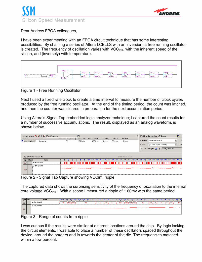
Dear Andrew FPGA colleagues, I have been experimenting with an FPGA circuit technique that has some interesting possibilities. By chaining a series of Altera LCELLS with an inversion, a free running oscillator is created. The frequency of oscillation varies with VCCINT, with the inherent speed of the silicon, and (inversely) with temperature.
Figure 1 - Free Running Oscillator Next I used a fixed rate clock to create a time interval to measure the number of clock cycles produced by the free running oscillator. At the end of the timing period, the count was latched, and then the counter was cleared in preparation for the next accumulation period. Using Altera’s Signal Tap embedded logic analyzer technique; I captured the count results for a number of successive accumulations. The result, displayed as an analog waveform, is shown below.
Figure 2 - Signal Tap Capture showing VCCint ripple The captured data shows the surprising sensitivity of the frequency of oscillation to the internal core voltage VCCINT . With a scope I measured a ripple of ~ 60mv with the same period.
Figure 3 - Range of counts from ripple I was curious if the results were similar at different locations around the chip. By logic locking the circuit elements, I was able to place a number of these oscillators spaced throughout the device, around the borders and in towards the center of the die. The frequencies matched within a few percent.

Layout of LCELLS – The individual circuit elements were manually mapped to specific logic cells so that the timing results would be as identical a possible. The top left LCELL with the floating tool tip shows the left-most NAND gate from Figure – 1 with the seven LCELLS Delay 1, Delay 2, …, Delay7 beneath. The assignments below were used in the assignment editor to fix the cell locations.
Figure 4 – details of LCELL placement Entire Experimental Circuit The complete circuit includes twelve “Silicon Speed” blocks (two shown below), as well as a counter, and a comparator to generate the control signals to start, stop, latch, and clear the count accumulators in each of the twelve measurement blocks. Figure 5 – Entire Circuit
Silicon_Speed:SS6|En_Inv Location LCCOMB_X43_Y18_N0
Silicon_Speed:SS6|delay1 Location LCCOMB_X43_Y18_N2
Silicon_Speed:SS6|delay2 Location LCCOMB_X43_Y18_N4
Silicon_Speed:SS6|delay3 Location LCCOMB_X43_Y18_N6
Silicon_Speed:SS6|delay4 Location LCCOMB_X43_Y18_N8
Silicon_Speed:SS6|delay5 Location LCCOMB_X43_Y18_N10
Silicon_Speed:SS6|delay6 Location LCCOMB_X43_Y18_N12
Silicon_Speed:SS6|delay7 Location LCCOMB_X43_Y18_N14

Silicon Speed Measurement Block Shown here is the detail of each of the measurement blocks with the free running oscillator, a counter, a result latch. Also shown are the control input signals to enable the count period, to latch the result counter, then to clear the counter.
Figure 6 – Details of Speed Measurement Circuit The circuit was crafted to use exactly 32 of the LABs 32 LCELLS Figure 7 – LAB usage Shown below is the location of the twelve Blocks placed within the die. Figure 8 – Placement of Measurement Blocks

Signal Tap Embedded Logic Analyzer Setup The twelve End_Count[7..0] latched outputs of each measurement block is included in the Signal Tap list for capture. The capture size is a 1K samples. Notice that the Buffer Acquisition Mode setting was set to “Segmented” with 1K 1 sample segments. This tells the logic analyzer to capture one sample each time the trigger conditions is meet rather than capturing continuously starting at the trigger point. In this way, a sample is captured each time the accumulated counts are updated.
Figure 9 – Signal Tap Set-up Screen Two captures were collected. One with the device at room temperature, and one with freeze spray applied to the FPGA. The captured results were exported to an Altera *.tbl file which is a text file listing the captured data in column form. This data was then imported into Excel to analyze. A plot (next page) was made from a block of captured data and graphed in Excel. Overlaid on top of this was a screen capture of the ripple seen on the VCCINT. The screen waveform was scaled to show the best match between the two. It is clear that the internal frequency of the free-running oscillator closely tracks the VCCINT. The Vp-p of the ripple was 60mv. The cold freeze spray runs resulted in counts a few percentage points higher than the room temperature runs.
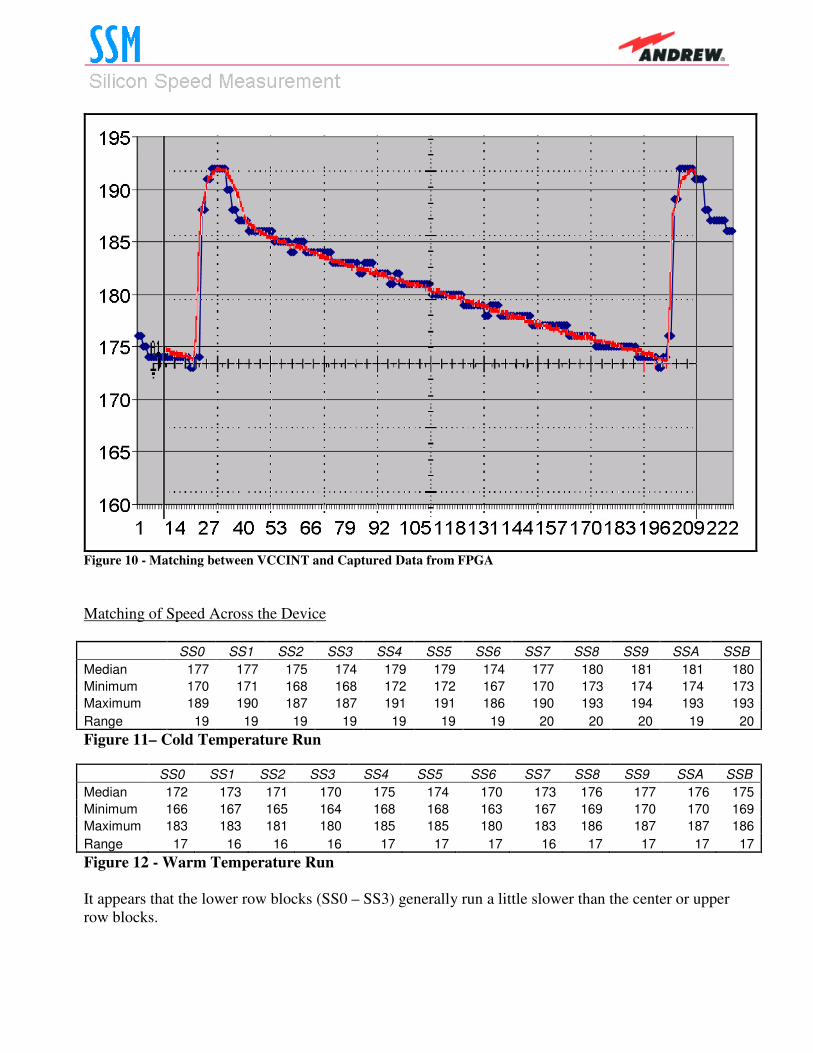
Figure 10 - Matching between VCCINT and Captured Data from FPGA
Matching of Speed Across the Device
SS0 SS1 SS2 SS3 SS4 SS5 SS6 SS7 SS8 SS9 SSA SSB
Median 177 177 175 174 179 179 174 177 180 181 181 180
Minimum 170 171 168 168 172 172 167 170 173 174 174 173
Maximum 189 190 187 187 191 191 186 190 193 194 193 193
Range 19 19 19 19 19 19 19 20 20 20 19 20
Figure 11– Cold Temperature Run
SS0 SS1 SS2 SS3 SS4 SS5 SS6 SS7 SS8 SS9 SSA SSB
Median 172 173 171 170 175 174 170 173 176 177 176 175
Minimum 166 167 165 164 168 168 163 167 169 170 170 169
Maximum 183 183 181 180 185 185 180 183 186 187 187 186
Range 17 16 16 16 17 17 17 16 17 17 17 17
Figure 12 - Warm Temperature Run
It appears that the lower row blocks (SS0 – SS3) generally run a little slower than the center or upper
row blocks.
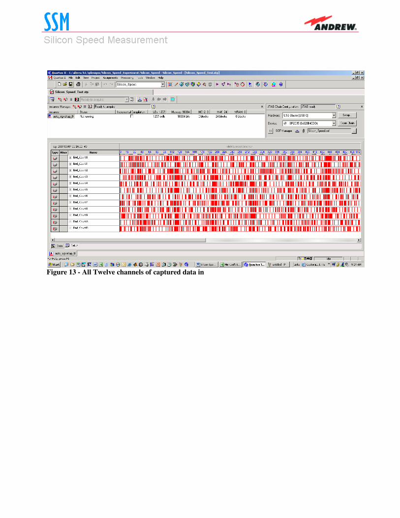
Figure 13 - All Twelve channels of captured data in
Implications In order to maximize their profit, Altera sells faster devices for more money. It is also true that as their foundry evolves the process, and they get a higher percentage of faster devices, they may mark their excess fast devices as slower parts and sell them as slower parts. This is fine except that faster devices dissipate more power, even at slower clock speeds. Faster devices have a higher static current leakage. Since the transistors are biased higher, they switch to the on state more quickly. This means that a design that uses slower devices may be forced to dissipate more power than necessary lowering the end products efficiency. It is also true that slower devices dissipate less power and can possibly have their VCCINT raised to speed up the device. Altera keeps their published voltage tolerances tight, perhaps tighter than they need to so they can both boast of high device speed and lower power dissipation. But even now there is a hint that this window may be opening. Their latest device (Stratix 3) sports a dual mode where VCCINT can be set to either 1.1 VDC or 0.9 VDC depending upon whether one needs to optimize for speed, or for low power. Proposal An external processor read the End_Count value from the FPGA and nudge the VCCINT up or down to bring the internal speed to a specified value. This can be done to either lower the dissipated power or to raise the effective speed of the device. There may be FPGA algorithms that are best operated at the fastest rate possible instead of at a fixed (worst case) rate. These could be run at a rate derived from the free-running oscillator. Next Steps Make runs at calibrated temperatures to understand chip-speed versus temperature. Measure the current during these runs to understand how power dissipation is affected. See to what extent self-heating affects chip-speed. The ultimate goal is to get FPGA makers lower their prices by simplifying the process of matching device to the application; possibly getting them to move VCCINT control onto the chip itself, at the same time easing their speed binning requirements and simplifying power dissipation prediction.