Embed Size (px)
Citation preview

Silicon Sensors for HL-LHC Tracking Detectors - RD50 Status Report
Igor Mandić Jožef Stefan Institute, Ljubljana, Slovenia
On behalf of RD50 collaboration
RD50 – Radiation hard semiconductor devices for very high luminosity colliders
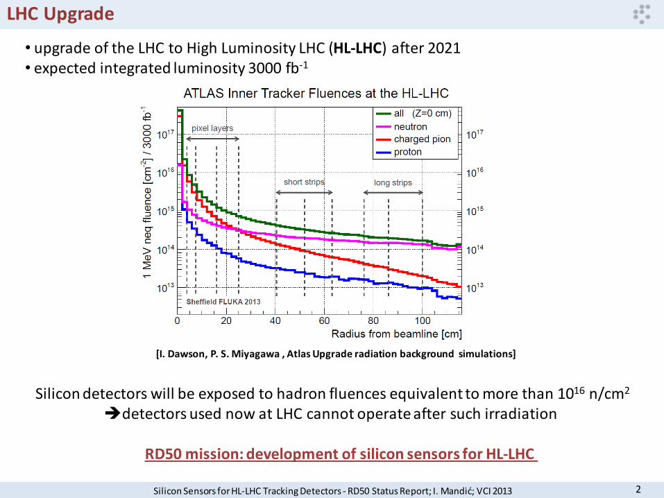
LHC Upgrade
Silicon Sensors for HL-LHC Tracking Detectors - RD50 Status Report; I. Mandić; VCI 2013 2
Silicon detectors will be exposed to hadron fluences equivalent to more than 1016 n/cm2
detectors used now at LHC cannot operate after such irradiation
RD50 mission: development of silicon sensors for HL-LHC
• upgrade of the LHC to High Luminosity LHC (HL-LHC) after 2021 • expected integrated luminosity 3000 fb-1
[I. Dawson, P. S. Miyagawa , Atlas Upgrade radiation background simulations]

RD50 Collaboration
Silicon Sensors for HL-LHC Tracking Detectors - RD50 Status Report; I. Mandić; VCI 2013 3
• RD50: 49 institutes and 263 members
39 European and Asian institutes Belarus (Minsk), Belgium (Louvain), Czech Republic (Prague (3x)),
Finland (Helsinki, Lappeenranta ), France (Paris), Germany (Dortmund, Erfurt, Freiburg, Hamburg, Karlsruhe, Munich), Italy (Bari, Florence, Padova, Perugia, Pisa, Trento), Lithuania (Vilnius),
Netherlands (NIKHEF), Norway (Oslo)), Poland (Krakow, Warsaw(2x)), Romania (Bucharest (2x)), Russia (Moscow, St.Petersburg), Slovenia (Ljubljana), Spain (Barcelona(2x),
Santander, Valencia), Switzerland (CERN, PSI), Ukraine (Kiev), United Kingdom (Glasgow, Liverpool)
8 North-American institutes Canada (Montreal), USA (BNL, Fermilab, New Mexico,
Purdue, Santa Cruz, Syracuse)
1 Middle East institute Israel (Tel Aviv)
1 Asian institute India (Delhi)
Detailed member list: http://cern.ch/rd50

RD50 Collaboration
Silicon Sensors for HL-LHC Tracking Detectors - RD50 Status Report; I. Mandić; VCI 2013 4
Co-Spokespersons Gianluigi Casse and Michael Moll (Liverpool University) (CERN PH-DT)
Defect / Material Characterization
Mara Bruzzi (INFN & Uni Florence)
Detector Characterization
Eckhart Fretwurst (Hamburg University)
Full Detector Systems
Gregor Kramberger (JSI Ljubljana)
Characterization of microscopic properties
of standard-, defect engineered and new materials pre- and
post- irradiation
• WODEAN: Workshop on Defect Analysis in Silicon Detectors (G.Lindstroem & M.Bruzzi)
• Characterization of test structures (IV, CV, CCE, TCT,.)
•Development and testing of defect engineered silicon devices
•EPI, MCZ and other materials •NIEL •Device modeling •Operational conditions •Common irradiations • New Materials (E.Verbitskaya) • Wafer procurement (M.Moll) • Simulations (V.Eremin)
• 3D detectors • Thin detectors • Cost effective solutions • Other new structures
• Semi 3D (Z.Li) •Thinned detectors •Slim Edges (H.Sadrozinski) • Low Resistivty Strips(M. Ullan)
• LHC-like tests • Test beams • Links to HEP • Links electronics R&D • Comparison: - pad-mini-full detectors - different producers
• Pixel Europe (T.Rohe) • Pixel US (D.Bortoletto) • Test beams (G.Casse)
New Structures
Giulio Pellegrini (CNM Barcelona)
Collaboration Board Chair & Deputy: G. Kramberger(Ljubljana) & J.Vaitkus (Vilnius), Conference committee: U.Parzefall (Freiburg) CERN contact: M.Moll (PH-DT), Secretary: V.Wedlake (PH-DT), Budget holder & GLIMOS: M.Glaser (PH-DT)
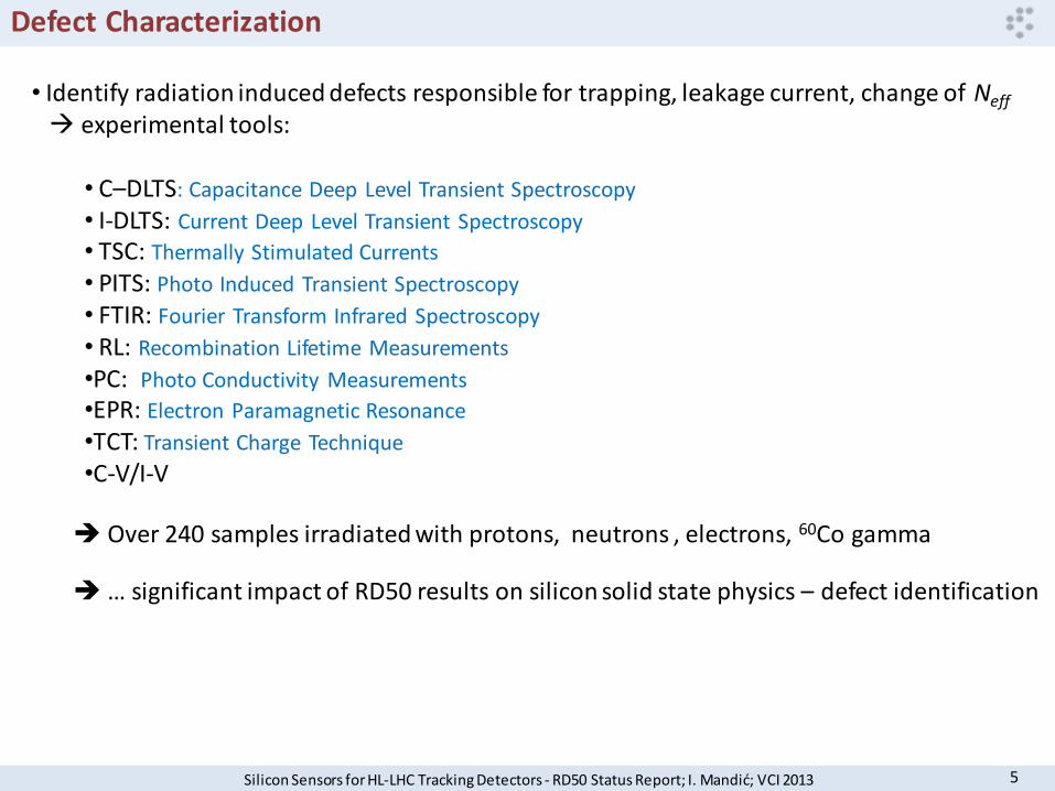
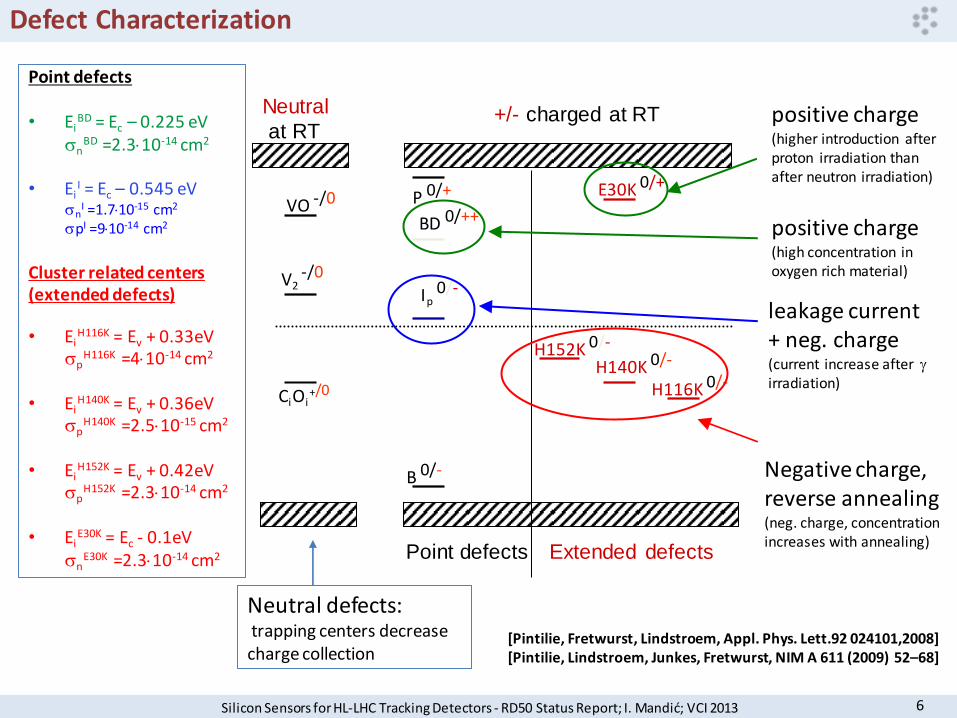
Defect Characterization
Silicon Sensors for HL-LHC Tracking Detectors - RD50 Status Report; I. Mandić; VCI 2013 5
• Identify radiation induced defects responsible for trapping, leakage current, change of Neff experimental tools:
• C–DLTS: Capacitance Deep Level Transient Spectroscopy
• I-DLTS: Current Deep Level Transient Spectroscopy
• TSC: Thermally Stimulated Currents
• PITS: Photo Induced Transient Spectroscopy
• FTIR: Fourier Transform Infrared Spectroscopy
• RL: Recombination Lifetime Measurements
•PC: Photo Conductivity Measurements
•EPR: Electron Paramagnetic Resonance
•TCT: Transient Charge Technique
•C-V/I-V Over 240 samples irradiated with protons, neutrons , electrons, 60Co gamma … significant impact of RD50 results on silicon solid state physics – defect identification
Defect Characterization
Silicon Sensors for HL-LHC Tracking Detectors - RD50 Status Report; I. Mandić; VCI 2013 6
Point defects • Ei
BD = Ec – 0.225 eV n
BD =2.310-14 cm2
• Ei
I = Ec – 0.545 eV n
I =1.710-15 cm2
pI =910-14 cm2
Cluster related centers (extended defects)
• EiH116K = Ev + 0.33eV
pH116K =410-14 cm2
• Ei
H140K = Ev + 0.36eV p
H140K =2.510-15 cm2
• Ei
H152K = Ev + 0.42eV p
H152K =2.310-14 cm2 • Ei
E30K = Ec - 0.1eV n
E30K =2.310-14 cm2
V2 -/0
VO -/0 P 0/+
H152K 0/- H140K 0/-
H116K 0/- CiOi+/0
BD 0/++
Ip 0/-
E30K 0/+
B 0/-
Neutral
at RT +/- charged at RT
Point defects Extended defects
Negative charge, reverse annealing (neg. charge, concentration increases with annealing)
leakage current + neg. charge (current increase after irradiation)
positive charge (higher introduction after proton irradiation than after neutron irradiation)
positive charge (high concentration in oxygen rich material)
[Pintilie, Fretwurst, Lindstroem, Appl. Phys. Lett.92 024101,2008] [Pintilie, Lindstroem, Junkes, Fretwurst, NIM A 611 (2009) 52–68]
Neutral defects: trapping centers decrease charge collection
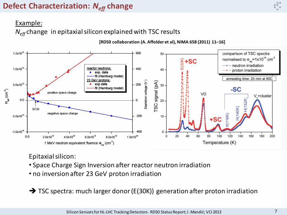
Defect Characterization: Neff change
Silicon Sensors for HL-LHC Tracking Detectors - RD50 Status Report; I. Mandić; VCI 2013 7
Example: Neff change in epitaxial silicon explained with TSC results
Epitaxial silicon: • Space Charge Sign Inversion after reactor neutron irradiation • no inversion after 23 GeV proton irradiation TSC spectra: much larger donor (E(30K)) generation after proton irradiation
[RD50 collaboration (A. Affolder et al), NIMA 658 (2011) 11–16]
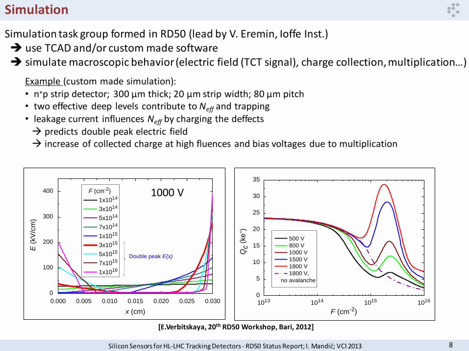
Simulation
Silicon Sensors for HL-LHC Tracking Detectors - RD50 Status Report; I. Mandić; VCI 2013 8
Simulation task group formed in RD50 (lead by V. Eremin, Ioffe Inst.) use TCAD and/or custom made software simulate macroscopic behavior (electric field (TCT signal), charge collection, multiplication…)
1013 1014 1015 10160
5
10
15
20
25
30
35
Qc (
ke- )
F (cm-2)
500 V
800 V
1000 V
1500 V
1800 V
1800 V,
no avalanche
[E.Verbitskaya, 20th RD50 Workshop, Bari, 2012]
0.000 0.005 0.010 0.015 0.020 0.025 0.030
0
100
200
300
400
E (
kV
/cm
)
x (cm)
F (cm-2)
1x10¹⁴
3x10¹⁴
5x10¹⁴
7x10¹⁴
1x10¹⁵
3x10¹⁵
5x10¹⁵
7x10¹⁵
1x10¹⁶
Double peak E(x)
1000 V
Example (custom made simulation): • n+p strip detector; 300 µm thick; 20 µm strip width; 80 µm pitch • two effective deep levels contribute to Neff and trapping • leakage current influences Neff by charging the deffects predicts double peak electric field increase of collected charge at high fluences and bias voltages due to multiplication
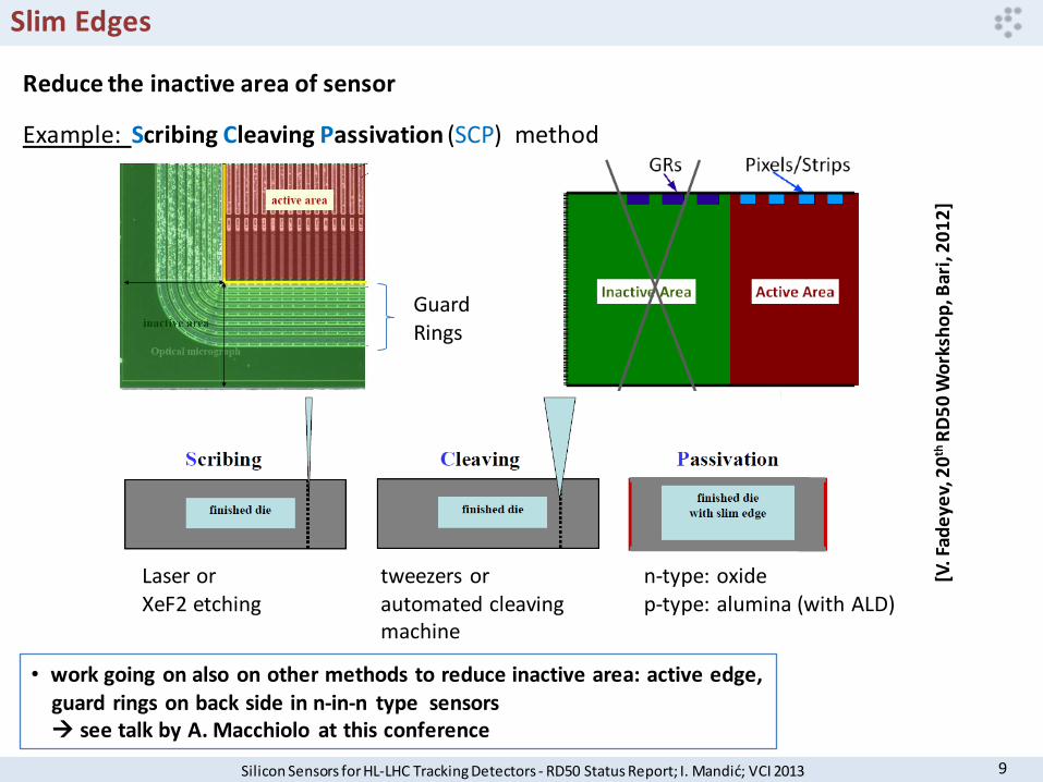
Slim Edges
Silicon Sensors for HL-LHC Tracking Detectors - RD50 Status Report; I. Mandić; VCI 2013 9
[V. F
ade
yev,
20
th R
D5
0 W
ork
sho
p, B
ari,
20
12
]
Reduce the inactive area of sensor
Example: Scribing Cleaving Passivation (SCP) method
Guard Rings
Laser or XeF2 etching
tweezers or automated cleaving machine
n-type: oxide p-type: alumina (with ALD)
• work going on also on other methods to reduce inactive area: active edge, guard rings on back side in n-in-n type sensors see talk by A. Macchiolo at this conference

Edge – Transient Current Technique (Edge-TCT)
Silicon Sensors for HL-LHC Tracking Detectors - RD50 Status Report; I. Mandić; VCI 2013 10
[G. Kramberger, IEEE TNS, VOL. 57, NO. 4, AUGUST 2010, 2294]
• Illuminate segmented sensor from the side with fast (sub-ns), focused (10 µm) infrared laser pulses • Scan across the detector thickness • Record current pulses as function of depth
ns
dttyIyQ
25
0
),()(
)0~,()0~,)(( tyItyvv he
Charge collection profile:
Velocity profile:
G. Kramberger, 17th RD50 Workshop, 2010
Vfd~16 V
p-type Φ = 0
[N.Pacifico, 20th RD50 Workshop, Bari, 2012]
y
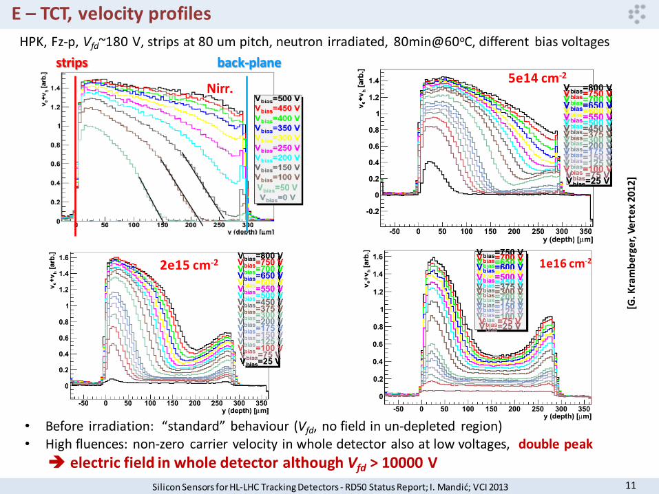
E – TCT, velocity profiles
Silicon Sensors for HL-LHC Tracking Detectors - RD50 Status Report; I. Mandić; VCI 2013 11
HPK, Fz-p, Vfd~180 V, strips at 80 um pitch, neutron irradiated, 80min@60oC, different bias voltages
Nirr. 5e14 cm-2
2e15 cm-2 1e16 cm-2
strips back-plane
• Before irradiation: “standard” behaviour (Vfd, no field in un-depleted region) • High fluences: non-zero carrier velocity in whole detector also at low voltages, double peak
electric field in whole detector although Vfd > 10000 V
[G. K
ram
ber
ger,
Ver
tex
2012
]

Charge Multiplication
Silicon Sensors for HL-LHC Tracking Detectors - RD50 Status Report; I. Mandić; VCI 2013 12
• CCE measured with p-type Si microstrip detectors irradiated to high fluences and biased with high voltages shows evidence of charge multiplication effect: 100% CCE seen after 3x10¹⁵ n/cm2, 15000 electrons after 1016n/cm2
• high negative space charge concentration in detector bulk because of irradiation high electric field close to the n-type strips impact ionization!
Red: calculations based on Neff and trapping measurements at lower fluences Black: measurements At high bias and high fluence: measured >> expected
[RESMDD 2008., I. Mandić et al., NIMA 612 (2010) 474–477]

Charge Multiplication
Silicon Sensors for HL-LHC Tracking Detectors - RD50 Status Report; I. Mandić; VCI 2013 13
Charge Multiplication measured after high levels of irradiation with
different techniques and in several different types of devices
Epi pad (75 µm)
[J. L
ange
et
al.,
NIM
A62
2 (2
010)
49
-58.
]
Φeq = 1e16 cm-2
[M. K
oeh
ler et al., (2011) NIM
A659 272
-281]
3D detector
[A. A
ffold
er et al., (2011) NIM
A658 11
-16]
Test beam
[G. C
asse
et
al.,
NIM
A 6
24
, 2
01
0,
40
1-4
04]
Strip detectors irradiated to Φeq = 5e15 cm-2
90Sr, alibava readout
Full charge for 140 µm thick detector
140 µm
300 µm
Charge(140 µm) > Charge(300 µm) thinner sensors give more charge at very high fluences

Charge multiplication: annealing
Silicon Sensors for HL-LHC Tracking Detectors - RD50 Status Report; I. Mandić; VCI 2013 14
[I. Mandić et al., NIMA629 (2011) 101–105]
Mo
st p
rob
able
ch
arge
[el]
Neff increases with long term annealing collected charge increases at high voltages because of multiplication
SCT128 chip readout
[M. Milovanović et al., 2012 JINST 7 P06007]
E-TCT
Before annealing
After annealing
Increase of collected charge near strips multiplication!
Φeq = 1016 n/cm2

Charge multiplication: enhance the effect
Silicon Sensors for HL-LHC Tracking Detectors - RD50 Status Report; I. Mandić; VCI 2013 15
Junction engineering : • 5 µm wide trench in the middle of the implant • depth of the trench: 5, 10 or 50 µm
[G. Casse et al., NIMA 699 (2013) 9-13]
[G.Casse, Trento Workshop, Feb.2012]
5 µm 50 µm 10 µm
standard
Φeq = 5e15 cm-2
Large effect of 5 µm and 50 µm deep trench after irradiation!
Increased electric field at the trench
[P. Fernandez –Martinez et al., NIMA 658 (2011) 98-102]
Calculation of E field, Φeq = 0.
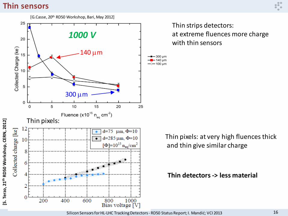
Thin sensors
Silicon Sensors for HL-LHC Tracking Detectors - RD50 Status Report; I. Mandić; VCI 2013 16
Thin strips:
1000 V
Thin pixels: at very high fluences thick and thin give similar charge
[G.Casse, 20th RD50 Workshop, Bari, May 2012]
1000 V
300 mm
140 mm
Thin pixels:
Thin strips detectors: at extreme fluences more charge with thin sensors
[S.
Terz
o, 2
1th R
D50
Wo
rksh
op
, CER
N, 2
012]
Thin detectors -> less material
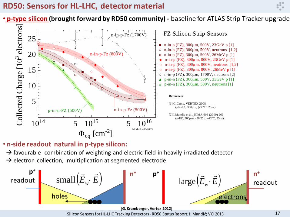
RD50: Sensors for HL-LHC, detector material
Silicon Sensors for HL-LHC Tracking Detectors - RD50 Status Report; I. Mandić; VCI 2013 17
1014 5 1015 5 1016
eq [cm-2]
5
10
15
20
25
Coll
ecte
d C
har
ge
[10
3 e
lect
rons]
n-in-p (FZ), 300mm, 500V, 23GeV p [1]
n-in-p (FZ), 300mm, 500V, neutrons [1,2]
n-in-p (FZ), 300mm, 500V, 26MeV p [1]
n-in-p (FZ), 300mm, 800V, 23GeV p [1]
n-in-p (FZ), 300mm, 800V, neutrons [1,2]
n-in-p (FZ), 300mm, 800V, 26MeV p [1]
n-in-p-Fz (500V)
n-in-p-Fz (800V)
n-in-p-Fz (1700V)
n-in-p (FZ), 300mm, 1700V, neutrons [2]
p-in-n (FZ), 300mm, 500V, 23GeV p [1]
p-in-n (FZ), 300mm, 500V, neutrons [1]
p-in-n-FZ (500V)
M.Moll - 09/2009
References:
[1] G.Casse, VERTEX 2008
(p/n-FZ, 300mm, (-30oC, 25ns)
[2] I.Mandic et al., NIMA 603 (2009) 263
(p-FZ, 300mm, -20oC to -40oC, 25ns)
[3] n/n-FZ, 285mm, (-10oC, 40ns), pixel [Rohe et al. 2005][1] 3D, double sided, 250mm columns, 300mm substrate [Pennicard 2007][2] Diamond [RD42 Collaboration][3] p/n-FZ, 300mm, (-30oC, 25ns), strip [Casse 2008]
FZ Silicon Strip Sensors
• p-type silicon (brought forward by RD50 community) - baseline for ATLAS Strip Tracker upgrade
holes
EEw
small
• n-side readout natural in p-type silicon: favourable combination of weighting and electric field in heavily irradiated detector electron collection, multiplication at segmented electrode
p+
readout n+
EEw
large
electrons
n+
readout p+
[G. Kramberger, Vertex 2012]
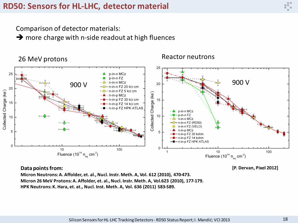
RD50: Sensors for HL-LHC, detector material
Silicon Sensors for HL-LHC Tracking Detectors - RD50 Status Report; I. Mandić; VCI 2013 18
26 MeV protons
900 V 900 V
Reactor neutrons
Comparison of detector materials: more charge with n-side readout at high fluences
Data points from: Micron Neutrons: A. Affolder, et. al., Nucl. Instr. Meth. A, Vol. 612 (2010), 470-473. Micron 26 MeV Protons: A. Affolder, et. al., Nucl. Instr. Meth. A, Vol.623 (2010), 177-179. HPK Neutrons: K. Hara, et. at., Nucl. Inst. Meth. A, Vol. 636 (2011) S83-S89.
[P. Dervan, Pixel 2012]

RD50: Sensors for HL-LHC, detector material
Silicon Sensors for HL-LHC Tracking Detectors - RD50 Status Report; I. Mandić; VCI 2013 19
• n-MCz (introduced by RD50 community) might improve performance in mixed fields due to compensation of neutron and charged particle damage interesting in mixed radiation field p-in-n MCz detectors interesting also because of lower cost
[G. K
ram
be
rge
r e
t al
. NIM
A 6
09
(2
00
9)
14
2–1
48]
Damage done by 24 GeV protons or 300 MeV pions compensated with damage caused by neutrons
J. M
etc
alfe
, M. H
oe
ferk
amp
, S. S
eid
el
n-MCz less affected by annealing
(800 MeV protons)
• CCE > 50% at 500 V with p-in-n–type MCz detectors after eq=1e15 cm-2 (26 MeV p) [E. Tuovinen et al., NIMA 636 (2011) S39]
more about MCz and Epi material in talk by A. Junkes

RD50: Sensors for HL-LHC, device type
Silicon Sensors for HL-LHC Tracking Detectors - RD50 Status Report; I. Mandić; VCI 2013 20
Planar segmented detectors n-in-p or n-in-n results on highly irradiated planar segmented sensors have shown that these devices are a feasible option for the innermost layers of LHC upgrade
More about planar pixel results in the talk by A. Macchiolo!
[S. T
erz
o, 2
1th
RD
50
Wo
rksh
op
, CE
RN
, 20
12
]
Example: • 285 µm thick n-in-p FZ pixels • FE-I3 readout • sufficient charge also at Φeq = 1·1016 n/cm2
Φeq = 1·1016 n/cm2 • test beam, 120 GeV pions: • perpendicular beam incidence • bias voltage: 600V • threshold: 2000 el
97.2% hit efficiency (98.1% in the central region)
RD50: Sensors for HL-LHC, device type
Silicon Sensors for HL-LHC Tracking Detectors - RD50 Status Report; I. Mandić; VCI 2013 21
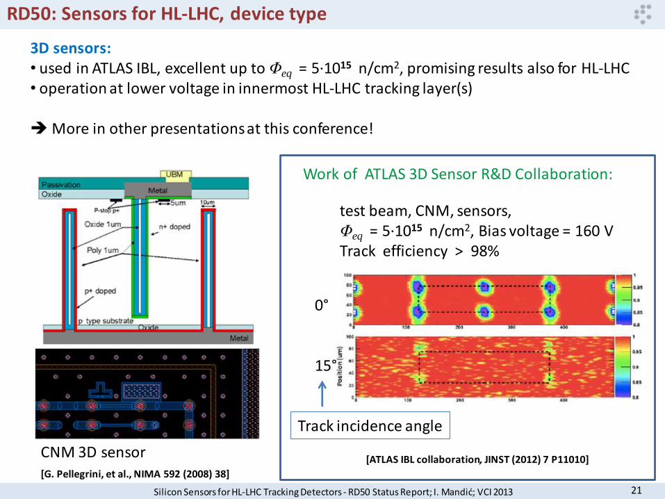
3D sensors: • used in ATLAS IBL, excellent up to Φeq = 5·1015 n/cm2, promising results also for HL-LHC • operation at lower voltage in innermost HL‐LHC tracking layer(s) More in other presentations at this conference!
test beam, CNM, sensors, Φeq = 5·1015 n/cm2, Bias voltage = 160 V Track efficiency > 98%
0° 15°
Track incidence angle
Work of ATLAS 3D Sensor R&D Collaboration:
CNM 3D sensor [G. Pellegrini, et al., NIMA 592 (2008) 38]
[ATLAS IBL collaboration, JINST (2012) 7 P11010]
Conclusion
Silicon Sensors for HL-LHC Tracking Detectors - RD50 Status Report; I. Mandić; VCI 2013 22
RD50 recommendations for the silicon detectors to be used for LHC detector upgrades:
Innermost layers: fluences up to 2·1016 neq /cm2
• present results show that planar sensors are good enough readout on n-type electrode is essential! n-in-p (or n-in-n becoming n-in-p after inversion) detectors
• need high bias voltage , but may be less demanding with thin sensors • 3D detectors promising lower bias voltage
• may be more difficult to produce but IBL results are encouraging Outer layers: fluences up to 1015 n/cm-2
• n-in-p type FZ microstrip detectors are ATLAS baseline: Collected charge over 104 electrons at 500 V (over 1.5·104 el. at 900 V) • p-in-n MCz detectors possible option exploit damage compensation in mixed radiation field lower cost Research with all types of material: FZ, MCz and Epi still going on
Thank you!
Silicon Sensors for HL-LHC Tracking Detectors - RD50 Status Report; I. Mandić; VCI 2013 23
RD50 is a large and active collaboration! only very limited selection of results included in this presentation please visit www.cern.ch/rd50 for more information

Defect Characterization: carrier de-trapping
Silicon Sensors for HL-LHC Tracking Detectors - RD50 Status Report; I. Mandić; VCI 2013 24
De
trap
pe
d c
har
ge [a
rb.]
Standard TCT setup: illuminate with short red laser pulse record time resolved pulse integrate the pulse subtract (measured) response curve fit with 2 exponentials
-110 V
'
0
')()( dttItQ
t
Φeq= 1e14 n/cm2 T = 25°C
de-trapping times for holes are in the range from 1-10 µs, the long term dominates de-trapping times of electrons are larger than ~10 µs not investigated in this measurement
[G.K
ram
ber
ger
et a
l., 2
012
JIN
ST 7
P04
006
]
[G.K
ram
ber
ger
et a
l., 1
8th
RD
50 W
ork
sho
p L
iver
po
ol ]
Se
e a
lso
[M.
Gab
rysh
, 20t
h R
D50
Wo
rksh
op
, Bar
i]
measure at different temperatures estimate trap parameters
H152K H140K,H116K
Φeq= 1e14 n/cm2 Trap σh (cm-2
) Et (eV)
H1(short τ) (3±2)·10-13
0.44±0.04
H2(long τ) (5±5)·10-16
0.355±0.04