Embed Size (px)
Citation preview
Silicate and direct bonding of low thermal expansion materials
Gerhard Kalkowski*a, Simone Fabiana, Carolin Rothhardtb, Paul Zellerc, and Stefan Rissea
a Fraunhofer Institut für Angewandte Optik und Feinmechanik, 07745 Jena, Germany b Institut für Angewandte Physik, Friedrich Schiller Universität, 07745 Jena, Germany
c Astrium GmbH, 81663 München, Germany
ABSTRACT
Joining of materials becomes an issue, when high stability at large temperature variation is required. Stress from thermal mismatch of auxiliary materials and corresponding distortions are often unavoidable. We describe the use of two inorganic bonding technologies for joining low thermal expansion glasses. The techniques of silicate and direct bonding were applied to join ultra-low thermal expansion glass elements of 150 mm diameter to from light-weight and high precision opto-mechanical compounds. Related bond strengths were investigated on separate reference specimen. Dimensional stability of the bonded systems during thermal cycling in vacuum was investigated by Fizeau interferometry at temperatures between 78 K and 335 K with high accuracy. The results illustrate the great potential of both bonding technologies for glass based precision engineering applications to be used under highly demanding environmental conditions, like in space. Keywords: glass joining, silicate bonding, direct bonding, ultra-low expansion glass, thermal stability, interferometry
1. INTRODUCTION
Low thermal expansion materials, like fused silica with a coefficient of thermal expansion (CTE) of about 50*10-8/K at room temperature, or dedicated ultra-low (“zero”) expansion materials like ULE glass (from Corning) and ZERODUR glass-ceramics (from Schott) with CTEs of about 2*10-8/K are key materials in optics and high precision mechanics. Fused silica dominates UV-VIS transmission optics, and ULE and ZERODUR are common materials for reflective optics in astronomy and modern lithography, as well as high precision mechanical devices. Stable joining of these materials with adhesives –although simple and fast– leads to problems in applications where thermal variations occur. The huge CTE of adhesives –typically of the order of 50*10-6/K– and the disposition to creep under load are extremely undesirable properties. Low temperature soldering would be an alternative, but local stresses are unavoidable there. When materials adapted joints of high stiffness and stability among similar glass materials are required, silicate or direct bonding may be the better choice. Both technologies rely on initially humid surface conditions and require a final annealing step at low to moderate temperatures to establish permanent bonds. Silicate bonding involves the use of water based solutions of alkali silicates as a low viscosity additive for joining silicate glasses. The underlying mechanism consists of an initial etching reaction at the glass surfaces and subsequent re-solidification, with the generation of a complex connecting network of covalent Si-O-Si bonds between the bonded parts1. By contrast, direct bonding works without explicit additives on extremely smooth and hydrophilic surfaces, using just adsorbed water molecules from the environment2. The technology traces back to the method of “optical contacting” of extremely flat and polished optical surfaces and leads to similar covalent Si-O-Si bonds as silicate bonding, if the surfaces are sufficiently smooth and conform. Although originating in optics, this refined technology is currently not much applied to optical materials. We have recently explored direct bonding of ULE as well as fused silica for precision opto-mechanical and diffractive applications, respectively3,4. In particular, a light-weight ULE demonstrator (Type#1) of 150 mm diameter and about 23 mm height was obtained by “sandwich bonding” of two 1.5 mm thick glass wafers to both sides of a plane-parallel core substrate with bore holes3. If curved shapes are involved, silicate bonding appears more reasonable, in view of less stringent requirements for shape conformity, due to the gap filling nature of the silicate solution. We now apply silicate bonding to join spherically shaped ULE glass elements of 150 mm diameter to each other, which is the largest dimension of non-planar parts bonded with this technology, to our knowledge. A similar “light weight” core substrate was used,
* E-mail address of corresponding author: [email protected] .de
Material Technologies and Applications to Optics, Structures, Components, and Sub-Systems, edited by Joseph L. Robichaud, Matthias Krödel, William A. Goodman, Proc. of SPIE Vol. 8837,
88370U · © 2013 SPIE · CCC code: 0277-786X/13/$18 · doi: 10.1117/12.2022845
Proc. of SPIE Vol. 8837 88370U-1
Downloaded From: http://spiedigitallibrary.org/ on 10/11/2013 Terms of Use: http://spiedl.org/terms
..../i0:::
Fraunhofer -titutAn. e',va ndte ')und ''einmech nik
1111=ma I I IVA 1,1 III 11:A7 I IF
now provided with a spherical surface of radius 750 mm on one side and a plane surface on the back side, to generate a new ULE demonstrator (Type#2). The weight of the core substrate is reduced to about 60% of a massive plate by use of the bore holes. To the spherical concave side of the core substrate, an ULE substrate of corresponding convex shape was attached by silicate bonding. The plane back side of the core substrate was then closed by direct bonding of an ULE wafer. We describe the two bonding technologies and report on the deformation behavior of both compounds (Type#1 and Type#2) upon thermal cycling in vacuum. The large sample diameter is expected to allow sensitive monitoring of strain effects from bonding induced inhomogeneities in the compounds. Using an interferometer set-up, the surface planarity of the two demonstrators was measured at temperatures between about 78 K and 335 K.
2. SILICATE BONDING
Silicate bonding is based on the dissolution of silicates in alkaline solutions around values of pH>11. Originally investigated for bonding of oxidized silicon (Si) wafers5, it proved highly useful for optics and is currently used for telescopes in space6 as well as gravitational waves detectors7. Sometimes also known as hydroxide catalysis bonding, it involves water based solutions of AOH with/out A2SiO4, where A is an alkali metal6, to obtain mineral bonds of high stiffness. The solution may involve additional ingredients8 to rise joining time or bond flexibility, the latter typically by generating non-bridging oxygen sites9. The alkaline solution initially etches the glass surfaces and brings additional silica into solution in the form of ionic Si(OH)n
- complexes. With increasing Si(OH)n- content and subsequent withdrawal of
water, a complex silicate network develops and bonds the parts together. In a simplified way, the basic bonding reaction can be described by the equation1,6: X–Si–OH + OH–Si–X → X–Si–O–Si–X + H2O ↑ (1) Here X stands for the supplemental OH-groups of the Si(OH)n
- ions (n = 4…5) in silicate solution or the bulk environment of the top layer at the glass surface. In our current practice, a water based sodium-silicate solution of OH molarity ≈1 is supplemented with minor amounts of additional ingredients to attain a pH value >12 for the bonding solution. The parts to be bonded are provided with plane or otherwise conform and polished surfaces of moderate roughness (<10 nm root-mean-square (RMS)). Immediately before bonding, all parts are carefully cleaned in a multi stage bath process using ultrasonic agitated surfactants and/or the RCA-1 process10, flushed with deionized water and dried. The resulting surfaces are highly hydrophilic as verified by measuring water wetting angles <10 degrees.
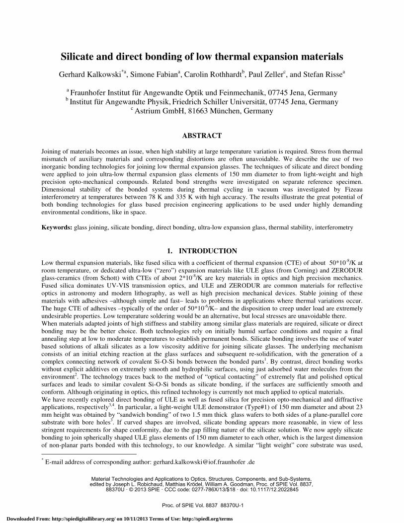
Figure 1: Silicate bonding of 25 mm diameter glass blanks. From left to right: B270, SiO2, ZERODUR, ULE, BK7. For small dimension samples, the silicate solution is simply dropped on one of the samples and the other one is fit above with some additional weight, to squeeze the liquid out of the bonding zone and attain close contact between both parts. At compressive pressures of several kPa in general, the contacted parts are left at rest and dried at ambient conditions for about a week initially. Then curing in vacuum is added, with temperatures slowly rising from room temperature to above 100°C finally, to extract the water from the bonding zone and promote the condensation reaction according to equation 1. The thickness of the bonding zone depends on sample size and bonding conditions and is of the order of 100 nm to several 100 nm typically1,6. High transparency bonds can be achieved this way and the technology is rather
Proc. of SPIE Vol. 8837 88370U-2
Downloaded From: http://spiedigitallibrary.org/ on 10/11/2013 Terms of Use: http://spiedl.org/terms
universally applicable to different glass materials as visible in Fig. 1 for blanks of 25 mm diameter of various materials. Silicate bonds withstand extreme temperature gradients. In fact, bonded fused silica glass blanks were immersed into liquid Nitrogen from room temperature and could be retrieved without damage.
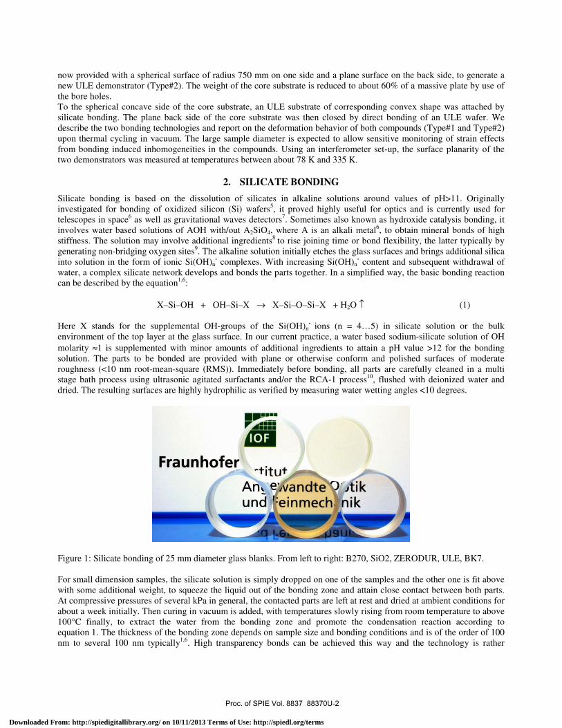
Figure 2: Set-up for 3-point bending test Figure 3: Bonding strengths obtained by silicate bonding (left) und corresponding values for similarly cut bulk material (right) Quantitative values for the bond strength were obtained from 3-point bending tests on rectangular beams cut out of the bonded samples with a diamond saw. The test procedure is displayed in Fig. 2 and involves the measurement of the force (F) at the instant of fracture in addition to height (h), width (b) and length (l) of the sample between the lines of support. The fracture stresses (σ) are calculated according to the formula11
σ = 3 F l / (2 b h²) (2) and displayed in Fig. 3 for several bonded samples (at left) as well as massive bulk reference samples (at right) cut the same way. The data represent the arithmetic mean and the standard deviations for samples of at least 5 beams cut from a pair of bonded blanks. Apparently, the bonding strength of silicate bonding amounts to about 50 % or more of the bulk materials. Note, that also glass blanks with various dielectric thin film coatings have been bonded this way, although the bonding strength is significantly reduced as compared to uncoated samples12.
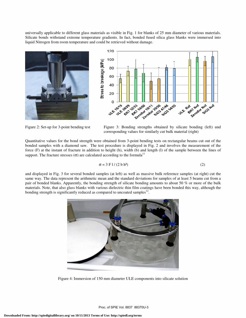
Figure 4: Immersion of 150 mm diameter ULE components into silicate solution
Proc. of SPIE Vol. 8837 88370U-3
Downloaded From: http://spiedigitallibrary.org/ on 10/11/2013 Terms of Use: http://spiedl.org/terms
51007_2010-08-26_
Upon contacting larger parts this way, the wetting front of the solution at the glass surfaces becomes locally unstable and air bubbles tend to be enclosed in the bonding zone. The better choice is then to float the surfaces to be bonded by immersion into a container with the silicate solution. Fig. 4 illustrates this approach for the silicate bonding procedure applied to bond the spherically shaped surfaces of our 150 mm diameter Type#2 ULE demonstrator. First, the convex cover plate is immersed into the liquid. Then the core substrate (held by vacuum grippers in Fig. 7) is immersed to wet the bonding surface for a few minutes, before it is deposited above the cover plate.
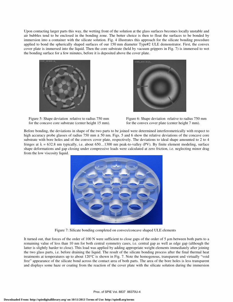
Figure 5: Shape deviation relative to radius 750 mm Figure 6: Shape deviation relative to radius 750 mm for the concave core substrate (center height 15 mm). for the convex cover plate (center height 7 mm).
Before bonding, the deviations in shape of the two parts to be joined were determined interferometrically with respect to high accuracy probe glasses of radius 750 mm ± 50 nm. Figs. 5 and 6 show the relative deviations of the concave core substrate with bore holes and of the convex cover plate, respectively. The deviations to ideal shape amounted to 2 to 4 fringes at λ = 632.8 nm typically, i.e. about 650…1300 nm peak-to-valley (PV). By finite element modeling, surface shape deformations and gap closing under compressive loads were calculated at zero friction, i.e. neglecting minor drag from the low viscosity liquid.
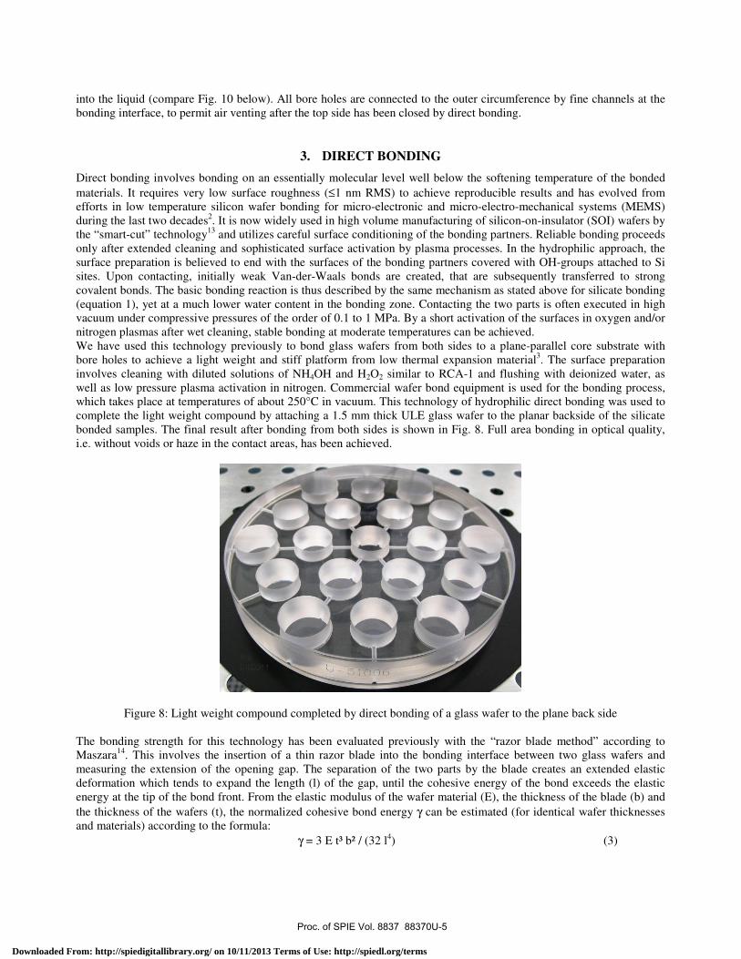
Figure 7: Silicate bonding completed on convex/concave shaped ULE elements
It turned out, that forces of the order of 100 N were sufficient to close gaps of the order of 5 µm between both parts to a remaining value of less than 10 nm for both central symmetry cases, i.e. central gap as well as edge gap (although the latter is slightly harder to close). This load was applied by adding appropriate weight elements immediately after joining the two glass parts, i.e. before draining the liquid. The result of the silicate bonding process after the final thermal heat treatments at temperatures up to about 120°C is shown in Fig. 7. Note the homogenous, transparent und virtually “void free” appearance of the silicate bond across the contact area of both parts. The area of the bore holes is less transparent and displays some haze or coating from the reaction of the cover plate with the silicate solution during the immersion
Proc. of SPIE Vol. 8837 88370U-4
Downloaded From: http://spiedigitallibrary.org/ on 10/11/2013 Terms of Use: http://spiedl.org/terms
a
into the liquid (compare Fig. 10 below). All bore holes are connected to the outer circumference by fine channels at the bonding interface, to permit air venting after the top side has been closed by direct bonding.
3. DIRECT BONDING
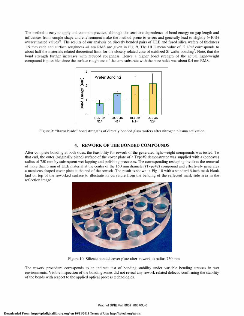
Direct bonding involves bonding on an essentially molecular level well below the softening temperature of the bonded materials. It requires very low surface roughness (≤1 nm RMS) to achieve reproducible results and has evolved from efforts in low temperature silicon wafer bonding for micro-electronic and micro-electro-mechanical systems (MEMS) during the last two decades2. It is now widely used in high volume manufacturing of silicon-on-insulator (SOI) wafers by the “smart-cut” technology13 and utilizes careful surface conditioning of the bonding partners. Reliable bonding proceeds only after extended cleaning and sophisticated surface activation by plasma processes. In the hydrophilic approach, the surface preparation is believed to end with the surfaces of the bonding partners covered with OH-groups attached to Si sites. Upon contacting, initially weak Van-der-Waals bonds are created, that are subsequently transferred to strong covalent bonds. The basic bonding reaction is thus described by the same mechanism as stated above for silicate bonding (equation 1), yet at a much lower water content in the bonding zone. Contacting the two parts is often executed in high vacuum under compressive pressures of the order of 0.1 to 1 MPa. By a short activation of the surfaces in oxygen and/or nitrogen plasmas after wet cleaning, stable bonding at moderate temperatures can be achieved. We have used this technology previously to bond glass wafers from both sides to a plane-parallel core substrate with bore holes to achieve a light weight and stiff platform from low thermal expansion material3. The surface preparation involves cleaning with diluted solutions of NH4OH and H2O2 similar to RCA-1 and flushing with deionized water, as well as low pressure plasma activation in nitrogen. Commercial wafer bond equipment is used for the bonding process, which takes place at temperatures of about 250°C in vacuum. This technology of hydrophilic direct bonding was used to complete the light weight compound by attaching a 1.5 mm thick ULE glass wafer to the planar backside of the silicate bonded samples. The final result after bonding from both sides is shown in Fig. 8. Full area bonding in optical quality, i.e. without voids or haze in the contact areas, has been achieved.
Figure 8: Light weight compound completed by direct bonding of a glass wafer to the plane back side
The bonding strength for this technology has been evaluated previously with the “razor blade method” according to Maszara14. This involves the insertion of a thin razor blade into the bonding interface between two glass wafers and measuring the extension of the opening gap. The separation of the two parts by the blade creates an extended elastic deformation which tends to expand the length (l) of the gap, until the cohesive energy of the bond exceeds the elastic energy at the tip of the bond front. From the elastic modulus of the wafer material (E), the thickness of the blade (b) and the thickness of the wafers (t), the normalized cohesive bond energy γ can be estimated (for identical wafer thicknesses and materials) according to the formula:
γ = 3 E t³ b² / (32 l4) (3)
Proc. of SPIE Vol. 8837 88370U-5
Downloaded From: http://spiedigitallibrary.org/ on 10/11/2013 Terms of Use: http://spiedl.org/terms
The method is easy to apply and common practice, although the sensitive dependence of bond energy on gap length and influences from sample shape and environment make the method prone to errors and generally lead to slightly (≈10%) overestimated values15. The results of our analysis on directly bonded pairs of ULE and fused silica wafers of thickness 1.5 mm each and surface roughness ≈1 nm RMS are given in Fig. 9. The ULE mean value of 2 J/m² corresponds to about half the materials related theoretical limit for the closely related case of oxidized Si wafer bonding2. Note, that the bond strength further increases with reduced roughness. Hence a higher bond strength of the actual light-weight compound is possible, since the surface roughness of the core substrate with the bore holes was about 0.4 nm RMS.
Figure 9: “Razor blade” bond strengths of directly bonded glass wafers after nitrogen plasma activation
4. REWORK OF THE BONDED COMPOUNDS
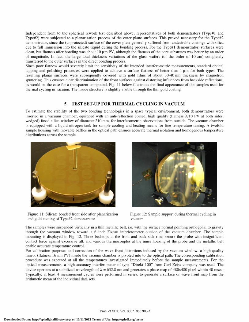
After complete bonding at both sides, the feasibility for rework of the generated light-weight compounds was tested. To that end, the outer (originally plane) surface of the cover plate of a Type#2 demonstrator was supplied with a (concave) radius of 750 mm by subsequent wet lapping and polishing processes. The corresponding reshaping involves the removal of more than 3 mm of ULE material at the center of the 150 mm diameter (Type#2) compound and effectively generates a meniscus shaped cover plate at the end of the rework. The result is shown in Fig. 10 with a standard 6 inch mask blank laid on top of the reworked surface to illustrate its curvature from the bending of the reflected mask side area in the reflection image.
Figure 10: Silicate bonded cover plate after rework to radius 750 mm The rework procedure corresponds to an indirect test of bonding stability under variable bending stresses in wet environments. Visible inspection of the bonding zones did not reveal any rework related defects, confirming the stability of the bonds with respect to the applied optical process technologies.
Proc. of SPIE Vol. 8837 88370U-6
Downloaded From: http://spiedigitallibrary.org/ on 10/11/2013 Terms of Use: http://spiedl.org/terms
Independent from to the spherical rework test described above, representatives of both demonstrators (Type#1 and Type#2) were subjected to a planarization process of the outer plane surfaces. This proved necessary for the Type#2 demonstrator, since the (unprotected) surface of the cover plate generally suffered from undesirable coatings with silica due to full immersion into the silicate liquid during the bonding process. For the Type#1 demonstrator, surfaces were clean, but flatness after bonding was about 10 µm PV, although the flatness of the core substrates was better by an order of magnitude. In fact, the large total thickness variations of the glass wafers (of the order of 10 µm) completely transferred to the outer surfaces in the direct bonding process. Since poor flatness would severely limit the sensitivity of the intended interferometric measurements, standard optical lapping and polishing processes were applied to achieve a surface flatness of better than 1 µm for both types. The resulting planar surfaces were subsequently covered with gold films of about 30-40 nm thickness by magnetron sputtering. This ensures clear discrimination of the front surfaces against distorting influences from backside reflections, as would be the case for a transparent compound. Fig. 11 below illustrates the final appearance of the samples used for thermal cycling in vacuum. The inside structure is slightly visible through the thin gold coating.
5. TEST SET-UP FOR THERMAL CYCLING IN VACUUM
To estimate the stability of the two bonding technologies in a space typical environment, both demonstrators were inserted in a vacuum chamber, equipped with an anti-reflection coated, high quality (flatness λ/10 PV at both sides, wedged) fused silica window of diameter 210 mm, for interferometric observations from outside. The vacuum chamber is equipped with a liquid nitrogen tank for sample cooling and heating means for fine temperature tuning. A twofold sample housing with movable baffles in the optical path ensures accurate thermal isolation and homogenous temperature distributions across the sample.
Figure 11: Silicate bonded front side after planarization Figure 12: Sample support during thermal cycling in and gold coating of Type#2 demonstrator vacuum
The samples were suspended vertically in a thin metallic belt, i.e. with the surface normal pointing orthogonal to gravity through the vacuum window toward a 6 inch Fizeau interferometer outside of the vacuum chamber. The sample mounting is displayed in Fig. 12. Three bedstops at the front and back side rims secure the probe with insignificant contact force against excessive tilt, and various thermocouples at the inner housing of the probe and the metallic belt enable accurate temperature control. For calibration purposes and correction of the wave front distortions induced by the vacuum window, a high quality mirror (flatness 16 nm PV) inside the vacuum chamber is pivoted into to the optical path. The corresponding calibration procedure was executed at all the temperatures investigated immediately before the sample measurements. For the optical measurements, a high accuracy interferometer of type “Direkt 100” from Carl Zeiss company was used. The device operates at a stabilized wavelength of λ = 632.8 nm and generates a phase map of 480x480 pixel within 40 msec. Typically, at least 4 measurement cycles were performed in series, to generate a surface or wave front map from the arithmetic mean of the individual data sets.
Proc. of SPIE Vol. 8837 88370U-7
Downloaded From: http://spiedigitallibrary.org/ on 10/11/2013 Terms of Use: http://spiedl.org/terms
Irms 0.159 Nm I
PV 0. 720 Nm IIP er 0.554 Nm
IAStMaq 0.077 Nm I
Trim: OI
Removed: PST TLT
+405.00
Peak
nm
Valley
-318.00Filter: Off 1
Irms 0.163 Nm I
PV 0.69 Nm IIP er 0.568 Nm
IAStMaq 0.078 Nm I
+405.00
Trim: OI
Removed: PST TLT
Peak
nm
Valley
-318.00Filter: Off 1
6. THERMAL CYCLING IN VACUUM: SILICATE BOND (TYPE#2)
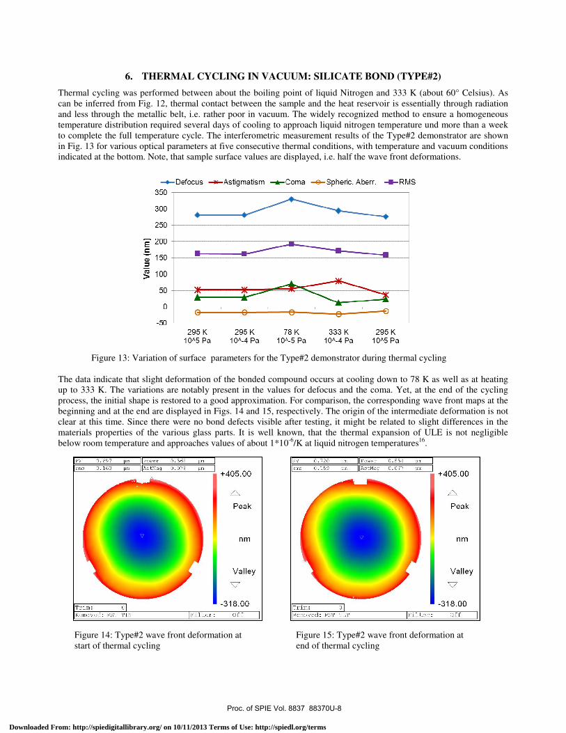
Thermal cycling was performed between about the boiling point of liquid Nitrogen and 333 K (about 60° Celsius). As can be inferred from Fig. 12, thermal contact between the sample and the heat reservoir is essentially through radiation and less through the metallic belt, i.e. rather poor in vacuum. The widely recognized method to ensure a homogeneous temperature distribution required several days of cooling to approach liquid nitrogen temperature und more than a week to complete the full temperature cycle. The interferometric measurement results of the Type#2 demonstrator are shown in Fig. 13 for various optical parameters at five consecutive thermal conditions, with temperature and vacuum conditions indicated at the bottom. Note, that sample surface values are displayed, i.e. half the wave front deformations.
Figure 13: Variation of surface parameters for the Type#2 demonstrator during thermal cycling
The data indicate that slight deformation of the bonded compound occurs at cooling down to 78 K as well as at heating up to 333 K. The variations are notably present in the values for defocus and the coma. Yet, at the end of the cycling process, the initial shape is restored to a good approximation. For comparison, the corresponding wave front maps at the beginning and at the end are displayed in Figs. 14 and 15, respectively. The origin of the intermediate deformation is not clear at this time. Since there were no bond defects visible after testing, it might be related to slight differences in the materials properties of the various glass parts. It is well known, that the thermal expansion of ULE is not negligible below room temperature and approaches values of about 1*10-6/K at liquid nitrogen temperatures16.
Figure 14: Type#2 wave front deformation at Figure 15: Type#2 wave front deformation at start of thermal cycling end of thermal cycling
Proc. of SPIE Vol. 8837 88370U-8
Downloaded From: http://spiedigitallibrary.org/ on 10/11/2013 Terms of Use: http://spiedl.org/terms
Irms 0.026 pm I
PV 0. 129 Nm IIP0 er 0.067 m
IAStMag 0.062 pm
Trim: 01
Removed: PST TLT
+69.00
Peak
nm
Valley
0-81.00
(Filter: Off
Irms 0.028 pm I IAStMaq 0.041 pm I
Pv 0. 150 Nm IIP er 0.081 Nm
Trim: 01
Removed: PST TLT
+69.00
Peak
nm
Valley
-81.00(Filter: Off
7. THERMAL CYCLING IN VACUUM: DIRECT BOND (TYPE#1)
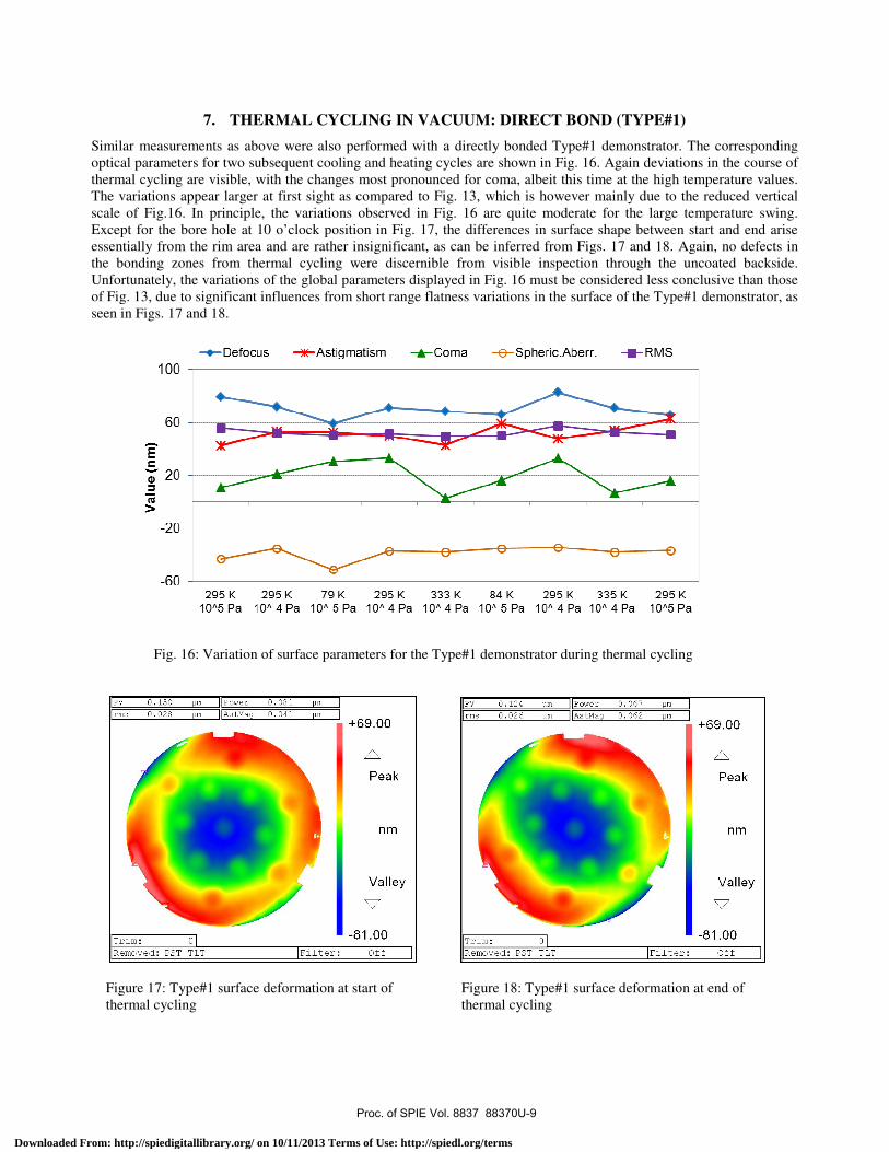
Similar measurements as above were also performed with a directly bonded Type#1 demonstrator. The corresponding optical parameters for two subsequent cooling and heating cycles are shown in Fig. 16. Again deviations in the course of thermal cycling are visible, with the changes most pronounced for coma, albeit this time at the high temperature values. The variations appear larger at first sight as compared to Fig. 13, which is however mainly due to the reduced vertical scale of Fig.16. In principle, the variations observed in Fig. 16 are quite moderate for the large temperature swing. Except for the bore hole at 10 o’clock position in Fig. 17, the differences in surface shape between start and end arise essentially from the rim area and are rather insignificant, as can be inferred from Figs. 17 and 18. Again, no defects in the bonding zones from thermal cycling were discernible from visible inspection through the uncoated backside. Unfortunately, the variations of the global parameters displayed in Fig. 16 must be considered less conclusive than those of Fig. 13, due to significant influences from short range flatness variations in the surface of the Type#1 demonstrator, as seen in Figs. 17 and 18.
Fig. 16: Variation of surface parameters for the Type#1 demonstrator during thermal cycling
Figure 17: Type#1 surface deformation at start of Figure 18: Type#1 surface deformation at end of thermal cycling thermal cycling
Proc. of SPIE Vol. 8837 88370U-9
Downloaded From: http://spiedigitallibrary.org/ on 10/11/2013 Terms of Use: http://spiedl.org/terms
This traces back to differences in the stiffness of the cover plates in both cases. In contrast to the rather massive cover plate of the previous Type#2 demonstrator (thickness ≈7 mm in the center), here only thin glass wafers of ≈1.5 mm thickness were attached to the core substrate in the bonding process. A final planarization of the surfaces by lapping and polishing was necessary to improve the surface planarity by more than an order of magnitude and allow for sensitive optical measurements. But the related surface pressure during rework also led to an elastic inward bending of the thin wafer at the locations of the bore holes in the core substrate and reduced material removal. In our opinion, it is the stress relaxation afterwards, that generated an outward bending at these locations of the order of 20 nm PV, as clearly visible in the two surface maps.
8. CONCLUSIONS
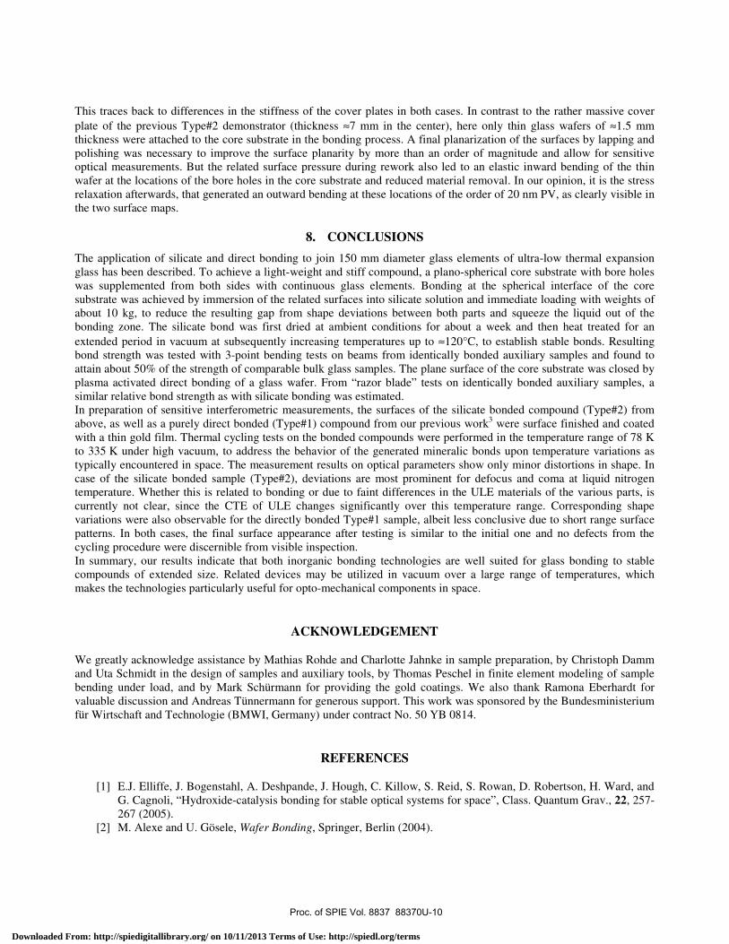
The application of silicate and direct bonding to join 150 mm diameter glass elements of ultra-low thermal expansion glass has been described. To achieve a light-weight and stiff compound, a plano-spherical core substrate with bore holes was supplemented from both sides with continuous glass elements. Bonding at the spherical interface of the core substrate was achieved by immersion of the related surfaces into silicate solution and immediate loading with weights of about 10 kg, to reduce the resulting gap from shape deviations between both parts and squeeze the liquid out of the bonding zone. The silicate bond was first dried at ambient conditions for about a week and then heat treated for an extended period in vacuum at subsequently increasing temperatures up to ≈120°C, to establish stable bonds. Resulting bond strength was tested with 3-point bending tests on beams from identically bonded auxiliary samples and found to attain about 50% of the strength of comparable bulk glass samples. The plane surface of the core substrate was closed by plasma activated direct bonding of a glass wafer. From “razor blade” tests on identically bonded auxiliary samples, a similar relative bond strength as with silicate bonding was estimated. In preparation of sensitive interferometric measurements, the surfaces of the silicate bonded compound (Type#2) from above, as well as a purely direct bonded (Type#1) compound from our previous work3 were surface finished and coated with a thin gold film. Thermal cycling tests on the bonded compounds were performed in the temperature range of 78 K to 335 K under high vacuum, to address the behavior of the generated mineralic bonds upon temperature variations as typically encountered in space. The measurement results on optical parameters show only minor distortions in shape. In case of the silicate bonded sample (Type#2), deviations are most prominent for defocus and coma at liquid nitrogen temperature. Whether this is related to bonding or due to faint differences in the ULE materials of the various parts, is currently not clear, since the CTE of ULE changes significantly over this temperature range. Corresponding shape variations were also observable for the directly bonded Type#1 sample, albeit less conclusive due to short range surface patterns. In both cases, the final surface appearance after testing is similar to the initial one and no defects from the cycling procedure were discernible from visible inspection. In summary, our results indicate that both inorganic bonding technologies are well suited for glass bonding to stable compounds of extended size. Related devices may be utilized in vacuum over a large range of temperatures, which makes the technologies particularly useful for opto-mechanical components in space.
ACKNOWLEDGEMENT
We greatly acknowledge assistance by Mathias Rohde and Charlotte Jahnke in sample preparation, by Christoph Damm and Uta Schmidt in the design of samples and auxiliary tools, by Thomas Peschel in finite element modeling of sample bending under load, and by Mark Schürmann for providing the gold coatings. We also thank Ramona Eberhardt for valuable discussion and Andreas Tünnermann for generous support. This work was sponsored by the Bundesministerium für Wirtschaft and Technologie (BMWI, Germany) under contract No. 50 YB 0814.
REFERENCES
[1] E.J. Elliffe, J. Bogenstahl, A. Deshpande, J. Hough, C. Killow, S. Reid, S. Rowan, D. Robertson, H. Ward, and G. Cagnoli, “Hydroxide-catalysis bonding for stable optical systems for space”, Class. Quantum Grav., 22, 257-267 (2005).
[2] M. Alexe and U. Gösele, Wafer Bonding, Springer, Berlin (2004).
Proc. of SPIE Vol. 8837 88370U-10
Downloaded From: http://spiedigitallibrary.org/ on 10/11/2013 Terms of Use: http://spiedl.org/terms
[3] G. Kalkowski, S. Risse, C. Rothhardt, M. Rohde, and R. Eberhardt, “Optical contacting of low-expansion materials”, Proc. SPIE, Vol. 8126, 81261F3-F7 (2011).
[4] G. Kalkowski, U. Zeitner, T. Benkenstein, J. Fuchs, C. Rothhardt, R. Eberhardt, “Direct wafer bonding for encapsulation of fused silica optical gratings”, Microelectronic Engineering, 97, 177-180 (2012).
[5] H.J. Quenzer, W. Benecke, “Low temperature wafer bonding”, Sens. Actuators A, 32, 340-344 (1992); see also US patent No. 5407865 (1995).
[6] Dz-Hung Gwo, “Ultra-precision bonding for cryogenic fused silica optics”, Proc. SPIE, Vol. 3435, 136-142 (1998); see also US Patent No. 6,548,176 (1998).
[7] S. Rowan, S.M. Twyford, J. Hough, “The design of low loss suspensions for advanced gravitational wave detectors”, in E. Coccia, G. Veneziano, and G. Pizzella, eds., Conference on Gravitational Waves, CERN, Switzerland, 1-4 July, 1997, E. Amaldi Foundation Series, 4, 363–369, (World Scientific, Singapore; NJ, 1998).
[8] M. Krauss et al., US patent application No. 2010/0288422A1 (2010). [9] J. F. Stebbins, Z. Xu, “NMR evidence for excess non-bridging oxygen in an alumino-silicate glass”, Nature,
390, 60-62 (1997). [10] http://en.wikipedia.org/wiki/RCA_clean [11] D. R. Askeland, P. P. Phulé, Science and engineering of materials, Cengage Learning, Stanford (2006). [12] G. Kalkowski, C. Rothhardt, P.-J. Jobst, M. Schürmann, and R. Eberhardt,“Glass Direct Bonding for Optical
Applications”, ECS transactions, Vol. 50, 399-405 (2012). [13] S.H. Christiansen, R. Singh, and U. Gösele,“Wafer Direct Bonding: From Advanced Substrate Engineering to
Future Applications in Micro/Nanoelectronics”, Proc. IEEE, Vol. 94, 2060-2106 (2006). [14] W.P. Maszara, G. Goetz, A. Caviglia, and J.B. McKitterick, “Bonding of silicon wafers for silicon-on-
insulator”, J. Appl. Phys., 64, 4943-4950 (1988). [15] Ö. Vallin, K. Jonsson, U. Lindberg, “Adhesion quantification methods for wafer bonding”, Mater. Sci. Eng. R,
50, 486–495, (2005). [16] P. R. Yoder, Opto-mechanical systems design, CRC Press 2nd ed., New York (1992).
Proc. of SPIE Vol. 8837 88370U-11
Downloaded From: http://spiedigitallibrary.org/ on 10/11/2013 Terms of Use: http://spiedl.org/terms