Embed Size (px)
Citation preview
Silica-based Post-Wall Waveguide with
High-Performance Input and Output Transitions
for E-band Passive Front-end
Yusuke Uemichi(1)
, Osamu Nukaga(1)
, Kei Nakamura(1)
, Xu Han(1)
, Ryouhei Hosono(1)
, and Ning Guan(1)
(1) Fujikura Ltd.
Advanced Technology Laboratory
1440, Mutsuzaki, Sakura-shi, Chiba, Japan
Abstract— We proposed silica-based post-wall waveguides
(PWWs) with input and output (I/O) transitions from microstrip
line for 71-76 GHz and 81-86 GHz, respectively. The PWWs were
designed so that their reflection keeps lower than -20 dB at the
aimed frequencies. They were fabricated in silica substrates and
the performance was measured. Realization of the bandwidth of
23.6% was confirmed at the lower band. The transmission loss of
the sole PWW was 0.0326 dB/mm and the insertion loss of the
transition was 0.25 dB, both at 85 GHz. The silica-based PWWs
can offer a practical platform for passive front-end including
antenna feeds in E-band.
Keywords—Post-wall waveguide, transformer, millimeter-
wave devices, millimeter-wave communication, E-band, antenna
feeds.
I. INTRODUCTION
Millimeter-wave applications such as data communication and sensing use high-frequency band such as E-band (71 GHz-86 GHz), and realization of passive front-end including antenna feeding network for these applications is required. Post-wall waveguide (PWW) has been gaining much attention because it is a promising candidate to realize practical and high-performance millimeter-wave passive devices [1]-[3]. Passive integrations using PWW based on low-temperature co-fired ceramics (LTCC) have been researched intensively [4]-[6].
On the other hand, microstrip line (MSL) is a typical transmission line of millimeter-wave CMOS-IC [7]. Therefore, a transition between PWW and MSL is required for connection between PWW based passive front-end and CMOS-IC. In [6], input and output (I/O) transitions between MSL and PWW for V- and W-band are reported. But the design and structure are complicated because of matching components and multi-layered structure. Reflection loss also needs to be improved.
To provide low-loss PWW that can easily be integrated with E-band RFICs, we have realized PWW with I/O transitions between MSL and PWW in silica substrate. In this paper, the geometry of our PWW with I/O transitions is firstly explained. Then, the design of the E-band I/O transition is
discussed and compared with that for 60-GHz band. Finally, measurement results and discussions on losses are presented.
II. GEOMETRY AND DESIGN
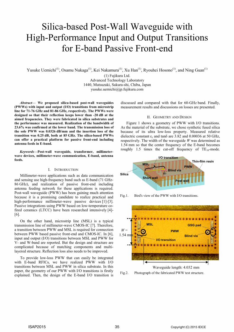
Figure 1 shows a geometry of PWW with I/O transitions. As the material of the substrate, we chose synthetic fused silica because of its ultra low-loss property. Measured relative
dielectric constant r and tan are 3.82 and 0.00036 at 50 GHz, respectively. The width of the waveguide W was determined as 1.54 mm so that the center frequency of the E-band becomes roughly 1.5 times the cut-off frequency of TE10-mode.
Fig.1. Bird's view of the PWW with I/O transitions.
MSL
Blind via
Post wall
Silica Short wall
PWW
Fig.2. Photograph of the fabricated PWW test structure.
MSL
Waveguide length: 4.032 mm
PWW
I/O transition
GSG pad
W =
1.54 mm Blind via
I/O transition
Thin-film resin
ISAP2015 Copyright (C) 2015 IEICE35

Diameter of the post and the spacing among them are 100 m
and 200 m, respectively. The waveguide thickness is 0.52 mm. On the PWW, thin-film resin is formed to realize MSL. The
width of the MSL is set to 55 m to realize 50 - characteristic impedance. The MSL is connected to a blind via inserted into PWW, which plays a role to excite TE10-mode from quasi TEM-mode in the MSL. Figure 2 shows the fabricated PWW test structure (two back-to-back transitions connected by PWW) designed for the 71-76 GHz band. In our silica-based technology, the depth of the blind via can be realized at an arbitrary value, which differs greatly from the situation of conventional multi-layered LTCC technology [6]. Figure 3 shows a cross-sectional side view of the I/O transition with design parameters. The dielectric thickness of the MSL q is
20 m. The anti-pad space s and land-size p are 60 m and
50 m, respectively. The opening-diameter of the dielectric D
is 150 m. L is the distance between the short wall and the blind-via, which is set to a value approximately between 16 and 18% of the guided wavelength at the aimed frequency. Figure 4(a) shows the simulated |S11| for several blind-via
depths h when L is 484 m, where L of 484 m is 16.5% of the guided wavelength at 73.6 GHz in the 71-76 GHz-band. The simulated results were obtained by using the 3D-electromagnetic simulation software HFSS. In the simulation model, port 1 is set at the end of the MSL and port 2 is set at the edge of the PWW as shown in Fig. 3. We can see the
reflection gets smallest when h is 460 m. Figure 4(b) shows the simulated |S11| for several blind-via depths h when L is
575 m for comparison, where L of 575 m is 16.5% of the guided wavelength at 60 GHz. The width of the waveguide in the simulation-model is determined as 2.0 mm in the same manner as the design for 71-76 GHz band. We can see the
reflection gets smallest when h is 490 m. We can infer from these results that the depth of the blind via h required for E-band applications is smaller than that required for 60-GHz applications if the thickness of the waveguide is common. In
the design for the 81-86 GHz-band, L is determined as 410 m which is 17.5% of the guided wavelength at 83.6 GHz
The fabrication processing is done as follows. Firstly we irradiate high-power laser beam to places in a silica substrate where holes for the blind-vias and posts are to be opened by scanning a femtosecond laser. The irradiation will locally reform the material of the substrate. Secondly the reformed substrate is etched by hydrofluoric acid solution, where the irradiated portion of the substrate is selectively etched. Finally, the blind vias and posts are metallized by sputtering and Cu-electroplating. In this way, we can realize ideal blind vias for the optimized design. In the actual fabrication, h is targeted as
450 m for both of the 71-76 GHz band design and 81-86 GHz one.
III. MEASURED RESULTS
We measured the PWW test structure shown in Fig.2 using a 90-GHz network analyzer. The test structures were prepared separately for the 71-76 GHz band and the 81-86 GHz one.
Firstly, reference plane was moved to the 150 m-pitch probe tip through LRM calibration. Then we measured all the structures including two I/O transitions. The length of the
waveguide is 4.032 mm. Figure 5 shows the measured and simulated results of the test structure designed for the 71-76 GHz band, where the measured results are not deembedded. |S11| is less than -20 dB between 66.4 GHz and 84.2 GHz, and is less than -15 dB at the frequencies higher than 65 GHz. So it has more than 32.2% bandwidth and covers the aimed 71-76 GHz band sufficiently. |S21| at 75 GHz is 0.52 dB. One of the causes for the discrepancy between the simulation and measurement above 75 GHz might be the effects of the pads for probing. There is also possibility of the intrinsic material property above 75 GHz being slightly different from what was specified at 50 GHz.
Figure 6 shows the measured and simulated results of the test structure designed for the 81-86 GHz band, where the waveguide length is 4.18 mm and the measured results are not
Fig.3. Cross-sectional side view of the I/O transition with design-parameters.
(a)
(b)
Fig.4. Simulated |S11| for several depths of blind via h at the frequencies of (a) 60-80 GHz and (b) 50-70 GHz, respectively.
100m
h pl
d
q sl
Port2
Ll
MSL
Dl
Port1
Short wall
Blind via 0.52 mm
W = 1.54 mm
L = 484 m
W = 2.00 mm
L = 575 m
36

deembedded either. |S11| is less than -20 dB at the frequencies higher than 77.7 GHz and is less than -15 dB at those higher than 75 GHz. So it has more than 18% bandwidth and covers the aimed 81-86 GHz band sufficiently. |S21| at 85 GHz is 0.61 dB, which is slightly higher than one at 75 GHz. In both of the design for the 71-76 GHz band and that for 81-86 GHz one, we could realize much better reflection loss than the reported work using multi-layered structure of LTCC [6].
We also fabricated test structures with the waveguide lengths of 9.03 mm and 19.03 mm. Figure 7 shows |S21| versus length at 85 GHz under a condition of |S11| being less than - 15 dB. The slope of the dotted line indicates the transmission loss per unit length, by which the loss of the fabricated PWW at 85 GHz is estimated to be 0.0326 dB/mm. The y intercept of –0.497 dB means the loss originating from all the structures except PWW, such as two I/O transitions, MSLs and pads for probing. The insertion loss of one I/O transition is estimated to be half of the 0.497 dB, i.e., 0.25 dB at 85 GHz.
IV. CONCLUSION
In this paper, we demonstrated silica-based low-loss post-wall waveguide (PWW) with broadband input and output transitions between microstrip line and PWW for E-band
application. 50 -input impedance matching was accomplished by designning a unique blind via without using any matching components and multi-layered structure. The bandwidth is the widest among those ever reported, to our knowledge. The insertion loss of the transition was as small as 0.25 dB at 85 GHz. We also compared the design of the transition between the aimed E-band and 60-GHz band and showed the required depth of the blind via in the transition for the E-band is smaller than that for the 60-GHz band through the simulation and the experiment for the first time.
REFERENCES
[1] Y. Li and K. -M. Luk, “A low-cost high gain substrate integrated waveguide fed patch antenna array for 60-GHz applications,” in Proc. Asia-Pacific Microw. Conf., pp. 459-461, Nov. 2014.
[2] J. Xu, Z. N. Chen and W. Hong, “Bandwidth enhancement for a 60 GHz substrate integrated waveguide fed cavity array antenna on LTCC,” IEEE Trans. Antennas Propag., vol. 59, no. 3, pp. 826-832, Mar. 2011.
[3] A. García-Lampérez, M. Salazar-Palma and S. H. Yeung, “SIW compact diplexer,” in IEEE MTT-S Int. Microw. Symp. Dig., pp. 1-4. Jun. 2014.
[4] X. Wang and A. Stelzer, "A 79-GHz LTCC RF-frontend for short-range applications," IEEE MTT-S Int. Microwave Symp. Dig., pp. 1-4, Jun. 2011.
[5] F. Bauer, X. Wang, W. Menzel and A. Stelzer, “A 79-GHz rader sensor in LTCC technology using grid array antennas,”IEEE Trans. Microw. Theory Techn., vol. 61, no. 6, pp. 2514-2521, Jun. 2013.
[6] I. Ocket, W. De Raedt and B. Nauwelaers, "Microstrip to buried waveguide probe feeds for V- and W-band in LTCC technology," IEEE MTT-S Int. Microwave Symp. Dig., pp. 1-4, Jun. 2013.
[7] Y. Tsukui, H. Asada, C. Han, K. Okada and A. Matsuzawa, " Area Reduction of Millimeter-Wave CMOS Amplifier Using Narrow Transmission Line," in Proc. Asia-Pacific Microw. Conf., pp. 797-800, Dec. 2011.
Fig.7. Relationship between the measured |S21| at 85 GHz and waveguide length
Fig.5. Measured (solid lines) and simulated (dashed lines) S-parameters of the test structure designed for the 71-76 GHz band.
band.
|S21| (dB) = -0.0326Lwg-0.497
Fig.6. Measured (solid lines) and simulated (dashed lines) S-parameters of the test structure designed for the 81-86 GHz band.
37


![Dispersion-Compensation Technique for Log …ap-s.ei.tuat.ac.jp/isapx/2011/pdf/[FrA4-4] A06_1002.pdfDispersion-Compensation Technique for Log-Periodic Antennas using C-section All-Pass](https://img.dokumen.tips/doc/110x75/5fe2247ddedfd0279f38caa6/dispersion-compensation-technique-for-log-ap-seituatacjpisapx2011pdffra4-4.jpg)


