Embed Size (px)
Citation preview

1
DesignCon 2007
Signal Integrity Analysis for
Inductively Coupled Connectors
and Sockets
Karthik Chandrasekar, NC State University
John Wilson, NC State University
Evan Erickson, NC State University
Zhiping Feng, NC State University
Jian Xu, NC State University
Stephen Mick, NC State University
Paul Franzon, NC State University

2
Abstract We demonstrate multi-Gbps pulse signaling with inductively coupled interconnects
across printed circuit boards and packaging interfaces. This has application in realizing
sub-mm pitch Zero Insertion Force (ZIF) surface mount connectors and sockets. The
signaling data rate achievable in our system is from 1Gbps to 8.5Gbps, which depends on
the 3dB coupling frequency of the composite channel consisting of the inductive
interconnections and the transmission lines. Methods to improve signal integrity in
inductively coupled systems are established. Options include transformer geometry
optimization, integrated series terminations and system level tradeoffs.
Author(s) Biography
Karthik Chandrasekar received his Bachelor’s degree in Electrical and Electronics
Engineering in SVCE, Chennai in May 2000. He received his MS degree in Computer
engineering at NCSU in August 2002. He started the PhD program at NCSU in August
2002 and is finishing up dissertation writing on a part-time basis expecting to Graduate in
Feb’ 07. He spent summer of 2005 interning at Nvidia, Santa Clara in the Substrate
system design group and he joined as a full-time employee in October 2006. In the long
term he is interested in a career in areas spanning signal integrity, package layout &
modeling, RF IC design and custom circuit design for high speed serial links.
John M. Wilson received the B.S., M.S., and Ph.D.degrees in electrical engineering from
North Carolina State University (NCSU), Raleigh, in 1993, 1995,and 2003, respectively.
His Ph.D. research focused on the design of RF MEMS tunable capacitors.In 1996, he
was with IBM designing analog circuits for networking ICs, and in 2000, he was with a
start-up company designing circuits for RFID tags. Currently, as a Research Assistant
Professor at NCSU, he is leading a research effort on AC-coupled interconnect and 3D-
ICs.
Evan Erickson received the B.S. and M.S. degrees in computer engineering from North
Carolina State University (NCSU), Raleigh, in 2001 and 2002 respectively. He is
currently working towards his Ph.D. degree in electrical engineering at NCSU. His
research interests include inductor and transformer modeling, high speed chip-to-chip
communication, and high speed equalization schemes.
Zhiping Feng received the B.S. degree in physics from Beijing University, Beijing,
China, in 1987, the M.S. degree in physics from Bowling Green State University,
Bowling Green, OH, in 1994, and the Ph.D. degree in electrical engineering at the
University of Colorado at Boulder in 1999.She is a post-doc in Department of Electrical
and Computer Engineering, NCSU. Prior to join NCSU, she was a Sr. Staff Engineer in
ComSpace Co. Coppell, TX. Her research interests include RF/Microwave applications
3
of BST and MEMS. She is also interested in RF modeling of flip-chip and AC coupled
interconnects and 3-D packaging.
Jian Xu received the B.S. degree in electrical engineering at Huazhong University of
Science and Technology, China, in 1993. He is currently pursuing the Ph.D. degree in
electrical and computer engineering at North Carolina State University, Raleigh. He did
summer internships at Motorola Laboratories and the IBM T.J.Watson Research Center
in 2002and 2005, respectively. His research interests include high-speed chip-to-chip
communications, vertical signaling in 3D-IC and chip-package co-design.
Stephen E.Mick received the B.S. degree in electrical engineering from the University of
Houston, Houston, TX, in 1995, and the M.S. and Ph.D. degrees in electrical engineering
from North Carolina State University, Raleigh, in 1998 and 2004, respectively. While
studying for the B.S.E.E. degree and after graduation, he worked at Texas Instruments,
Dallas, TX, as an Applications Engineer, ASIC Designer, and Program Manager. His
research interests include developing I/O techniques and interfaces for high-speed chip-
to-chip communications and both micro- and nano-fabrication technologies.
Paul D. Franzon (SM’99–F’06) received the Ph.D. degree from the University of
Adelaide, Adelaide, Australia, in 1988.He is currently a Distinguished Alumni Professor
of Electrical and Computer Engineering at North Carolina State University, Raleigh. He
was with AT&T Bell Laboratories, DSTO Australia, Australia Telecom, and two
companies he cofounded, Communica and LightSpin Technologies. His current interests
center on the technology and design of complex systems incorporating VLSI, MEMS,
advanced packaging and molecular electronics. Application areas currently being
explored include novel advanced packaging structures, Network Processors,SOI
baseband radio circuit design for deep space, on-chip inductor and inductance issues, RF
MEMS, and moleware circuits and characterization. He has lead several major efforts and
published over 120 papers in these areas. Dr. Franzon received an NSF Young
Investigators Award in 1993, in 2001was selected to join the NCSU Academy of
Outstanding Teachers, and in 2003was selected as a Distinguished Alumni Professor.

4
1. Introduction
Inductively coupled interconnects have shown potential for multi-Gbps signaling in chip
to chip communication and 3D IC’s [6, 7]. Inductively coupled interfaces can be used in
level 3 interconnections (board-board connectors) [2] and level 2 interconnections
(package-board interconnections) as well. Insertion force and mechanical stress in high
pin count mechanically mated interconnections can be addressed by using contactless
inductively coupled elements for high speed signal connections while using fuzz buttons
[5], for power, ground connections and to provide a rigid mechanical interface . Surface
mount backplane connectors offer electrical advantages over conventional press-fit style
designs, but they suffer from coplanarity issues and their commercial deployment is
sparse [1]. The objective of this work is to demonstrate potential for a viable sub-mm
pitch “ZIF” surface mount connector technology using inductive elements. Figure 1
shows a high level depiction of the end goal of our work.
Figure 1: Inductively Coupled Connector Interface
Section 2 discusses signaling choice for inductive connectors, section 3 discusses
performance needs for connectors, section 4 discusses transformer modeling and
optimization to achieve good signal integrity, section 5 discusses experimental work and
section 6 discusses future potential.
2. Signaling Options for an Inductive Connector System
Transformers can be used in theory for non return to zero (NRZ) or pulse signaling. Step
response is illustrated for the two cases in Figure 2. The input signal in our system is
broadband digital NRZ data; output waveform from the transformer can be faithfully
reproduced NRZ or pulses depending on the value of inductances. An ideal transformer is
a high pass filter and the value of inductance sets the 3dB high pass coupling frequency
for the filter. NRZ signaling with a transformer in a 50 ohm system needs fairly large
values of inductances to be able to couple data across a wide band of frequencies from
close to DC to the knee frequency corresponding to the digital edge. As shown in Figure
3, when inductance values approach 500nH there is minimal low frequency attenuation in
the forward power transfer (S21) and this would lead to faithful reproduction of the input

5
NRZ waveform. However it is impractical to realize 500nH inductance values in
available board level processes in sub-mm pitch footprints. For e.g. the maximum
inductance realizable in a process with 25um trace width/space and 75um microvias in a
775um outer diameter is 22nH.
Figure 2: NRZ and Pulse signaling across a transformer
Figure 3: Frequency response for ideal transformer in Figure 2
More realistic option for sub-mm pitch inductive connector system is pulse signaling. All
the information in a digital signal is in the high frequency content of the edge. This
information can be used to detect a 1 to 0 and 0 to 1 transition. A transformer realized
with small inductance values ranging from 1nH~5nH can be used to read high frequency
information in the edge while attenuating low frequency components. This can be used to
convert input step to pulses as shown in Figure 2. These pulse waveforms can then be
recovered back to NRZ through circuit techniques [7, 9].
6
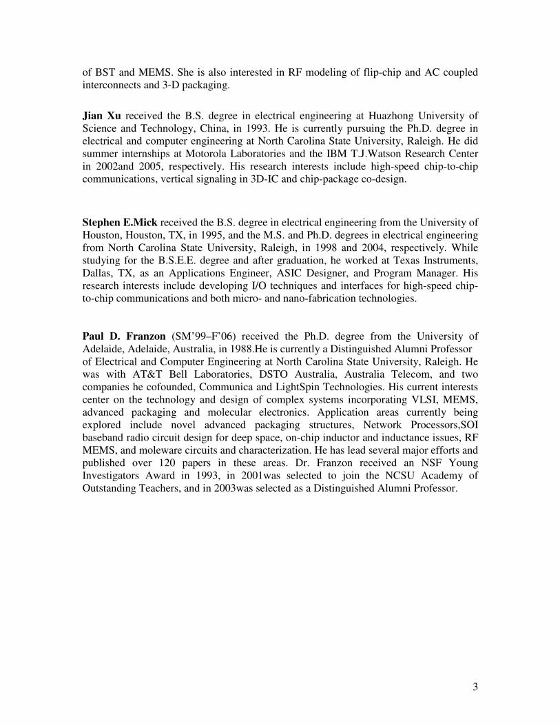
3. Electrical Performance Requirements for a Connector/Socket
In simplistic terms the goal of a good connector is to achieve maximum forward signal
transfer with minimal reflections from discontinuities. The goal of the transformer used
as a connector is to achieve optimal values of insertion loss (S21) and return loss (S11).
Figure 4: Inductive connector performance metrics
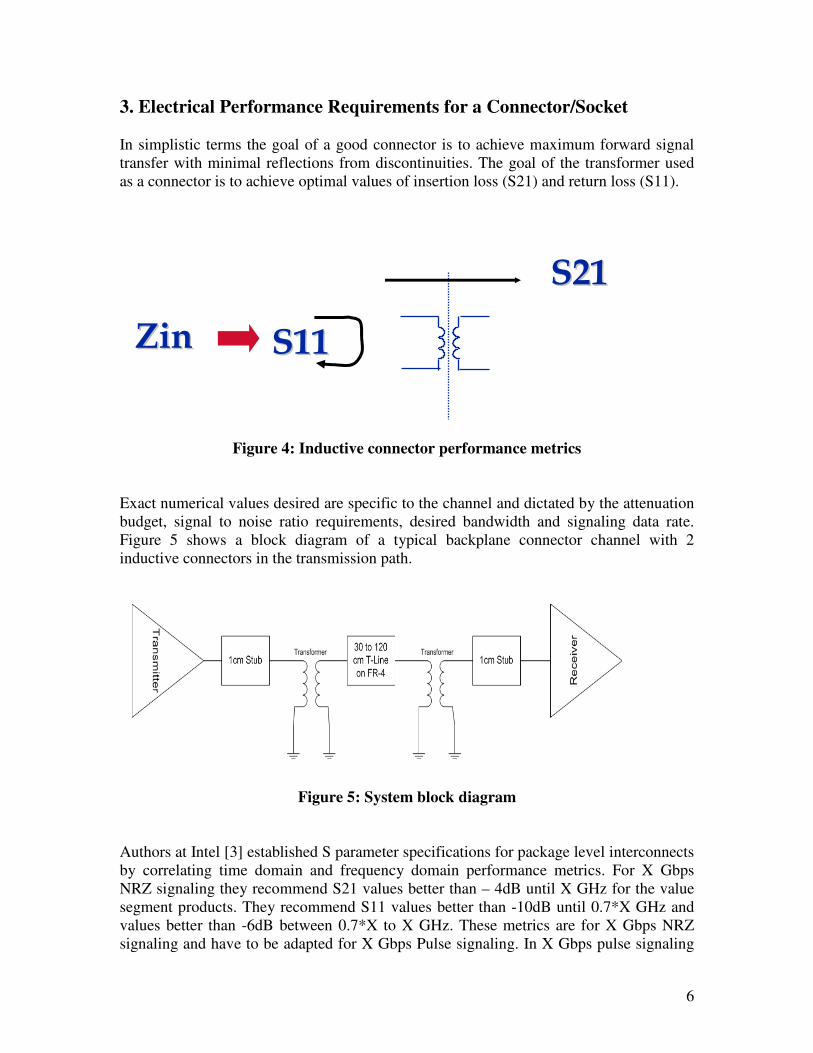
Exact numerical values desired are specific to the channel and dictated by the attenuation
budget, signal to noise ratio requirements, desired bandwidth and signaling data rate.
Figure 5 shows a block diagram of a typical backplane connector channel with 2
inductive connectors in the transmission path.
Figure 5: System block diagram
Authors at Intel [3] established S parameter specifications for package level interconnects
by correlating time domain and frequency domain performance metrics. For X Gbps
NRZ signaling they recommend S21 values better than – 4dB until X GHz for the value
segment products. They recommend S11 values better than -10dB until 0.7*X GHz and
values better than -6dB between 0.7*X to X GHz. These metrics are for X Gbps NRZ
signaling and have to be adapted for X Gbps Pulse signaling. In X Gbps pulse signaling
SS2211
SS1111 ZZiinn

7
the goal is to achieve sufficient S21 with acceptable signal to noise ratio for recovery to
NRZ by the Receiver section shown in block diagram in Figure 5. Custom pulse receiver
circuits as discussed in [7, 9] have to be used. A typical requirement for a pulse receiver
circuit is 200mV peak to peak input signal with SNR ratio better than 20dB for recovery
to NRZ.
4. Transformer Modeling and Optimization
4.1 Transformer Model
Figure 6: Transformer Geometry and Equivalent circuit
High fidelity transformer models are important to predict performance before building
them. The elements in the model depend on the geometry of the inductor coils, the
substrate they are realized on and return paths. Figure 6 shows the baseline model
adopted in this work which correlates with transformer physical geometry. Here L
represents the inductance of the primary and secondary coils assuming they are equal. K
represents the magnetic coupling coefficient between the coils. Cc is the crossover
capacitance arising due to the overlap area of the two coils. Cp is the parasitic
capacitance to ground for the coils. R is the winding resistance for the coils. The model
can be expanded to distributed structures by cascading multiple sections of the lumped
model. EM tools like Sonnet or HFSS can be used for modeling distributed structures.
The choice of whether to use a lumped model or a distributed model must be made based
on the electrical length of the structure. For example the edge rate in most high speed
digital applications is ~70ps. This sets the knee frequency at 7GHz. If the electrical
length of a structure is less than or equal to one tenth of operating wavelength at 7 GHz
then a lumped model would suffice, else distributed or EM modeling is needed. The
model in Figure 6 ignores skin effect. Skin effect should be modeled for thicker
metallization while it can be ignored for thinner metallization. This work focuses on

8
inductors realized on laminate and packaging substrates as opposed to conductive silicon.
Hence some of the complexity associated with modeling capacitive parasitics associated
with a conductive substrate is eliminated. We focus on optimizing values of inductance,
magnetic coupling coefficient, winding resistance and crossover capacitance.
4.2 Transformer Model Parameter Optimization
4.2.1 Choice of Inductance Values
The choice of inductance values is a tradeoff between signal amplitude and signaling data
rate. Figure 7 shows simulation setup for an ideal transformer with 1V peak input with
100ps edge rate. Figure 8 shows a plot of the pulse waveforms at the output of the
transformer for different values of L1 and L2. The data is summarized in Table 1. For
example a transformer realized with 5nH inductors takes 0.561nsec to decay down to
10% of it’s peak voltage. If we can tolerate 10% of inter-symbol interference between
adjacently transmitted data bits, this implies a 1.78Gbps peak signaling data rate. Faster
decay times are achieved with 1nH inductors with the tradeoff being reduced signal
swing. The attenuation budget of the end system the connector is deployed in will
determine the engineering tradeoff in choosing appropriate values of inductance.
Figure 7: Simulation setup to study inductance value tradeoffs

9
Figure 8: Step response for different values of L1, L2 in Figure 7
L1 = L2 = L(nH) Settling time to 10%
of peak voltage (nsec)
Peak Voltage (mV)
1nH 0.190 nsec 183.5mV
5nH 0.561 nsec 393.5mV
15nH 1.5 nsec 460mV
25nH 2.45 nsec 475mV
Table 1: Tradeoff between data rate and signal amplitude
The decay rate of the inductive elements can be impacted beneficially by high impedance
load terminations to increase the signaling data rate. However the output of inductive
connectors or sockets is loaded by a 50 ohm transmission line on package or FR4. The
choice of 50 ohms characteristic impedance for the traces is driven by routing density and
optimum performance characteristics on FR4/package. Hence it is hard to impact system
performance beneficially by varying load terminations. If differential signaling were
employed in the connector with two identical 50 ohm lines the differential impedance
looking in is 100 ohms. The decay rate for the coupled inductors would be faster for
coupled inductors in a 100 ohm system compared to a 50 ohm system. This could have
some application in achieving faster speeds with differential connectors as opposed to
single ended connectors.
4.2.2 Magnetic Coupling Coefficient (K<1)
High magnetic coupling coefficient values are desirable in inductively coupled
connectors for improving insertion loss and return loss, and increasing bandwidth. Figure

10
9 shows the T circuit model for a transformer with K<1. As the K reduces the value of
the leakage inductances in the model L1-M & L2-M grow which in turn contribute to
high frequency roll off in forward transfer function, more loss and also impedance
mismatches.
Leakage inductance
Figure 9 : T-circuit model for a transformer with leakage (M=K√L1L2)
Figure 10 shows a simple transformer model assumed for the discussion in this section.
Mutual
Mutual1
K=
MUTIND
Port
P2
Num=2
Port
P1
Num=1
Term
Term2
Z=50 Ohm
Num=2
Term
Term1
Z=50 Ohm
Num=1 L
L2
L=5 nH
L
L1
L=5 nH
Figure 10: Transformer model to analyze variation of K
Figure 11 shows how S21 changes as the leakage inductance increases when K drops
from 1 to 0.6.

11
Figure 11 : S21 for increasing leakage inductance (assuming L1=L2=5nH)
As K drops the 3dB bandwidth of the system reduces and the loss through the system also
increases. For example when K changes from 0.8 to 0.6 the 3dB bandwidth of the system
reduces from 8.9 GHz to 4.9 GHz. Figure 12 shows S11 for increasing leakage
inductance.
Figure 12 : S11 for increasing leakage inductance ( L1=L2=5nH)
When K=1 the S11 is better than -10dB 2GHz onwards. A deviation of K from 1 to 0.8
degrades the return loss values to less than -5dB. The magnetic coupling coefficient
between two vertically stacked planar spiral inductors is a function of many factors, such
as: gap spacing, inductance and effective area. In a level 2 or level 3 interconnect
application, the achievable gap spacing between the coupling elements is limited by the
surface roughness of FR4, and the thickness of the interlayer dielectric used to isolate the
coupling elements. The surface roughness of FR4 can range from 1µm to 10µm [10],
which produces a large and unpredictable variation in the gap spacing. Figure 13 shows
K vs gap spacing(d) extracted using ASITIC for a sample transformer structure. The

12
transformer chosen is 500um in outer diameter with 25um trace width/space and 3 turns.
The extracted value of inductance is 5.13nH.
Figure 13 : K vs Gap spacing(d) extracted using ASITIC for a 500um diameter
transformer
4.2.3 Broadband impedance matching
In Figure 13, the value of K is 0.67 when gap spacing is 25um which is a reasonable
value to expect in board to board stacked setup. This would produce unacceptable values
of return loss and cause high frequency roll off in S21 based on our analysis in Figures
11, 12. This can be compensated for by using inherent crossover capacitance part of the
transformer coil to tune the return loss and insertion loss at high frequencies. Controlling
the low frequency return loss needs lossy elements like a series resistance since
electrically a transformer is a short-circuit at DC. Figure 14 shows an electrical model
for a transformer which can achieve broadband matching as shown in Figure 15. It is
feasible to realize the model parameters shown in Figure 14 through simple transformer
geometrical variations. Realizing 25 ohms series resistance on laminates/packages would
require ability to fabricate thin metallization on packages or integrated buried resistors.
0
0.2
0.4
0.6
0.8
1
1.2
0 10 20 30 40 50 60 70 80 90
Gap Spacing ( in Microns)
Coupling C
oeff
icie
nt (K
)
Series1

13
Figure 14: Optimal Transformer Model
Figure 15: Frequency response
Optimal values of R, Cc to achieve broadband impedance matching for a given value of
L, K can be determined from ABCD matrix computations on simple lumped model
approximations for transformers. A point to be noted is that excess crossover capacitance
can negatively impact transformer step response due to overshoots and oscillations. So
the value of crossover capacitance chosen to tune the frequency response should be as
small as possible [8]. The transformer model parameters shown in Figure 14 can be
realized in small electrical winding lengths. This makes it feasible to predict performance
accurately with simple lumped models.
14
5. Experimental work – Inductive Connector Prototypes
5.1 Proof of Concept
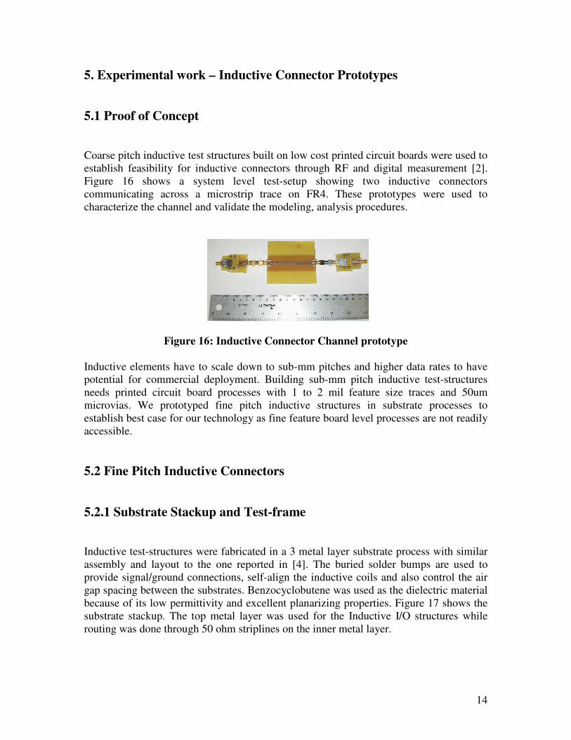
Coarse pitch inductive test structures built on low cost printed circuit boards were used to
establish feasibility for inductive connectors through RF and digital measurement [2].
Figure 16 shows a system level test-setup showing two inductive connectors
communicating across a microstrip trace on FR4. These prototypes were used to
characterize the channel and validate the modeling, analysis procedures.
Figure 16: Inductive Connector Channel prototype
Inductive elements have to scale down to sub-mm pitches and higher data rates to have
potential for commercial deployment. Building sub-mm pitch inductive test-structures
needs printed circuit board processes with 1 to 2 mil feature size traces and 50um
microvias. We prototyped fine pitch inductive structures in substrate processes to
establish best case for our technology as fine feature board level processes are not readily
accessible.
5.2 Fine Pitch Inductive Connectors
5.2.1 Substrate Stackup and Test-frame
Inductive test-structures were fabricated in a 3 metal layer substrate process with similar
assembly and layout to the one reported in [4]. The buried solder bumps are used to
provide signal/ground connections, self-align the inductive coils and also control the air
gap spacing between the substrates. Benzocyclobutene was used as the dielectric material
because of its low permittivity and excellent planarizing properties. Figure 17 shows the
substrate stackup. The top metal layer was used for the Inductive I/O structures while
routing was done through 50 ohm striplines on the inner metal layer.

15
Figure 17: 3 layer substrate process with buried bumps (2um thick copper
metallization & BCB dielectric with Er=2.65)
One of the substrates was flipped onto its corresponding mating sample with buried
bumps to create the test interface for characterizing inductive coupling. Figure 18(a)
shows a cross sectional view of the test-setup and Figure 18(b) shows a sample photo of
an inductor on the bottom substrate.
18(a) Cross-sectional view 18(b) Photo of Inductor on substrate
Figure 18: Test Frame for characterizing inductive coupling
The air gap spacing between the inductors on the substrates is estimated to be 5~8um
based on best case and worst case capacitor measurements which were made across the
interface.
5.2.2 Transformer Characterization
Transformers of various outer diameters with geometrical variations on trace width/space
were built on the substrate. Inductance values were optimized to achieve 2Gbps+
signaling speeds with sufficient signal swing. Transformer geometrical variations were
designed to achieve K>=0.6 across 5~8um air gaps with minimal parasitics. A tradeoff
was made between inductance values and K to keep the leakage inductance under control
as well. The shunt capacitive parasitics for the transformer structures were minimized by
keeping ground returns away by a certain fraction of the outer diameter. Figure 19 shows
S21 and S11 measurements for a 100um diameter transformer SB1_11a.

16
Figure 19: Measured data for a 100um diameter transformer (SB1_11a) (with
1.22nH inductors realized with 5um trace width/space) across a gap spacing of
5~8um.
Figures 20(a) and 20(b) shows the measured eye diagram for transformer SB1_11a for
27-1 PBRS data at 4.25 Gb/sec and 8.5 Gb/sec with 25ps edge rates. Time domain
measurements were made with an Agilent N4901b serial BERT and a Tek11801A
oscilloscope.
20(a) Eye diagram at 4.25 Gb/sec 20(b) Eye diagram at 8.5 Gb/sec
Figure 20: Measured data for a 100um diameter transformer (SB1_11a) (with
1.22nH inductors realized with 5um trace width/space) across a gap spacing of
5~8um.
Figure 21(a) shows the electrical model for the transformer SB1_11a. Values of magnetic
coupling coefficient (K) and inductance in the model were extracted using ASITIC.
Shunt capacitive parasitics are very small and make minimal impact on the model since
the inductor is on a low loss substrate as opposed to conductive silicon. Also the ground
plane is removed in the area immediately surrounding the inductor to reduce shunt
capacitive parasitics and to prevent eddy currents. The DC Resistance at port 1 was
measured to be 7.5 ohms which correlates closely with 7.6 ohms used in the model.
Figure 21(b) shows the measured vs simulated S21 and S11. Figure 22 shows the
measured vs simulated phase. Lossless transmission line models from ADS were used to
include the effect of the 50 ohm feedlines from the probe pad to the inductor. The lengths
of the feedlines are asymmetric since there are multiple columns of inductor experiments

17
which need to be routed to corresponding probe pads. Note that a simple circuit model
provides a broadband match from 50MHz to 18 GHz for both phase and magnitude
information due to the lumped nature of the transformer. The electrical length of this
structure is 1.1mm and approaches 1/10th
of the operating wavelength at only 17 GHz and
hence lumped models would be valid over decades of bandwidth. This would save a lot
of simulation time which is needed for full wave EM simulations in commercial
connectors.
21(a) Lumped circuit model 21(b) Measured vs Simulated S21, S11 (Mag)
Figure 21: Measured vs simulated results for 100um diameter transformer
(SB1_11a)
Figure 22: Measured vs simulated S21 for SB1_11a (Phase)
Table 2 summarizes measurements on experiments SB1_11a and SB1_11b. We are able
to achieve 8.5 Gb/sec signaling with a 100um diameter transformer which is built with
1.2nH inductances and 2.5 Gb/sec signaling with a 100um diameter transformer built
with 4nH inductances. The 3dB bandwidth is fairly high for these structures and this
could help in scaling to higher data rates in the future. The goal of these substrate
assembly experiments were to determine best case signaling data rate and pitch for
transformer interconnect structures in a process accessible to us.

18
Table 2: Summary of Transformer Measurements SB1_11a, SB1_11b
The return loss characteristics for structures SB1_11a and SB1_11b are poor from
measurement because the crossover capacitance between the two inductor coils in this
measurement is very small. For example the crossover capacitance is estimated to be
9~15fF for structure SB1_11a from simple parallel plate formulae. Since the gap spacing
is fixed by the solder bump height it is hard to vary the crossover capacitance in
measurement. Improving the high frequency return loss for this structure requires a boost
in the cross-over capacitance through increasing trace width, reducing gap spacing or
increasing dielectric constant without degrading step response of the transformer. Low
frequency return loss can be improved through a 20 to 50 ohm integrated series
terminator on board. The tradeoff in achieving the improved return loss with the series
termination is more attenuation. In a system application an inductive connector would be
used to communicate over 10cm to 1m long lines on FR4 and in this case the losses in the
line can be used to dampen out the reflections as well.
Transformer
Sample #
(100um Outer
diameter)
Inductance
(from
ASITIC)
3dB high
pass
coupling
frequency
3dB
bandwidth
AC coupled eye
opening
SB1_11a 1.22nH 3.6 GHz 15.2 GHz 400mV pp @
4.25 Gb/sec
200mV pp @
8.5 Gb/sec
SB1_11b 4.12nH 947 MHz 8.6 GHz 550mV pp @
1.25 Gb/sec
450mV pp
@2.5Gb/sec

19
6. Future Potential
Experimental work in section 5 showed prototype of a fine pitch inductive connector for
signaling speeds upto 8.5Gb/sec. 5um trace width/feaures available in the substrate
process were used to realize 100um diameter transformers with 1.2nH inductance. In a
laminate process with 25um trace width/space and 50um microvias a 1.2nH inductance
can be realized in a 275um diameter structure. Crosstalk constraints would drive the
spacing between adjacent inductors to be 1/5th
of the outer diameter [2]. This implies that
we can build 345um pitch inductive connectors in a laminate technology and these can be
single ended or even differential. Table 3 shows outer diameters required for realizing a
1.2nH inductance when trace width/space varies from 5um/5um to 25um/25um.
Prototype Case (SB1_11a) PCB/Package Process
5um Trace width/Space 25um Trace width/space
Via size : 10um Via size : 50um
100um Outer diameter 275um diameter
1.2 nH inductance 1.15nH inductance
Table 3: Implementation of ~1.2nH inductance with different feature sizes
Figure 23 shows potential implementation for inductive connectors in the future. Fuzz
buttons can be used to provide DC connections and act as a mechanical interface while
inductive elements can be used for high speed contactless signal connections. An area
array of I/O pads on Flex daughter card can mate with corresponding set of signal pads
on the backplane.

20
Figure 23: Backplane connector system with inductive elements
7. Conclusion
Multi Gbps pulse signaling is feasible with sub-mm pitch inductive connectors.
Crossover capacitance tuning, series resistance, leakage inductance control and parasitic
capacitance control can be used to achieve broadband S21 and S11. Return loss tuning is
sensitive to crossover capacitance tuning. Hence well controlled gap spacing between
inductive coils is important for robust performance. Inductive connectors are well suited
in custom applications where the air gap spacing, process feature sizes, edge rate,
attenuation budget and signaling data rate are well known.
Acknowledgements:
This work is supported by AFRL contract F29601-03-3-0135 and by NSF under grant
CCR-0219567. We would like to thank RTI, North Carolina for solder bumping services.
We also thank Yongjin Choi, Ambrish Varma and Steve Lipa at the ECE Department,
NC State for their inputs during technical discussions.

21
References:
1. R. Kollipara and B. Chia, “Modeling and Verification of Backplane Press-Fit PTH
Vias “, DesignCon2004.
2. K. Chandrasekar, Z. Feng, J. Wilson, S. Mick, P. Franzon, “Inductively coupled
board-to-board connectors,” IEEE Electronic components and technology conference
(ECTC), May 2005, pp.1109-1113
3. U.A Shrivastava,V.Prokofiev,Chee Hoo Lee,A.Augustine,L.Polka, “Package Electrical
Specifications for Giga bit Signaling I/Os “, IEEE ECTC 2003, pp.1452-1458
4. J.Wilson, S.Mick, J.Xu , L.Luo, S.Bonafede,A.Huffman,R.Labennett and Paul
Franzon, “Fully Integrated AC Coupled Interconnect using Buried Bumps”, IEEE
Electrical performance of Electronic Packaging Conference (EPEP), October 2005,
pp.7-10
5. J.S Corbin, C.N Ramirez and D.E Massey, “Land Grid Array Sockets for Server
Applications”, IBM Journal of Research and Development, Nov.2002
6. D.Mizoguchi, Y.B Yusof, N.Miura, T.Sakurai, T.Kuroda, “1.2Gb/s/pin Wireless
Superconnect (WSC) based on Inductive Inter-chip Signaling”, IEEE International Solid
State circuits conference, Feb. 2004, pp.142-151
7. J.Xu, J. Wilson, S. Mick, L. Luo and P. Franzon, “2.8Gb/s Inductively Coupled
Interconnect for 3-D ICs”, IEEE Symposium on VLSI circuits, June 2005.
8. K. Chandrasekar, J.Wilson, E.Erickson,Z.Feng, J.Xu, S.Mick and P.Franzon, “Fine
Pitch Inductively coupled connectors for Multi-Gbps Pulse Signaling”, accepted for
publication in IEEE Electrical perfomance of Electronic Packaging (EPEP), October
2006
9. Lei Luo, John Wilson, Stephen Mick, Jian Xu, Liang Zhang and Paul Franzon, ”A
3Gb/s AC Coupled Chip-to-Chip Communication using a Low Swing Pulse Receiver”,
Proc. IEEE ISSCC05, Feb 2005.
10. Stefano Oggioni and Roberto A.Ravanelli, “High frequency application, a real
challenge for organic packages”, Semiconductor Packaging Symposium, SEMICON
West 2000.