Embed Size (px)
Citation preview

Side-Channel Analysis Protection andLow-Latency in Action
– case study of PRINCE and Midori –
Amir Moradi and Tobias Schneider
Horst Gortz Institute for IT-Security, Ruhr-Universitat Bochum, Germany{amir.moradi, tobias.schneider-a7a}@rub.de
Abstract. During the last years, the industry sector showed particularinterest in solutions which allow to encrypt and decrypt data withinone clock cycle. Known as low-latency cryptography, such ciphers aredesirable for pervasive applications with real-time security requirements.On the other hand, pervasive applications are very likely in control ofthe end user, and may operate in a hostile environment. Hence, in suchscenarios it is necessary to provide security against side-channel analysis(SCA) attacks while still keeping the low-latency feature.
Since the single-clock-cycle concept requires an implementation in a fully-unrolled fashion, the application of masking schemes – as the most widelystudied countermeasure – is not straightforward. The contribution ofthis work is to present and discuss about the difficulties and challengesthat hardware engineers face when integrating SCA countermeasures intolow-latency constructions. In addition to several design architectures,practical evaluations, and discussions about the problems and potentialsolutions with respect to the case study PRINCE (also compared withMidori), the final message of this paper is a couple of suggestions forfuture low-latency designs to – hopefully – ease the integration of SCAcountermeasures.
1 Introduction
The need for integration of side-channel analysis (SCA) [29] countermeasures intopervasive security-enabled devices is known to both academia and industry. Sucha demand has also been motivated by several practical key-recovery attacks oncommercial applications, e.g., [2,22,31,34,41,54]. From another perspective, thereare several important applications for which a low-latency encryption and instantresponse time is highly desirable, such as read/write access to encrypted memorymodules, which should be preferably conducted in a single clock cycle (initiallymotivated by [27]). It is also expected that given the ongoing growth of pervasivecomputing, there will be many more future embedded systems that require low-latency encryption, especially applications with real-time requirements, e.g., inthe automotive domain. Hence, such pervasive applications, where low-latencycryptography is required, should be protected against SCA threats.

2
Here in this work, we present the challenges one may face by integrating SCAcountermeasures into implementations with low-latency target. Insertion of hid-ing techniques [32] in this scenario is either straightforward (such as noise gen-eration or dual-rail logic) or ineffective (such as time randomization or shuffling)due to the fully unrolled architecture of low-latency implementations. Therefore,our focus is the integration of masking schemes into such designs. In particu-lar, we concentrate on threshold implementation (TI) [40] as a provably-securescheme against first-order SCA attacks. It should be noted that integration ofad hoc approaches, e.g., random pre-charging of [6], are out of our focus sincewe target solutions with provable security.
We should point out that it has previously been supposed that unrolled cir-cuits – also the case of low-latency concept – are inherently secure against SCAattacks (see [6]). However, other practical results, e.g., in [36] and [51], showedthat unrolling may make the attacks complicated since the common hypotheticalpower models (Hamming weight/distance) may not fit to the circuit’s leakageanymore, but sophisticated yet first-order leakages can be exploited for key re-covery.
As a known case study, PRINCE [13] (particularly designed as a low-latencycipher) is targeted in our investigations. We demonstrate design architecturesand practical results with respect to the power consumption as well as SCA pro-tection of different variants of implementations of PRINCE. In addition to severaldiscussions about the SCA protection versus low-latency concept, we present amixture of asynchronous circuit design methodology with threshold implemen-tation which is expected to realize an SCA-protected self-timed design. Finally,having the PRINCE case study in mind, we give a couple of suggestions forthe future low-latency cipher designs with the goal of mitigating the challenges,where SCA protection is desirable.
Furthermore, we consider the cipher Midori [3] which was designed with thegoal of minimizing energy consumption. Since energy consumption and latency– to some extent – are proportional, we also provide a comparison betweenPRINCE and Midori with respect to latency when both are equipped with similarmasking countermeasure.
2 Preliminaries
2.1 PRINCE
PRINCE [13] is a 64-bit block cipher that uses a 128-bit secret key k. The keyexpansion divides k into two 64-bit parts as k = (k0||k1), and derives k′0 from k0by a linear function as (k0 ≫ 1) ⊕ (k0 � 63). The subkeys k0 and k′0 are usedas input and output whitening keys respectively, while k1 is used as the roundkey for the core block cipher PRINCEcore (see Figure 1).
Each of the first five round functions Ri consists of S-Layer (by a 4-bitSbox), M′-Layer (multiplication with a 64 × 64 matrix M ′), ShiftRows (thesame as the AES one but on 4-bit cells), RCi-add (XORing the state with a64-bit constant RCi), and kadd (XORing k1 into the 64-bit state).

Side-Channel Analysis Protection and Low-Latency in Action 3
S
1k
S
1k 1k 1k 1k 1k 1k 1k 1k 1k 1k
RC1 RC2 RC3 RC4 RC5
1k 1k
RC6 RC7 RC8 RC9 RC10
RCi
RC0 RC11
SR SR
1kRCi
S-1-1
S-1
0k 0k
MM
M
corePRINCE
m cR1 R2 R3 R4 R5 −1 6 R−81 R−91
11
R −1 7R −1
10R
Fig. 1. A schematic view of PRINCE
The last five inverse round functions R−1i are formed by the inverse of thecorresponding operations. It is noteworthy that M ′ matrix is an involution,hence the inverse of M′-Layer is itself. Further, due to its underlying FX-construction [26] as well as the α-reflection, i.e., RCi∈{0,...,11}⊕RC11−i = α, thePRINCE encryption can turn to its decryption by swapping the whitening keysand XORing α to k1,
PRINCEDec(k0,k′0,k1)
= PRINCEEnc(k′0,k0,k1⊕α).
Note that RC0 = 0, and RCi∈{1,...,5} as well as α are derived from the fractionpart of π = 3.141 . . ..
2.2 Threshold Implementation
Let us denote a 4-bit intermediate value of PRINCE, e.g., the Sbox input, as x =〈x1, . . . , x4〉. Under the n − 1 order Boolean masking concept, x is represented
by (x1, . . . ,xn), where x =n⊕i=1
xi and each xi similarly denotes a 4-bit vector
〈xi1, . . . , xi4〉.The linear functions, such as M′-Layer, can be simply applied to the shares
of x as L(x) =n⊕i=1
L(xi). Clearly, the non-linear functions, e.g., Sbox, cannot be
trivially shared. Following the TI concept [8,40], the minimum number of sharesto realize an Sbox to be secure against first-order attacks is n = t + 1, where tdenotes the algebraic degree of the Sbox. The shared Sbox should provide theoutput also in a shared form (y1, . . . ,ym), where m ≥ n when the Sbox is abijection. Obviously, to ensure the correctness of the computation, we should
have S(x) = y =m⊕i=1
yi.
Each output share yj∈{1,...,m} is given by a component function fj(·) overa subset of input shares. Defined as non-completeness, for first-order securityeach component function fj∈{1,...,m}(·) must be independent of at least one inputshare. The security of masking schemes (to some extent) depends on the uniformdistribution of the masks. Therefore, the output of a TI Sbox must be alsouniform, since it supplies other non-linear functions. For example, the Sbox

4
output of one PRINCE round is given to the next S-Layer after being processedby the linear diffusion layers. In case of the bijective PRINCE Sbox (n = m), each(x1, . . . ,xn) should be mapped to a unique (y1, . . . ,yn) to satisfy the uniformity.In other words, it is enough to check whether the TI Sbox also forms a bijectionwith 4n input (and output) bit length.
The PRINCE Sbox has an algebraic degree of t = 3. Hence, the numberof input and output shares n = m > 3 what directly affects the complexityof the circuit and its associated area overhead. Therefore, it is preferable todecompose the Sboxes into smaller non-linear functions each with maximumalgebraic degree of 2, which enables staying with the minimum number of sharesn = m = 3. Note that in this case, registers must be placed between the shareddecomposed functions. Otherwise, the glitches propagate into cascaded sharednon-linear circuits, and violate the non-completeness property. As an example,the authors of [42] presented a decomposition of the PRESENT [12] Sbox intotwo quadratic bijections g and f.
Above we briefly reviewed the TI concept. For detailed information, the in-terested reader is referred to the original articles [8, 40].
3 Design Architectures
As stated before, PRINCE cipher has been designed with respect to low-latencyfeature. The goal was to achieve a short latency when the cipher is implementedin a fully-unrolled fashion. In other words, the implementation contains no se-quential elements, e.g., register/flip-flop, and hence no clock.
In our investigations, in order to synthesize for an ASIC platform, we madeuse of Synopsys Design Compiler using the UMCL18G212T3 [49] ASIC stan-dard cell library, i.e., UMC 0.18µm. As a side note, such a standard library hasnot been covered by the original article [13], where Nangate 45 nm, UMC 90 nm,and UMC 130 nm technologies have been considered. Therefore, the performancefigures which we report here are based on our syntheses. Since the area require-ment, i.e., Gate Equivalence (GE), of an implementation varies depending onthe desired latency, we give in Figure 2 a curve of GE of the unrolled PRINCEimplementation over the latency. We should stress that similar to the target ofthe seminal work [13], all our design architectures support both encryption anddecryption. For the threshold implementations, the syntheses have been per-formed by keeping the hierarchy to avoid the combination of different shares(otherwise, first-order leakage is probable), and for the unrolled (unprotected)designs the hierarchy is avoided which allows the synthesizer to combine thecascaded circuits and reach the desired latency.
As stated in Section 2.2, in order to realize a masked hardware implemen-tation, the masked non-linear functions (Sboxes) should be separated from eachother by means of registers to avoid the propagation of glitches. Therefore,an unrolled architecture can never be properly masked. It is noteworthy thatunrolled architectures already change the leakage characteristics of the device(see [6, 51]). Hence, one may suppose that integration of masking into unrolled

Side-Channel Analysis Protection and Low-Latency in Action 5
9 11 13 15 178
11
14
17
Latency [ns]A
rea
[kG
E]
Fig. 2. Area versus latency of unrolled PRINCE
SR-1
m / c
RC1
k0 k0
k1 k1⊕α
A2A2
fC
fC
fC
231
231
231
fC 231
A2A1MʹMʹ SR-1
SRSR S Mʹ
RC2 RC3 RC4 RC5
S -1
RC10m1
m2
m3
SR-1SR-1SR-1SR-1 MʹMʹ A2A4
fC
fC
fC
231
231
231
fC 231
A2A3
k0 k0ʹ
RC6 RC7 RC8 RC9
c / m
RC11
R2 R3 R4 R5
−1 6R −
8−9R 1 R 1 −1 R7
Fig. 3. Unrolled TI of PRINCE, only first and last round masked
architectures may complicate the device leakage in such a way that it becomesunexploitable. However, such a combination would definitely lead to first-orderleakage detectable e.g., by t-test [18,24,44]. As a heuristic-based example, it canbe supposed that masking the first and last rounds of PRINCE should suffice toprotect against SCA attacks1. The PRINCE Sbox is a cubic 4-bit bijection, i.e.,algebraic degree t = 3, and at least n = m = 4 shares are required. The PRINCESbox belongs to the class C231 (with respect to the category given in [10]), whichneeds three decomposition stages to be uniformly shared with 3 as well as 4shares, while it can be uniformly shared in one stage with n = m = 5 shares. Ithas been given in Section 2.2 that the uniformity is required because the outputof the shared Sbox feeds the next non-linear functions. Hence, the non-uniformoutput of the first cipher round does not play any role, if the second cipherround is not masked. Therefore, we can stay with n = m = 4 shares and makethe (non-uniform) shared PRINCE Sbox in one stage by direct sharing [11]. Wehave implemented such a design, whose block diagram is shown in Figure 3 andall the corresponding formulations are given in Appendix A. Further, its timing
1 In general, it is not a true statement since i) the unmasking at the end of the firstround (see Figure 3) would anyway lead to (although hard-to-exploit) first-orderleakage, and ii) the adversary can set certain plaintext bits to a fixed value andtarget the second cipher round.

6
and area overheads are listed in Table 1. It turned out that this design is 3-6times larger than the unprotected unrolled design and 2-3 times slower. We dealwith its practical SCA evaluations in Section 3.4. We should emphasize thatexcept for the first and last (i.e., masked) rounds, the hierarchy is not kept.This allows the optimization of the middle rounds, while the functions over theshared signals (in the first and the last rounds) must be kept separate to avoidany combination over the shares. Otherwise, the design would exhibit first-orderleakage at the first and/or last rounds.
3.1 Round-based Architecture
Alternatively, we can consider the round-based architecture, although it obvi-ously needs a fast clock, and the setup- and hold-time of the registers increase thewhole latency. A round-based design has been given in the original article [13]which is also depicted in Figure 4(a). In this design two separate modules forthe Sbox and its inverse are considered. It has been reported in a couple ofworks [9, 37, 42] that shared Sboxes are the most area consuming part. There-fore, one of our attempts with respect to this issue is to combine these twomodules. Indeed, we have realized that the PRINCE Sbox and its inverse areaffine equivalent. In other words, we can write
∀x, S(x) = A2
(S−1 (A1 (x))
),
with A1 and A2 input- and output-affine transformations. In case of the PRINCESbox, there exists only one pair (A1, A2), and A1 and A2 are the same. Hence,we can write S = A ◦ S−1 ◦A, with A: B8A93021EDFC6574 as2
e = 1 + a+ b+ d, f = 1 + a, g = d, h = 1 + c,
with 〈a, b, c, d〉 the 4-bit input, 〈e, f, g, h〉 the 4-bit output, and a and e the leastsignificant bits. Based on this findings, we developed another round-based archi-tecture, shown in Figure 4(b), where only one S-Layer module is instantiated.
More detailed information about the active data path of both round-baseddesigns at each cipher round is given in Appendix B (Figure 17 and Figure 18).Table 1 lists the differences between these two designs. Note that we constrainedthe syntheses of both designs with different latencies to obtain both fastest andsmallest designs for fair comparisons. As stated, the objective is to make useof only one S-Layer, hence our design utilizes more multiplexers compared tothe original round-based design. Further, we optimized the way that whiteningkeys k0 and k′0 are added to the state considering the fact that it should supportboth encryption and decryption. Another issue is how to deal with the roundconstants. As given in Section 2.1, the round constants have been randomlyselected, hence a combinatorial circuit should realize the selection of RCi at eachround. We have examined several cases, and the most optimized design (withrespect to area) has been achieved by employing a multiplexer which selects one
2 It also holds for S−1 = A′ ◦ S ◦A′, with A′: 5764FDCE1320B98A.

Side-Channel Analysis Protection and Low-Latency in Action 7
S -1m / c
RC
S
SR-1Mʹ
RC
SRc / m
k1k1
k1
k1
k0
k0
RC α RC α
k0 αʹ
k0 αʹ
(a) the original design [13]
S -1m / c Mʹ
000...000
k1k0 k0
SR-1
SR A A
SR-1
c / m
RCbe5...c6c
c0a...0dd
7ef...cb1...
...
count dec
start dec
start
(b) our developed design
Fig. 4. Round-based designs
of the RC0 to RC11 by the round counter. The role of optimization was to assign0111 as the round counter to the round number i = 5. Therefore, the order ofthe round counter 0010, 0011, . . ., 0111, 1000, . . ., 1100, 1101 can be reversed(required for decryption) by inverting the round counter bits (see Figure 4(b)).We should also point out that in both original and our round-based designs, thestate register is placed right after the multiplexer. That allows the synthesizerto combine them and make use of scan flip-flop, which is smaller than a sum ofa multiplexer and a flip-flop [43].
As a side note, our round-based design is not necessarily the most optimizeddesign. The tricks, that we used in our design, can be also applied in the originalone (Figure 4(a)). However, since our target is to instantiate one S-Layer toease the threshold implementations, we consider our round-based architectureas the basis of the further designs.
3.2 Uniform Sharing of the Sbox
The uniform sharing of the cubic 4-bit bijection C231, to which the PRINCESbox belongs, with 3 shares can only be achieved by a three-stage quadraticdecomposition [11]. As listed in [11], there exist 5 quadratic classes, Q4, Q12,Q293, Q294, and Q299, that can be uniformly shared in one stage3. With respect
3 One more quadratic class Q300 exists, but needs two stages for a uniform sharingwith 3 shares.

8
to their size, i.e., the number of 2-input AND and XOR gates in their Alge-braic Normal Form (ANF), Q4, Q294, Q12, Q293, and Q299 are respectively thesmallest to the largest functions. We tried to decompose C231 by a set of thesmallest quadratic functions. Indeed, several decompositions exist (see Table 2in Appendix C for a complete list). If Q4 is involved in the decomposition, theother quadratic functions are a combination of (Q293,Q299) or (Q293,Q293) or(Q299,Q299). None of these combinations lead to a small design since Q293 andQ299 are amongst the largest classes. Instead, we can do the decomposition byQ294 in three stages. To this end, we first extracted all affine transformationsA1, A2, and A3 in such a way that
S−1 = A3 ◦ C223 ◦A2 ◦ Q294 ◦A1.
There exist 2048 such (A1, A2, A3) triples4, and several solutions exist to decom-pose C223 (see Appendix C). One of the smallest ones is C223 = A6 ◦ Q294 ◦A5 ◦Q294 ◦A4, and we found 262 144 affine triples (A4, A5, A6) for such a decompo-sition. At the last step, we combined these two decompositions as
S−1 = A3 ◦A6︸ ︷︷ ︸Aout
◦Q294 ◦ A5︸︷︷︸Am2
◦Q294 ◦A4 ◦A2︸ ︷︷ ︸Am1
◦Q294 ◦ A1︸︷︷︸Ain
, (1)
and examined all 2048× 262 144 cases5. With respect to the size of the resultingaffines, we considered the number of 2-input XOR gates as well as the Hammingweight of the constants. The smallest combination has been achieved as
Ain : 8293C6D70A1B4E5F, e = b, f = a, g = c, h = 1 + a+ d,
Am1 : C480E6A2D591F7B3, e = d, f = c, g = 1 + b, h = 1 + a,
Am2 : 08C43BF72AE619D5, e = c, f = c+ d, g = b, h = a+ b,
Aout : 21748BDE6530CF9A, e = a+ b, f = 1 + a+ c, g = b+ d, h = c. (2)
In order to share Q294 : 0123456789BAEFDC as
e = a+ bd, f = b+ cd, g = c, h = d,
we can follow the direct sharing [11], which has been applied in [38]. The com-ponent function f i,jQ294
(〈ai, bi, ci, di〉, 〈aj , bj , cj , dj〉) = 〈e, f, g, h〉 has been definedin [38] as
e = ai + bidi + dibj + bidj g = ci
f = bi + cidi + dicj + cidj h = di, (3)
and it has been given that the three 4-bit output shares provided by f2,3Q294(., .),
f3,1Q294(., .) and f1,2Q294
(., .) make a uniform first-order sharing of Q294.
4 It is the same for S−1 = A3 ◦ Q294 ◦A2 ◦ C223 ◦A1.5 The result is a multiset, i.e., with repeated elements.

Side-Channel Analysis Protection and Low-Latency in Action 9
AA
SR-1SR-1SR-1
m / c
RC k1k0 k0
A
c / m
SR-1SR-1SR
Ain
f
Am1Am2 Aout
SR-1SR-1SR-1
AAA
Mʹ
S -1
Q294
fQ294
fQ294
fQ294
fQ294
fQ294
fQ294
fQ294
fQ294
Fig. 5. Round-based first-order threshold implementation of PRINCE
Since the affine functions applied on all shares do not change the unifor-mity, our construction – given in Equation (1) – in addition to the set of affines(Equation (2)) and component function fQ294 (Equation (3)) form a uniformfirst-order sharing of the PRINCE Sbox inverse. To the best of our knowledge,this is amongst the smallest construction which fulfills all the TI properties withn = m = 3 shares. Note that the shared quadratic functions should be separatedby registers to avoid the propagation of glitches.
3.3 Implementation
Our construction of the first-order TI of PRINCE is depicted in Figure 5. Alloperations except key and constant additions (and the S-Layer) are repeatedthree times. It suffices if the constant of the affine functions A, Ain, Am1, Am2,and Aout are applied on only one share6. The key and the constants are notshared, which is the same scenario applied in several works, e.g., [7–9, 37, 42],and is adequate to resist against first-order attacks. Hence, the keys and constantare also applied on only one share.
Due to the registers integrated into the shared Sbox, the design realizes apipeline with three stages. In other words, three consecutive (shared) inputs(plaintexts/ciphertexts) can be fed into the design, and after 40 clock cyclesthree outputs (ciphertexts/plaintexts) are consecutively given out. Thanks tothe uniform sharing of the Sbox, excluding the masks required to share the in-put, the design does not require any fresh randomness during the computations.The performance figures of this design are also given in Table 1 for comparisonpurposes.
3.4 Practical Evaluations
For the practical investigations – rather than ASIC-based experiments or sim-ulation – we ported the designs to an FPGA-based platform. We have used a
6 It does not affect either the functionality or the uniformity.

10
SAKURA-X board [1] with a Kintex-7 FPGA, particularly designed for SCAevaluations. In order to monitor the power consumption, we measured the volt-age drop over a shunt resistor placed at the Vdd path of the Kintex FPGA. Thepower traces have been collected by means of a digital LeCroy oscilloscope at thesampling rate of 500 MS/s. Because of the low amplitude of the measured sig-nal (due to the underlying low-power technology of Xilinx 7 series FPGAs), weemployed an AC amplifier ZFL-1000LN+ from Mini-Circuits with 10 dB gain.
For SCA evaluation purposes, we applied the non-specific t-test (also knownas fixed versus random t-test). This test procedure, originally called TVLA, hasbeen proposed in [18], extended in [44] and [20,21], and applied in e.g., [7,8,38].The test – which compares the leakages associated to random inputs with thatto a fixed input – can examine the existence of a detectable leakage, but cannotgive any impression whether the leakage is exploitable. Hence, in case the t-testreports a first-order detectable leakage, we perform a signal-to-noise ratio (SNR)check. In such a check, the variance of the average leakage traces classified bye.g., the value of a plaintext nibble (divided by the variance of the noise) isexamined [32]. It indeed can give an overview about the dependency of theaverage (first-order) leakages to the processed data. Here, we do not show anyattack results, and only discuss about the existence of detectable leakages, andcompare the amount of dependency of the leakages to the processed data.
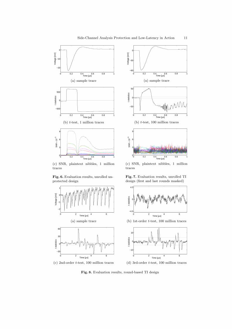
For the unrolled unprotected design, Figure 6 shows a sample power trace,the t-test result as well as the SNR over all 16 plaintext nibbles. Since thedesign is not masked, the t-test as expected shows a pretty strong first-orderleakage. Along the same lines, the corresponding SNR exhibit a clear dependencybetween the traces and the plaintext nibbles. Hence, a successful key-recoveryattack is expected (e.g., in [51]). We should here note that 23.3 mV power peak isrelatively large7 for this low-power FPGA. Since several gates are packed into oneLUT, the equivalent design in ASIC can be more glitchy, and hence (probably)more energy consuming8. This may harden the development of fully unrolled(even low-latency) designs into low-energy, e.g., battery-powered, applications(see simulation-based results in [3] and [4]).
We have shown the corresponding results of the unrolled TI design in Fig-ure 7. As stated before, only the first and the last rounds are masked by meansof four shares (see Figure 3). During the measurements, the 4-share input as wellas other 3 independent fresh random masks (m1, m2, m3 for the last round) aregiven to the Kintex-7 FPGA. The output is also provided in a 4-share maskedform. As discussed before, since the middle rounds are not masked, we expectedthat the t-test exhibits first-order leakage. However, the SNR over plaintextnibbles shows a significant reduction, a factor of about 0.03, compared to theunrolled unprotected design (Figure 6(c) vs. Figure 7(c)). It indeed gives animpression that the first-order attacks on the first round are expect to be chal-lenging. However, if the attacker fixes certain plaintext parts, he can target thesecond cipher round, which is not masked.
7 We showed real voltage values, i.e., output of the amplifier divided by 10.8 This is a guess by the authors and should be examined in practice
Side-Channel Analysis Protection and Low-Latency in Action 11
0 0.2 0.4 0.6 0.8 1
−20
−10
0
Time [μs]
Vol
tage
[mV
]
(a) sample trace
0 0.2 0.4 0.6 0.8 1
0
500
−500
Time [μs]
t sta
tistic
s
(b) t-test, 1 million traces
0 0.2 0.4 0.6 0.8 10
3
6
9
Time [μs]
SN
R ×
10−
3
(c) SNR, plaintext nibbles, 1 milliontraces
Fig. 6. Evaluation results, unrolled un-protected design
0 0.2 0.4 0.6 0.8 1
−30
−60
0
Time [μs]
Vol
tage
[mV
]
(a) sample trace
0 0.2 0.4 0.6 0.8 1
0
50
−50
Time [μs]
t sta
tistic
s
(b) t-test, 100 million traces
0 0.2 0.4 0.6 0.8 10
3
6
9
Time [μs]
SN
R ×
10−
5
(c) SNR, plaintext nibbles, 1 milliontraces
Fig. 7. Evaluation results, unrolled TIdesign (first and last rounds masked)
0 2 4 6
0
1
−2
−1
Time [μs]
Vol
tage
[mV
]
(a) sample trace
0 2 4 6
0
−4.5
4.5
Time [μs]
t sta
tistic
s
(b) 1st-order t-test, 100 million traces
0 2 4 6
0
−30
60
30
Time [μs]
t sta
tistic
s
(c) 2nd-order t-test, 100 million traces
0 2 4 6
0
−10
10
Time [μs]
t sta
tistic
s
(d) 3rd-order t-test, 100 million traces
Fig. 8. Evaluation results, round-based TI design
12
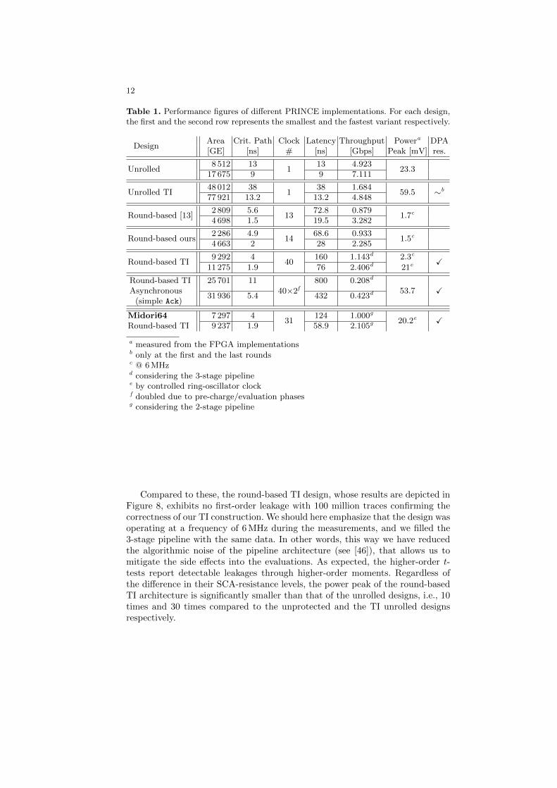
Table 1. Performance figures of different PRINCE implementations. For each design,the first and the second row represents the smallest and the fastest variant respectively.
DesignArea Crit. Path Clock Latency Throughput Powera DPA[GE] [ns] # [ns] [Gbps] Peak [mV] res.
Unrolled8 512 13
113 4.923
23.317 675 9 9 7.111
Unrolled TI48 012 38
138 1.684
59.5 ∼b
77 921 13.2 13.2 4.848
Round-based [13]2 809 5.6
1372.8 0.879
1.7c
4 698 1.5 19.5 3.282
Round-based ours2 286 4.9
1468.6 0.933
1.5c
4 663 2 28 2.285
Round-based TI9 292 4
40160 1.143d 2.3c
X11 275 1.9 76 2.406d 21e
Round-based TIAsynchronous
(simple Ack)
25 701 1140×2f
800 0.208d
53.7 X31 936 5.4 432 0.423d
Midori64 7 297 431
124 1.000g
20.2e XRound-based TI 9 237 1.9 58.9 2.105g
a measured from the FPGA implementationsb only at the first and the last roundsc @ 6 MHzd considering the 3-stage pipelinee by controlled ring-oscillator clockf doubled due to pre-charge/evaluation phasesg considering the 2-stage pipeline
Compared to these, the round-based TI design, whose results are depicted inFigure 8, exhibits no first-order leakage with 100 million traces confirming thecorrectness of our TI construction. We should here emphasize that the design wasoperating at a frequency of 6 MHz during the measurements, and we filled the3-stage pipeline with the same data. In other words, this way we have reducedthe algorithmic noise of the pipeline architecture (see [46]), that allows us tomitigate the side effects into the evaluations. As expected, the higher-order t-tests report detectable leakages through higher-order moments. Regardless ofthe difference in their SCA-resistance levels, the power peak of the round-basedTI architecture is significantly smaller than that of the unrolled designs, i.e., 10times and 30 times compared to the unprotected and the TI unrolled designsrespectively.

Side-Channel Analysis Protection and Low-Latency in Action 13
4 Asynchronous Design
We have already discussed in Section 1 that low-latency concept is closely con-nected to the unrolled (single-cycle) architecture since the high clock rates(needed to rapidly run register-based designs) are not available or supported bymany systems. For instance, in many FPGA designs clock rates above 200 MHzare often difficult to realize. In this settings, asynchronous circuits seem to bean alternative to this issue. With asynchronous circuit design, also known asself-timed and clock-less design, it is possible to realize circuits with high per-formance parameters in terms of their power, throughput, electromagnetic emis-sions, etc. [39,45]. Asynchronous design is not as well-established and widely-usedas synchronous design methodology. Hence, the standard tools for asynchronousdesign are not available, or not widely known, or particularly customized forcertain technologies.
Because the field of asynchronous circuit design covers a wide range, wefocus only on certain concepts which are relevant to our case studies. In termsof PRINCE, consider the round-based synchronous architecture in Figure 4(a).The maximum clock frequency is defined by the longest critical path (most likelywhen both Sbox and its inverse are active). However, such a path is not alwaysactive. In other words, in all clock cycles except the middle one the design can beclocked faster. If this design is realized by asynchronous design methodology, theend of the computation of one cipher round initiates the start of the next round.Hence, the design operates at its maximum speed, or let say with its lowestlatency. In this case – similar to the unrolled architectures – the time when thecomputations are finished, i.e., the ciphertext is ready to be read, depends onthe given inputs, but the maximum latency can be estimated.
As shown in Section 3, the round-based TI design can provide the first-orderresistance, but it needs a clock with a frequency between 250 MHz and 500 MHzto achieve the highest throughput (see Table 1). Hence, our objective in thissection is to realize the round-based TI design with an asynchronous designmethodology.
State of the art. We should emphasize that the asynchronous design has beenpreviously applied as a sole SCA countermeasure. One of the earlier works [33]describes a smartcard chip which relies on self-timed circuits to provide pro-tection against physical attacks. The authors proposed to solely use dual-railencoding to reduce the threat of data-dependent power consumption but alsonoted the obvious difficulties of this approach, e.g., varying wire lengths. Further-more, they highlighted the problem of timing leakage of asynchronous circuitsand advise to minimize data dependent gate delays coupled with the insertion ofdummy delays to reduce this leakage. Later in [23] the security of a similar self-timed circuit has thoroughly been tested in practice. The authors found thatsmall imbalances in the dual-rail circuits cause data-dependent leakage whichenables an attacker to perform a successful DPA on the asynchronous circuit.They showed that their asynchronous design alone is not sufficient to prevent

14
SCA attacks, and that these imbalances need to be eliminated during the de-sign process to increase the level of security. This is in line with [30, 53] wheresome of the difficulties, e.g., no global clock, with respect to performing DPA onasynchronous designs are described.
One of the first clock-less implementation of AES was presented in [52]. It alsorelies on power-balancing capability of dual-rail and the absence of a global clockto thwart DPA. The dual-rail circuits were found to be more secure than thesingle-rail one, however this is only based on simulation results and a thoroughpractical evaluation is missing.
Another approach to secure AES using clock-less circuits is presented in [14].It again relies on an asynchronous style called quasi delay insensitive (QDI) whichhas a range of supply voltages. The authors noted the above-mentioned limita-tion of this implementation style with respect to SCA resistance [15]. Therefore,they proposed to lower the supply voltage to reduce the SNR and thwart DPA.However, [14] does not include practical experiments related to this approach.Further techniques [16, 17] have been proposed to harden QDI against DPAbased on the introduction of random timing and path swapping. However, theirefficiency was only evaluated using electrical simulations.
More recently, an AES round function in Null Convention logic - anotherdelay insensitive logic paradigm - has been proposed in [50] in which the SCAresistance has again been only evaluated with simulations.
It should be noted that in a majority of the aforementioned articles SCAresistance was not the sole motivation for asynchronous circuits. Other beneficialproperties include a low-power consumption for embedded devices and some formof an integrated fault tolerant scheme.
What we want to examine here is not the application of asynchronous de-sign to prevent SCA leakages. In short, we do not aim at e.g., realizing theround-based unprotected architecture with asynchronous methodology and ex-amine its SCA resistance. Instead, our goal is to investigate the challenges andoutcomes of implementing a correctly-masked design, e.g., round-based thresholdimplementation (Figure 5), under the concept of asynchronous designs. Such aninvestigation is conducted with the goal of achieving a clock-less design whileit is expected to still satisfy the desired first-order SCA protection due to itsunderlying uniform TI construction.
4.1 Fundamentals
Different parts of an asynchronous circuit need to communicate with each other.For example, the finish of one PRINCE round should initiate the next round. Acouple of different handshaking protocols exist to establish such a communica-tion.
The 4-phase dual-rail protocol encodes the data signals into two wires per bit(see Figure 9). Each logical ‘1’ or ‘0’ is represented by {1,0} or {0,1} respectively,while {0,0} is known as “no data” (or “empty”) and {1,1} as invalid. A transitionfrom one valid coding to another is not allowed, unless an “empty” value is

Side-Channel Analysis Protection and Low-Latency in Action 15
Chapter 2: Fundamentals 11
only memory: the address would be bundled with req and the data would bebundled with ack. These alternatives are explained later in section 7.1.1. In thefollowing sections we will restrict the discussion to push channels.
All the bundled-data protocols rely on delay matching, such that the orderof signal events at the sender’s end is preserved at the receiver’s end. On apush channel, data is valid before request is set high, expressed formally asV alid(Data) ≺ Req. This ordering should also be valid at the receiver’s end,and it requires some care when physically implementing such circuits. Possiblesolutions are:
To control the placement and routing of the wires, possibly by routing allsignals in a channel as a bundle. This is trivial in a tile-based datapathstructure.
To have a safety margin at the sender’s end.
To insert and/or resize buffers after layout (much as is done in today’ssynthesis and layout CAD tools).
An alternative is to use a more sophisticated protocol that is robust to wiredelays. In the following sections we introduce a number of such protocols thatare completely insensitive to delays.
2.1.2 The 4-phase dual-rail protocolThe 4-phase dual-rail protocol encodes the request signal into the data signals
using two wires per bit of information that has to be communicated, figure 2.2.In essence it is a 4-phase protocol using two request wires per bit of informationd; one wire d .t is used for signaling a logic 1 (or true), and another wire d .fis used for signaling logic 0 (or false). When observing a 1-bit channel onewill see a sequence of 4-phase handshakes where the participating “request”signal in any handshake cycle can be either d .t or d .f . This protocol is very
"1""0" "E"
dual-rail(push) channel
0
011
d.t d.f
0
101
Valid "0"Valid "1"Not used
Empty ("E")2n
Ack
Data, Req4-phase
Data {d.t, d.f} Empty Valid Empty Valid
Ack
Figure 2.2. A delay-insensitive channel using the 4-phase dual-rail protocol.Fig. 9. A delay-insensitive 4-phase dual-rail protocol (taken from [45])
2n
1
n
1
.
.
n
1
.
.
n
Ackp
Acke
Ack
Ackp
Acke
Ack
SR-latch
2n
Ack
delay
longest
2k+1
done clk reset
reset
done
clk
(a) Ack over all dual rails
2n
1
n
1
.
.
n
1
.
.
n
Ackp
Acke
Ack
Ackp
Acke
Ack
SR-latch
2n
Ack
delay
longest
2k
enable clk reset
reset
enable
clk
(b) Simple Ack
2n
1
n
1
.
.
n
1
.
.
n
Ackp
Acke
Ack
Ackp
Acke
Ack
SR-latch
2n
Ack
delay
longest
2k+1
done clk reset
reset
done
clk
(c) Clock Generator
Fig. 10. Exemplary circuits to generate the Ack and clk signals(a) and (b) for asynchronous designs, (c) for a synchronous design
transmitted in-between, that forms a return-to-zero protocol. This protocol isvery robust; two parties can communicate reliably regardless of delays in thewires, i.e., it is delay-insensitive [45].
This concept is very similar to the WDDL logic style [48], which has beendesigned to mitigate SCA leakages. The underlying dual-rail pre-charge logic isthe same encoding; the valid encodings {0,1} and {1,0} are known as evaluationphase and the empty value {0,0} as pre-charge phase. A WDDL circuit is usuallya synchronous design, where the evaluation/pre-charge phases are controlled bythe clock signal (the same concept as in Figure 9 by replacing the Ack signalwith clock). This protocol is familiar to most digital designers, and avoids anyglitches in the circuit hence achieving a low-power construction. However, it hasa disadvantage due to the extra return-to-zero transitions that cost time andenergy.
We can implement the combinatorial parts of a design based on the WDDLconcept, and add extra logic to detect the end of the pre-charge as well asevaluation phase. This allows us to form the Ack signal (see Figure 9). As shownin Figure 10(a), we can integrate n 2-input NOR gates, each of which for a dual-rail signal, and by means of an n-input AND and an n-input NOR gate9 wecan generate Ackp and Acke respectively. When all n dual-rail signals are in pre-charge phase (resp. in evaluation phase), it can be detected by observing Ackp
9 Such large gates are made by cascading the smaller gates.

16
(resp. Acke). These two signals can drive an SR-latch to generate the desiredAck signal.
4.2 Asynchronous Round-based TI
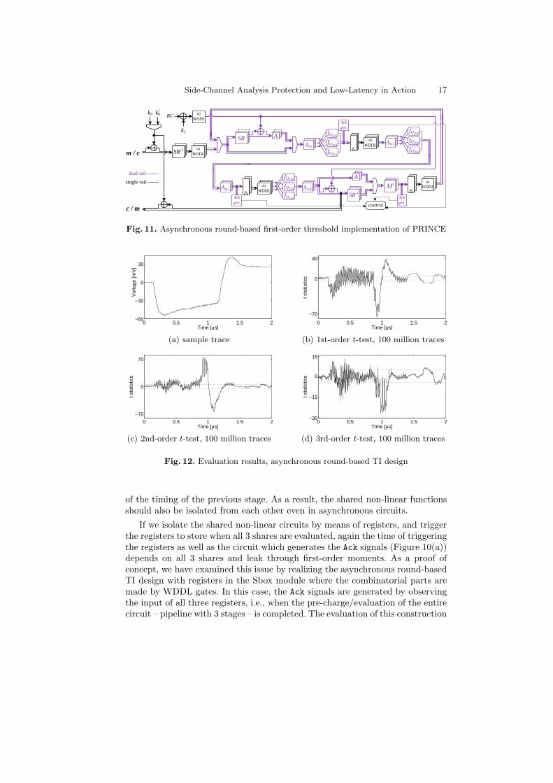
WDDL combinatorial circuits (generally asynchronous circuits) are glitch free,i.e., each dual-rail signal changes only once at each pre-charge/evaluation phase.Threshold implementation has been developed mainly for glitchy circuits, andthe registers should be placed between the non-linear shared functions to avoidthe propagation of the glitches [40]. Hence, at the first glance it seems that it isnot essential anymore to instantiate such registers if the circuit is glitch free.
Following this concept, we have implemented the round-based TI design pre-sented in Figure 11, and did not integrate registers between the shared Q294
functions. The state register is moved to the end of the round function, andthe Ack signal is generated based on the state register input. By a couple ofengineering tricks the design is mapped to our FPGA platform. We should hereemphasize that Xilinx FPGAs are developed yet only for synchronous designs,and integration of asynchronous circuits is neither straightforward nor efficient.For example, each dual-rail WDDL gate should be implemented by a LUT [5].
Our design is a self-timed circuit, i.e., it does not require an external clock,and once the reset signal goes LO, the circuit starts the first evaluation phase,which is the first PRINCE round. Controlled by the internally-generated Ack sig-nal, the end of the evaluation phase triggers the state register to save the cipherstate and simultaneously the start of the pre-charge phase. As stated before, adisadvantage of such a concept is its required interleaved pre-charge/evaluationphases. Because we avoided the extra registers within the Sbox, the design doesnot form a pipeline anymore. Therefore, a full PRINCE is performed by 14(pre-charge, evaluation) cycles. Figure 12 shows a sample power trace of such adesign, where the cipher rounds can be identified. However, the t-test indicatesa pretty strong first-order leakage. Note that the design still realizes a uniformthreshold implementation with 3 shares, and we have not used WDDL as anSCA countermeasure, rather as a 4-phase dual-rail protocol to enable detectionof the end of the evaluation (and pre-charge) of the combinatorial circuit.
A more careful investigation about the detected first-order leakage clarifiedthat although the circuit is glitch free, the non-linear circuits are cascaded. One ofthe component functions of the second non-linear circuit (the second shared Q294
in Figure 11) starts to evaluate when two output shares of the first non-linearcircuit are both evaluated. Further, these two shares depend on all three sharesof the Sbox input. Therefore, the start of the evaluation of the second non-linearcircuit depends on all three input shares of the Sbox. This, which is a non-linearcondition (i.e., when both two output shares of the first non-linear circuit areevaluated) is the reason for such a detectable first-order leakage (see [23] for asimilar experience on an unmasked design). Although placing registers betweenthe shared non-linear functions was initially introduced to avoid the propagationof glitches, it also synchronizes the start of their evaluation to be independent
Side-Channel Analysis Protection and Low-Latency in Action 17
AA
SR-1SR-1SR-1
m / c
RC
k1
k0 k0
A
c / m
SR-1SR-1SR
Ain fQ
fQ
fQ
Am1 fQ
fQ
fQ
Am2 fQ
fQ
fQ
AoutSR-1SR-1SR-1
AAA
Mʹ
294294
294
294
294
294
294
294
294
to
WDDL
to
WDDL
to
WDDL
Ack
gen.
to
WDDL
to
WDDL
Ack
gen.control
Ack
gen.
dual-rail
single-rail
Fig. 11. Asynchronous round-based first-order threshold implementation of PRINCE
0 0.5 1 1.5 2
0
30
−60
−30
Time [μs]
Vol
tage
[mV
]
(a) sample trace
0 0.5 1 1.5 2
0
−70
40
Time [μs]
t sta
tistic
s
(b) 1st-order t-test, 100 million traces
0 0.5 1 1.5 2
0
−70
70
Time [μs]
t sta
tistic
s
(c) 2nd-order t-test, 100 million traces
0 0.5 1 1.5 2
0
15
−15
−30
Time [μs]
t sta
tistic
s
(d) 3rd-order t-test, 100 million traces
Fig. 12. Evaluation results, asynchronous round-based TI design
of the timing of the previous stage. As a result, the shared non-linear functionsshould also be isolated from each other even in asynchronous circuits.
If we isolate the shared non-linear circuits by means of registers, and triggerthe registers to store when all 3 shares are evaluated, again the time of triggeringthe registers as well as the circuit which generates the Ack signals (Figure 10(a))depends on all 3 shares and leak through first-order moments. As a proof ofconcept, we have examined this issue by realizing the asynchronous round-basedTI design with registers in the Sbox module where the combinatorial parts aremade by WDDL gates. In this case, the Ack signals are generated by observingthe input of all three registers, i.e., when the pre-charge/evaluation of the entirecircuit – pipeline with 3 stages – is completed. The evaluation of this construction

18
0 0.5 1 1.5 2
0
30
−60
−30
Time [μs]
Vol
tage
[mV
]
(a) sample trace
0 0.5 1 1.5 2
0
4.5
−4.5
Time [μs]
t sta
tistic
s
(b) 1st-order t-test, 100 million traces
0 0.5 1 1.5 2
0
6
−8
Time [μs]
t sta
tistic
s
(c) 2nd-order t-test, 100 million traces
0 0.5 1 1.5 2
0
12
−9
Time [μs]
t sta
tistic
s
(d) 3rd-order t-test, 100 million traces
Fig. 13. Evaluation results, asynchronous round-based TI design with simple Ack
has also showed detectable first-order leakage. So, we omit the correspondingresults.
As a side note, the early propagation effect [47] of WDDL aggravates thisissue. In the above explained experiments we have used the noEE version [5] ofWDDL (available only for FPGAs), that avoids early propagation only in evalu-ation phase. We have also made use of its successor, AWDDL [35] (also only forFPGAs) which avoids early propagation in both phases. Regardless of its doublearea requirements, its utilization in our case slightly reduced the first-order leak-age, but could not avoid it due to the known imbalances between the delay ofdual rails. In other words, the time required for full pre-charge/evaluation phaseof non-linear circuits still depends on three shares and hence on unshared input.
Therefore, the only solution which we could consider for a secure design is tosimplify the Ack generator circuit. It means that if we generate the Ack signalbased on only one share of one of the state registers, the start time of the nextpre-charge/evaluation phase should be independent from the unshared values.However, such a circuit cannot guarantee that the pre-charge/evaluation of theother parts of the circuit are also finished. Therefore, we have found a path withthe largest delay and connected the Ack generator circuit accordingly. To ensurethe end of the pre-charge/evaluation of the other circuits, the generated Ack
signal is delayed (see Figure 10(b)).
A sample trace as well as the t-test results are shown in Figure 13, whichconfirms the prevention of first-order leakages. This construction is still a self-timed asynchronous circuit without external clock, but it is vastly customized.For instance, it does not operate at its maximum speed, and controlled mainly

Side-Channel Analysis Protection and Low-Latency in Action 19
0 0.2 0.4 0.6 0.8 1
−20
−10
0
Time [μs]
Vol
tage
[mV
]
(a) sample trace
0 0.2 0.4 0.6 0.8 1
0
4.5
−4.5
Time [μs]
t sta
tistic
s
(b) 1st-order t-test, 100 million traces
0 0.2 0.4 0.6 0.8 1
0
10
−10
Time [μs]
t sta
tistic
s
(c) 2nd-order t-test, 100 million traces
0 0.2 0.4 0.6 0.8 1
0
4.5
−4.5
Time [μs]
t sta
tistic
s
(d) 3rd-order t-test, 100 million traces
Fig. 14. Evaluation results, round-based TI design clocked by a controlled ring oscil-lator
by a delayed periodic signal. Hence, we do not benefit from all the features ofasynchronous methodology. If we ignore the low-power feature of this construc-tion, it is not significantly different from the corresponding synchronous designwith a high speed clock. As we listed in Table 1, the asynchronous design is muchlarger than its synchronous variant. Further, due to the interleaved (pre-charge,evaluation) phases, the latency of the asynchronous design is also not convincing.
The interleaved (pre-charge, evaluation) phases of 4-phase dual-rail protocols(e.g., WDDL which we used here) doubles the latency of the design. Alterna-tively, one can utilize a 2-phase dual-rail protocol [45], where ‘1’ and ‘0’ valuesare encoded as signal transitions. Such protocols lead to faster but much morecomplex circuits. We have applied Level-Encoded Dual-Rail (LEDR) [19] conceptand designed and evaluated the corresponding circuit, but due to the similarityof the results to that of the WDDL, their presentation is omitted. In short, thedesign was much bigger than its WDDL variant, but slightly faster. However,all issues with respect to isolation of non-linear functions as well as the Ack
generator circuit hold true.
In this situation, where the operation of non-linear circuits must be isolatedand independent of other non-linear parts, we believe that the synchronous de-sign is favorable. For the remaining issue, i.e., absence of a fast clock in manyapplications where low-latency cryptography is required, we suggest to generatesuch a clock by means of a ring oscillator. Since the energy consumption of largeclock-trees (operated at a high frequency) is not desirable in many applications,the ring oscillator can be controlled by the start and end of e.g., the encryption

20
module. A schematic view of an exemplary circuit is depicted in Figure 10(c).Obviously the ring oscillator should be adjusted based on the critical path delayof the circuit.
We have practically evaluated such a construction as well, whose results areshown by Figure 14. As expected, higher power consumption peak comparedto the same design operated at 6 MHz (see Figure 8(a)) is observed. However,the first-order leakage is still avoided, and more interestingly the higher-orderleakages are mitigated (Figure 14 vs. Figure 8). The reason is due to the overlapbetween the adjacent power peaks, which leads to higher amount of noise, andconsecutively harder higher-order leakages to detect, e.g., in [38].
5 Discussion
We have discussed and shown that SCA-protected designs (by means of mask-ing) should involve registers even in case of asynchronous designs. Therefore, thelow-latency concept – with a perspective of unrolled architectures – is in contra-diction with masking in hardware. As a result, round-based architectures are theonly possible solution for applications, where provably-secure SCA protection isrequired. In this scenario, in order to achieve a low latency two parameters playthe most important role: i) the latency of each cipher round, and ii) the numberof rounds.
Obviously, the most challenging issue, which we faced, was uniform realiza-tion of the shared Sbox with 3 shares. In the seminal article [13], 8 differentSboxes (up to affine equivalent) are suggested for the PRINCE-family. However,all of them need at least a 3-stage decomposition to be able to uniformly sharedwith 3 shares. Such a decomposition, as shown in Section 3.3, leads to a pipelineround-based architecture with 3 stages. This – as stated above – increases thenumber of clock cycles required for each cipher round, and negatively affect thelatency.
For the future designs, our first suggestion is to select Sboxes, whose uniformsharing needs a low number of stages. The extreme case is to apply quadraticSboxes, which can be shared in one stage, but such a choice leads to highernumber of rounds (see PrintCipher [28]), which affect the low-latency target aswell. Hence, the trade-off here is to select either a quadratic Sbox, which needsmore number of rounds, or a cubic TI-friendly Sbox which forms a pipeline,hence more number of clock cycles per round.
The second challenging issue was to deal with round constants. In case ofPRINCE, the round constants have been selected from a semi-random source(fraction of π = 3.141 . . .). This design decision does not have any performancepenalty in case of unrolled architecture, since a round constant just turns someXOR gates of the prior AddRoundKey to XNOR, i.e., for free10. However,for a round-based design, this leads to a relatively large combinatorial circuitsince each round constant should be selected at each round based on the round
10 2-input XOR and XNOR gates need the same area [43].
Side-Channel Analysis Protection and Low-Latency in Action 21
m / c
c / m
Ain fQ
fQ
fQ
Am fQ
fQ
fQ
Aout
SR-1SR-1SC
MC
12
12
12
12
12
12
S
SR-1SR-1
SC
-1
k0
k1
αi
Fig. 15. Round-based first-order threshold implementation of Midori64
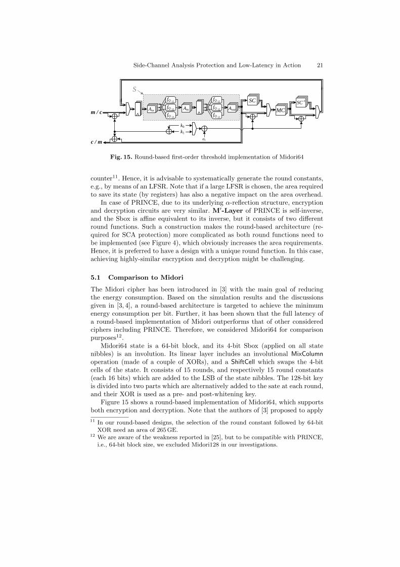
counter11. Hence, it is advisable to systematically generate the round constants,e.g., by means of an LFSR. Note that if a large LFSR is chosen, the area requiredto save its state (by registers) has also a negative impact on the area overhead.
In case of PRINCE, due to its underlying α-reflection structure, encryptionand decryption circuits are very similar. M′-Layer of PRINCE is self-inverse,and the Sbox is affine equivalent to its inverse, but it consists of two differentround functions. Such a construction makes the round-based architecture (re-quired for SCA protection) more complicated as both round functions need tobe implemented (see Figure 4), which obviously increases the area requirements.Hence, it is preferred to have a design with a unique round function. In this case,achieving highly-similar encryption and decryption might be challenging.
5.1 Comparison to Midori
The Midori cipher has been introduced in [3] with the main goal of reducingthe energy consumption. Based on the simulation results and the discussionsgiven in [3, 4], a round-based architecture is targeted to achieve the minimumenergy consumption per bit. Further, it has been shown that the full latency ofa round-based implementation of Midori outperforms that of other consideredciphers including PRINCE. Therefore, we considered Midori64 for comparisonpurposes12.
Midori64 state is a 64-bit block, and its 4-bit Sbox (applied on all statenibbles) is an involution. Its linear layer includes an involutional MixColumnoperation (made of a couple of XORs), and a ShiftCell which swaps the 4-bitcells of the state. It consists of 15 rounds, and respectively 15 round constants(each 16 bits) which are added to the LSB of the state nibbles. The 128-bit keyis divided into two parts which are alternatively added to the sate at each round,and their XOR is used as a pre- and post-whitening key.
Figure 15 shows a round-based implementation of Midori64, which supportsboth encryption and decryption. Note that the authors of [3] proposed to apply
11 In our round-based designs, the selection of the round constant followed by 64-bitXOR need an area of 265 GE.
12 We are aware of the weakness reported in [25], but to be compatible with PRINCE,i.e., 64-bit block size, we excluded Midori128 in our investigations.

22
0 0.2 0.4 0.6 0.8 1
−20
−10
0
Time [μs]
Vol
tage
[mV
]
(a) sample trace
0 0.2 0.4 0.6 0.8 1
0
4.5
−4.5
Time [μs]
t sta
tistic
s
(b) 1st-order t-test, 100 million traces
0 0.2 0.4 0.6 0.8 1
0
30
60
Time [μs]
t sta
tistic
s
(c) 2nd-order t-test, 100 million traces
0 0.2 0.4 0.6 0.8 1
0
8
16
Time [μs]
t sta
tistic
s
(d) 3rd-order t-test, 100 million traces
Fig. 16. Evaluation results, round-based TI design of Midori64 clocked by a controlledring oscillator
the inverse of the linear operations, i.e., ShiftCell−1 ◦MixColumn, over the roundkeys and round constants for the decryption. However, we found our solution (seeFigure 15) which needs 64 extra 2-input XOR gates, cheaper than the originalsuggestion.
In order to realize its threshold implementation, the linear layers are simplyrepeated over the 3 shares, and a uniform representation of its Sbox is con-structed. The Midori64 Sbox is affine equivalent to C266 class [11], which canbe decomposed to two quadratic bijections with uniform TI. Amongst manypossible solutions we selected Q12 ×Q12 and found affine functions as
S = Aout ◦ Q12 ◦Am ◦ Q12 ◦Ain.
There exist 147 456 such (Ain, Am, Aout) triples, and we selected the followingsettings (with respect to the same criteria explained in Section 3.2):
Ain : 0A1B82934E5FC6D7, e = b, f = a, g = d, h = a+ c,
Am : 84B70C3F95A61D2E, e = b+ d, f = b, g = a, h = 1 + a+ c,
Aout : 8A02DF57CE469B13, e = c, f = a, g = c+ d, h = 1 + b. (4)
The sharing of Q12 : 0123456789CDEFAB with
e = a, f = b+ bd+ cd, g = c+ bd, h = d

Side-Channel Analysis Protection and Low-Latency in Action 23
can be derived by direct sharing [11]. If we define the component functionf i,jQ12
(〈ai, bi, ci, di〉, 〈aj , bj , cj , dj〉) = 〈e, f, g, h〉 as
e = ai, g = bidi + dibj + bidj ,
f = bi + bidi + dibj + bidj + cidi + dicj + cidj , h = di, (5)
we can form a uniform shared representation of Q12 by f2,3Q12(., .), f3,1Q12
(., .) and
f1,2Q12(., .), as shown in Figure 15.
We have also practically examined its SCA resistance by the FPGA proto-type. For comparison purposes we considered only a synchronous version, wherethe clock is provided by a controlled ring oscillator (with the same number ofinverters as in the corresponding PRINCE design). The results (indicating first-order resistance and stronger leakage through higher-order moments comparedto its corresponding PRINCE) are shown in Figure 16, and the performanceresults are listed in Table 1.
5.2 Conclusions
We have presented the results of an extensive study on application of masking,particularly TI, on PRINCE considering its low-latency goal. As given in Ta-ble 1, the asynchronous design is around 2.8 times larger and around 2.6 timesslower than its synchronous variant. Further, an overview about its power con-sumption (FPGA prototype) shows no advantage, even compared to the casewhen the synchronous design operates at a high frequency13. More importantly,we faced several issues regarding its detectable first-order leakage. Finally, thedesign, which could prevent the leakages, was not much structurally different toa synchronous design, whose clock is internally generated.
Based on Table 1, the fastest synchronous round-based TI needs 11 275 GEwhich is in the range of the unprotected unrolled design (8 512 - 17 675 GE).Although its critical path with 1.9 ns delay is around than 4 times shorter thanthat of the fastest unrolled design, its 40 clock cycle latency leads to 76 ns whichis around 8 times more than 9 ns latency of the unrolled design. However, its un-derlying pipeline architecture compensates in terms of throughput to be between2 and 3 times less than the unprotected unrolled designs.
Compared to the synchronous round-based TI of PRINCE, Midori64 is smallerand achieves lower latency (58.9 ns vs. 76 ns for the fastest designs), but theirthroughput are comparable considering the full capacity of the pipelines. Weshould emphasize that most of the suggestions (given above) can be seen in thedesign of Midori: i) the Sbox is an involution and TI friendly, ii) MixColumnis an involution, iii) it consists of only one type of round function, and iv) theround constants are short (16 bits per round) although they cannot be generatedsystematically. However, with respect to [25] our observation is that: there is still
13 Note here the difference between power consumption of equivalent FPGA and ASICcircuits.

24
a gap to fill, i.e., a low-latency cipher, which in addition to the desired crypto-graphic strength, can easily deal with the challenges addressed in this article.In short, the candidate should still achieve a low latency when fully unrolled aswell as in a round-based fashion, and at the same time its masked (TI) round-based variant is efficient in terms of area and latency for the applications, whereprovably-secure SCA protection is required.
Acknowledgment
The authors would like to acknowledge Ventzislav Nikov for his help with thedecomposition process and Alexander Kuhn for his help with implementation ofdifferent asynchronous variants of PRINCE on FPGA. The research in this workwas supported in part by the DFG Research Training Group GRK 1817/1.
A Masked Unrolled Design (only first and last rounds)
To share the Sbox and its inverse with 4 shares, we represented the Sbox asS = A2 ◦ C231 ◦A1 and its inverse as S−1 = A4 ◦ C231 ◦A3 withA1 : EF548932AB10CD76, A2 : 08192A3B4C5D6E7F, A3 : 92386DC7F45E0BA1,A4 : 51736240FBD9C8EA, and C231 : 0123468B59CEDA7F as
e =a+ d+ ac+ ad+ bd+ abc+ bcd
f =b+ ac+ bc+ bd+ abd
g =c+ d+ bc+ ad+ cd+ abd+ bcd
h =bc+ ad+ bd+ cd+ abd+ acd+ bcd.
By applying direct sharing on C231 we reach the component functionf i,j,kC231 (〈ai, bi, ci, di〉, 〈aj , bj , cj , dj〉, 〈ak, bk, ck, dk〉) = 〈e, f, g, h〉 as
e =ai + di + aici + aicj + aick + ajci + aidi + aidj + aidk + ajdi + bidi+
bidj + bidk + bjdi + aibici + aibjck + aibkcj + ajbick + ajbkci+
akbicj + akbjci + aibicj + aibjcj + aibick + aibkck + ajbjci+
ajbici + aibjci + aibkci + ajbicj + bicidi + bicjdk + bickdj+
bjcidk + bjckdi + bkcidj + bkcjdi + bicidj + bicjdj + bicidk+
bickdk + bjcjdi + bjcidi + bicjdi + bickdi + bjcidj
f =bi + aici + aicj + aick + ajci + bici + bicj + bick + bjci + bidi + bidj+
bidk + bjdi + aibidi + aibjdk + aibkdj + ajbidk + ajbkdi + akbidj+
akbjdi + aibidj + aibjdj + aibidk + aibkdk + ajbjdi + ajbidi+
aibjdi + aibkdi + ajbidj

Side-Channel Analysis Protection and Low-Latency in Action 25
g =ci + di + bici + bicj + bick + bjci + aidi + aidj + aidk + ajdi + cidi + cidj+
cidk + cjdi + aibidi + aibjdk + aibkdj + ajbidk + ajbkdi + akbidj+
akbjdi + aibidj + aibjdj + aibidk + aibkdk + ajbjdi + ajbidi + aibjdi+
aibkdi + ajbidj + bicidi + bicjdk + bickdj + bjcidk + bjckdi + bkcidj+
bkcjdi + bicidj + bicjdj + bicidk + bickdk + bjcjdi + bjcidi + bicjdi+
bickdi + bjcidj
h =bici + bicj + bick + bjci + aidi + aidj + aidk + ajdi + bidi + bidj + bidk+
bjdi + cidi + cidj + cidk + cjdi + aibidi + aibjdk + aibkdj + ajbidk+
ajbkdi + akbidj + akbjdi + aibidj + aibjdj + aibidk + aibkdk + ajbjdi+
ajbidi + aibjdi + aibkdi + ajbidj + aicidi + aicjdk + aickdj + ajcidk+
ajckdi + akcidj + akcjdi + aicidj + aicjdj + aicidk + aickdk + ajcjdi+
ajcidi + aicjdi + aickdi + ajcidj + bicidi + bicjdk + bickdj + bjcidk+
bjckdi + bkcidj + bkcjdi + bicidj + bicjdj + bicidk + bickdk + bjcjdi+
bjcidi + bicjdi + bickdi + bjcidj
By implementing four instances of this component function f2,3,4C231 (., ., .),
f3,4,1C231 (., ., .), f4,1,2C231 (., ., .), and f1,2,3C231 (., ., .) we reach a correct, non-complete, butnon-uniform sharing of C231. Note that the 64-bit masks m1, m2, and m3 requiredto share the last input round are independent of the masks used to share thecipher input.

26
B Round-based Designs
S -1m / c
RC
S
SR-1Mʹ
RC
SRc / m
k1k1
k1
k1
k0
RC α RC α k0
k0 αʹ
k0 αʹ
(a) Clock cycle 1
S -1m / c
RC
S
SR-1Mʹ
RC
SRc / m
k1k1
k1
k1
k0
RC α RC α k0
k0 αʹ
k0 αʹ
(b) Clock cycles 2-6
S -1m / c
RC
S
SR-1Mʹ
RC
SRc / m
k1k1
k1
k1
k0
RC α RC α k0
k0 αʹ
k0 αʹ
(c) Clock cycle 7
S -1m / c
RC
S
SR-1Mʹ
RC
SRc / m
k1k1
k1
k1
k0
RC α RC α k0
k0 αʹ
k0 αʹ
(d) Clock cycles 8-12
S -1m / c
RC
S
SR-1Mʹ
RC
SRc / m
k1k1
k1
k1
k0
RC α RC α k0
k0 αʹ
k0 αʹ
(e) Clock cycle 13
Fig. 17. Detailed active parts of the original round-based architecture [13]

Side-Channel Analysis Protection and Low-Latency in Action 27
S -1m / c Mʹ
k1k0 k0
SR-1
SR A A
SR-1
c / m
000...000
RCbe5...c6c
c0a...0dd
7ef...cb1
......
count dec
start dec
start
(a) Clock cycle 1
S -1m / c Mʹ
k1k0 k0
SR-1
SR A A
SR-1
c / m
000...000
RCbe5...c6c
c0a...0dd
7ef...cb1...
...
count dec
start dec
start
(b) Clock cycles 2-7
S -1m / c Mʹ
k1k0 k0
SR-1
SR A A
SR-1
c / m
000...000
RCbe5...c6c
c0a...0dd
7ef...cb1
......
count dec
start dec
start
(c) Clock cycles 8-13
S -1m / c Mʹ
k1k0 k0
SR-1
SR A A
SR-1
c / m
000...000
RCbe5...c6c
c0a...0dd
7ef...cb1
......
count dec
start dec
start
(d) Clock cycle 14
Fig. 18. Detailed active parts of our round-based architecture

28
C Decomposition of C231
Table 2. All possible ways to decompose C231 by selected quadratic bijections in threestages
C231 C150 C151 C158 C159 C168 C171 C172 C214 C215 C223 C262 C266 C296 C297Q4 × ×Q12 × × × × × × × × × × × ×Q293 × × × × × × × × × × × × ×Q294 × × × × × × × × × × ×Q299 × × × × × × × × × × × × ×
C150 : Q12 ×Q293
C151 : Q293 ×Q12
C158 : Q299 ×Q293
C159 : Q293 ×Q299
C168 : Q293 ×Q293
C171 : Q293 ×Q12 Q294 ×Q293
C172 : Q12 ×Q293 Q293 ×Q294
C214 :Q4 ×Q299 Q12 ×Q12 Q12 ×Q294 Q12 ×Q299 Q293 ×Q4 Q293 ×Q12
Q293 ×Q294 Q293 ×Q299 Q294 ×Q12 Q294 ×Q294 Q294 ×Q299
C215 :Q4 ×Q293 Q12 ×Q12 Q12 ×Q293 Q12 ×Q294 Q294 ×Q12 Q294 ×Q293
Q294 ×Q294 Q299 ×Q4 Q299 ×Q12 Q299 ×Q293 Q299 ×Q294
Q12 ×Q299 Q293 ×Q293 Q293 ×Q294 Q294 ×Q293 Q294 ×Q294 Q299 ×Q12C223 : Q299 ×Q299
C262 : Q12 ×Q299 Q294 ×Q299 Q299 ×Q12 Q299 ×Q294
C266 : Q12 ×Q12 Q294 ×Q299 Q299 ×Q294 Q299 ×Q299
C296 : Q12 ×Q299 Q293 ×Q293 Q294 ×Q12 Q299 ×Q294 Q299 ×Q299
C297 : Q12 ×Q294 Q293 ×Q293 Q294 ×Q299 Q299 ×Q12 Q299 ×Q299
References
1. Side-channel AttacK User Reference Architecture. http://satoh.cs.uec.ac.jp/
SAKURA/index.html.2. J. Balasch, B. Gierlichs, R. Verdult, L. Batina, and I. Verbauwhede. Power Analysis
of Atmel CryptoMemory - Recovering Keys from Secure EEPROMs. In Topics inCryptology - CT-RSA 2012, volume 7178 of Lecture Notes in Computer Science,pages 19–34. Springer, 2012.
3. S. Banik, A. Bogdanov, T. Isobe, K. Shibutani, H. Hiwatari, T. Akishita, andF. Regazzoni. Midori: A Block Cipher for Low Energy. In ASIACRYPT 2015,volume 9453 of Lecture Notes in Computer Science, pages 411–436. Springer, 2015.
4. S. Banik, A. Bogdanov, and F. Regazzoni. Exploring Energy Efficiency ofLightweight Block Ciphers. In SAC 2015, volume 9566 of Lecture Notes in Com-puter Science, pages 178–194. Springer, 2016.

Side-Channel Analysis Protection and Low-Latency in Action 29
5. S. Bhasin, S. Guilley, F. Flament, N. Selmane, and J. Danger. Countering earlyevaluation: an approach towards robust dual-rail precharge logic. In Workshop onEmbedded Systems Security - WESS 2010, page 6. ACM, 2010.
6. S. Bhasin, S. Guilley, L. Sauvage, and J. Danger. Unrolling Cryptographic Cir-cuits: A Simple Countermeasure Against Side-Channel Attacks. In CT-RSA 2010,volume 5985 of Lecture Notes in Computer Science, pages 195–207. Springer, 2010.
7. B. Bilgin, B. Gierlichs, S. Nikova, V. Nikov, and V. Rijmen. A More Efficient AESThreshold Implementation. In Progress in Cryptology - AFRICACRYPT 2014,volume 8469 of Lecture Notes in Computer Science, pages 267–284. Springer, 2014.
8. B. Bilgin, B. Gierlichs, S. Nikova, V. Nikov, and V. Rijmen. Higher-Order Thresh-old Implementations. In Advances in Cryptology - ASIACRYPT 2014, Part II,volume 8874 of Lecture Notes in Computer Science, pages 326–343. Springer, 2014.
9. B. Bilgin, B. Gierlichs, S. Nikova, V. Nikov, and V. Rijmen. Trade-Offs for Thresh-old Implementations Illustrated on AES. IEEE Trans. on CAD of Integrated Cir-cuits and Systems, 34(7):1188–1200, 2015.
10. B. Bilgin, S. Nikova, V. Nikov, V. Rijmen, and G. Stutz. Threshold Implemen-tations of All 3×3 and 4×4 S-Boxes. In Cryptographic Hardware and EmbeddedSystems - CHES 2012, volume 7428 of Lecture Notes in Computer Science, pages76–91. Springer, 2012.
11. B. Bilgin, S. Nikova, V. Nikov, V. Rijmen, N. Tokareva, and V. Vitkup. Thresholdimplementations of small S-boxes. Cryptography and Communications, 7(1):3–33,2015.
12. A. Bogdanov, L. R. Knudsen, G. Leander, C. Paar, A. Poschmann, M. J. B. Rob-shaw, Y. Seurin, and C. Vikkelsoe. PRESENT: An Ultra-Lightweight Block Cipher.In Cryptographic Hardware and Embedded Systems - CHES 2007, volume 4727 ofLecture Notes in Computer Science, pages 450–466. Springer, 2007.
13. J. Borghoff, A. Canteaut, T. Guneysu, E. B. Kavun, M. Knezevic, L. R. Knudsen,G. Leander, V. Nikov, C. Paar, C. Rechberger, P. Rombouts, S. S. Thomsen,and T. Yalcin. PRINCE - A Low-Latency Block Cipher for Pervasive ComputingApplications - Extended Abstract. In ASIACRYPT 2012, volume 7658 of LectureNotes in Computer Science, pages 208–225. Springer, 2012.
14. G. Bouesse, M. Renaudin, A. Witon, and F. Germain. A clock-less low-voltageaes crypto-processor. In Solid-State Circuits Conference, 2005. ESSCIRC 2005.Proceedings of the 31st European, pages 403–406. IEEE, 2005.
15. G. F. Bouesse, M. Renaudin, S. Dumont, and F. Germain. DPA on quasi delayinsensitive asynchronous circuits: Formalization and improvement. In DATE, pages424–429. IEEE Computer Society, 2005.
16. G. F. Bouesse, M. Renaudin, and G. Sicard. Improving DPA resistance of quasidelay insensitive circuits using randomly time-shifted acknowledgment signals. InVLSI-SoC, volume 240 of IFIP, pages 11–24. Springer, 2005.
17. G. F. Bouesse, G. Sicard, and M. Renaudin. Path swapping method to improveDPA resistance of quasi delay insensitive asynchronous circuits. In CHES, volume4249 of Lecture Notes in Computer Science, pages 384–398. Springer, 2006.
18. J. Cooper, E. Demulder, G. Goodwill, J. Jaffe, G. Kenworthy, and P. Rohatgi.Test Vector Leakage Assessment (TVLA) Methodology in Practice. InternationalCryptographic Module Conference, 2013.
19. M. E. Dean, T. E. Williams, and D. L. Dill. Efficient self-timing with level-encoded2-phase dual-rail (ledr). In Conference on Advanced Research in VLSI, pages 55–70. MIT Press, 1991.

30
20. A. A. Ding, C. Chen, and T. Eisenbarth. Simpler, Faster, and More Robust T-Test Based Leakage Detection. In COSADE 2016, volume 9689 of Lecture Notesin Computer Science, pages 163–183. Springer, 2016.
21. F. Durvaux, F. Standaert, and S. M. D. Pozo. Towards Easy Leakage Certification.In CHES 2016, volume 9813 of Lecture Notes in Computer Science, pages 40–60.Springer, 2016.
22. T. Eisenbarth, T. Kasper, A. Moradi, C. Paar, M. Salmasizadeh, and M. T. M.Shalmani. On the Power of Power Analysis in the Real World: A Complete Breakof the KeeLoqCode Hopping Scheme. In Advances in Cryptology - CRYPTO 2008,volume 5157 of Lecture Notes in Computer Science, pages 203–220. Springer, 2008.
23. J. J. A. Fournier, S. W. Moore, H. Li, R. D. Mullins, and G. S. Taylor. Securityevaluation of asynchronous circuits. In CHES, volume 2779 of Lecture Notes inComputer Science, pages 137–151. Springer, 2003.
24. G. Goodwill, B. Jun, J. Jaffe, and P. Rohatgi. A testing method-ology for side channel resistance validation. In NIST non-invasiveattack testing workshop, 2011. http://csrc.nist.gov/news_events/
non-invasive-attack-testing-workshop/papers/08_Goodwill.pdf.25. J. Guo, J. Jean, I. Nikolic, K. Qiao, Y. Sasaki, and S. M. Sim. Invariant Subspace
Attack Against Full Midori64. Cryptology ePrint Archive, Report 2015/1189, 2015.http://eprint.iacr.org/.
26. J. Kilian and P. Rogaway. How to Protect DES Against Exhaustive Key Search. InCRYPTO 1996, volume 1109 of Lecture Notes in Computer Science, pages 252–267.Springer, 1996.
27. M. Knezevic, V. Nikov, and P. Rombouts. Low-Latency Encryption - Is”Lightweight = Light + Wait”? In CHES 2012, volume 7428 of Lecture Notesin Computer Science, pages 426–446. Springer, 2012.
28. L. R. Knudsen, G. Leander, A. Poschmann, and M. J. B. Robshaw. PRINTcipher:A Block Cipher for IC-Printing. In CHES 2010, volume 6225 of Lecture Notes inComputer Science, pages 16–32. Springer, 2010.
29. P. C. Kocher, J. Jaffe, and B. Jun. Differential Power Analysis. In CRYPTO 1999,volume 1666 of Lecture Notes in Computer Science, pages 388–397. Springer, 1999.
30. K. J. Kulikowski, M. Su, A. B. Smirnov, A. Taubin, M. G. Karpovsky, and D. Mac-Donald. Delay insensitive encoding and power analysis: A balancing act. InASYNC, pages 116–125. IEEE Computer Society, 2005.
31. J. Liu, Y. Yu, F. Standaert, Z. Guo, D. Gu, W. Sun, Y. Ge, and X. Xie. SmallTweaks Do Not Help: Differential Power Analysis of MILENAGE Implementationsin 3G/4G USIM Cards. In ESORICS 2015, volume 9326 of Lecture Notes inComputer Science, pages 468–480. Springer, 2015.
32. S. Mangard, E. Oswald, and T. Popp. Power Analysis Attacks: Revealing theSecrets of Smart Cards. Springer, 2007.
33. S. W. Moore, R. D. Mullins, P. A. Cunningham, R. J. Anderson, and G. S. Taylor.Improving smart card security using self-timed circuits. In ASYNC, pages 211–218.IEEE Computer Society, 2002.
34. A. Moradi, A. Barenghi, T. Kasper, and C. Paar. On the vulnerability of FPGAbitstream encryption against power analysis attacks: extracting keys from xilinxVirtex-II FPGAs. In ACM Conference on Computer and Communications Security- CCS 2011, pages 111–124. ACM, 2011.
35. A. Moradi and V. Immler. Early Propagation and Imbalanced Routing, How toDiminish in FPGAs. In CHES 2014, volume 5984 of Lecture Notes in ComputerScience, pages 598–615. Springer, 2014.

Side-Channel Analysis Protection and Low-Latency in Action 31
36. A. Moradi, O. Mischke, and C. Paar. Practical evaluation of DPA countermeasureson reconfigurable hardware. In HOST 2011, pages 154–160. IEEE, 2011.
37. A. Moradi, A. Poschmann, S. Ling, C. Paar, and H. Wang. Pushing the Limits: AVery Compact and a Threshold Implementation of AES. In Advances in Cryptology- EUROCRYPT 2011, volume 6632 of Lecture Notes in Computer Science, pages69–88. Springer, 2011.
38. A. Moradi and A. Wild. Assessment of Hiding the Higher-Order Leakages inHardware - What Are the Achievements Versus Overheads? In CHES 2015, volume9293 of Lecture Notes in Computer Science, pages 453–474. Springer, 2015.
39. C. J. Myers. Asynchronous Circuit Design. Wiley, 2001.40. S. Nikova, V. Rijmen, and M. Schlaffer. Secure Hardware Implementation of Non-
linear Functions in the Presence of Glitches. J. Cryptology, 24(2):292–321, 2011.41. D. Oswald and C. Paar. Breaking Mifare DESFire MF3ICD40: Power Analysis
and Templates in the Real World. In CHES 2011, volume 6917 of Lecture Notesin Computer Science, pages 207–222. Springer, 2011.
42. A. Poschmann, A. Moradi, K. Khoo, C. Lim, H. Wang, and S. Ling. Side-ChannelResistant Crypto for Less than 2, 300 GE. J. Cryptology, 24(2):322–345, 2011.
43. A. Y. Poschmann. Lightweight Cryptography: Cryptographic Engineering for aPervasive World. PhD thesis, Ruhr University Bochum, 2009.
44. T. Schneider and A. Moradi. Leakage Assessment Methodology - A Clear Roadmapfor Side-Channel Evaluations. In CHES, volume 9293 of Lecture Notes in ComputerScience, pages 495–513. Springer, 2015.
45. J. Spars and S. Furber. Principles of Asynchronous Circuit Design: A SystemsPerspective. Springer Publishing Company, Incorporated, 1st edition, 2010.
46. F. Standaert, S. B. Ors, and B. Preneel. Power Analysis of an FPGA: Implemen-tation of Rijndael: Is Pipelining a DPA Countermeasure? In CHES 2004, volume3156 of Lecture Notes in Computer Science, pages 30–44. Springer, 2004.
47. D. Suzuki and M. Saeki. Security Evaluation of DPA Countermeasures Using Dual-Rail Pre-charge Logic Style. In Cryptographic Hardware and Embedded Systems -CHES 2006, volume 4249 of Lecture Notes in Computer Science, pages 255–269.Springer, 2006.
48. K. Tiri and I. Verbauwhede. A Logic Level Design Methodology for a Secure DPAResistant ASIC or FPGA Implementation. In Design, Automation and Test inEurope - DATE 2004, pages 246–251. IEEE Computer Society, 2004.
49. Virtual Silicon Inc. 0.18 µm VIP Standard Cell Library Tape Out Ready, PartNumber: UMCL18G212T3, Process: UMC Logic 0.18 µm Generic II Technology:0.18µm, July 2004.
50. J. Wu, Y. Kim, and M. Choi. Low-power side-channel attack-resistant asyn-chronous s-box design for AES cryptosystems. In ACM Great Lakes Symposiumon VLSI, pages 459–464. ACM, 2010.
51. V. Yli-Mayry, N. Homma, and T. Aoki. Improved Power Analysis on UnrolledArchitecture and Its Application to PRINCE Block Cipher. In LightSec 2015,volume 9542 of Lecture Notes in Computer Science, pages 148–163. Springer, 2016.
52. A. Yu and D. S. Bree. A clock-less implementation of the AES resists to powerand timing attacks. In ITCC (2), pages 525–532. IEEE Computer Society, 2004.
53. Z. C. Yu, S. B. Furber, and L. A. Plana. An investigation into the security ofself-timed circuits. In ASYNC, pages 206–215. IEEE Computer Society, 2003.
54. Y. Zhou, Y. Yu, F. Standaert, and J. Quisquater. On the Need of Physical Securityfor Small Embedded Devices: A Case Study with COMP128-1 Implementations inSIM Cards. In Financial Cryptography and Data Security - FC 2013, volume 7859of Lecture Notes in Computer Science, pages 230–238. Springer, 2013.