Embed Size (px)
Citation preview
Rev 1.0 10/14 Copyright © 2014 by Silicon Laboratories Si4x55-C
Si4x55-C
EASY-TO-USE, LOW-CURRENT OOK/(G)FSK SUB-GHZ TRANSCEIVER, TRANSMITTER, AND RECEIVER
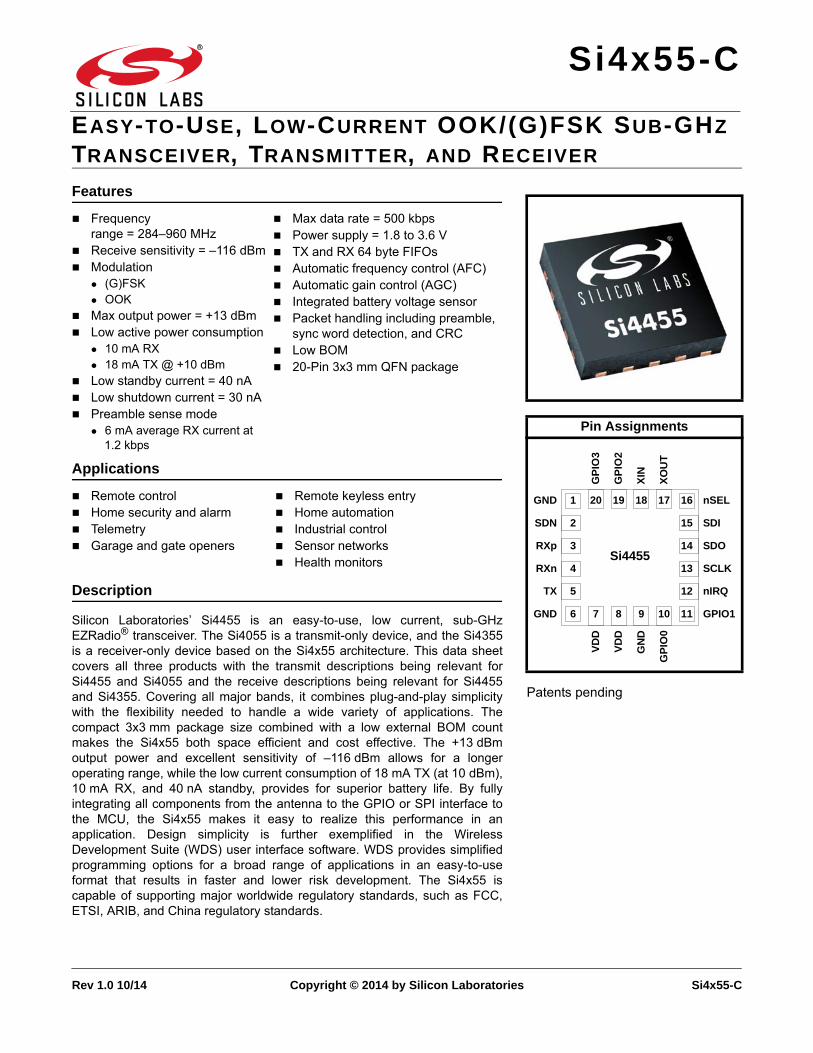
Features
Applications
Description
Silicon Laboratories’ Si4455 is an easy-to-use, low current, sub-GHzEZRadio® transceiver. The Si4055 is a transmit-only device, and the Si4355is a receiver-only device based on the Si4x55 architecture. This data sheetcovers all three products with the transmit descriptions being relevant forSi4455 and Si4055 and the receive descriptions being relevant for Si4455and Si4355. Covering all major bands, it combines plug-and-play simplicitywith the flexibility needed to handle a wide variety of applications. Thecompact 3x3 mm package size combined with a low external BOM countmakes the Si4x55 both space efficient and cost effective. The +13 dBmoutput power and excellent sensitivity of –116 dBm allows for a longeroperating range, while the low current consumption of 18 mA TX (at 10 dBm),10 mA RX, and 40 nA standby, provides for superior battery life. By fullyintegrating all components from the antenna to the GPIO or SPI interface tothe MCU, the Si4x55 makes it easy to realize this performance in anapplication. Design simplicity is further exemplified in the WirelessDevelopment Suite (WDS) user interface software. WDS provides simplifiedprogramming options for a broad range of applications in an easy-to-useformat that results in faster and lower risk development. The Si4x55 iscapable of supporting major worldwide regulatory standards, such as FCC,ETSI, ARIB, and China regulatory standards.
Frequency range = 284–960 MHz
Receive sensitivity = –116 dBm Modulation
(G)FSKOOK
Max output power = +13 dBm Low active power consumption
10 mA RX18 mA TX @ +10 dBm
Low standby current = 40 nA Low shutdown current = 30 nA Preamble sense mode
6 mA average RX current at 1.2 kbps
Max data rate = 500 kbps Power supply = 1.8 to 3.6 V TX and RX 64 byte FIFOs Automatic frequency control (AFC) Automatic gain control (AGC) Integrated battery voltage sensor Packet handling including preamble,
sync word detection, and CRC Low BOM 20-Pin 3x3 mm QFN package
Remote control Home security and alarm Telemetry Garage and gate openers
Remote keyless entry Home automation Industrial control Sensor networks Health monitors
Patents pending
Pin Assignments
1
2
3
4
5
6 7 8 9 10
16
15
14
13
12
11
20 19 18 17GND
SDN
RXp
RXn
TX
GND
nSEL
SDI
SDO
SCLK
nIRQ
GPIO1
VD
D
VD
D
GN
D
GP
IO0
GP
IO3
GP
IO2
XIN
XO
UT
Si4455

Si4x55-C
2 Rev 1.0
Functional Block Diagram
Rx/Tx Modem
Synthesizer
LNA PGA ADC
Rx Chain
PA
SP
I Interface C
ontroller
Battery Voltage Sensor
Aux ADC
25-32MHz XO
SDN
RXp
RXn
TX
VDD GPIO0
GPIO1
nSEL
SDI
SDO
SCLK
nIRQ
XOUTXINGPIO2GPIO3
Si4x55-C
Rev 1.0 3
TABLE OF CONTENTS
Section Page
1. Electrical Specifications . . . . . . . . . . . . . . . . . . . . . . . . . . . . . . . . . . . . . . . . . . . . . . . . . . .42. Typical Applications Schematic . . . . . . . . . . . . . . . . . . . . . . . . . . . . . . . . . . . . . . . . . . . .113. Functional Description . . . . . . . . . . . . . . . . . . . . . . . . . . . . . . . . . . . . . . . . . . . . . . . . . . .12
3.1. Receiver Chain . . . . . . . . . . . . . . . . . . . . . . . . . . . . . . . . . . . . . . . . . . . . . . . . . . . . .133.2. Receiver Modem . . . . . . . . . . . . . . . . . . . . . . . . . . . . . . . . . . . . . . . . . . . . . . . . . . . .133.3. Synthesizer . . . . . . . . . . . . . . . . . . . . . . . . . . . . . . . . . . . . . . . . . . . . . . . . . . . . . . . .143.4. Transmitter . . . . . . . . . . . . . . . . . . . . . . . . . . . . . . . . . . . . . . . . . . . . . . . . . . . . . . . .153.5. Crystal Oscillator . . . . . . . . . . . . . . . . . . . . . . . . . . . . . . . . . . . . . . . . . . . . . . . . . . . .163.6. Battery Voltage and Auxiliary ADC . . . . . . . . . . . . . . . . . . . . . . . . . . . . . . . . . . . . . .16
4. Configuration Options and User Interface . . . . . . . . . . . . . . . . . . . . . . . . . . . . . . . . . . . .174.1. Radio Configuration Application (RCA) GUI . . . . . . . . . . . . . . . . . . . . . . . . . . . . . . .174.2. Configuration Options . . . . . . . . . . . . . . . . . . . . . . . . . . . . . . . . . . . . . . . . . . . . . . . .184.3. Configuration Commands . . . . . . . . . . . . . . . . . . . . . . . . . . . . . . . . . . . . . . . . . . . . .21
5. Controller Interface . . . . . . . . . . . . . . . . . . . . . . . . . . . . . . . . . . . . . . . . . . . . . . . . . . . . . .225.1. Serial Peripheral Interface . . . . . . . . . . . . . . . . . . . . . . . . . . . . . . . . . . . . . . . . . . . . .225.2. Operating Modes and Timing . . . . . . . . . . . . . . . . . . . . . . . . . . . . . . . . . . . . . . . . . .245.3. Interrupts . . . . . . . . . . . . . . . . . . . . . . . . . . . . . . . . . . . . . . . . . . . . . . . . . . . . . . . . . .295.4. GPIO . . . . . . . . . . . . . . . . . . . . . . . . . . . . . . . . . . . . . . . . . . . . . . . . . . . . . . . . . . . . .30
6. Data Handling and Packet Handler . . . . . . . . . . . . . . . . . . . . . . . . . . . . . . . . . . . . . . . . . .316.1. RX and TX FIFOs . . . . . . . . . . . . . . . . . . . . . . . . . . . . . . . . . . . . . . . . . . . . . . . . . . .316.2. Packet Handler . . . . . . . . . . . . . . . . . . . . . . . . . . . . . . . . . . . . . . . . . . . . . . . . . . . . .316.3. Direct Mode . . . . . . . . . . . . . . . . . . . . . . . . . . . . . . . . . . . . . . . . . . . . . . . . . . . . . . . .31
7. Pin Descriptions . . . . . . . . . . . . . . . . . . . . . . . . . . . . . . . . . . . . . . . . . . . . . . . . . . . . . . . . .328. Ordering Information . . . . . . . . . . . . . . . . . . . . . . . . . . . . . . . . . . . . . . . . . . . . . . . . . . . . .349. Package Outline . . . . . . . . . . . . . . . . . . . . . . . . . . . . . . . . . . . . . . . . . . . . . . . . . . . . . . . . .3510. PCB Land Pattern . . . . . . . . . . . . . . . . . . . . . . . . . . . . . . . . . . . . . . . . . . . . . . . . . . . . . . .3711. Top Marking . . . . . . . . . . . . . . . . . . . . . . . . . . . . . . . . . . . . . . . . . . . . . . . . . . . . . . . . . . .38
11.1. Si4x55 Top Marking . . . . . . . . . . . . . . . . . . . . . . . . . . . . . . . . . . . . . . . . . . . . . . . .3811.2. Top Marking Explanation . . . . . . . . . . . . . . . . . . . . . . . . . . . . . . . . . . . . . . . . . . . .38
Contact Information . . . . . . . . . . . . . . . . . . . . . . . . . . . . . . . . . . . . . . . . . . . . . . . . . . . . . . . .39
Si4x55-C
4 Rev 1.0
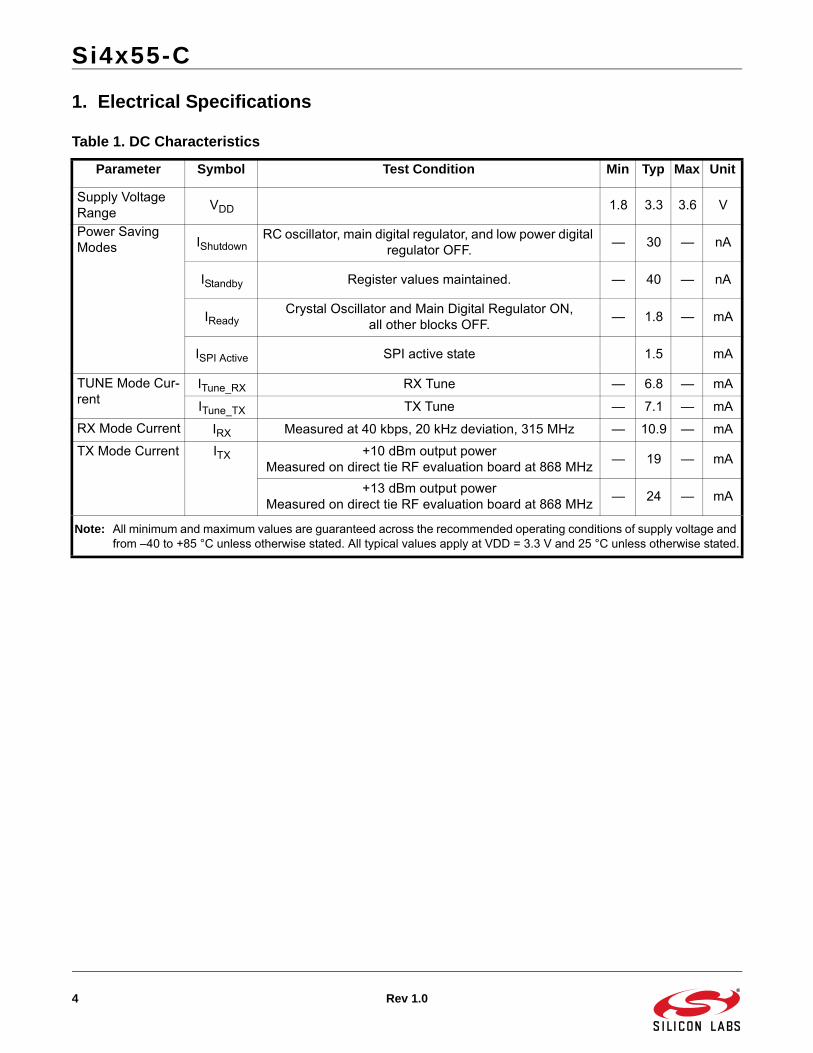
1. Electrical Specifications
Table 1. DC Characteristics
Parameter Symbol Test Condition Min Typ Max Unit
Supply Voltage Range
VDD 1.8 3.3 3.6 V
Power Saving Modes IShutdown
RC oscillator, main digital regulator, and low power digital regulator OFF.
— 30 — nA
IStandby Register values maintained. — 40 — nA
IReadyCrystal Oscillator and Main Digital Regulator ON,
all other blocks OFF. — 1.8 — mA
ISPI Active SPI active state 1.5 mA
TUNE Mode Cur-rent
ITune_RX RX Tune — 6.8 — mA
ITune_TX TX Tune — 7.1 — mA
RX Mode Current IRX Measured at 40 kbps, 20 kHz deviation, 315 MHz — 10.9 — mA
TX Mode Current ITX +10 dBm output powerMeasured on direct tie RF evaluation board at 868 MHz
— 19 — mA
+13 dBm output powerMeasured on direct tie RF evaluation board at 868 MHz
— 24 — mA
Note: All minimum and maximum values are guaranteed across the recommended operating conditions of supply voltage and from –40 to +85 °C unless otherwise stated. All typical values apply at VDD = 3.3 V and 25 °C unless otherwise stated.
Si4x55-C
Rev 1.0 5
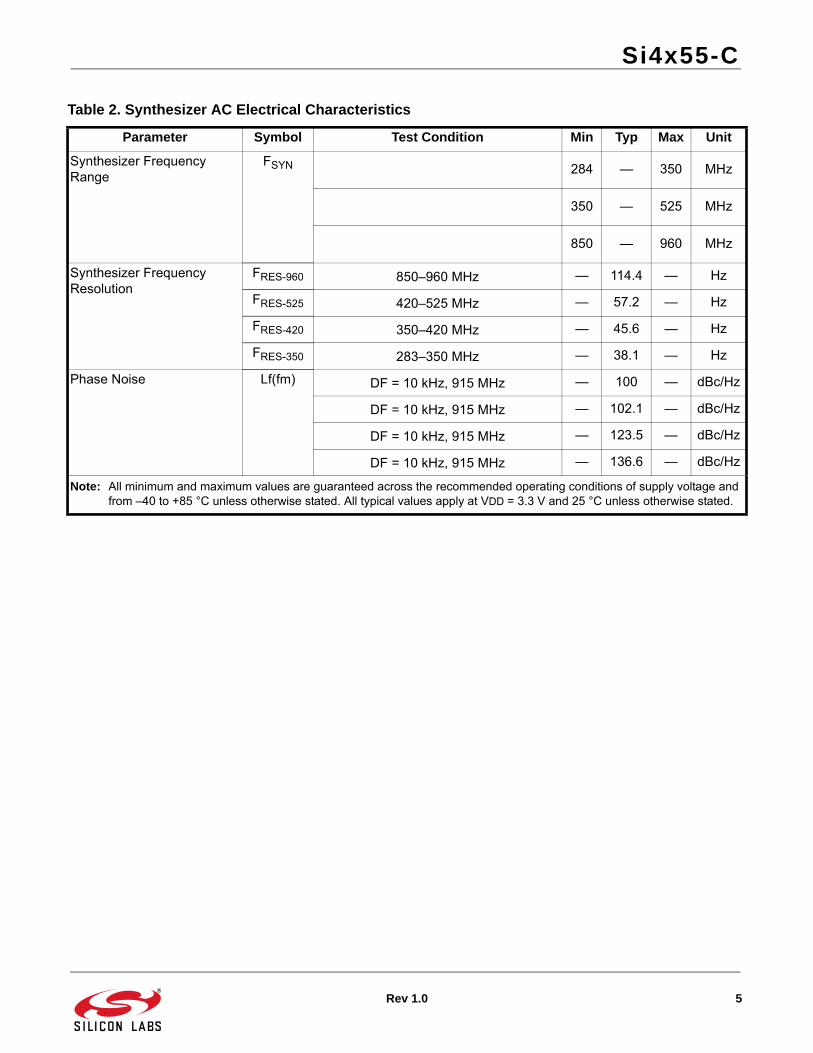
Table 2. Synthesizer AC Electrical Characteristics
Parameter Symbol Test Condition Min Typ Max Unit
Synthesizer FrequencyRange
FSYN 284 — 350 MHz
350 — 525 MHz
850 — 960 MHz
Synthesizer FrequencyResolution
FRES-960 850–960 MHz — 114.4 — Hz
FRES-525 420–525 MHz — 57.2 — Hz
FRES-420 350–420 MHz — 45.6 — Hz
FRES-350 283–350 MHz — 38.1 — Hz
Phase Noise Lf(fm) DF = 10 kHz, 915 MHz — 100 — dBc/Hz
DF = 10 kHz, 915 MHz — 102.1 — dBc/Hz
DF = 10 kHz, 915 MHz — 123.5 — dBc/Hz
DF = 10 kHz, 915 MHz — 136.6 — dBc/Hz
Note: All minimum and maximum values are guaranteed across the recommended operating conditions of supply voltage and from –40 to +85 °C unless otherwise stated. All typical values apply at VDD = 3.3 V and 25 °C unless otherwise stated.

Si4x55-C
6 Rev 1.0
Table 3. Receiver AC Electrical Characteristics
Parameter Symbol Test Condition Min Typ Max Unit
RX FrequencyRange
FRX 284 — 350 MHz
350 — 525 MHz
850 — 960 MHz
RX Sensitivity 915 MHz PRX-_2 (BER < 0.1%)(2.4 kbps, GFSK, BT = 0.5,
F = 30 kHz, 114 kHz Rx BW)2
— –115.0 — dBm
PRX-_40 (BER < 0.1%)(40 kbps, GFSK, BT = 0.5,
F = 25 kHz, 114 kHz Rx BW)2
— –107.6 — dBm
PRX-_128 (BER < 0.1%)(128 kbps, GFSK, BT = 0.5,
F = 70 kHz, 305 kHz Rx BW)2
— –103.2 — dBm
PRX-_OOK (BER < 0.1%, 1 kbps, 185 kHz Rx BW, OOK, PN15 data)2
— –113.5 — dBm
(BER < 0.1%, 40 kbps, 185 kHz Rx BW, OOK, PN15 data)2
— –102.7 — dBm
RX Channel Bandwidth BW 40 — 850 kHz
RSSI Resolution RESRSSI Valid from –110 dBm to –90 dBm — ±0.5 — dB
1-Ch Offset Selectivity2 C/I1-CH Desired Ref Signal 3 dB above sensitiv-ity, BER < 0.1%. Interferer is CW and
desired modulated with 1.2 kbps, F = 5.2 kHz, GFSK with BT = 0.5,
RX BW = 58 kHz channel spacing = 100 kHz
— –52 — dB
2-Ch Offset Selectivity2 C/I2-CH — –56 — dB
Blocking 200 kHz–1 MHz2 200KBLOCK Desired Ref Signal 3 dB above sensitiv-ity, BER < 0.1%. Interferer is CW and
desired modulated with 1.2 kbps F = 5.2 kHz GFSK with BT = 0.5,
RX BW = 58 kHz
— –56 — dB
Blocking 1 MHz Offset2 1MBLOCK — –71 — dB
Blocking 8 MHz Offset2 8MBLOCK — –77 — dB
Image Rejection2 ImREJ Rejection at the image frequency IF = 468 kHz
— 40 — dB
Notes:1. All minimum and maximum values are guaranteed across the recommended operating conditions of supply voltage and
from –40 to +85 °C unless otherwise stated. All typical values apply at VDD = 3.3 V and 25 °C unless otherwise stated.2. Conducted measurements on RF evaluation board. Specifications are dependent on frequency, matching components,
and board layout.
Si4x55-C
Rev 1.0 7
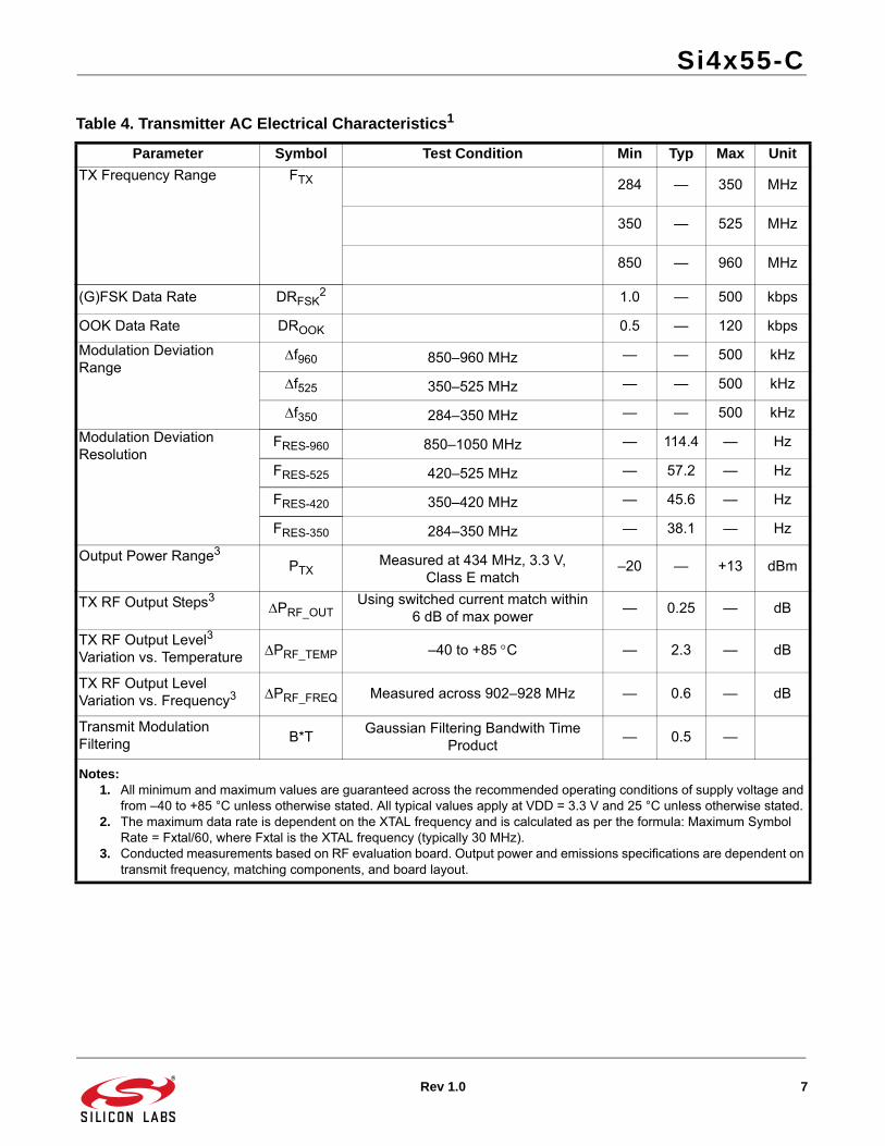
Table 4. Transmitter AC Electrical Characteristics1
Parameter Symbol Test Condition Min Typ Max Unit
TX Frequency Range FTX 284 — 350 MHz
350 — 525 MHz
850 — 960 MHz
(G)FSK Data Rate DRFSK2 1.0 — 500 kbps
OOK Data Rate DROOK 0.5 — 120 kbps
Modulation Deviation Range
f960 850–960 MHz — — 500 kHz
f525 350–525 MHz — — 500 kHz
f350 284–350 MHz — — 500 kHz
Modulation Deviation Resolution
FRES-960 850–1050 MHz — 114.4 — Hz
FRES-525 420–525 MHz — 57.2 — Hz
FRES-420 350–420 MHz — 45.6 — Hz
FRES-350 284–350 MHz — 38.1 — Hz
Output Power Range3PTX
Measured at 434 MHz, 3.3 V, Class E match
–20 — +13 dBm
TX RF Output Steps3PRF_OUT
Using switched current match within 6 dB of max power
— 0.25 — dB
TX RF Output Level3
Variation vs. Temperature PRF_TEMP –40 to +85 C — 2.3 — dB
TX RF Output LevelVariation vs. Frequency3 PRF_FREQ Measured across 902–928 MHz — 0.6 — dB
Transmit Modulation Filtering B*T
Gaussian Filtering Bandwith Time Product
— 0.5 —
Notes:1. All minimum and maximum values are guaranteed across the recommended operating conditions of supply voltage and
from –40 to +85 °C unless otherwise stated. All typical values apply at VDD = 3.3 V and 25 °C unless otherwise stated.2. The maximum data rate is dependent on the XTAL frequency and is calculated as per the formula: Maximum Symbol
Rate = Fxtal/60, where Fxtal is the XTAL frequency (typically 30 MHz).3. Conducted measurements based on RF evaluation board. Output power and emissions specifications are dependent on
transmit frequency, matching components, and board layout.
Si4x55-C
8 Rev 1.0
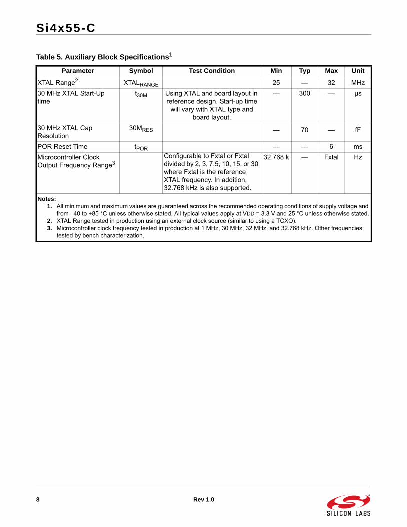
Table 5. Auxiliary Block Specifications1
Parameter Symbol Test Condition Min Typ Max Unit
XTAL Range2 XTALRANGE 25 — 32 MHz
30 MHz XTAL Start-Up time
t30M Using XTAL and board layout in reference design. Start-up time
will vary with XTAL type and board layout.
— 300 — µs
30 MHz XTAL Cap Resolution
30MRES — 70 — fF
POR Reset Time tPOR — — 6 ms
Microcontroller Clock Output Frequency Range3
Configurable to Fxtal or Fxtal divided by 2, 3, 7.5, 10, 15, or 30 where Fxtal is the reference XTAL frequency. In addition, 32.768 kHz is also supported.
32.768 k — Fxtal Hz
Notes:1. All minimum and maximum values are guaranteed across the recommended operating conditions of supply voltage and
from –40 to +85 °C unless otherwise stated. All typical values apply at VDD = 3.3 V and 25 °C unless otherwise stated.2. XTAL Range tested in production using an external clock source (similar to using a TCXO).3. Microcontroller clock frequency tested in production at 1 MHz, 30 MHz, 32 MHz, and 32.768 kHz. Other frequencies
tested by bench characterization.

Si4x55-C
Rev 1.0 9
Table 6. Digital IO Specifications (GPIO_x, SCLK, SDO, SDI, nSEL, nIRQ)1
Parameter Symbol Test Condition Min Typ Max Unit
Rise Time2,3 TRISE 0.1 x VDD to 0.9 x VDD, CL= 10 pF, DRV<1:0> = LL
VDD = 3.3 V
— 2.3 — ns
Fall Time3,4 TFALL 0.9 x VDD to 0.1 x VDD, CL= 10 pF, DRV<1:0> = LL
VDD = 3.3 V
— 2 — ns
Input Capacitance CIN — 2 — pF
Logic High Level Input Voltage VIH VDD x 0.7 — — V
Logic Low Level Input Voltage VIL — — VDD x 0.3 V
Input Current IIN 0 < VIN < VDD –1 — 1 µA
Input Current if Pullup is Activated IINP VIL = 0 V 1 — 4 µA
Drive Strength for Output Low Level
IOmaxLL DRV[1:0] = LL3 — 6.66 — mA
IOmaxLH DRV[1:0] = LH3 — 5.03 — mA
IOmaxHL DRV[1:0] = HL3 — 3.16 — mA
IOmaxHH DRV[1:0] = HH3 — 1.13 — mA
Drive Strength for Output High Level (GPIO1, GPIO2, GPIO3)
IOmaxLL DRV[1:0] = LL3 — 5.75 — mA
IOmaxLH DRV[1:0] = LH3 — 4.37 — mA
IOmaxHL DRV[1:0] = HL3 — 2.73 — mA
IOmaxHH DRV[1:0] = HH3 — 0.96 — mA
Drive Strength for Output High Level (GPIO0)
IOmaxLL DRV[1:0] = LL3 — 2.53 — mA
IOmaxLH DRV[1:0] = LH3 — 2.21 — mA
IOmaxHL DRV[1:0] = HL3 — 1.70 — mA
IOmaxHH DRV[1:0] = HH3 — 0.80 — mA
Logic High Level Output Voltage VOH DRV[1:0] = HL3 VDD x 0.8 — — V
Logic Low Level Output Voltage VOL DRV[1:0] = HL3 — — VDD x 0.2 V
Notes:1. All minimum and maximum values are guaranteed across the recommended operating conditions of supply voltage and
from –40 to +85 °C unless otherwise stated. All typical values apply at VDD = 3.3 V and 25 °C unless otherwise stated.2. 6.7 ns is typical for GPIO0 rise time.3. Assuming VDD = 3.3 V, drive strength is specified at Voh (min) = 2.64 V and Vol (max) = 0.66 V at room temperature.4. 2.4 ns is typical for GPIO0 fall time.
Si4x55-C
10 Rev 1.0
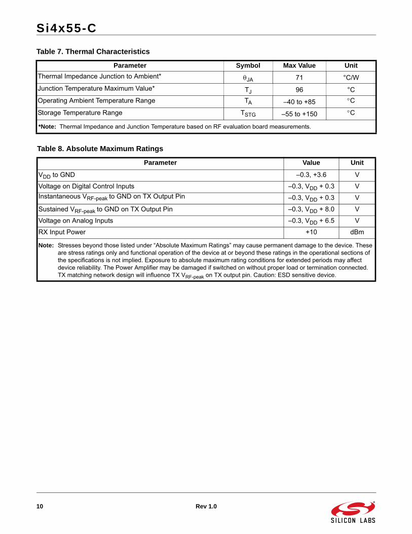
Table 7. Thermal Characteristics
Parameter Symbol Max Value Unit
Thermal Impedance Junction to Ambient* JA 71 °C/W
Junction Temperature Maximum Value* TJ 96 °C
Operating Ambient Temperature Range TA –40 to +85 C
Storage Temperature Range TSTG –55 to +150 C
*Note: Thermal Impedance and Junction Temperature based on RF evaluation board measurements.
Table 8. Absolute Maximum Ratings
Parameter Value Unit
VDD to GND –0.3, +3.6 V
Voltage on Digital Control Inputs –0.3, VDD + 0.3 V
Instantaneous VRF-peak to GND on TX Output Pin –0.3, VDD + 0.3 V
Sustained VRF-peak to GND on TX Output Pin –0.3, VDD + 8.0 V
Voltage on Analog Inputs –0.3, VDD + 6.5 V
RX Input Power +10 dBm
Note: Stresses beyond those listed under “Absolute Maximum Ratings” may cause permanent damage to the device. These are stress ratings only and functional operation of the device at or beyond these ratings in the operational sections of the specifications is not implied. Exposure to absolute maximum rating conditions for extended periods may affect device reliability. The Power Amplifier may be damaged if switched on without proper load or termination connected. TX matching network design will influence TX VRF-peak on TX output pin. Caution: ESD sensitive device.
Si4x55-C
Rev 1.0 11
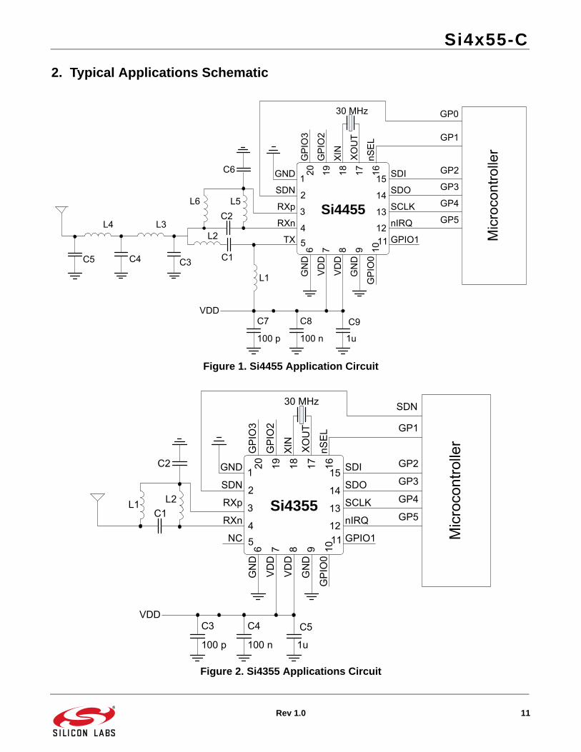
2. Typical Applications Schematic
Figure 1. Si4455 Application Circuit
Figure 2. Si4355 Applications Circuit
30 MHz
Mic
roco
ntro
ller
GP1
GP2
GP3
GP4
C1
L1
L2
GND
GPIO1
19 18 17 16
1
2
3
4
15
14
13
7 8 9 10
SDI
SDO
SCLK
RXn
SDN
RXp
VD
D
VD
D
GP
IO0
XIN
GP
IO3
nSE
L
XO
UT
GN
D
5TX
6G
ND
20
GP
IO2
11
12GP5L4
C2 Si4455nIRQ
VDD
100 n
C8
100 p
C7
1u
L5
C6
C9
L3
C3C4C5
GP0
L6
30 MHz
Mic
roco
ntro
ller
GP1
GP2
GP3
GP4L1
GND
GPIO1
19 18 17 16
1
2
3
4
15
14
13
7 8 9 10
SDI
SDO
SCLK
RXn
SDN
RXp
VD
D
VD
D
GP
IO0
XIN
GP
IO3
nSE
L
XO
UT
GN
D
5NC
6G
ND
20
GP
IO2
11
12GP5C1
Si4355nIRQ
VDD
100 n
C4
100 p
C3
1u
L2
C2
C5
SDN
Si4x55-C
12 Rev 1.0
3. Functional Description
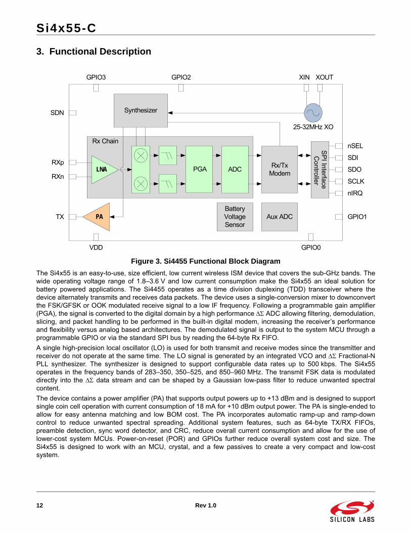
Figure 3. Si4455 Functional Block Diagram
The Si4x55 is an easy-to-use, size efficient, low current wireless ISM device that covers the sub-GHz bands. Thewide operating voltage range of 1.8–3.6 V and low current consumption make the Si4x55 an ideal solution forbattery powered applications. The Si4455 operates as a time division duplexing (TDD) transceiver where thedevice alternately transmits and receives data packets. The device uses a single-conversion mixer to downconvertthe FSK/GFSK or OOK modulated receive signal to a low IF frequency. Following a programmable gain amplifier(PGA), the signal is converted to the digital domain by a high performance ADC allowing filtering, demodulation,slicing, and packet handling to be performed in the built-in digital modem, increasing the receiver’s performanceand flexibility versus analog based architectures. The demodulated signal is output to the system MCU through aprogrammable GPIO or via the standard SPI bus by reading the 64-byte Rx FIFO.
A single high-precision local oscillator (LO) is used for both transmit and receive modes since the transmitter andreceiver do not operate at the same time. The LO signal is generated by an integrated VCO and Fractional-NPLL synthesizer. The synthesizer is designed to support configurable data rates up to 500 kbps. The Si4x55operates in the frequency bands of 283–350, 350–525, and 850–960 MHz. The transmit FSK data is modulateddirectly into the data stream and can be shaped by a Gaussian low-pass filter to reduce unwanted spectralcontent.
The device contains a power amplifier (PA) that supports output powers up to +13 dBm and is designed to supportsingle coin cell operation with current consumption of 18 mA for +10 dBm output power. The PA is single-ended toallow for easy antenna matching and low BOM cost. The PA incorporates automatic ramp-up and ramp-downcontrol to reduce unwanted spectral spreading. Additional system features, such as 64-byte TX/RX FIFOs,preamble detection, sync word detector, and CRC, reduce overall current consumption and allow for the use oflower-cost system MCUs. Power-on-reset (POR) and GPIOs further reduce overall system cost and size. TheSi4x55 is designed to work with an MCU, crystal, and a few passives to create a very compact and low-costsystem.
Rx/Tx Modem
Synthesizer
LNA PGA ADC
Rx Chain
PA
SP
I Interface C
ontroller
Battery Voltage Sensor
Aux ADC
25-32MHz XO
SDN
RXp
RXn
TX
VDD GPIO0
GPIO1
nSEL
SDI
SDO
SCLK
nIRQ
XOUTXINGPIO2GPIO3
Si4x55-C
Rev 1.0 13
3.1. Receiver ChainThe internal low-noise amplifier (LNA) is designed to be a wideband LNA that can be matched with three externaldiscrete components to cover any common range of frequencies in the sub-GHz band. The LNA has extremely lownoise to suppress the noise of the following stages and achieve optimal sensitivity; therefore, no external gain orfront-end modules are necessary. The LNA has gain control, which is controlled by the internal automatic gaincontrol (AGC) algorithm. The LNA is followed by an I-Q mixer, filter, programmable gain amplifier (PGA), and ADC.The I-Q mixers downconvert the signal to an intermediate frequency. The PGA then boosts the gain to be withindynamic range of the ADC. The ADC rejects out-of-band blockers and converts the signal to the digital domainwhere filtering, demodulation, and processing is performed. Peak detectors are integrated at the output of the LNAand PGA for use in the AGC algorithm.
The RX and TX pins can be directly tied externally on the Si4455 transceiver.
3.2. Receiver ModemUsing high-performance ADCs allows channel filtering, image rejection, and demodulation to be performed in thedigital domain, which allows for flexibility in optimizing the device for particular applications. The digital modemperforms the following functions:
Channel selection filter
Preamble detection
Invalid preamble detection
TX modulation
RX demodulation
Automatic Gain Control (AGC)
Automatic frequency compensation (AFC)
Radio signal strength indicator (RSSI)
Cyclic redundancy check (CRC)
The digital channel filter and demodulator are optimized for ultra-low-power consumption and are highlyconfigurable. Supported modulation types are GFSK, FSK, and OOK. The channel filter can be configured tosupport bandwidths ranging from 850 kHz down to 40 kHz. A large variety of data rates are supported ranging from0.5 kbps up to 500 kbps. The configurable preamble detector is used with the synchronous demodulator to improvethe reliability of the sync-word detection. Preamble detection can be skipped using only sync detection, which is avaluable feature of the asynchronous demodulator when very short preambles are used. The received signalstrength indicator (RSSI) provides a measure of the signal strength received on the tuned channel. The resolutionof the RSSI is 0.5 dB. This high-resolution RSSI enables accurate channel power measurements for clear channelassessment (CCA), carrier sense (CS), and listen before talk (LBT) functionality. A wireless communicationchannel can be corrupted by noise and interference, so it is important to know if the received data is free of errors.A cyclic redundancy check (CRC) is used to detect the presence of erroneous bits in each packet. A CRC iscomputed and appended at the end of each transmitted packet and verified by the receiver to confirm that noerrors have occurred. The packet handler and CRC can significantly reduce the load on the system microcontroller,allowing for a simpler and cheaper microcontroller. The digital modem includes the TX modulator, which convertsthe TX data bits into the corresponding stream of digital modulation values to be summed with the fractional inputto the sigma-delta modulator. This modulation approach results in highly accurate resolution of the frequencydeviation. A Gaussian filter is implemented to support GFSK, considerably reducing the energy in adjacentchannels. The default bandwidth-time (BT) product is 0.5 for all programmed data rates.
3.2.1. Received Signal Strength Indicator
The received signal strength indicator (RSSI) is an estimate of the signal strength in the channel to which thereceiver is tuned. The RSSI measurement is done after the channel filter, so it is only a measurement of thedesired or undesired in-band signal power. The Si4x55 uses a fast response register to read RSSI and so cancomplete the read in 16 SPI clock cycles with no requirement to wait for CTS. The RSSI value reported by this APIcommand can be converted to dBm using the following equation:
Si4x55-C
14 Rev 1.0
The value of 130 in the above formula is based on bench characterization of the EZRadio RF Pico boards(evaluation boards). The RSSI value is latched at sync word detection and can be read via the fast responseregister. The latched value of RSSI is available until the device re-enters Rx mode. In addition, the current value ofRSSI can be read out using the GET_MODEM_STATUS command. This can be used to implement CCA (clearchannel assessment) functionality. The user can set up an RSSI threshold value using the WDS RadioConfiguration Application GUI.
3.3. SynthesizerThe Si4x55 includes an integrated Sigma Delta () Fractional-N PLL synthesizer capable of operating over thebands from 283–350, 350–525, and 850–960 MHz. The synthesizer has many advantages; it provides flexibility inchoosing data rate, deviation, channel frequency, and channel spacing. The transmit modulation is applied directlyto the loop in the digital domain through the fractional divider, which results in very precise accuracy and controlover the transmit deviation. The frequency resolution is (2/3)Freq_xo/(219) for 283–350 MHz, Freq_xo/(219) for350–525 MHz, and Freq_xo/(218) for 850–960 MHz. The nominal reference frequency to the PLL is 30 MHz, butany XTAL frequency from 25 to 32 MHz may be used. The modem configuration calculator in WDS willautomatically account for the XTAL frequency being used. The PLL utilizes a differential LC VCO with integratedon-chip inductors. The output of the VCO is followed by a configurable divider, which will divide the signal down tothe desired output frequency band.
3.3.1. Synthesizer Frequency Control
The frequency is set by changing the integer and fractional settings to the synthesizer. The WDS calculator willautomatically provide these settings, but the synthesizer equation is shown below for convenience. Initialfrequency settings are configured in the EZConfig setup and can also be modified using the API commands:FREQ_CONTROL_INTE, FREQ_CONTROL_FRAC2, FREQ_CONTROL_FRAC1, andFREQ_CONTROL_FRAC0.
Note: The fc_frac/219 value in the above formula must be a number between 1 and 2. The LSB of fc_frac must be "1".
3.3.1.1. EZ Frequency Programming
EZ frequency programming allows for easily changing radio frequency using a single API command. The basefrequency is first set using the EZConfig setup. This base frequency will correspond to channel 0. Next, a channelstep size is also programmed within the EZConfig setup. The resulting frequency will be:
The second argument of the START_RX or START_TX is CHANNEL, which sets the channel number for EZfrequency programming. For example, if the channel step size is set to 1 MHz, the base frequency is set to900 MHz, and a CHANNEL number of 5 is programmed during the START_TX command, the resulting frequencywill be 905 MHz. If no CHANNEL argument is written as part of the START_RX/TX command, it will default to theprevious value. The initial value of CHANNEL is 0 and so will be set to the base frequency if this argument is neverused.
Table 9. Output Divider (Outdiv) Values
Outdiv Lower (MHz) Upper (MHz)
12 284 350
10 350 420
8 420 525
4 850 960
RSSIdBmRSSI_value
2--------------------------------- 130–=
RF frequency fc_inte fc_frac
219
------------------+ 4 freq_xo
outdiv------------------------------- Hz =
RF Frequency Base Frequency Channel Step Size+=

Si4x55-C
Rev 1.0 15
3.4. TransmitterThe device contains a +13 dBm power amplifier that is capable of transmitting from –40 to +13 dBm. The outputpower set size is dependent on the power level and can be seen in Figure 4. The PA power level is set using theAPI command: PA_PWR_LVL. The power amplifier is single-ended to allow for easy antenna matching and lowBOM cost. For detailed matching values, BOM, and performance expectations, refer to "AN686: Antennas for theSi4455/4355 RF ICs". Power ramp-up and ramp-down is automatically performed to reduce unwanted spectralspreading.
Figure 4. Tx Power vs PA_PWR_LVL and VDD
Si4x55-C
16 Rev 1.0
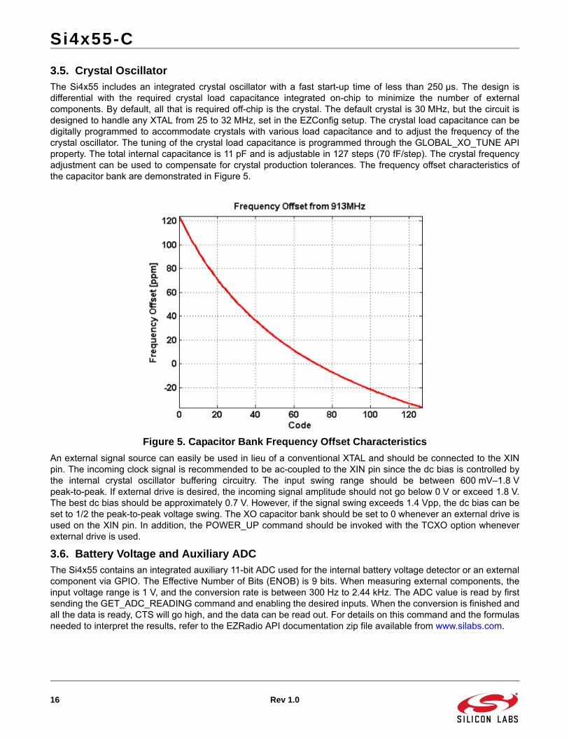
3.5. Crystal OscillatorThe Si4x55 includes an integrated crystal oscillator with a fast start-up time of less than 250 µs. The design isdifferential with the required crystal load capacitance integrated on-chip to minimize the number of externalcomponents. By default, all that is required off-chip is the crystal. The default crystal is 30 MHz, but the circuit isdesigned to handle any XTAL from 25 to 32 MHz, set in the EZConfig setup. The crystal load capacitance can bedigitally programmed to accommodate crystals with various load capacitance and to adjust the frequency of thecrystal oscillator. The tuning of the crystal load capacitance is programmed through the GLOBAL_XO_TUNE APIproperty. The total internal capacitance is 11 pF and is adjustable in 127 steps (70 fF/step). The crystal frequencyadjustment can be used to compensate for crystal production tolerances. The frequency offset characteristics ofthe capacitor bank are demonstrated in Figure 5.
Figure 5. Capacitor Bank Frequency Offset Characteristics
An external signal source can easily be used in lieu of a conventional XTAL and should be connected to the XINpin. The incoming clock signal is recommended to be ac-coupled to the XIN pin since the dc bias is controlled bythe internal crystal oscillator buffering circuitry. The input swing range should be between 600 mV–1.8 Vpeak-to-peak. If external drive is desired, the incoming signal amplitude should not go below 0 V or exceed 1.8 V.The best dc bias should be approximately 0.7 V. However, if the signal swing exceeds 1.4 Vpp, the dc bias can beset to 1/2 the peak-to-peak voltage swing. The XO capacitor bank should be set to 0 whenever an external drive isused on the XIN pin. In addition, the POWER_UP command should be invoked with the TCXO option wheneverexternal drive is used.
3.6. Battery Voltage and Auxiliary ADCThe Si4x55 contains an integrated auxiliary 11-bit ADC used for the internal battery voltage detector or an externalcomponent via GPIO. The Effective Number of Bits (ENOB) is 9 bits. When measuring external components, theinput voltage range is 1 V, and the conversion rate is between 300 Hz to 2.44 kHz. The ADC value is read by firstsending the GET_ADC_READING command and enabling the desired inputs. When the conversion is finished andall the data is ready, CTS will go high, and the data can be read out. For details on this command and the formulasneeded to interpret the results, refer to the EZRadio API documentation zip file available from www.silabs.com.
Si4x55-C
Rev 1.0 17
4. Configuration Options and User Interface
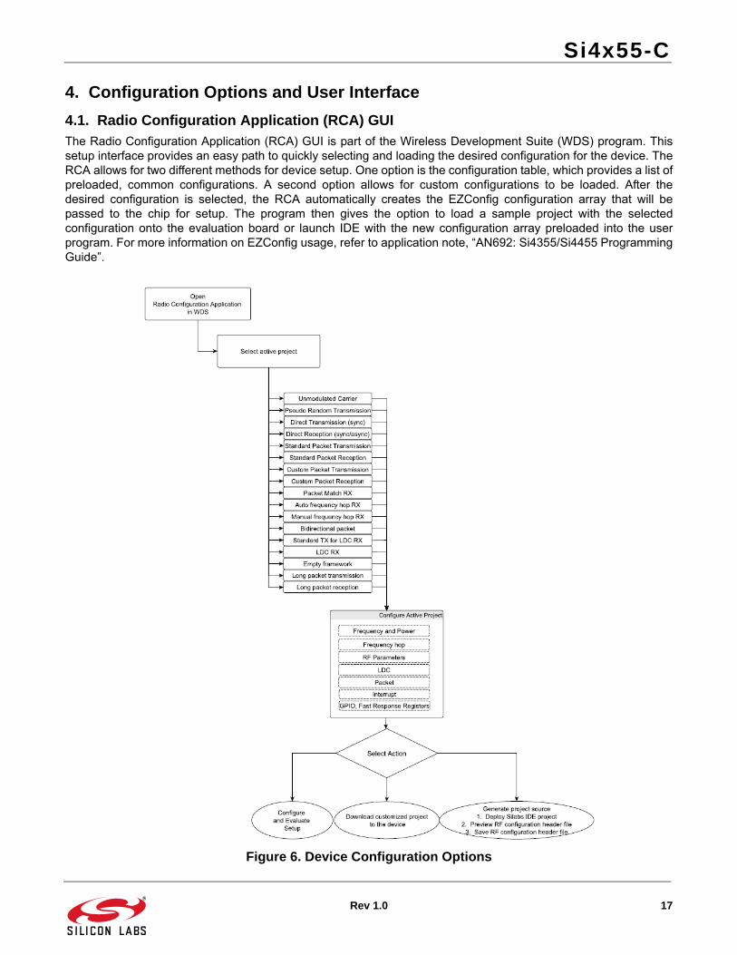
4.1. Radio Configuration Application (RCA) GUIThe Radio Configuration Application (RCA) GUI is part of the Wireless Development Suite (WDS) program. Thissetup interface provides an easy path to quickly selecting and loading the desired configuration for the device. TheRCA allows for two different methods for device setup. One option is the configuration table, which provides a list ofpreloaded, common configurations. A second option allows for custom configurations to be loaded. After thedesired configuration is selected, the RCA automatically creates the EZConfig configuration array that will bepassed to the chip for setup. The program then gives the option to load a sample project with the selectedconfiguration onto the evaluation board or launch IDE with the new configuration array preloaded into the userprogram. For more information on EZConfig usage, refer to application note, “AN692: Si4355/Si4455 ProgrammingGuide”.
Figure 6. Device Configuration Options
Si4x55-C
18 Rev 1.0
4.1.1. Radio Configuration Application
The Radio Configuration Application provides an intuitive interface for directly modifying the device configuration.Using this control panel, the device parameters such as modulation type, data rate, frequency deviation, and anypacket related settings can be set. The program then takes these parameters and automatically determines theappropriate device settings. This method allows the user to have complete flexibility in determining theconfiguration of the device without the need to translate the system requirements into device specific properties.The resulting configuration array is automatically generated and available for use in the user's program. Theresulting configuration array is obfuscated; therefore, its content changes every time a new array is generated,even if the input parameters are the same.
4.2. Configuration Options4.2.1. Frequency Band
The Si4455 can operate in the 283–350 MHz, 350–525 MHz, or 850–960 MHz bands. One of these three bandswill be selected during the configuration setup and then the specific transmission frequency that will be used withinthis band can be selected.
4.2.2. Modulation Type
The Si4x55 can operate using On/Off Keying (OOK), Frequency Shift Keying (FSK), or Gaussian Frequency ShiftKeying (GFSK). OOK modulation is the most basic modulation type available. It is the most power-efficient methodand does not require as high oscillator accuracy as FSK. FSK provides the best sensitivity and range performance,but generally requires more precision from the oscillator used. GFSK is a version of FSK where the signal ispassed through a Gaussian filter, limiting its spectral width. As a result, the out-of-band components of the signalare reduced.
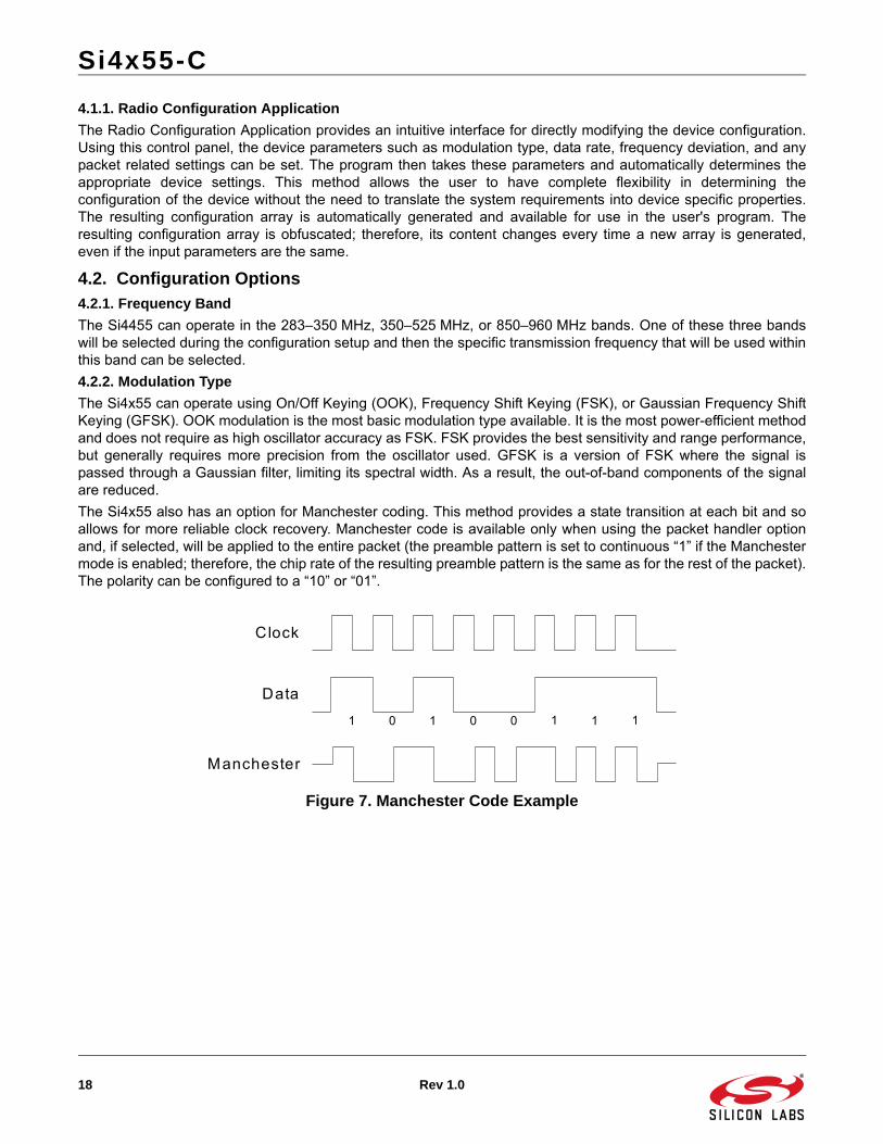
The Si4x55 also has an option for Manchester coding. This method provides a state transition at each bit and soallows for more reliable clock recovery. Manchester code is available only when using the packet handler optionand, if selected, will be applied to the entire packet (the preamble pattern is set to continuous “1” if the Manchestermode is enabled; therefore, the chip rate of the resulting preamble pattern is the same as for the rest of the packet).The polarity can be configured to a “10” or “01”.
Figure 7. Manchester Code Example
1 1 1 1 10 0 0
Clock
Data
Manchester

Si4x55-C
Rev 1.0 19
4.2.3. Frequency Deviation
If FSK or GFSK modulation is selected, then a frequency deviation will also need to be selected. The frequencydeviation is the maximum instantaneous difference between the FM modulated frequency and the nominal carrierfrequency. The Si4x55 can operate across a wide range of data rates and frequency deviations. If a frequencydeviation needs to be selected, the following guideline might be helpful to build a robust link. A proper frequencydeviation is linked to the frequency error between transmitter and receiver. The frequency error can be calculatedusing the crystal tolerance parameters and the RF operating frequency: (ppm_tx+ppm_rx)*Frf/1E-6. For frequencyerrors below 50 kHz, the deviation can be about the same as the frequency error. For frequency errors exceeding50 kHz, the frequency deviation can be set to about 0.75 times the frequency error. It is advised to position themodulation index (= 2*freq_dev/data_rate) into a range between 1 and 100 for Packet Handling mode and 2 to 100for direct mode (non-standard preamble). For example, when in Packet Handling mode and the frequency error issmaller than data_rate/2, the frequency deviation is set to about data_rate/2. When the frequency error exceeds100xdata_rate/2, the frequency deviation is preferred to be set to 100xdata_rate/2.
4.2.4. Channel Bandwidth
The channel bandwidth sets the bandwidth for the receiver. Since the receiver bandwidth is directly proportional tothe noise allowed in the system, this will normally be set as low as possible. The specific channel bandwidth usedwill usually be determined based upon the precision of the oscillator and the frequency deviation of the transmittedsignal. The RCA can provide the recommended channel bandwidth based upon these two parameters to helpoptimize the system.
4.2.5. Preamble Length
A preamble is a defined simple bit sequence used to notify the receiver that a data transmission is imminent. Thelength of this preamble will normally be set as short as possible to minimize power while insuring that it will bereliably detected given the receiver characteristics, such as duty cycling and packet error rate performance. TheSi4x55 allows the preamble length to be set between 0 to 255 bytes in length with a default length of 4 bytes. Thepreamble pattern for the Si4x55 will always be 55h with a first bit of “0” if the packet handler capability is used.
4.2.6. Sync Word Length and Pattern
The sync word follows the preamble in the packet structure and is used to identify the start of the payload data andto synchronize the receiver to the transmitted bit stream. The Si4x55 allows for sync word lengths of 1 to 4 bytesand the specific pattern can be set within the RCA program. The default is a 2 byte length 2d d4 pattern.
4.2.7. Cyclic Redundancy Check
Cyclic Redundancy Check (CRC) is used to verify that no errors have occurred during transmission and thereceived packet has exactly the same data as it did when transmitted. If this function is enabled in the Si4x55, thelast byte of transmitted data must include the CRC generated by the transmitter. The Si4x55 then performs a CRCcalculation on the received packet and compares that to the transmitted CRC. If these two values are the same, theSi4455 will set an interrupt indicating a valid packet has been received and is waiting in the Rx FIFO. If these twoCRC values differ, the Si4455 will flag an interrupt indicating that a packet error occurred. The Si4x55 usesCRC(16)-IBM: x16+x15+x2+1 with a seed of 0xFFFF as well as a 16-bit ITU-T CRC as specified in the IEEE802.15.4g standard.
4.2.8. Preamble Sense Mode
This mode of operation is suitable for extremely low power applications where power consumption is important.The preamble sense mode (PSM) takes advantage of the Digital Signal Arrival detector (DSA), which can detect apreamble within eight bit times with no sensitivity degradation. This fast detection of an incoming signal can becombined with duty cycling of the receiver during the time the device is searching or sniffing for packets over theair. The average receive current is lowered significantly when using this mode. In applications where the timing ofthe incoming signal is unknown, the amount of power savings is primarily dependent on the data rate and preamblelength as the Rx inactive time is determined by these factors. In applications where the sleep time is fixed and thetiming of the incoming signal is known, the average current also depends on the sleep time. The PSM mode issimilar to the low duty cycle mode but has the benefit of faster signal detection and autonomous duty cycling of thereceiver to achieve even lower average receive currents.

Si4x55-C
20 Rev 1.0
Figure 8. Preamble Sense Mode
Table 10. Data Rates*
Data Rate
1.2 kbps 9.6 kbps 50 kbps 100 kbps
PM length = 4 bytes 5.8 6.1 7.6 9.3 mA
PM length = 8 bytes 3.6 3.7 4.3 5.0 mA
*Note: Typical values. Active RX current is 10.9 mA.
t
Noise (no signal, go back to ready state)
Receive
Ready
Sleep
10.9mA
1.8 mA
740 nA
Valid Packet (PM detected, stay in Rx)

Si4x55-C
Rev 1.0 21
4.3. Configuration CommandsThe RCA provides all of the code needed for basic radio configuration. Once the setup is completed in the GUI, theprogram outputs configuration array(s) that can be sent to the radio via the SPI interface. No additional setupcoding is needed. The configuration command process is shown in Figure 9. As shown below, the configuration issent to the device in two EZCONFIG_ARRAY_WRITE commands with a NOP between them. The secondEZCONFIG_ARRAY_WRITE can be sent after CTS is received for the NOP command. The NOP can be sentimmediately after the first EZCONFIG_ARRAY_WRITE command. EZCONFIG_ARRAY_WRITE uses the samecommand code as WRITE_TX_FIFO (0x66). The EZCONFIG_SETUP passes the configuration array to the deviceand the EZCONFIG_CHECK insures that all of the configuration data was written correctly. For more informationon the setup commands, refer to “AN692: Si4355/Si4455 Programming Guide” and the EZRadio APIDocumentation zip file available from www.silabs.com.
Figure 9. Configuration Command Flowchart
EZCONFIG_ARRAY_WRITE
NOP
EZCONFIG_ARRAY_WRITE
EZCONFIG _CHECK

Si4x55-C
22 Rev 1.0
5. Controller Interface
5.1. Serial Peripheral InterfaceThe Si4x55 communicates with the host MCU over a standard 4-wire serial peripheral interface (SPI): SCLK, SDI,SDO, and nSEL. The SPI interface is designed to operate at a maximum of 10 MHz. The SPI timing parametersare listed in Table 11. The host MCU writes data over the SDI pin and can read data from the device on the SDOoutput pin. Figure 10 shows an SPI write command. The nSEL pin should go low to initiate the SPI command. Thefirst byte of SDI data will be one of the API commands followed by n bytes of parameter data which will be variabledepending on the specific command. The rising edges of SCLK should be aligned with the center of the SDI data.
Figure 10. SPI Write Command
Table 11. Serial Interface Timing Parameters
Symbol Parameter Min (ns)
Max (ns)
Diagram
tCH Clock high time 40
tCL Clock low time 40
tDS Data setup time 20
tDH Data hold time 20
tDD Output data delay time 43
tDE Output disable time 45
tSS Select setup time 20
tSH Select hold time 50
tSW Select high period 80
*Note: CL = 10 pF; VDD = 1.8 V; SDO Drive strength setting = 10.
SCLK
SDI
SDO
nSEL
tCLtSS tCH tDS tDH tDD tSH tDE
tSW
API Command
nSEL
SDO
SDI
SCLK
ParamByte nParamByte 0

Si4x55-C
Rev 1.0 23
The Si4x55 contains an internal MCU which controls all the internal functions of the radio. For SPI read commands,a typical communication flow of checking clear-to-send (CTS) is used to make sure the internal MCU has executedthe command and prepared the data to be output over the SDO pin. Figure 11 demonstrates the general flow of anSPI read command. Once the CTS value reads FFh, then the read data is ready to be clocked out to the host MCU.The typical time for a valid FFh CTS reading is 20 µs. Figure 12 demonstrates the remaining read cycle after CTSis set to FFh. The internal MCU will clock out the SDO data on the negative edge so the host MCU should processthe SDO data on the rising edge of SCLK.
Figure 11. SPI Read Command—Check CTS Value
Figure 12. SPI Read Command—Clock Out Read Data
ReadCmdBuff
nSEL
SDO
SDI
SCLK
CTS
Send Command CTS Value
0x00
0xFFRead CTS
Retrieve Response
Response Byte 0
nSEL
SDO
SDI
SCLK
Response Byte n
Si4x55-C
24 Rev 1.0
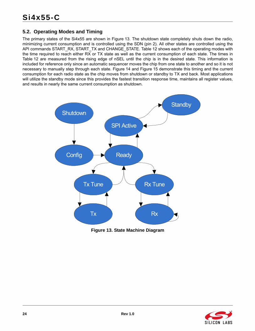
5.2. Operating Modes and TimingThe primary states of the Si4x55 are shown in Figure 13. The shutdown state completely shuts down the radio,minimizing current consumption and is controlled using the SDN (pin 2). All other states are controlled using theAPI commands START_RX, START_TX and CHANGE_STATE. Table 12 shows each of the operating modes withthe time required to reach either RX or TX state as well as the current consumption of each state. The times inTable 12 are measured from the rising edge of nSEL until the chip is in the desired state. This information isincluded for reference only since an automatic sequencer moves the chip from one state to another and so it is notnecessary to manually step through each state. Figure 14 and Figure 15 demonstrate this timing and the currentconsumption for each radio state as the chip moves from shutdown or standby to TX and back. Most applicationswill utilize the standby mode since this provides the fastest transition response time, maintains all register values,and results in nearly the same current consumption as shutdown.
Figure 13. State Machine Diagram
Shutdown
SPI Active
Standby
Ready
Tx Tune
Tx
Rx Tune
Rx
Config

Si4x55-C
Rev 1.0 25
Figure 14. Start-Up Timing and Current Consumption using Shutdown State
Table 12. Operating State Response Time and Current Consumption
State / Mode Response Time to Current in State / Mode
Tx Rx
Shutdown 30 ms 30 ms 30 nA
Standby 504 μs 516 μs 40 nA
SPI Active 288 μs 296 μs 1.5 mA
Ready 108 μs 120 μs 1.8 mA
Tx Tune 60 μs 6.8 mA
Rx Tune 84 μs 7.1 mA
Tx 132 μs 18 mA @ +10 dBm
Rx 120 μs 108 μs 10.9 mA
Shutdown = 30 nA
POWER_UP / CONFIG_SETUP = 29 ms@2 mA
Shutdown = 30 nA
Reg Inrush = 5 us@2 mA
POR = 1 [email protected] mA
Ready = 300 [email protected] mA
Tune = 100 [email protected] mA
Standby = 10 us@40 nA
TX = 19 mA

Si4x55-C
26 Rev 1.0
Figure 15. Start-Up Timing and Current Consumption using Standby State
5.2.1. Shutdown State
The shutdown state is the lowest current consumption state of the device and is entered by driving SDN (Pin 2)high. In this state, all register contents are lost and there is no SPI access. To exit this mode, drive SDN low. Thedevice will then initiate a power on reset (POR) along with internal calibrations. Once this POR period is complete,the POWER_UP command is required to initialize the radio and the configuration can then be loaded into thedevice. The SDN pin must be held high for at least 10 µs before driving it low again to insure the POR can beexecuted correctly. The shutdown state can be used to fully reset the part. If POR timing and voltage requirementscannot be met, it is highly recommended that SDN be controlled using the host processor rather than tying it toGND on the board.
5.2.2. Standby State
The standby state has similar current consumption to the shutdown state but retains all register values, allowing fora much faster response time. Because of these benefits, most applications will want to use standby mode ratherthan shutdown. The standby state is entered by using the CHANGE_STATE API command. While in this state, theSPI is accessible but any SPI event will automatically transition the chip to the SPI active state. After the SPI event,the host will need to re-command the device to standby mode.
5.2.3. SPI Active State
The SPI active state enables the device to process any SPI events, such as API commands. In this state, the SPIand boot up oscillator are enabled. The SPI active state is entered by using the CHANGE_STATE command orautomatically through an SPI event while in standby mode. If the SPI active state was entered automatically fromstandby mode, a CHANGE_STATE command will be needed to return the device to standby mode.
5.2.4. Ready State
Ready state is designed to give a fast transition time to TX or RX state with minimized current consumption. In thismode the crystal oscillator remains enabled to minimize the transition time. Ready state can be entered using theCHANGE_STATE command.
TX = 19 mA
Standby = 40 nA Standby = 40 nA
Reg Inrush = 5 us@2 mA
Ready = 300 [email protected] mA
Tune = [email protected] mA
Si4x55-C
Rev 1.0 27
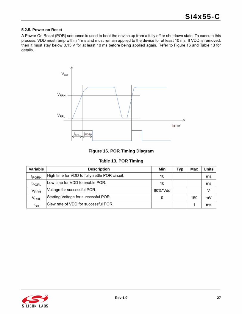
5.2.5. Power on Reset
A Power On Reset (POR) sequence is used to boot the device up from a fully off or shutdown state. To execute thisprocess, VDD must ramp within 1 ms and must remain applied to the device for at least 10 ms. If VDD is removed,then it must stay below 0.15 V for at least 10 ms before being applied again. Refer to Figure 16 and Table 13 fordetails.
Figure 16. POR Timing Diagram
Table 13. POR Timing
Variable Description Min Typ Max Units
tPORHHigh time for VDD to fully settle POR circuit. 10 ms
tPORLLow time for VDD to enable POR. 10 ms
VRRHVoltage for successful POR. 90%*Vdd V
VRRLStarting Voltage for successful POR. 0 150 mV
tSRSlew rate of VDD for successful POR. 1 ms

Si4x55-C
28 Rev 1.0
5.2.6. TX State
The TX state is used whenever the device is required to transmit data. It is entered using either the START_TX orCHANGE_STATE command. With the START_TX command, the next state can be defined to insure optimaltiming. When either command is sent to enter TX state, an internal sequencer automatically takes care of allactions required to move between states with no additional user commands needed. Examples of the timing of thistransition can be seen in Figure 14 and Figure 15. The specific sequencer controlled events that take place duringthis time can include enable internal LDOs, start up crystal oscillator, enable PLL, calibrate VCO/PLL, active poweramplifier, and transmit packet.
Figure 17 shows an example of the commands and timing for the START_TX command. CTS will go high as soonas the sequencer puts the part into TX state. As the sequencer is stepping through the events listed above, CTSwill be low and no new commands or property changes are allowed. If the nIRQ is used to monitor the currentstate, there will be a slight delay caused by the internal hardware from when the event actually occurs to when thetransition occurs on the nIRQ. The time from entering TX state to when the nIRQ will transition is 13 µs. If a GPIOis programmed for TX state or used as control for a transmit/receive switch (TR switch), there is no delay.
Figure 17. START_TX Commands and Timing
5.2.7. RX State
The RX state is used whenever the device is required to receive data. It is entered using either the START_RX orCHANGE_STATE commands. With the START_RX command, the next state can be defined to insure optimaltiming. When either command is sent to enter RX state, an internal sequencer automatically takes care of allactions required to move between states with no additional user commands needed. The sequencer controlledevents can include enable the digital and analog LDOs, start up the crystal oscillator, enable PLL, calibrate VCO,enable receiver circuits, and enable receive mode. The device will also automatically set up all receiver featuressuch as packet handling based upon the initial configuration of the device.
Initial State
Initial State
TX State TXCOMPLETE_STATE
TX State TXCOMPLETE_STATE
CTS
nSEL
SDI
Current State
FRR
nIRQ
GPIO-TX State
START_TX
Si4x55-C
Rev 1.0 29
5.3. InterruptsThe Si4x55 is capable of generating an interrupt signal when certain events occur. The chip notifies themicrocontroller that an interrupt event has occurred by setting the nIRQ output pin LOW = 0. This interrupt signalwill be generated when any one (or more) of the interrupt events occur. The nIRQ pin will remain low until themicrocontroller reads the Interrupt Status Registers. The nIRQ output signal will then be reset until the next changein status is detected.
The interrupt sources are grouped into three categories: packet handler, chip status, and modem. The individualinterrupts in these groups can be enabled/disabled in the interrupt property registers, 0x0101, 0x0102, and 0x0103.An interrupt must be enabled for it to trigger an event on the nIRQ pin. The interrupt group must be enabled as wellas the individual interrupts in API property 0x0100.
When an interrupt event occurs and the nIRQ pin is low, the interrupts are read and cleared using theGET_INT_STATUS command. By default all interrupts will be cleared once read. The instantaneous status of aspecific function may be read if the specific interrupt is enabled or disabled. The status results are provided afterthe interrupts and can be read with the same commands as the interrupts. The status bits will give the current stateof the function whether the interrupt is enabled or not. The following is a list of possible interrupts:
Chip status
Modem status
Packet handler status
Packet sent
Packet received
CRC error
Invalid preamble detected
Invalid sync detected
Preamble detected
Sync detected
State change
Command error
Chip ready
TX FIFO almost empty
RX FIFO almost full
RSSI interrupt
Si4x55-C
30 Rev 1.0
5.4. GPIOFour General Purpose IO (GPIO) pins are available for use in the application. The GPIOs are configured using theGPIO_PIN_CFG command. GPIO pins 0 and 1 should be used for active signals such as data or clock. GPIO pins2 and 3 have more susceptibility to generating spurious components in the synthesizer than pins 0 and 1. The drivestrength of the GPIO's can be adjusted with the GEN_CONFIG parameter in the GPIO_PIN_CFG command. Bydefault, the drive strength is set to the minimum. The default configuration and the state of the GPIO duringshutdown are shown in Table 14. For a complete list of the GPIO options, please refer to the EZRadio APIdocumentation zip file available from www.silabs.com.
Table 14. GPIOs
Pin SDN State POR Default
GPIO0 0 POR
GPIO1 0 CTS
GPIO2 0 POR
GPIO3 0 POR
nIRQ Resistive VDD pull-up nIRQ
SDO Resistive VDD pull-up SDO
SDI High Z SDI
SCLK High Z SCLK
NSEL High Z NSEL
Si4x55-C
Rev 1.0 31
6. Data Handling and Packet Handler
6.1. RX and TX FIFOsTwo 64-byte FIFOs are integrated into the chip, one for RX and one for TX. Writing to command register 66h loadsdata into the TX FIFO and reading from command register 77h reads data from the RX FIFO. For packet lengthsgreater than 64 bytes, RX_FIFO_ALMOST_FULL and TX_FIFO_ALMOST_EMPTY status bits and interrupts canbe used to manage the FIFO. The threshold value for these can be configured via the WDS radio configurationapplication GUI. The maximum payload length supported in packet handler mode is 255 bytes.
6.2. Packet HandlerThe Si4x55 includes integrated packet handler features such as preamble and sync word detection as well as CRCcalculation. This allows the chip to qualify and synchronize with legitimate transmissions independent of themicrocontroller. These features can be enabled using the RCA. In this setup, the preamble and sync word lengthcan be modified and the sync word pattern can be selected. If the preamble is greater than or equal to 4 bytes, thedevice uses the preamble detection circuit with a 2-byte detection threshold. If the preamble is less than 32 bits,then at least two bytes of sync word are required plus at least one byte of 0101 pattern (3 bytes total). In this case,preamble detection is skipped, and only sync word detection is used. For any combination of preamble and syncword less than three bytes, the device will use direct mode. The general packet structure is shown in Figure 18.
The EZConfig setup also provides the option to select a variable packet length. With this setting, the receiver is notrequired to know the packet length ahead of time. The transmitter sends the length of the packet immediately afterthe sync word. The packet structure for variable length packets is shown in Figure 19.
Figure 18. Packet Structure for Fixed Packet Length
Figure 19. Packet Structure for Variable Packet Length
6.3. Direct ModeIn direct mode, the packet handler (including FIFO) is bypassed, and the host MCU must feed the data stream tothe device in TX mode and read out the data stream in RX mode via GPIOs. The host MCU will process the dataand perform packet handler functions. This is commonly used to support legacy implementations where host MCUsoftware exists or to support non-standard packet structures. Some examples are packets with non 1010 preamblepattern, no preamble or sync word, or sync word with no edge transitions. WDS provides example projects tosupport both packet handler and direct modes.
Preamble Sync Word Data CRC0 – 255 Bytes 1 – 4 Bytes 1 – 255 Bytes 2 Bytes
Preamble Sync Word Length Data CRC0 – 255 Bytes 1 – 4 Bytes 1 Byte 1 – 255 Bytes 2 Bytes

Si4x55-C
32 Rev 1.0
7. Pin Descriptions
Pin Pin Name I/O Description
1 GND GND Ground
2 SDN IShutdown (0 – VDD V) – SDN=1, part will be in shutdown mode and contents of all registers are lost. SDN=0, all other modes
3 RXp ISi4455: Differential RF receiver inputSi4055: No ConnectSi4355: Differential RF receiver input
4 RXn ISi4455: Differential RF receiver inputSi4055: No ConnectSi4355: Differential RF receiver input
5 TX OSi4455: Transmit RF output Si4055: Transmit RF outputSi4355: No Connect
6 GND GND Ground
7 VDD VDD Supply voltage
8 VDD VDD Supply voltage
9 GND GND Ground
10 GPIO0 I/O General Purpose Digital I/O
11 GPIO1 I/O General Purpose Digital I/O
12 nIRQ OInterrupt Status Output – nIRQ = 0, interrupt event has occurred. Read interrupt status for event details
13 SCLK I Serial Clock Input (0 – VDD V): Provides serial data clock for 4-line serial data bus
14 SDO OSerial Data Output (0 – VDD V): Provides serial data readback function of internal control registers
15 SDI I Serial Data Input (0 – VDD V): Serial data stream input for 4-line serial data bus
16 nSEL ISerial Interface Select Input (0 – VDD V): Provides select/enable function for 4-line serial data bus
1
2
3
4
5
6 7 8 9 10
16
15
14
13
12
11
20 19 18 17GND
SDN
RXp
RXn
TX
GND
nSEL
SDI
SDO
SCLK
nIRQ
GPIO1V
DD
VD
D
GN
D
GP
IO0
GP
IO3
GP
IO2
XIN
XO
UT
Si4x55
Si4x55-C
Rev 1.0 33
17 XOUT O Crystal Oscillator Output
18 XIN ICrystal Oscillator Input: No dc bias required, but if used, should be set to 0.7 V. Also used for external TCXO input.
19 GPIO2 I/O General Purpose Digital I/O
20 GPIO3 I/O General Purpose Digital I/O
PKG PADDLE_GND GND
The exposed metal paddle on the bottom of the package supplies the RF and cir-cuit ground(s) for the entire chip. It is very important that a good solder connection is made between this exposed metal paddle and the ground plane of the underly-ing PCB.
Pin Pin Name I/O Description

Si4x55-C
34 Rev 1.0
8. Ordering Information
Part Number* Description Package Type Operating Temperature
Si4455-C2A-GM EZRadio Transceiver 3x3 QFN-20Pb-free
–40 to 85 °C
Si4355-C2A-GM EZRadio Receiver 3x3 QFN-20Pb-free
–40 to 85 °C
Si4055-C2A-GM EZRadio Transmitter 3x3 QFN-20Pb-free
–40 to 85 °C
*Note: Add an “R” at the end of the device part number to denote tape and reel option.

Si4x55-C
Rev 1.0 35
9. Package Outline
Figure 20. 20-pin QFN Package

Si4x55-C
36 Rev 1.0
Table 15. Package Diagram Dimensions
Dimension Min Nom Max
A 0.80 0.85 0.90
A1 0.00 0.035 0.05
A2 — 0.65 —
A3 0.203 REF
b 0.20 0.25 0.30
b1 0.25 0.30 0.35
D 3.00 BSC.
E 3.00 BSC.
e 0.50 BSC.
e1 0.515 BSC.
J 1.60 1.70 1.80
K 1.60 1.70 1.80
L 0.35 0.40 0.45
L1 0.25 0.30 0.35
aaa 0.10
bbb 0.10
ccc 0.08
ddd 0.10
eee 0.10
Notes:1. All dimensions shown are in millimeters (mm) unless otherwise noted.2. Dimensioning and Tolerancing per ANSI Y14.5M-1994.3. The drawing complies with JEDEC MO-220.4. Recommended card reflow profile is per the JEDEC/IPC J-STD-020 specification
for Small Body Components.

Si4x55-C
Rev 1.0 37
10. PCB Land Pattern
Figure 21. 20-pin QFN PCB Land Pattern
Table 16. PCB Land Pattern Dimensions
Dimension MIN MAX
C1 3.00
C2 3.00
E 0.50 REF
X1 0.25 0.35
X2 1.65 1.75
Y1 0.85 0.95
Y2 1.65 1.75
Y3 0.37 0.47
f 2.40 REF
c 0.25 0.35Note: All dimensions shown are in millimeters (mm) unless otherwise noted.

Si4x55-C
38 Rev 1.0
11. Top Marking
11.1. Si4x55 Top Marking
Figure 22. Si4x55 Top Marking
11.2. Top Marking Explanation
Mark Method: Laser
Line 1 Marking: Part Number 455A = Si4455-C2A055A = Si4055-C2A355A = Si4355-C2A
Firmware Revision A = C2A
Line 2 Marking: TTTT = Trace Code Internal tracking number
Line 3 Marking: Circle = 0.5 mm Diameter(Bottom-Left Justified)
Y = YearWW = Workweek
Assigned by the Assembly House. Corresponds to the last significant digit of the year and work week of the mold date.

DisclaimerSilicon Laboratories intends to provide customers with the latest, accurate, and in-depth documentation of all peripherals and modules available for system and software implementers using or intending to use the Silicon Laboratories products. Characterization data, available modules and peripherals, memory sizes and memory addresses refer to each specific device, and "Typical" parameters provided can and do vary in different applications. Application examples described herein are for illustrative purposes only. Silicon Laboratories reserves the right to make changes without further notice and limitation to product information, specifications, and descriptions herein, and does not give warranties as to the accuracy or completeness of the included information. Silicon Laboratories shall have no liability for the consequences of use of the information supplied herein. This document does not imply or express copyright licenses granted hereunder to design or fabricate any integrated circuits. The products must not be used within any Life Support System without the specific written consent of Silicon Laboratories. A "Life Support System" is any product or system intended to support or sustain life and/or health, which, if it fails, can be reasonably expected to result in significant personal injury or death. Silicon Laboratories products are generally not intended for military applications. Silicon Laboratories products shall under no circumstances be used in weapons of mass destruction including (but not limited to) nuclear, biological or chemical weapons, or missiles capable of delivering such weapons.
Trademark InformationSilicon Laboratories Inc., Silicon Laboratories, Silicon Labs, SiLabs and the Silicon Labs logo, CMEMS®, EFM, EFM32, EFR, Energy Micro, Energy Micro logo and combinations thereof, "the world’s most energy friendly microcontrollers", Ember®, EZLink®, EZMac®, EZRadio®, EZRadioPRO®, DSPLL®, ISOmodem ®, Precision32®, ProSLIC®, SiPHY®, USBXpress® and others are trademarks or registered trademarks of Silicon Laboratories Inc. ARM, CORTEX, Cortex-M3 and THUMB are trademarks or registered trademarks of ARM Holdings. Keil is a registered trademark of ARM Limited. All other products or brand names mentioned herein are trademarks of their respective holders.
http://www.silabs.com
Silicon Laboratories Inc.400 West Cesar ChavezAustin, TX 78701USA
Simplicity StudioOne-click access to MCU tools, documentation, software, source code libraries & more. Available for Windows, Mac and Linux!
www.silabs.com/simplicity
MCU Portfoliowww.silabs.com/mcu
SW/HWwww.silabs.com/simplicity
Qualitywww.silabs.com/quality
Support and Communitycommunity.silabs.com