Embed Size (px)
Citation preview

Rev. 2.02 8/05 Copyright © 2005 by Silicon Laboratories Si3034
Si3034
3.3 V GLOBAL DIRECT ACCESS ARRANGEMENT
Features
Complete DAA includes the following:
Applications
Description
The Si3034 is an integrated direct access arrangement (DAA) thatprovides a programmable line interface to meet global telephone lineinterface requirements. Available in two 16-pin small outline packages, iteliminates the need for an analog front end (AFE), isolation transformer,relays, opto-isolators, and 2- to 4-wire hybrid. The Si3034 dramaticallyreduces the number of discrete components and cost required to achievecompliance with global regulatory requirements. The Si3034 interfacesdirectly to standard modem DSPs.
Functional Block Diagram
Programmable line interface AC termination DC termination Ring detect threshold Ringer impedance
84 dB dynamic range TX/RX pathsIntegrated analog front end (AFE) and 2- to 4-wire hybridIntegrated ring detectorCaller ID supportLoop current monitor
Clock generationPulse dialing supportBilling tone detectionOverload detection3.3 or 5 V power supplyDirect interface to DSPsDaisy-chaining for up to eight devicesGreater than 3000 V isolationPatented isolation technologyLead-free/RoHS-compliant packages available
V.92 ModemsVoice Mail Systems
Set Top BoxesFax Machines
S i3 0 2 1 S i3 0 1 4
D ig i ta lIn te r fa c e
C o n tro lIn te r fa c e
Is o la t io nIn te r fa c e
H y b r ida n dD C
T e rm in a tio n
R in g D e te c t
O ff-H o o k
M C L K
S C L K
S D I
S D O
O F H K
M O D E
R E S E T
A O U T
F S Y N C
F C /R G D T
R X
F IL T
V R E GV R E G 2R E X TR E X T 2
R G D T /F S D
F IL T 2R E FD C T
R N G 1R N G 2Q BQ EQ E 2
Is o la tio nIn te r fa c e
US Patent # 5,870,046US Patent # 6,061,009Other Patents Pending
Ordering InformationSee page 61.
Pin Assignments
Si3021 (SOIC)
Si3021 (TSSOP)
Si3014 (SOIC or TSSOP)
1
2
3
4
5
6
7
8 9
1011
1213
16
1514
OFHKRGDT/FSDM0VA
GNDC1AM1AOUT
MCLKFSYNC
SCLKVD
SDOSDI
FC/RGDTRESET
1
2
3
4
5
6
7
8 9
1011
1213
16
1514
VD
SCLKFSYNCMCLKOFHKRGDT/FSDM0VA
SDOSDI
FC/RGDTRESETAOUT
M1C1AGND
1
2
3
4
5
6
7
8 9
1011
1213
16
1514
QE2DCT
IGNDC1B
RNG1RNG2
QBQE
FILT2FILTRXREXTREXT2REFVREG2VREG

Si3034
2 Rev. 2.02

Si3034
Rev. 2.02 3
TABLE OF CONTENTS
Section Page1. Electrical Specifications . . . . . . . . . . . . . . . . . . . . . . . . . . . . . . . . . . . . . . . . . . . . . . . . . . .42. Typical Application Schematic . . . . . . . . . . . . . . . . . . . . . . . . . . . . . . . . . . . . . . . . . . . . .153. Bill of Materials . . . . . . . . . . . . . . . . . . . . . . . . . . . . . . . . . . . . . . . . . . . . . . . . . . . . . . . . . .164. Analog Output . . . . . . . . . . . . . . . . . . . . . . . . . . . . . . . . . . . . . . . . . . . . . . . . . . . . . . . . . .185. Functional Description . . . . . . . . . . . . . . . . . . . . . . . . . . . . . . . . . . . . . . . . . . . . . . . . . . .19
5.1. Initialization . . . . . . . . . . . . . . . . . . . . . . . . . . . . . . . . . . . . . . . . . . . . . . . . . . . . . . . .215.2. On-Chip Charge Pump . . . . . . . . . . . . . . . . . . . . . . . . . . . . . . . . . . . . . . . . . . . . . . .215.3. Isolation Barrier . . . . . . . . . . . . . . . . . . . . . . . . . . . . . . . . . . . . . . . . . . . . . . . . . . . . .215.4. Off-Hook . . . . . . . . . . . . . . . . . . . . . . . . . . . . . . . . . . . . . . . . . . . . . . . . . . . . . . . . . .225.5. DC Termination . . . . . . . . . . . . . . . . . . . . . . . . . . . . . . . . . . . . . . . . . . . . . . . . . . . . .225.6. AC Termination . . . . . . . . . . . . . . . . . . . . . . . . . . . . . . . . . . . . . . . . . . . . . . . . . . . . .235.7. DC Termination Considerations . . . . . . . . . . . . . . . . . . . . . . . . . . . . . . . . . . . . . . . .235.8. Ring Detection . . . . . . . . . . . . . . . . . . . . . . . . . . . . . . . . . . . . . . . . . . . . . . . . . . . . . .235.9. Ringer Impedance . . . . . . . . . . . . . . . . . . . . . . . . . . . . . . . . . . . . . . . . . . . . . . . . . . .245.10. DTMF Dialing . . . . . . . . . . . . . . . . . . . . . . . . . . . . . . . . . . . . . . . . . . . . . . . . . . . . .245.11. Pulse Dialing . . . . . . . . . . . . . . . . . . . . . . . . . . . . . . . . . . . . . . . . . . . . . . . . . . . . . .245.12. Billing Tone Detection . . . . . . . . . . . . . . . . . . . . . . . . . . . . . . . . . . . . . . . . . . . . . . .255.13. Billing Tone Filter (Optional) . . . . . . . . . . . . . . . . . . . . . . . . . . . . . . . . . . . . . . . . . .255.14. On-Hook Line Monitor . . . . . . . . . . . . . . . . . . . . . . . . . . . . . . . . . . . . . . . . . . . . . . .265.15. Caller ID . . . . . . . . . . . . . . . . . . . . . . . . . . . . . . . . . . . . . . . . . . . . . . . . . . . . . . . . .265.16. Loop Current Monitor . . . . . . . . . . . . . . . . . . . . . . . . . . . . . . . . . . . . . . . . . . . . . . .265.17. Overload Detection . . . . . . . . . . . . . . . . . . . . . . . . . . . . . . . . . . . . . . . . . . . . . . . . .275.18. Analog Output . . . . . . . . . . . . . . . . . . . . . . . . . . . . . . . . . . . . . . . . . . . . . . . . . . . . .275.19. Gain Control . . . . . . . . . . . . . . . . . . . . . . . . . . . . . . . . . . . . . . . . . . . . . . . . . . . . . .275.20. Filter Selection . . . . . . . . . . . . . . . . . . . . . . . . . . . . . . . . . . . . . . . . . . . . . . . . . . . .275.21. Clock Generation Subsystem . . . . . . . . . . . . . . . . . . . . . . . . . . . . . . . . . . . . . . . . .275.22. Digital Interface . . . . . . . . . . . . . . . . . . . . . . . . . . . . . . . . . . . . . . . . . . . . . . . . . . . .295.23. Multiple Device Support . . . . . . . . . . . . . . . . . . . . . . . . . . . . . . . . . . . . . . . . . . . . .305.24. Power Management . . . . . . . . . . . . . . . . . . . . . . . . . . . . . . . . . . . . . . . . . . . . . . . .315.25. Calibration . . . . . . . . . . . . . . . . . . . . . . . . . . . . . . . . . . . . . . . . . . . . . . . . . . . . . . . .315.26. In-Circuit Testing . . . . . . . . . . . . . . . . . . . . . . . . . . . . . . . . . . . . . . . . . . . . . . . . . . .325.27. Exception Handling . . . . . . . . . . . . . . . . . . . . . . . . . . . . . . . . . . . . . . . . . . . . . . . . .325.28. Revision Identification . . . . . . . . . . . . . . . . . . . . . . . . . . . . . . . . . . . . . . . . . . . . . . .33
6. Control Registers . . . . . . . . . . . . . . . . . . . . . . . . . . . . . . . . . . . . . . . . . . . . . . . . . . . . . . . .41Appendix A—UL1950 3rd Edition . . . . . . . . . . . . . . . . . . . . . . . . . . . . . . . . . . . . . . . . . . . . .55Appendix B—CISPR22 Compliance . . . . . . . . . . . . . . . . . . . . . . . . . . . . . . . . . . . . . . . . . . .567. Pin Descriptions: Si3021 . . . . . . . . . . . . . . . . . . . . . . . . . . . . . . . . . . . . . . . . . . . . . . . . . .578. Pin Descriptions: Si3014 . . . . . . . . . . . . . . . . . . . . . . . . . . . . . . . . . . . . . . . . . . . . . . . . . .599. Ordering Guide1,2,3 . . . . . . . . . . . . . . . . . . . . . . . . . . . . . . . . . . . . . . . . . . . . . . . . . . . . . .6110. Package Outline: 16-Pin SOIC . . . . . . . . . . . . . . . . . . . . . . . . . . . . . . . . . . . . . . . . . . . . .6211. Package Outline: 16-Pin TSSOP . . . . . . . . . . . . . . . . . . . . . . . . . . . . . . . . . . . . . . . . . . .63Document Change List . . . . . . . . . . . . . . . . . . . . . . . . . . . . . . . . . . . . . . . . . . . . . . . . . . . . .64Contact Information . . . . . . . . . . . . . . . . . . . . . . . . . . . . . . . . . . . . . . . . . . . . . . . . . . . . . . . .66

Si3034
4 Rev. 2.02
1. Electrical Specifications
Table 1. Recommended Operating Conditions
Parameter1 Symbol Test Condition Min2 Typ Max2 Unit
Ambient Temperature TA F-Grade or K-Grade 0 25 70 °C
Si3021 Supply Voltage, Analog VA 4.75 5.0 5.25 V
Si3021 Supply Voltage, Digital3 VD 3.0 3.3/5.0 5.25 V
Notes:1. The Si3034 specifications are guaranteed when the typical application circuit (including component tolerance) and any
Si3021 and any Si3014 are used. See "2. Typical Application Schematic‚" on page 15.2. All minimum and maximum specifications are guaranteed and apply across the recommended operating conditions.
Typical values apply at nominal supply voltages and an operating temperature of 25 °C unless otherwise stated.3. The digital supply, VD, can operate from either 3.3 V or 5.0 V. The Si3021 supports interface to 3.3 V logic when
operating from 3.3 V and applies to both the serial port and the digital signals RGDT/FSD, OFHK, RESET, M0, and M1.

Si3034
Rev. 2.02 5
Figure 1. Test Circuit for Loop Characteristics
Table 2. Loop Characteristics(VD = 3.3 to 5.25 V, TA = 0 to 70 °C for F-Grade or K-Grade, See Figure 1)
Parameter Symbol Test Condition Min Typ Max UnitDC Termination Voltage VTR IL = 20 mA, ACT = 1
DCT = 11 (TBR21)— — 7.5 V
DC Termination Voltage VTR IL = 42 mA, ACT 1 DCT 11 (TBR21)
— — 14.5 V
DC Termination Voltage VTR IL = 50 mA, ACT = 1 DCT = 11 (TBR21)
— — 40 V
DC Termination Voltage VTR IL = 60 mA, ACT = 1 DCT = 11 (TBR21)
40 — — V
DC Termination Voltage VTR IL = 20 mA, ACT = 0 DCT = 01 (Japan)
— — 6.0 V
DC Termination Voltage VTR IL = 100 mA, ACT = 0 DCT = 01 (Japan)
11 — — V
DC Termination Voltage VTR IL = 20 mA, ACT = 0 DCT = 10 (FCC)
— — 7.5 V
DC Termination Voltage VTR IL = 100 mA, ACT = 0 DCT = 10 (FCC)
12 — — V
On Hook Leakage Current ILK VTR = –48V — — 1 µAOperating Loop Current ILP FCC/Japan Modes 13 — 120 mAOperating Loop Current ILP TBR21 Mode 13 — 60 mADC Ring Current w/o Caller ID — — 20 µADC Ring Current with Caller ID — 450 — µARing Detect Voltage1 VRD RT = 0 11 — 22 VRMS
Ring Detect Voltage1 VRD RT = 1 17 — 33 VRMS
Ring Frequency FR 15 — 68 HzRinger Equivalence Number2 REN w/o Caller ID — — 0.2Ringer Equivalence Number2 REN with Caller ID — 0.8 —Notes:
1. The ring signal is guaranteed to not be detected below the minimum. The ring signal is guaranteed to be detected above the maximum.
2. C15, R14, Z2, and Z3 not installed. See "5.9. Ringer Impedance‚" on page 24.
TIP
RING
+
–
Si3014 VTR
600 Ω
10 µF
IL

Si3034
6 Rev. 2.02
Table 3. DC Characteristics, VD = 5 V(VD = 4.75 to 5.25 V, TA = 0 to 70 °C for F-Grade or K-Grade)
Parameter Symbol Test Condition Min Typ Max Unit
High Level Input Voltage VIH 3.5 — — V
Low Level Input Voltage VIL — — 0.8 V
High Level Output Voltage VOH IO = –2 mA 3.5 — — V
Low Level Output Voltage VOL IO = 2 mA — — 0.4 V
Input Leakage Current IL –10 — 10 µA
Power Supply Current, Analog IA VA pin — 0.3 1 mA
Power Supply Current, Digital1 ID VD pin — 14 18 mA
Total Supply Current, Sleep Mode1 IA + ID PDN = 1, PDL = 0 — 1.3 2.5 mA
Total Supply Current, Deep Sleep1,2 IA + ID PDN = 1, PDL = 1 — .04 0.5 mA
Notes:1. All inputs at 0.4 or VD – 0.4 (CMOS levels). All inputs held static except clock and all outputs unloaded
(Static IOUT = 0 mA).2. RGDT is not functional in this state.
Table 4. DC Characteristics, VD = 3.3 V(VD = 3.0 to 3.6 V, TA = 0 to 70 °C for F-Grade or K-Grade)
Parameter Symbol Test Condition Min Typ Max Unit
High Level Input Voltage VIH 2.0 — — V
Low Level Input Voltage VIL — — 0.8 V
High Level Output Voltage VOH IO = –2 mA 2.4 — — V
Low Level Output Voltage VOL IO = 2 mA — — 0.35 V
Input Leakage Current IL –10 — 10 µA
Power Supply Current, Analog1,2 IA VA pin — 0.3 1 mA
Power Supply Current, Digital3 ID VD pin — 9 12 mA
Total Supply Current, Sleep Mode3 IA + ID PDN = 1, PDL = 0 — 1.2 2.5 mA
Total Supply Current, Deep Sleep3,4 IA + ID PDN = 1, PDL = 1 — .04 0.5 mA
Power Supply Voltage, Analog1,5 VA Charge Pump On 4.3 4.6 5.0 V
Notes:1. Only a decoupling capacitor should be connected to VA when the charge pump is on.2. There is no IA current consumption when the internal charge pump is enabled and only a decoupling capacitor is
connected to the VA pin.3. All inputs at 0.4 or VD – 0.4 (CMOS levels). All inputs held static except clock and all outputs unloaded
(Static IOUT = 0 mA).4. RGDT is not functional in this state.5. The charge pump is recommended to be used only when VD < 4.5 V. When the charge pump is not used, VA should be
applied to the device before VD is applied on power up if driven from separate supplies.

Si3034
Rev. 2.02 7
Table 5. AC Characteristics (VD = 3.0 to 5.25 V, TA = 0 to 70 °C for F-Grade or K-Grade, see 16 on page 15)
Parameter Symbol Test Condition Min Typ Max Unit
Sample Rate1 Fs Fs = FPLL2/5120 7.2 — 11.025 KHz
PLL1 Output Clock Frequency1 FPLL1 FPLL1 = FMCLK M1/N1 36 — 58 MHz
Transmit Frequency Response Low –3 dBFS Corner — 0 — Hz
Receive Frequency Response Low –3 dBFS Corner — 5 — Hz
Transmit Full Scale Level2 VFS — 1 — VPEAK
Receive Full Scale Level2,3 VFS — 1 — VPEAK
Dynamic Range4 DR ACT = 0, DCT = 10 (FCC)IL = 100 mA
— 82 — dB
Dynamic Range4 DR ACT = 0, DCT = 01 (Japan)IL = 20 mA
— 83 — dB
Dynamic Range4 DR ACT = 1, DCT = 11(TBR21)IL = 60 mA
— 84 — dB
Transmit Total Harmonic Distortion5 THD ACT = 0, DCT = 10 (FCC)IL = 100 mA
— –85 — dB
Transmit Total Harmonic Distortion5 THD ACT = 0, DCT = 01 (Japan)IL = 20 mA
— –76 — dB
Receive Total Harmonic Distortion5 THD ACT = 0, DCT = 01 (Japan)IL = 20 mA
— –74 — dB
Receive Total Harmonic Distortion5 THD ACT = 1, DCT = 11 (TBR21)IL = 60 mA
— –82 — dB
Dynamic Range (call progress AOUT) DRAO VIN = 1 kHz 60 — — dB
THD (call progress AOUT) THDAO VIN = 1 kHz — 1.0 — %
AOUT Full Scale Level — 0.75 VD — VPP
AOUT Output Impedance — 10 — kΩ
Mute Level (call progress AOUT) –90 — — dBFS
Dynamic Range (caller ID mode) DRCID VIN = 1 kHz, –13 dBFS — 60 — dB
Caller ID Full Scale Level (0 dB gain) VCID — 0.8 — VPEAK
Notes:1. See 23 on page 28.2. Measured at TIP and RING with 600 Ω termination at 1 kHz, as shown in Figure 1.3. Receive full scale level will produce –0.9 dBFS at SDO.4. DR = 20 log |Vin| + 20 log (RMS signal/RMS noise). Measurement is 300 to 3400 Hz. Applies to both transmit and
receive paths. Vin = 1 KHz, –3 dBFS, Fs = 10300 Hz.5. THD = 20 log (RMS distortion/RMS signal). Vin = 1 kHz, –3 dBFS, Fs = 10300 Hz.

Si3034
8 Rev. 2.02
Figure 2. General Inputs Timing Diagram
Table 6. Absolute Maximum Ratings
Parameter Symbol Value Unit
DC Supply Voltage VD –0.5 to 6.0 V
Input Current, Si3021 Digital Input Pins IIN ±10 mA
Digital Input Voltage VIND –0.3 to (VD + 0.3) V
Operating Temperature Range TA –40 to 100 °C
Storage Temperature Range TSTG –65 to 150 °C
Note: Permanent device damage may occur if the absolute maximum ratings are exceeded. Functional operation should be restricted to the conditions as specified in the operational sections of this data sheet. Exposure to absolute maximum rating conditions for extended periods may affect device reliability.
Table 7. Switching Characteristics—General Inputs(VD = 3.0 to 5.25 V, TA = 70 °C for F-Grade or K-Grade, CL = 20 pF)
Parameter1 Symbol Min Typ Max Unit
Cycle Time, MCLK tmc 16.67 — 1000 ns
MCLK Duty Cycle tdty 40 50 60 %
Rise Time, MCLK tr — — 5 ns
Fall Time, MCLK tf — — 5 ns
MCLK Before RESET ↑ tmr 10 — — cycles
RESET Pulse Width2 trl 250 — — ns
M0, M1 Before RESET↑3 tmxr 20 — — ns
Notes:1. All timing (except Rise and Fall time) is referenced to the 50% level of the waveform. Input test levels are
VIH = VD – 0.4 V, VIL = 0.4 V. Rise and Fall times are referenced to the 20% and 80% levels of the waveform.2. The minimum RESET pulse width is the greater of 250 ns or 10 MCLK cycle times.3. M0 and M1 are typically connected to VD or GND and should not be changed during normal operation.
MCLK
M0, M1
tr
RESET
tmc
tmr
tf
tmxr
VIH
VIL
trl

Si3034
Rev. 2.02 9
Figure 3. Serial Interface Timing Diagram (DCE = 0)
Table 8. Switching Characteristics—Serial Interface (DCE = 0)(VD = 3.0 to 5.25 V, TA = 70 °C for F-Grade or K-Grade, CL = 20 pF)
Parameter Symbol Min Typ Max Unit
Cycle time, SCLK tc 354 1/256 Fs — ns
SCLK duty cycle tdty — 50 — %
Delay time, SCLK ↑ to FSYNC ↓ td1 — — 10 ns
Delay time, SCLK ↑ to SDO valid td2 — — 20 ns
Delay time, SCLK ↑ to FSYNC ↑ td3 — — 10 ns
Setup time, SDI before SCLK ↓ tsu 25 — — ns
Hold time, SDI after SCLK ↓ th 20 — — ns
Setup time, FC ↑ before SCLK ↑ tsfc 40 — — ns
Hold time, FC ↑ after SCLK ↑ thfc 40 — — ns
Note: All timing is referenced to the 50% level of the waveform. Input test levels are VIH = VD – 0.4 V, VIL = 0.4 V.
SCLKtc
td1
VOH
VOL
FSYNC(mode 0)
FSYNC(mode 1)
td3
td3
td216 BitSDO
16 BitSDI
D15 D14 D1 D0
D0D1 D14D15
tsu th
tsfc thfc
FC

Si3034
10 Rev. 2.02
Figure 4. Serial Interface Timing Diagram (DCE = 1, FSD = 0)
Table 9. Switching Characteristics—Serial Interface (DCE = 1, FSD = 0)(VA = Charge Pump, VD = 3.0 to 5.25 V, TA = 0 to 70 °C for F-Grade or K-Grade, CL = 20 pF)
Parameter1,2 Symbol Min Typ Max Unit
Cycle Time, SCLK tc 354 1/256 Fs — nsSCLK Duty Cycle tdty — 50 — %Delay Time, SCLK ↑ to FSYNC ↑ td1 — — 10 nsDelay Time, SCLK ↑ to FSYNC ↓ td2 — — 10 nsDelay Time, SCLK ↑ to SDO valid td3 0.25tc – 20 — 0.25tc + 20 nsDelay Time, SCLK ↑ to SDO Hi-Z td4 — — 20 nsDelay Time, SCLK ↑ to RGDT ↓ td5 — — 20 nsDelay Time, SCLK ↑ to RGDT ↑ td6 — — 20 nsSetup Time, SDO Before SCLK ↓ tsu 25 — — nsHold Time, SDO After SCLK ↓ th 20 — — nsSetup Time, SDI Before SCLK tsu2 25 — — nsHold Time, SDI After SCLK th2 20 — — nsNotes:
1. All timing is referenced to the 50% level of the waveform. Input test levels are VIH = VD – 0.4 V, VIL = 0.4 V.2. Refer to the section "5.23. Multiple Device Support‚" on page 30 for functional details.
SCLK
FSYNC(mode 1)
tc
td1 td2 td2
FSYNC(mode 0)
td5 td6 td5
SDO(master)
FSD(Mode 0)
SDO(slave 1)
td3
D15 D14 D13 D0
tsu th td4
td3
D15
td5
SDI D15 D0D14
th2tsu2
td2FSD(Mode 1)
32 SCLKs
16 SCLKs 16 SCLKs
D13

Si3034
Rev. 2.02 11
Figure 5. Serial Interface Timing Diagram (DCE = 1, FSD = 1)
Table 10. Switching Characteristics—Serial Interface (DCE = 1, FSD = 1)(VD = 3.0 to 5.25 V, TA = 70 °C for F-Grade or K-Grade, CL = 20 pF)
Parameter Symbol Min Typ Max Unit
Cycle Time, SCLK tc 354 1/256 Fs — ns
SCLK Duty Cycle tdty — 50 — %
Delay Time, SCLK ↑ to FSYNC ↑ td1 — — 10 ns
Delay Time, SCLK ↑ to FSYNC ↓ td2 — — 10 ns
Delay Time, SCLK ↑ to SDO valid td3 0.25tc – 20 — 0.25tc + 20 ns
Delay Time, SCLK ↑ to SDO Hi-Z td4 — — 20 ns
Delay Time, SCLK ↑ to RGDT ↓ td5 — — 20 ns
Setup Time, SDO Before SCLK ↓ tsu 25 — — ns
Hold Time, SDO After SCLK ↓ th 20 — — ns
Setup Time, SDI Before SCLK tsu2 25 — — ns
Hold Time, SDI After SCLK th2 20 — — ns
Notes:1. All timing is referenced to the 50% level of the waveform. Input test levels are VIH = VD – 0.4 V, VIL = 0.4 V.2. Refer to "5.23. Multiple Device Support‚" on page 30 for functional details.
D15 D1 D0
SCLK
FSYNC(mode 1)
SDO(master)
FSD
SDI
tc
SDO(slave 1)
td1
D14
td2
td3
D15 D14 D13 D0
tsu th td4
td3
D15
td5
th2tsu2

Si3034
12 Rev. 2.02
Table 11. Digital FIR Filter Characteristics—Transmit and Receive(VD = 3.0 to 5.25 V, Sample Rate = 8 kHz, TA = 70 °C for F-Grade or K-Grade)
Parameter Symbol Min Typ Max Unit
Passband (0.1 dB) F(0.1 dB) 0 — 3.3 kHz
Passband (3 dB) F(3 dB) 0 — 3.6 kHz
Passband Ripple Peak-to-Peak –0.1 — 0.1 dB
Stopband — 4.4 — kHz
Stopband Attenuation –74 — — dB
Group Delay tgd — 12/Fs — secNote: Typical FIR filter characteristics for Fs = 8000 Hz are shown in Figures 6, 7, 8, and 9.
Table 12. Digital IIR Filter Characteristics—Transmit and Receive(VD = 3.0 to 5.25 V, Sample Rate = 8 kHz, TA = 70 °C for F-Grade or K-Grade)
Parameter Symbol Min Typ Max Unit
Passband (3 dB) F(3 dB) 0 — 3.6 kHz
Passband Ripple Peak-to-Peak –0.2 — 0.2 dB
Stopband — 4.4 — kHz
Stopband Attenuation –40 — — dB
Group Delay tgd — 1.6/Fs — secNote: Typical IIR filter characteristics for Fs = 8000 Hz are shown in Figures 10, 11, 12, and 13. Figures 14 and 15 show
group delay versus input frequency.
Si3034
Rev. 2.02 13
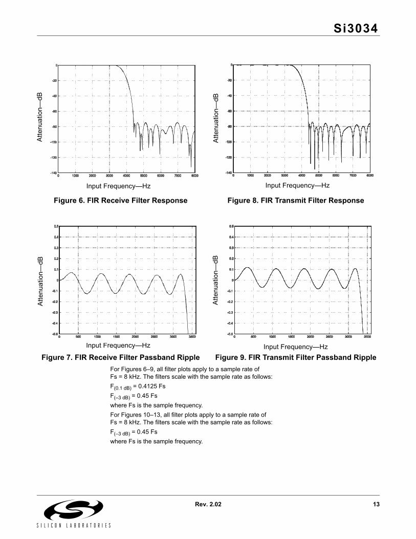
Figure 6. FIR Receive Filter Response
Figure 7. FIR Receive Filter Passband Ripple
Figure 8. FIR Transmit Filter Response
Figure 9. FIR Transmit Filter Passband RippleFor Figures 6–9, all filter plots apply to a sample rate of Fs = 8 kHz. The filters scale with the sample rate as follows:F(0.1 dB) = 0.4125 FsF(–3 dB) = 0.45 Fswhere Fs is the sample frequency.For Figures 10–13, all filter plots apply to a sample rate of Fs = 8 kHz. The filters scale with the sample rate as follows:F(–3 dB) = 0.45 Fswhere Fs is the sample frequency.
Input Frequency—Hz
Atte
nuat
ion—
dB
Input Frequency—Hz
Atte
nuat
ion—
dB
Atte
nuat
ion—
dB
Input Frequency—Hz
Input Frequency—Hz
Atte
nuat
ion—
dB

Si3034
14 Rev. 2.02
Figure 10. IIR Receive Filter Response
Figure 11. IIR Receive Filter Passband Ripple
Figure 12. IIR Transmit Filter Response
Figure 13. IIR Transmit Filter Passband Ripple
Figure 14. IIR Receive Group Delay
Figure 15. IIR Transmit Group Delay
Input Frequency (Hz)
Atte
nuat
ion—
dB
Input Frequency (Hz)
Atte
nuat
ion—
dB
Input Frequency (Hz)
Atte
nuat
ion—
dB
Input Frequency (Hz)
Atte
nuat
ion—
dB
Input Frequency (Hz)
Del
ay—
µs
Input Frequency (Hz)
Del
ay—
µs

Si3034
Rev. 2.02 15
2. Typical Application Schematic
R19
C2
5
+C
14
R15
R17
U2
Si3
01
2/4
1 2 3 4 5 6 7 891
0111
21
31
41
51
6T
STA
/QE
2T
ST
B/D
CT
IGN
DC
1B
RN
G1
RN
G2
QB
QE
VR
EG
NC
/VR
EG
2N
C/R
EF
DC
T/R
EX
T2
RE
XT
RX
NC
/FIL
TT
X/F
ILT
2
R2
1
R2
8
+C
23
M0
L1
Decouplin
gcap
for
U1
VD
R1
0
Note
1:T
his
desig
nta
rgets
two
basic
build
s:
-A
nF
CC
and
JA
TE
com
plia
nt
desig
nusin
gth
eS
i3035
chip
set.
-A
worldw
ide
desig
nusin
gth
eS
i3034
chip
set.
R6
C7
Z5
RG
DT
b
C4
C1
9
C2
4
C2
Note
3:S
ee
"Bill
ing
Tone
Dete
ction"
section
for
optionalbill
ing
tone
filter
(Germ
any,
Sw
itzerland,
South
Afr
ica).
R1
8
Note
5:F
or
Si3
035
desig
ns
R29
ispopula
ted
with
a0
oh
mre
sis
tor
and
R30
isnotin
sta
lled.F
or
Si3
034
desig
ns
R29
isnotin
sta
lled
and
R30
ispopula
ted
with
a0
oh
mre
sis
tor.
D1
C1
8
MC
LK
R5
D2
R8
+C
12
Decouplin
gcap
for
U1
VA
SD
O
Q1
C8
L2
R2
9
C1
0
R1
3
R2
2R
9
Q2
TIP
FB
1
VC
C
D3
BA
V9
9
+
C5
R2
7
SD
I
Q3
C9
Z1
SOIC
Pinout
R2
3C
29
C6
Z4
C1
C3
2
FC
SC
LK
C3
0
R1
2
AO
UT
C1
3
C1
6
D4
BA
V9
9M
1
RE
SE
Tb
R16
R3
0
C2
0
See
Note
6N
ote
2:R
12,R
13
and
C14
are
only
required
ifcom
ple
xA
Cte
rmin
ation
isused
(AC
Tbit
=1).
RV
2
C3
RV
1
R11
C11
See
Note
5
R3
10
R4
R2
4
C2
8
U1
Si3
02
1
1 2 3 4 5 6 7 891
011
12
13
14
15
16
MC
LK
FS
YN
CS
CL
KV
DS
DO
SD
IF
CR
ES
ET
AO
UT
M1
C1
AG
ND
VA
M0
RG
DT
OF
HK
FB
2
Note
4:S
ee
Appendix
for
applic
ations
requirin
gU
L1950
3rd
ed
itio
nco
mp
lian
ce
.
C2
2
RIN
G
R2
Q4
Note
6:P
lease
refe
rto
Appendix
Bfo
rin
form
ation
regard
ing
L1
and
L2.
R7
C3
1
No
Gro
un
dP
lan
eIn
DA
AS
ectio
n
OF
HK
bR
1
FS
YN
Cb
Figu
re16
.Typ
ical
App
licat
ion
Circ
uit f
or th
e D
ual D
esig
n Si
3034
and
Si3
035

Si3034
16 Rev. 2.02
3. Bill of MaterialsTable 13. Global Component Values
Component1 Value Supplier(s)
C1,C42 150 pF, 3 kV, X7R,±20% Novacap, Venkel, Johanson, Murata, Panasonic
C2,C11,C23,C28,C29,C31,C32 Not Installed
C3 0.22 µF, 16 V, X7R,±20% Novacap, Venkel, Johanson, Murata, Panasonic
C5 0.1 µF, 50 V, X7R/Elec/Tant, ±20%
C6,C10,C16 0.1 µF, 16 V, X7R, ±20%
C7,C8 560 pF, 250 V, X7R, ±20% Novacap, Johanson, Murata, Panasonic
C9 10 nF, 250 V, X7R, ±20%
C12 0.22 µF, 16 V, Tant, ±20% Panasonic
C13 0.47 µF, 16 V, X7R, ±20%
C14 0.68 µF, 16 V, X7R/Elec/Tant, ±20%
C18,C19 3.9 nF, 16 V, X7R, ±20%
C20 0.01 µF, 16 V, X7R, ±20%
C22 1800 pF, 50 V, X7R, ±20%
C24,C252 1000 pF, 3 kV, X7R, ±10%
C303 Not InstalledD1,D24 Dual Diode, 300 V, 225 mA Central Semiconductor
D3,D4 BAV99 Dual Diode, 70 V, 350 mW Diodes, Inc., OnSemiconductor, Fairchild
FB1,FB2 Ferrite Bead Murata
L1,L25 330 µH, DCR <3 Ω, 120 mA, ±10% Taiyo Yuden, ACT, Transtek Magnetics, Cooper Electronics
Q1,Q3 A42, NPN, 300 V OnSemiconductor, Fairchild
Q2 A92, PNP, 300 V OnSemiconductor, Fairchild
Q46 BCP56T1, NPN, 60 V, 1/2 W OnSemiconductor, Fairchild
RV1 Sidactor, 275 V, 100 A Teccor, ST Microelectronics, Microsemi, TI
RV27 Not Installed
R1,R4,R21,R22,R23 Not Installed
R2 402 Ω, 1/16 W, ±1%
R38 Not Installed
R5 36 kΩ, 1/16 W, ±5%
R6 120 kΩ, 1/16 W, ±5%
R7,R8,R15,R16,R17,R199 4.87 kΩ, 1/4 W, ±1%
R9,R10 56 kΩ, 1/10 W, ±5%
R11 10 kΩ, 1/16 W, ±1%
R12 78.7 Ω, 1/16 W, ±1%
R13 215 Ω, 1/16 W, ±1%
R18 2.2 kΩ, 1/10 W, ±5%
R24 150 Ω, 1/16 W, ±5%
R27,R28 10 Ω, 1/10 W, ±5%
R29 Not Installed
R30 0 Ω, 1/10 W
U1 Si3021 Silicon Labs
U2 Si3014 Silicon Labs
Z1 Zener Diode, 43 V, 1/2 W Vishay, OnSemiconductor, Rohm
Z4,Z5 Zener Diode, 5.6 V, 1/2 W Diodes, Inc., OnSemiconductor, Fairchild
Notes:1. The following reference designators were intentionally omitted: C15, C17, C21, C26, C27, R14, and R20.2. X2/Y3 or Y2 class capacitors are used to comply with the Nordic requirements of EN60950 and may also be used to achieve higher surge immunity.3. Install only if needed for improved radiated emissions performance (10 pF, 16 V, NPO, ±10%).4. Several diode bridge configurations are acceptable (suppliers include General Semi., Diodes Inc.)5. See Appendix B for additional considerations.6. Q4 may require copper on board to meet 1/2 power requirement. (Contact transistor manufacturer for details.)7. RV2 can be installed to improve performance from 2500 V to 3500 V for multiple longitudinal surges (270 V, MOV).8. If the charge pump is not enabled (with the CPE bit in Register 6), VA must be 4.75 to 5.25 V. R3 can be installed with a 10 Ω, 1/10 W, ±5% if VD is also
4.75 to 5.25 V.9. The R7, R8, R15 and R16, R17, R19 resistors may each be replaced with a single resistor of 1.62 kΩ, 3/4 W, ±1%.

Si3034
Rev. 2.02 17
Table 14. FCC Component Values—Si3035 Chipset
Component1 Value Supplier(s)C1,C42 150 pF, 3 kV, X7R,±20% Novacap, Venkel, Johanson, Murata, Panasonic
C2 Not InstalledC3 0.22 µF, 16 V, X7R, ±20%C5 1.0 µF, 16 V, Elec/Tant, ±20%
C6,C10,C16 0.1 µF, 16 V, X7R, ±20%C9,C28,C29 15 nF, 250 V, X7R, ±20% Novacap, Johanson, Murata, Panasonic
C11 39 nF, 16 V, X7R, ±20%C7,C8,C12,C13,C14
C18,C19,C20,C22,C233Not Installed
C24,C25,C31,C322,4 1000 pF, 3 kV, X7R, ±10% Novacap, Venkel, Johanson, Murata, Panasonic
C305 Not InstalledD1,D26 Dual Diode, 300 V, 225 mA Central SemiconductorD3,D4 BAV99 Dual Diode, 70 V, 350 mW Diodes, Inc., OnSemiconductor, Fairchild
FB1,FB2 Ferrite Bead MurataL1,L2 0 Ω, 1/10 WQ1,Q3 A42, NPN, 300 V OnSemiconductor, Fairchild
Q2 A92, PNP, 300 V OnSemiconductor, FairchildQ4 Not Installed
RV1 Sidactor, 275 V, 100 A Teccor, ST Microelectronics, Microsemi, TIRV2 240 V, MOV PanasonicR1 51 Ω, 1/2 W, ±5%R2 15 Ω, 1/4 W, ±5%R37 Not Installed
R4,R18,R21 301 Ω, 1/10 W, ±1%R5,R6 36 kΩ, 1/10 W, ±5%
R7,R8,R113,R12,R13,R15R16,R17,R19,R24 Not Installed
R9,R10 2 kΩ, 1/10 W, ±5%R22,R23 20 kΩ, 1/10 W, ±5%R27,R28 10 Ω, 1/10 W, ±5%
R29 0 Ω, 1/10 WR30 Not InstalledU1 Si3021 Silicon LabsU2 Si3012 Silicon LabsZ1 Zener Diode, 18 V Vishay, OnSemiconductor, Rohm
Z4,Z5 Zener Diode, 5.6 V, 1/2 W Diodes, Inc., OnSemiconductor, FairchildNotes:
1. The following reference designators were intentionally omitted: C15, C17, C21, C26, C27, R14, and R20.2. X2/Y3 or Y2 class capacitors may also be used to achieve surge performance of 5 kV or better.3. If JATE support is required using the Si3035 chipset, C23 should be populated with a 0.1 µF, 16 V, Tant/Elec/X7R,
±20%, and R11 should be populated with a 2.7 nF, 16 V, X7R, ±20% capacitor.4. Alternate population option is C24, C25 (2200 pF, 3 kV, X7R, ±10% and C31, C32 not installed).5. Install only if needed for improved radiated emissions performance (10 pF, 16 V, NPO, ±10%).6. Several diode bridge configurations are acceptable (suppliers include General Semi., Diodes Inc.).7. If the charge pump is not enabled (with the CPE bit in Register 6), VA must be 4.75 to 5.25 V. R3 can be installed with a
10 Ω, 1/10 W, ±5% if VD is also 4.75 to 5.25 V.

Si3034
18 Rev. 2.02
4. Analog OutputFigure 17 illustrates an optional application circuit to support the analog output capability of the Si3034 for callprogress monitoring purposes. The ARM bits in Register 6 allow the receive path to be attenuated by 0 dB, –6 dB,or –12 dB. The ATM bits, which are also in Register 6, allow the transmit path to be attenuated by –20 dB, –26 dB,or –32 dB. Both the transmit and receive paths can also be independently muted.
Figure 17. Optional Connection to AOUT for a Call Progress Speaker
‘Table 15. Component Values—Optional Connection to AOUT
Symbol Value
C1 2200 pF, 16 V, ±20%
C2, C3, C5 0.1 µF, 16 V, ±20%
C4 100 µF, 16 V, Elec. ±20%
C6 820 pF, 16 V, ±20%
R1 10 kΩ, 1/10 W, ±5%
R2 10 Ω, 1/10 W, ±5%
R3 47 kΩ, 1/10 W, ±5%
U1 LM386
AOUT
C1
C2
C6 R1
R3 C4
C3C5
R2Speaker
+–
+3
2
4
56
+5 V
Si3034
Rev. 2.02 19
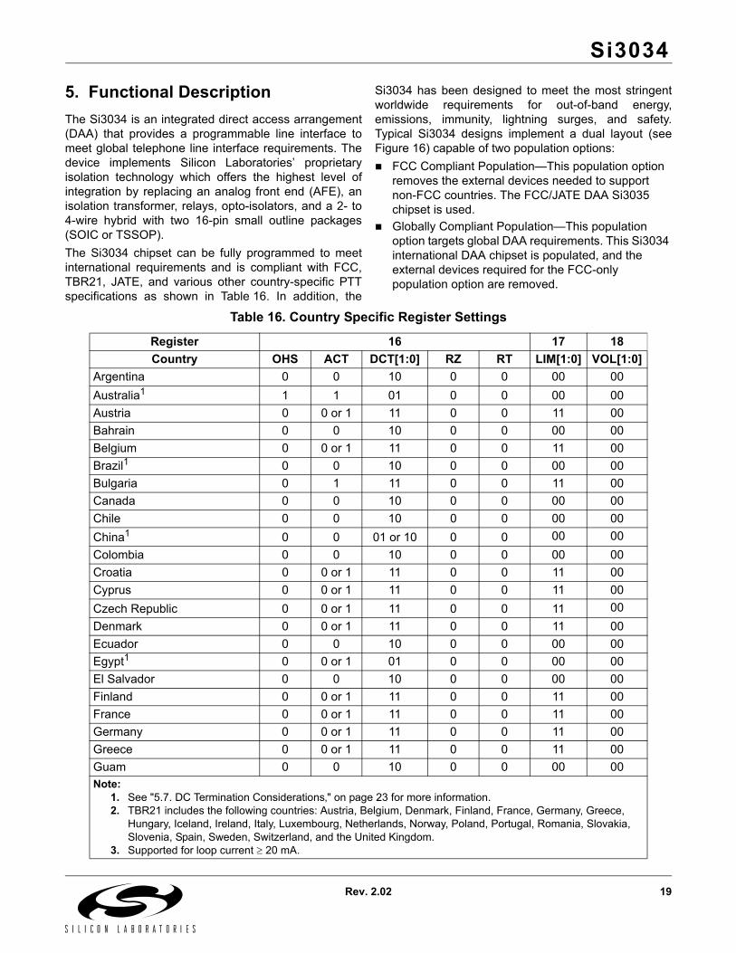
5. Functional DescriptionThe Si3034 is an integrated direct access arrangement(DAA) that provides a programmable line interface tomeet global telephone line interface requirements. Thedevice implements Silicon Laboratories’ proprietaryisolation technology which offers the highest level ofintegration by replacing an analog front end (AFE), anisolation transformer, relays, opto-isolators, and a 2- to4-wire hybrid with two 16-pin small outline packages(SOIC or TSSOP). The Si3034 chipset can be fully programmed to meetinternational requirements and is compliant with FCC,TBR21, JATE, and various other country-specific PTTspecifications as shown in Table 16. In addition, the
Si3034 has been designed to meet the most stringentworldwide requirements for out-of-band energy,emissions, immunity, lightning surges, and safety.Typical Si3034 designs implement a dual layout (seeFigure 16) capable of two population options:
FCC Compliant Population—This population option removes the external devices needed to support non-FCC countries. The FCC/JATE DAA Si3035 chipset is used.Globally Compliant Population—This population option targets global DAA requirements. This Si3034 international DAA chipset is populated, and the external devices required for the FCC-only population option are removed.
Table 16. Country Specific Register Settings
Register 16 17 18Country OHS ACT DCT[1:0] RZ RT LIM[1:0] VOL[1:0]
Argentina 0 0 10 0 0 00 00Australia1 1 1 01 0 0 00 00Austria 0 0 or 1 11 0 0 11 00Bahrain 0 0 10 0 0 00 00Belgium 0 0 or 1 11 0 0 11 00Brazil1 0 0 10 0 0 00 00Bulgaria 0 1 11 0 0 11 00Canada 0 0 10 0 0 00 00Chile 0 0 10 0 0 00 00China1 0 0 01 or 10 0 0 00 00Colombia 0 0 10 0 0 00 00Croatia 0 0 or 1 11 0 0 11 00Cyprus 0 0 or 1 11 0 0 11 00Czech Republic 0 0 or 1 11 0 0 11 00Denmark 0 0 or 1 11 0 0 11 00Ecuador 0 0 10 0 0 00 00Egypt1 0 0 or 1 01 0 0 00 00El Salvador 0 0 10 0 0 00 00Finland 0 0 or 1 11 0 0 11 00France 0 0 or 1 11 0 0 11 00Germany 0 0 or 1 11 0 0 11 00Greece 0 0 or 1 11 0 0 11 00Guam 0 0 10 0 0 00 00Note:
1. See "5.7. DC Termination Considerations‚" on page 23 for more information.2. TBR21 includes the following countries: Austria, Belgium, Denmark, Finland, France, Germany, Greece,
Hungary, Iceland, Ireland, Italy, Luxembourg, Netherlands, Norway, Poland, Portugal, Romania, Slovakia, Slovenia, Spain, Sweden, Switzerland, and the United Kingdom.
3. Supported for loop current ≥ 20 mA.

Si3034
20 Rev. 2.02
Hong Kong 0 0 10 0 0 00 00Hungary 0 0 or 1 11 0 0 11 00Iceland 0 0 or 1 11 0 0 11 00India 0 0 10 0 0 00 00Indonesia 0 0 10 0 0 00 00Ireland 0 0 or 1 11 0 0 11 00Israel 0 0 or 1 11 0 0 11 00Italy 0 0 or 1 11 0 0 11 00Japan1 0 0 01 0 0 00 00Jordan1 0 0 01 0 0 00 00Kazakhstan1 0 0 10 0 0 00 00Kuwait 0 0 10 0 0 00 00Latvia 0 0 or 1 11 0 0 11 00Lebanon 0 0 or 1 11 0 0 11 00Luxembourg 0 0 or 1 11 0 0 11 00Macao 0 0 10 0 0 00 00Malaysia1,3 0 0 01 0 0 00 00Malta 0 0 or 1 11 0 0 11 00Mexico 0 0 10 0 0 00 00Morocco 0 0 or 1 11 0 0 11 00Netherlands 0 0 or 1 11 0 0 11 00New Zealand 0 1 10 0 0 00 00Nigeria 0 0 or 1 11 0 0 11 00Norway 0 0 or 1 11 0 0 11 00Oman1 0 0 01 0 0 00 00Pakistan1 0 0 01 0 0 00 00Peru 0 0 10 0 0 00 00Philippines1 0 0 01 0 0 00 00
Poland 0 0 or 1 11 0 0 11 00Portugal 0 0 or 1 11 0 0 11 00Romania 0 0 or 1 11 0 0 11 00Russia1 0 0 10 0 0 00 00Saudi Arabia 0 0 10 0 0 00 00Singapore 0 0 10 0 0 00 00Slovakia 0 0 11 0 0 11 00Slovenia 0 0 11 0 0 11 00
Table 16. Country Specific Register Settings (Continued)
Register 16 17 18Country OHS ACT DCT[1:0] RZ RT LIM[1:0] VOL[1:0]
Note:1. See "5.7. DC Termination Considerations‚" on page 23 for more information.2. TBR21 includes the following countries: Austria, Belgium, Denmark, Finland, France, Germany, Greece,
Hungary, Iceland, Ireland, Italy, Luxembourg, Netherlands, Norway, Poland, Portugal, Romania, Slovakia, Slovenia, Spain, Sweden, Switzerland, and the United Kingdom.
3. Supported for loop current ≥ 20 mA.

Si3034
Rev. 2.02 21
5.1. InitializationWhen the Si3034 is initially powered up, the RESET pinshould be asserted. When the RESET pin isdeasserted, the registers will have default values. Thisreset condition guarantees the line-side chip (Si3014) ispowered down with no possibility of loading the line (i.e.,off-hook). An example initialization procedure is outlinedbelow:1. Program the PLLs with registers 7 to 9 (N1[7:0], M1[7:0],
N2[3:0], and M2[3:0]) to the appropriate divider ratios for the supplied MCLK frequency and desired sample rate, as defined in "5.21. Clock Generation Subsystem‚" on page 27.
2. Wait until the PLLs are locked. This time is between 100 µs and 1 ms.
3. Write an 80H into Register 6. This enables the charge pump for the VA pin, powers up the line-side chip (Si3014), and enables the AOUT for call progress monitoring.
4. Set the desired line interface parameters (i.e., DCT[1:0], ACT, OHS, RT, LIM[1:0], and VOL[1:0]) as defined by "Country Specific Register Settings" shown in Table 16.
After this procedure is complete, the Si3034 is ready forring detection and off-hook.
5.2. On-Chip Charge PumpThe Si3034 has an on-chip charge pump that canproduce the VA supply needed by the patentedcommunication link. This on-chip power supply can beenabled by setting bit 7 in Register 6 to 1.Before enabling the line-side chip, care should be takento ensure it is properly powered. If the on-chip chargepump is used to provide the VA supply, R3 should not bepopulated. If the on-chip charge pump is not used, theVA supply may be powered from the digital powersupply (VD). In this case, VD should be at least 4.75 V,and R3 should be populated. A separate 5 V powersupply may also be used for the VA supply, in whichcase, R3 should not be populated.
5.3. Isolation BarrierThe Si3034 achieves an isolation barrier through low-cost, high-voltage capacitors in conjunction with SiliconLaboratories’ proprietary signal processing techniques.These techniques eliminate any signal degradation dueto capacitor mismatches, common mode interference, ornoise coupling. As shown in 16 on page 15, the C1, C4,C24, and C25 capacitors isolate the Si3021 (DSP-side)from the Si3014 (line-side). All transmit, receive, control,ring detect, and caller ID data are communicated throughthis barrier. Y2 class capacitors may be used for theisolation barrier to achieve surge performance of 5 kV orgreater.
South Africa 1 0 10 1 0 00 00
South Korea 0 0 10 0 0 00 00Spain 0 0 or 1 11 0 0 11 00Sweden 0 0 or 1 11 0 0 11 00Switzerland 0 0 or 1 11 0 0 11 00Taiwan1 0 0 10 0 0 00 00TBR211,2 0 0 or 1 11 0 0 11 00Thailand1 0 0 01 0 0 00 00UAE 0 0 10 0 0 00 00United Kingdom 0 0 or 1 11 0 0 11 00USA 0 0 10 0 0 00 00Yemen 0 0 10 0 0 00 00
Table 16. Country Specific Register Settings (Continued)
Register 16 17 18Country OHS ACT DCT[1:0] RZ RT LIM[1:0] VOL[1:0]
Note:1. See "5.7. DC Termination Considerations‚" on page 23 for more information.2. TBR21 includes the following countries: Austria, Belgium, Denmark, Finland, France, Germany, Greece,
Hungary, Iceland, Ireland, Italy, Luxembourg, Netherlands, Norway, Poland, Portugal, Romania, Slovakia, Slovenia, Spain, Sweden, Switzerland, and the United Kingdom.
3. Supported for loop current ≥ 20 mA.

Si3034
22 Rev. 2.02
The proprietary communications link is disabled bydefault. To enable it, the PDL bit in Register 6 must becleared. No communication between the Si3021 andSi3014 can occur until this bit is cleared. The clockgenerator must be programmed to an acceptablesample rate prior to clearing the PDL bit.
5.4. Off-HookThe communication system generates an off-hookcommand by applying logic 0 to the OFHK pin or bysetting the OH bit in Register 5. The OFHK pin must beenabled by setting the OHE bit in Register 5. WithOFHK at logic 0, the system is in an off-hook state.The off-hook state is used to seize the line for incoming/outgoing calls and can also be used for pulse dialing.With OFHK at logic 1, negligible dc current flowsthrough the hookswitch. When a logic 0 is applied to theOFHK pin, the hookswitch transistor pair, Q1 & Q2, turnon. This applies a termination impedance across TIPand RING and causes dc loop current to flow. Thetermination impedance has both an ac and dccomponent.When executing an off-hook sequence, the Si3034requires 1548/Fs seconds to complete the off-hook andprovide phone-line data on the serial link. This includesthe 12/Fs filter group delay. If necessary, for the shortestdelay, a higher Fs may be established prior to executingthe off-hook, such as an Fs of 10.286 kHz. The delayallows for line transients to settle prior to normal use.
5.5. DC TerminationThe Si3034 has three programmable dc terminationmodes which are selected with the DCT[1:0] bits inRegister 16.Japan Mode (DCT[1:0] = 01 b), shown in Figure 18, is alower voltage mode and supports a transmit full scalelevel of –2.71 dBm. Higher transmit levels for DTMFdialing are also supported. See "5.10. DTMF Dialing‚"on page 24. The low-voltage requirement is dictated bycountries, such as Japan and Malaysia.
Figure 18. Japan Mode I/V CharacteristicsFCC Mode (DCT[1:0] = 10 b), shown in Figure 19, is thedefault dc termination mode and supports a transmit fullscale level of –1 dBm at TIP and RING. This modemeets FCC requirements in addition to the requirementsof many other countries.
Figure 19. FCC Mode I/V CharacteristicsTBR21 Mode (DCT[1:0] = 11 b), shown in Figure 20,provides current limiting, while maintaining a transmitfull scale level of –1 dBm at TIP and RING. In this mode,the dc termination will current limit before reaching60 mA.
Figure 20. TBR21 Mode I/V Characteristics
5.6. AC TerminationThe Si3034 has two ac termination impedancesselected with the ACT bit in Register 16.ACT = 0 is a real, nominal 600 Ω termination, whichsatisfies the impedance requirements of FCC part 68,JATE, and other countries. This real impedance is setby circuitry internal to the Si3034 as well as the resistor,
10.5109.5
98.5
8
7.57
6.5
.01 .02 .03 .04 .05 .06 .07 .08 .09 .1Loop Current (A)
Japan DCT Mode
Volta
ge A
cros
s D
AA (
V )
65.5
.11
12
11
10
9
8
7
6
FCC DCT Mode
.01 .02 .03 .04 .05 .06 .07 .08 .09 .1 .11Loop Current (A)
Volta
ge A
cros
s D
AA
( V
)
45
40
35
3025
2015
10
5.015 .02 .025 .03 .035 .04 .045 .05 .055 .06
Loop Current (A)
TBR21 DCT Mode
Volta
ge A
cros
s D
AA
( V
)

Si3034
Rev. 2.02 23
R2, connected to the REXT pin. ACT = 1 is a complex impedance which satisfies theimpedance requirements of Australia, New Zealand,South Africa, TBR21, and some European NET4countries such as the UK and Germany. This compleximpedance is set by circuitry internal to the Si3034 aswell as the complex network formed by R12, R13, andC14 connected to the REXT2 pin.
5.7. DC Termination ConsiderationsUnder certain line conditions, it may be beneficial to useother dc termination modes not intended for a particularworld region. For instance, in countries that comply withthe TBR21 standard, improved distortion characteristicscan be seen for very low loop current lines by switchingto FCC mode. Thus, after going off-hook in TBR21mode, the loop current monitor bits (LCS[3:0]) may beused to measure the loop current, and if LCS[3:0] < 3, itis recommended that FCC mode be used.Additionally, for very low voltage countries, such asJapan and Malaysia, the following procedure may beused to optimize distortion characteristics and maximizetransmit levels:1. When first going off-hook, use the Japan mode with the
VOL bits (Register 18, bits 4:3) set to 01.2. Measure the loop current using the LCS[3:0] bits.3. If LCS[3:0]] ≤ 2, maintain the current settings and proceed
with normal operation.4. If LCS[3:0] ≥ 3, switch to FCC mode, set the VOL bit to 0,
and proceed with normal operation.Note: A single decision of dc termination mode following off-
hook is appropriate for most applications. However,during PTT testing, a false dc termination I/V curvemay be generated if the dc I/V curve is determined fol-lowing a single off-hook event.
Finally, Australia has separate dc terminationrequirements for line seizure versus line hold. Japanmode may be used to satisfy both requirements.However, if a higher transmit level for modem operationis desired, switch to FCC mode 500 ms after the initialoff-hook. This will satisfy the Australian dc terminationrequirements.
5.8. Ring DetectionThe ring signal is capacitively coupled from TIP andRING to the RNG1 and RNG2 pins. The Si3034supports either full- or half-wave ring detection. Withfull-wave ring detection, the designer can detect apolarity reversal as well as the ring signal. See “5.15.Caller ID” on page 26. The ring detection threshold isprogrammable with the RT bit in Register 16. The ring detector output can be monitored in one of
three ways. The first method uses the RGDT pin. Thesecond method uses the register bits (RDTP, RDTN,and RDT) in Register 5. The final method uses the SDOoutput.The DSP must detect the frequency of the ring signal inorder to distinguish a ring from pulse dialing bytelephone equipment connected in parallel.The ring detector mode is controlled by the RFWE bit ofRegister 18. When the RFWE bit is 0 (default mode),the ring detector operates in half-wave rectifier mode. Inthis mode, only positive ringing signals are detected. Apositive ringing signal is defined as a voltage greaterthan the ring threshold across RNG1-RNG2. RNG1 andRNG2 are pins 5 and 6 of the Si3014. Conversely, anegative ringing signal is defined as a voltage less thanthe negative ring threshold across RNG1-RNG2.When the RFWE bit is 1, the ring detector operates infull-wave rectifier mode. In this mode, both positive andnegative ring signals are detected.When the RFWE bit is 0, the RGDT pin will toggle activelow when the ring signal is positive. When the RFWE bitis 1, the RGDT pin will toggle active low when the ringsignal is positive or negative. This makes the ring signalappear to be twice the frequency of the ringingwaveform.The second method uses the ring detect bits (RDTP,RDTW, and RDT). The RDTP and RDTN behavior isbased on the RNG1-RNG2 voltage. Whenever thesignal, RNG1-RNG2, is above the positive ringthreshold, the RDTP bit is set. Whenever the signal,RNG1-RNG2, is below the negative ring threshold, theRDTN bit is set. When the signal, RNG1-RNG2, isbetween these thresholds, neither bit is set.The RDT behavior is also based on the RNG1-RNG2voltage. When the RFWE bit is a 0 or a 1, a positiveringing signal will set the RDT bit for a period of time.The RDT bit will not be set for a negative ringing signal.The RDT bit acts as a one shot. Whenever a new ringsignal is detected, the one shot is reset. If no new ringsignals are detected prior to the one shot countercounting down to zero, the RDT bit will return to zero.The length of this count (in seconds) is 65536 dividedby the sample rate. The RDT will also be reset to zeroby an off-hook event.The third method uses the serial communicationinterface to transmit ring data. If the isolation capacitoris active (PDL = 0) and the device is not off-hook or notin on-hook line monitor mode, the ring data will bepresented on SDO. The waveform on SDO depends onthe state of the RFWE bit.When the RFWE bit is 0, SDO will be –32768 (0x8000)

Si3034
24 Rev. 2.02
while the RNG1-RNG2 voltage is between thethresholds. When a ring is detected, SDO will transitionto +32767 while the ring signal is positive, then go backto –32768 while the ring is near zero and negative.Thus, a near square wave is presented on SDO thatswings from –32768 to +32767 in cadence with the ringsignal.When the RFWE bit is 1, SDO will sit at approximately+1228 while the RNG1-RNG2 voltage is between thethresholds. When the ring goes positive, SDO willtransition to +32767. When the ring signal goes nearzero, SDO will remain near 1228. Then, as the ringgoes negative, the SDO will transition to –32768. Thiswill repeat in cadence with the ring signal.The best way to observe the ring signal on SDO issimply to observe the MSB of the data. The MSB willtoggle in cadence with the ring signal independent ofthe ring detector mode. This is adequate information fordetermining the ring frequency. The MSB of SDO willtoggle at the same frequency as the ring signal.
5.9. Ringer ImpedanceThe ring detector in many DAAs is ac coupled to the linewith a large, 1 µF, 250 V decoupling capacitor. The ringdetector on the Si3034 is also capacitively coupled tothe line, but it is designed to use smaller, less expensivecapacitors (C7, C8). Inherently, this network produces ahigh ringer impedance to the line of approximately 800to 900 kΩ. This value meets the majority of country PTTspecifications, including FCC and TBR21. Several countries including Poland, South Africa, andSlovenia, require a maximum ringer impedance that canbe met with an internally-synthesized impedance bysetting the RZ bit in Register 16.
5.10. DTMF DialingIn TBR21 dc termination mode, the DIAL bit inRegister 18 should be set during DTMF dialing if theLCS[3:0] bits are less than 6. Setting this bit increasesheadroom for large signals. This bit should not be usedduring normal operation or if the LCS[3:0] bits aregreater than 5.In Japan dc termination mode, the Si3021 deviceattenuates the transmit output by 1.7 dB to meetheadroom requirements. This attenuation can beremoved when DTMF dialing is desired in this mode.When in the FCC dc termination mode, the FJM bit inRegister 18 will enable the Japan dc termination modewithout the 1.7 dB attenuation. Increased distortion maybe observed, which is acceptable during DTMF dialing.After DTMF dialing is complete, the attenuation shouldbe enabled by setting the Japan dc termination modeDCT[1:0] = 01b. The FJM bit has no effect in Japan dctermination mode.
Higher DTMF levels may also be achieved if theamplitude is increased and the peaks of the DTMFsignal are clipped at digital full scale (as opposed towrapping). Clipping the signal will produce somedistortion and intermodulation of the signal. Generally,somewhat increased distortion (between 10–20%) isacceptable during DTMF signaling. Several dB higherDTMF levels can be achieved with this technique,compared with a digital full scale peak signal.
5.11. Pulse DialingPulse dialing is accomplished by going off- and on-hookto generate make and break pulses. The nominal rate is10 pulses per second. Some countries have very tightspecifications for pulse fidelity, including make andbreak times, make resistance, and rise and fall times. Ina traditional, solid-state, dc holding circuit, there are anumber of issues in meeting these requirements. The Si3034 dc holding circuit has active control of theon-hook and off-hook transients to maintain pulsedialing fidelity. Spark quenching requirements in countries, such asItaly, the Netherlands, South Africa, and Australia, dealwith the on-hook transition during pulse dialing. Thesetests provide an inductive dc feed resulting in a largevoltage spike. This spike is caused by the lineinductance and the sudden decrease in current throughthe loop when going on-hook. The traditional way ofdealing with this problem is to put a parallel RC shuntacross the hookswitch relay. The capacitor is large(~1 µF, 250 V) and relatively expensive. In the Si3034,the OHS bit in Register 16 can be used to slowly rampdown the loop current to pass these tests withoutrequiring additional components.
5.12. Billing Tone Detection"Billing tones" or "Metering Pulses" generated by thecentral office can cause modem connection difficulties.The billing tone is typically either a 12 KHz or 16 KHzsignal and is sometimes used in Germany, Switzerland,and South Africa. Depending on line conditions, thebilling tone may be large enough to cause major errorsrelated to the modem data. The Si3034 chipset has afeature which allows the device to provide feedback asto whether a billing tone has occurred and when it ends.Billing tone detection is enabled by setting the BTE bit(Register 17, bit 2). Billing tones less than 1.1 VPK onthe line will be filtered out by the low-pass digital filter onthe Si3034. The ROV bit is set when a line signal isgreater than 1.1 VPK, indicating a receive overloadcondition. The BTD bit is set when a line signal (billingtone) is large enough to excessively reduce the line-derived power supply of the line-side device (Si3014).When the BTD bit is set, the dc termination is changed

Si3034
Rev. 2.02 25
to an 800 Ω dc impedance. This ensures minimum linevoltage levels even in the presence of billing tones.The OVL bit (Register 19) should be monitored (polled)following a billing tone detection. When the OVL bitreturns to 0 (indicating that the billing tone has passed),the BTE bit should be written to 0 to return the dctermination to its original state. It will take approximatelyone second to return to normal dc operating conditions.The BTD and ROV bits are sticky, and they must bewritten to 0 to be reset. After the BTE, ROV, and BTDbits are all cleared, the BTE bit can be set to reenablebilling tone detection.Certain line events, such as an off-hook event on aparallel phone or a polarity reversal, may trigger theROV or the BTD bits, after which the billing tone detectormust be reset. The user should look for multiple eventsbefore qualifying whether billing tones are actuallypresent.Although the DAA will remain off-hook during a billingtone event, the received data from the line will becorrupted when a large billing tone occurs. If the userwishes to receive data through a billing tone, an externalLC filter must be added.
A modem manufacturer can provide this filter to users inthe form of a dongle that connects on the phone linebefore the DAA. This keeps the manufacturer fromhaving to include a costly LC filter internal to the modemwhen it may only be necessary to support a fewcountries/customers.Alternatively, when a billing tone is detected, the systemsoftware may notify the user that a billing tone hasoccurred. This notification can be used to prompt theuser to contact the telephone company and have thebilling tones disabled or to purchase an external LC filter.
5.13. Billing Tone Filter (Optional)In order to operate without degradation during billingtones in Germany, Switzerland, and South Africa, anexternal LC notch filter is required. (The Si3034 canremain off-hook during a billing tone event, but modemdata will be lost in the presence of large billing tonesignals.) The notch filter design requires two notches,one at 12 KHz and one at 16 KHz. Because thesecomponents are fairly expensive and few countriessupply billing tone support, this filter is typically placedin an external dongle or added as a population optionfor these countries. Figure 21 shows an example of abilling tone filter. L1 must carry the entire loop current. The seriesresistance of the inductors is important to achieve anarrow and deep notch. This design has more than25 dB of attenuation at both 12 KHz and 16 KHz.
Figure 21. Billing Tone Filter
L2
C3
RING
TIP
From LineTo
DAA
C1
C2
L1

Si3034
26 Rev. 2.02
The billing tone filter effects the ac termination andreturn loss. The current complex ac termination willpass worldwide return loss specifications both with andwithout the billing tone filter by at least 3 dB. The actermination is optimized for frequency response andhybrid cancellation, while having greater than 4 dB ofmargin with or without the dongle for South Africa,Australia, TBR21, German, and Swiss country-specificspecifications.
5.14. On-Hook Line MonitorThe Si3034 allows the user to receive line activity whenin an on-hook state. The ONHM bit in Register 5enables a low-power ADC that digitizes the signalpassed across the RNG1/2 pins. This signal is passedacross the isolation capacitor link to the DSP. A currentof approximately 450 µA is drawn from the line whenthis bit is activated. This mode is typically used to detectcaller ID data. (See the “26 Caller ID” section.)The on-hook line monitor can also be used to detectwhether a phone line is physically connected to theSi3014. If a line is present and the ONHM bit is set,SDO will have a near zero value, and the LCS[3:0] bitswill read 1111b. Due to the nature of the low-powerADC, the data presented on SDO could have up to a10% dc offset.If no line is connected, the output of SDO will movetowards a negative full scale value (–32768). The valueis guaranteed to be at least 89% of negative full scale.In addition, the LCS[3:0] bits will be zero.
5.15. Caller IDThe Si3034 provides the designer with the ability topass caller ID data from the phone line to a caller IDdecoder connected to the serial port.In systems where the caller ID data is passed on thephone line between the first and second rings, thefollowing method should be utilized to capture the callerID data. The RDTP and RDTN register bits should bemonitored to determine the completion of the first ring.After completion of the first ring, the DSP should set the
SQLH bit (Register 18, bit 0) for a period of at least1 ms. This resets the ac coupling network on the ringinput in preparation for the caller ID data. The SQLH bitis then cleared, and the ONHM (Register 5, bit 3)should be asserted to enable the caller ID data to bepassed to the DSP and presented on SDO. This bitenables a low-power ADC (approximately 450 µA isdrawn from the line) that digitizes the signal passedacross the RNG1/2 pins. This signal is passed acrossthe isolation capacitor link to the DSP. The ONHM bitshould be cleared after the caller ID data is receivedand prior to the second ring.In systems where the caller ID data is preceded by aline polarity (battery) reversal, the following methodshould be used to capture the caller ID data. TheSi3034 supports both full- and half-wave rectified ringdetection. Because a polarity reversal will trip either theRDTP or RDTN ring detection bits, the user mustdistinguish between a polarity reversal and a ring. Thisis accomplished using the full-wave ring detector in thedevice. The lowest specified ring frequency is 15 Hz;therefore, if a battery reversal occurs, the DSP shouldwait a minimum of 40 ms to verify that the eventobserved is a battery reversal and not a ring signal. Thistime is greater than half the period of the longest ringsignal. If another edge is detected during this 40 mspause, this event is characterized as a ring signal andnot a battery reversal. If it is a battery reversal, the DSPshould set the SQLH bit (Register 18, bit 0) for a periodof at least 1 ms. This resets the ac coupling network onthe ring input in preparation for the caller ID data. TheSQLH bit is then cleared, and the OHNM bit (Register 5,bit 3) should be asserted to enable the caller ID data tobe passed to the DSP and presented on SDO. TheONHM bit should be cleared after the DSP has receivedthe caller ID data.Due to the nature of the low-power ADC, the datapresented on SDO will have up to a 10% dc offset. Thecaller ID decoder must either use a high pass or bandpass filter to accurately retrieve the caller ID data.
5.16. Loop Current MonitorIt is desirable to have a measurement of the loopcurrent being drawn from the line to determine if atelephone line is connected or if another telephone haspicked up.When the system is in an off-hook state, the LCS[3:0]bits in Register 12 indicate the dc loop current. AnLCS[3:0] value of zero means the loop current is lessthan required for normal operation. When adequateloop current is available, the detector has 6 mA stepswith a built-in hysteresis of 2 mA to provide stableLCS[3:0] values when near a transition. The LCS[3:0]
Table 17. Component Values—Optional Billing Tone Filters
Symbol Value
C1,C2 0.027 µF, 50 V, ±10%
C3 0.01 µF, 250 V, ±10%
L1 3.3 mH, >120 mA, <10 Ω, ±10%
L2 10 mH, >40 mA, <10 Ω, ±10%

Si3034
Rev. 2.02 27
value is a rough approximation of the loop current, andthe designer is advised to use this value in a relativemeans rather than an absolute value. A typical LCS[3:0]transfer function is shown in Figure 22.
Figure 22. Typical LCS[3:0] Transfer FunctionThis feature enables the host processor to detectwhether an additional line has “picked up” while themodem is transferring information. In the case of asecond phone going off-hook, the loop current fallsapproximately 50% and is reflected in the value of theLCS[3:0] bits.
5.17. Overload DetectionThe Si3034 can detect if an overload condition ispresent that may damage the DAA circuit. The DAAmay be damaged if excessive line voltage or loopcurrent is sustained.In FCC and Japan dc termination modes, an LCS[3:0]value of 1111b means the loop current is greater than155 mA indicating the DAA is drawing excessive loopcurrent. In TBR21 mode, 120 mA of loop current is not possibledue to the current limit circuit. In this dc terminationmode, an LCS[3:0] value of 1000b (8 decimal) orgreater indicates an excessive loop current condition.
5.18. Analog OutputThe Si3034 supports an analog output (AOUT) fordriving the call progress speaker found with most oftoday’s modems. AOUT is an analog signal that iscomprised of a mix of the transmit and receive signals.The receive portion of this mixed signal has a 0 dB gain,while the transmit signal has a gain of –20 dB.The transmit and receive signals of the AOUT signalhave independent controls found in Register 6. TheATM[1:0] bits control the transmit portion, while theARM[1:0] bits control the receive portion. The bits onlyaffect the AOUT signal; they do not affect the modemdata. 17 on page 18 illustrates a recommended
application circuit. In the configuration shown, theLM386 provides a gain of 26 dB. Additional gainadjustments may be made by varying the voltagedivider created by R1 and R3.
5.19. Gain ControlThe Si3034 supports multiple receive gain and transmitattenuation settings in Register 15. The receive pathcan support gains of 0, 3, 6, 9, and 12 dB, as selectedwith the ARX[2:0] bits. The receive path can also bemuted with the RXM bit. The transmit path can supportattenuations of 0, 3, 6, 9, and 12 dB, as selected withthe ATX[2:0] bits. The transmit path can also be mutedwith the TXM bit. The gain control bits ARXB and ATXB in Register 13 areprovided for firmware backwards compatibility with theSi3032 and Si3035 chipsets. These bits should be set tozero if the ARX[2:0] and ATX[2:0] in Register 15 areused.
5.20. Filter SelectionThe Si3021 supports additional filter selections for thereceive and transmit signals as defined in Table 11 andTable 12 on page 12. The IIRE bit in Register 16 selectsbetween the IIR and FIR filters. The IIR filter provides alower non-linear group delay than the default FIR filter.
5.21. Clock Generation SubsystemThe Si3034 contains an on-chip clock generator. Usinga single MCLK input frequency, the Si3034 cangenerate all the desired standard modem sample rates,as well as the common 11.025 kHz rate for audioplayback.The clock generator consists of two phase-locked loops,PLL1 and PLL2, which achieve the desired samplefrequencies. 23 on page 28 illustrates the clockgenerator. The architecture of the dual PLL schemeallows for fast lock time on initial start-up, fast lock timewhen changing modem sample rates, high noiseimmunity, and the ability to change modem samplerates with a single register write. A large number ofMCLK frequencies between 1 MHz and 60 MHz aresupported. MCLK should be from a clean source,preferably directly from a crystal with a constantfrequency and no dropped pulses.In serial mode 2, the Si3021 operates as a slave device.The clock generator is configured (by default) to set theSCLK output equal to the MCLK input. The net effect isthat the clock generator multiplies the MCLK input by20. For further details of slave mode operation, refer to"5.23. Multiple Device Support‚" on page 30.
0
5
10
15
LCSBIT
0 6 12 18 24 30 36 42 48 54 60 66 72 15578 84 90 96
Loop Current (mA)

Si3034
28 Rev. 2.02
5.21.1. Programming the Clock GeneratorAs noted in Figure 23, the clock generator must output aclock equal to 1024 Fs, where Fs is the desiredsample rate. The 1024 Fs clock is determined throughprogramming of the following registers:
Register 7: PLL1 N1[7:0] divider.Register 8: PLL1 M1[7:0] divider.Register 9: PLL2 N2[3:0] and M2[3:0] dividers.Register 10: CGM Clock Generation Mode.
The main design consideration is the generation of abase frequency, defined as follows:
(CGM = 0)
(CGM = 1)
N1 (Register 7) and M1 (Register 8) are 8-bit unsignedvalues. FMCLK is the frequency of the clock provided tothe MCLK pin. Table 18 on page 29 lists severalstandard crystal oscillator rates that could be supplied toMCLK. This list simply represents a sample of MCLKfrequency choices. Many more are possible.After PLL1 and the CGM bit have been programmed,PLL2 can be used to achieve all the standard modemsampling rates with a single write to Register 9. Thesestandard sample rates are shown in Table 19. Thevalues for N2 and M2 (Register 9) are shown inTable 19. N2 and M2 are 4-bit unsigned values.When programming the registers of the clock generator,the order of register writes is important. For PLL1updates, N1 (Register 7) must always be written first,immediately followed by a write to M1 (Register 8). ForPLL2, the CGM bit must be set as desired prior towriting N2 and M2 (Register 9). Changes to the CGM bit
only take effect when N2 and M2 are written.The values shown in Table 18 and Table 19 satisfy theequations above. However, when programming theregisters for N1, M1, N2, and M2, the value placed inthese registers must be one less than the valuecalculated from the equations. For example, forCGM = 0 with an MCLK of 48.0 MHz, the values placedin the N1 and M1 registers would be 0x7C and 0x5F,respectively. If CGM = 1, a non-zero value must beprogrammed to Register 9 in order for the 16/25 ratio totake effect.5.21.2. PLL Lock TimesThe Si3034 changes sample rates very quickly.However, lock time will vary based on the programmingof the clock generator. The major factor contributing toPLL lock time is the CGM bit. When the CGM bit is used(set to 1), PLL2 will lock more slowly than when CGM is0. The following relationships describe the boundarieson PLL locking time:
PLL1 lock time < 1 ms (CGM = 0,1)PLL2 lock time 100 µs to 1 ms (CGM = 0)PLL2 lock time <1 ms (CGM = 1)
For modem designs, it is recommended that PLL1 beprogrammed during initialization. No furtherprogramming of PLL1 is necessary. The CGM bit andPLL2 can be programmed for the desired initial samplerate, typically 7200 Hz. All further sample rate changesare made by simply writing to Register 9 to updatePLL2.The final design consideration for the clock generator isthe update rate of PLL1. The following criteria must besatisfied in order for the PLLs to remain stable:
Where FUP1 is shown in Figure 23.
Figure 23. Clock Generation Subsystem
FBASEFMCLK M1⋅
N1--------------------------------- 36.864MHz= =
FBASEFMCLK M1⋅ 16⋅
N1 25⋅-------------------------------------------- 36.864MHz= =
FUP1FMCLK
N1-------------------= 144 KHz≥
DIV N18 bits
PLL1
DIV25
DIV M18 bits
DIV N24 bits
PLL2
DIV M24 bits DIV
16
DIV5
1
0
0
1
MCLK1024·Fs
CGMBit
FUP1 FPLL1 FUP2 FPLL2
Si3034
Rev. 2.02 29
5.21.3. Setting Generic Sample RatesThe clock generation description focuses on thecommon modem sample rates. An application mayrequire a sample rate not listed in Table 19, such as the
common audio rate of 11.025 kHz. The restrictions andequations above still apply; however, a more genericrelationship between MCLK and Fs (the desired samplerate) is needed. The following equation describes thisrelationship:
where Fs is the sample frequency, ratio = 1 for CGM = 0and ratio = 25/16 for CGM = 1. All other symbols areshown in Figure 23.By knowing the MCLK frequency and desired samplerate, the values for the M1, N1, M2, and N2 registerscan be determined. When determining these values,remember to consider the range for each register aswell as the minimum update rate for the first PLL.The values determined for M1, N1, M2, and N2 must beadjusted by –1 when determining the value written tothe respective registers. This is due to internal logic,which adds 1 to the value stored in the register. Thisaddition allows the user to write a 0 value in any of theregisters and the effective “divide by” is 1. A specialcase occurs when both M1 and N1 and/or M2 and N2are programmed with a 0 value. When Mx and Nx areboth zero, the corresponding PLLx is bypassed. If M2and N2 are set to 0, the ratio of 25/16 is eliminated andcannot be used in the above equation. In this condition,the CGM bit has no effect.
5.22. Digital InterfaceThe Si3034 has two serial interface modes that supportmost standard modem DSPs. The M0 and M1 modepins select the interface mode. The key differencebetween these two serial modes is the operation of theFSYNC signal. Table 20 summarizes the serial modedefinitions.
The digital interface consists of a single synchronousserial link that communicates both telephony andcontrol data.In Serial mode 0 or 1, the Si3021 operates as a master,where the master clock (MCLK) is an input, the serial
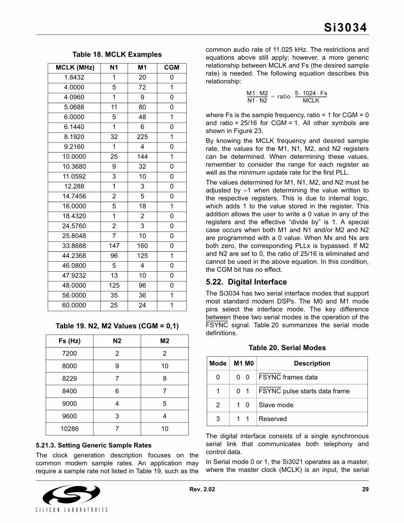
Table 18. MCLK Examples
MCLK (MHz) N1 M1 CGM1.8432 1 20 04.0000 5 72 14.0960 1 9 05.0688 11 80 06.0000 5 48 16.1440 1 6 08.1920 32 225 19.2160 1 4 010.0000 25 144 110.3680 9 32 011.0592 3 10 012.288 1 3 014.7456 2 5 016.0000 5 18 118.4320 1 2 024.5760 2 3 025.8048 7 10 033.8688 147 160 044.2368 96 125 146.0800 5 4 047.9232 13 10 048.0000 125 96 056.0000 35 36 160.0000 25 24 1
Table 19. N2, M2 Values (CGM = 0,1)
Fs (Hz) N2 M2
7200 2 2
8000 9 10
8229 7 8
8400 6 7
9000 4 5
9600 3 4
10286 7 10
Table 20. Serial Modes
Mode M1 M0 Description
0 0 0 FSYNC frames data
1 0 1 FSYNC pulse starts data frame
2 1 0 Slave mode
3 1 1 Reserved
M1 M2⋅N1 N2⋅--------------------- ratio 5 1024 Fs⋅ ⋅
MCLK--------------------------------⋅=

Si3034
30 Rev. 2.02
data clock (SCLK) is an output, and the frame syncsignal (FSYNC) is an output. The MCLK frequency andthe value of the sample rate control registers 7, 8, 9 and10 determine the sample rate (Fs). The serial port clock,SCLK, runs at 256 bits per frame, where the frame rateis equivalent to the sample rate. Refer to "5.21. ClockGeneration Subsystem‚" on page 27 for more details onprogramming sample rates.The Si3034 transfers 16-bit or 15-bit telephony data inthe primary timeslot and 16-bit control data in thesecondary timeslot. Figure 24 and 25 on page 34 showthe relative timing of the serial frames. Primary framesoccur at the frame rate and are always present. Tominimize overhead in the external DSP, secondaryframes are present only when requested.Two methods exist for transferring control information inthe secondary frame. The default power-up mode usesthe LSB of the 16-bit transmit (TX) data word as a flag torequest a secondary transfer. In this mode, only 15-bitTX data is transferred, resulting in a loss of SNR butallowing software control of the secondary frames. Asan alternative method, the FC pin can serve as ahardware flag for requesting a secondary frame. Theexternal DSP can turn on the 16-bit TX mode by settingthe SB bit in Register 1. In the 16-bit TX mode, thehardware FC pin must be used to request secondarytransfers.Figure 26 and Figure 27 illustrate the secondary frameread cycle and write cycle, respectively. During a readcycle, the R/W bit is high, and the 5-bit address fieldcontains the address of the register to be read. Thecontents of the 8-bit control register are placed on theSDO signal. During a write cycle, the R/W bit is low, andthe 5-bit address field contains the address of theregister to be written. The 8-bit data to be writtenimmediately follows the address on SDI. Only oneregister can be read or written during each secondaryframe. See "6. Control Registers‚" on page 41 for theregister addresses and functions.In serial mode 2, the Si3021 operates as a slave devicewhere the MCLK is an input, the SCLK is a no connect(except for the master device for which it is an output),and the FSYNC is an input. In addition, the RGDT/FSDpin operates as a delayed frame sync (FSD), and theFC/RGDT pin operates as ring detect (RGDT). Notethat in this mode, FC operation is not supported. Forfurther details on operating the Si3021 as a slavedevice, refer to “30 Multiple Device Support”.
5.23. Multiple Device SupportThe Si3034 supports the operation of up to sevenadditional devices on a single serial interface. Figure 32shows the typical connection of the Si3034 and oneadditional serial voice codec (Si3000).The Si3034 must be the master in this configuration.The secondary codec should be configured as a slavedevice with SCLK and FSYNC as inputs. Upon powerup, the Si3034 master will be unaware of the additionalcodec on the serial bus. The FC/RGDT pin is an inputoperating as the hardware control for secondary frames,and the RGDT/FSD pin is an output operating as theactive low ring detection signal. The master deviceshould be programmed for master/slave mode prior toenabling the isolation capacitor link because a ringsignal would cause a false transition to the slavedevice’s FSYNC.Register 14 provides the necessary control bits toconfigure the Si3034 for master/slave operation. Bit 0(DCE) sets the Si3034 in master/slave mode, alsoreferred to as daisy-chain mode. When the DCE bit isset, the FC/RGDT pin becomes the ring detect output,and the RGDT/FSD pin becomes the frame sync delayoutput.Bits 7:5 (NSLV2:NSLV0) set the number of slaves to besupported on the serial bus. For each slave, the Si3034will generate a FSYNC to the DSP. In daisy-chain mode,the polarity of the ring signal can be controlled by bit 1(RPOL). When RPOL = 1, the ring detect signal (nowoutput on the FC/RGDT pin) is active high.The Si3034 supports a variety of codecs as well asadditional Si3034s. The type of slave codec(s) used isset by bits 4:3 (SSEL1:SSEL0). These bits determinethe type of signalling used in the LSB of SDO. Thisassists the DSP in isolating which data stream is themaster and which is the slave. If the LSB is used forsignalling, the master device will have a unique settingrelative to the slave devices. The DSP can use thisinformation to determine which FSYNC marks thebeginning of a sequence of data transfers.The delayed frame sync (FSD) of each device issupplied as the FSYNC of each subsequent slavedevice in the daisy chain. The master Si3034 willgenerate an FSYNC signal for each device every 16 or32 SLCK periods. The delay period is set byRegister 14, bit 2 (FSD). Figures 28–31 show therelative timing for daisy chaining operation.

Si3034
Rev. 2.02 31
Note that primary communication frames occur insequence, followed by secondary communicationframes, if requested. When writing/reading the masterdevice via a secondary frame, all secondary frames ofthe slave devices must be written as well. When writing/reading a slave device via a secondary frame, thesecondary frames of the master and all other slavesmust be written as well. "No operation" writes/reads tosecondary frames are accomplished by writing/readinga zero value to address zero.If FSD is set for 16 SCLK periods between FSYNCs,only serial mode 1 can be used. In addition, the slavedevices must delay the tri-state to active transition oftheir SDO sufficiently from the rising edge of SCLK toavoid bus contention.The Si3034 supports the operation of up to eight Si3034devices on a single serial bus. The master Si3034 mustbe configured in serial mode 1. The slave(s) Si3034 isconfigured in serial mode 2. 33 on page 40 shows atypical master/slave connection using three Si3034devices.When in serial mode 2, FSYNC becomes an input,RGDT/FSD becomes the delay frame sync output, andFC/RGDT becomes the ring detection output. Inaddition, the internal PLLs are fixed to a “multiply by20”. This provides the desired sample rate when themaster’s SCLK is provided to the slave’s MCLK. Notethat the SCLK of the slave is a no connect in thisconfiguration.The delay between FSYNC input and delayed framesync output (RGDT/FSD) will be 16 SCLK periods. TheRGDT/FSD output has a waveform identical to theFSYNC signal in serial mode 0. In addition, the LSB ofSDO is set to zero by default for all devices in serialmode 2.
5.24. Power ManagementThe Si3034 supports four basic power managementoperation modes. The modes are normal operation,reset operation, sleep mode, and full power downmode. The power management modes are controlled bythe PDN and PDL bits in Register 6.Upon power up or following a reset, the Si3034 is inreset operation. In this mode, the PDL bit is set, whilethe PDN bit is cleared. The Si3021 is fully-operationalexcept for the isolation capacitor link. Nocommunication between the Si3021 and Si3014 canoccur during reset operation. Any bits associated withthe Si3014 are not valid in this mode.The most common mode of operation is normaloperation. In this mode, the PDL and PDN bits arecleared. The Si3021 is fully-operational, and the
isolation capacitor link is passing information betweenthe Si3021 and the Si3014. The clock generator mustbe programmed to a valid sample rate prior to enteringthis mode.The Si3034 supports a low-power sleep mode. Thismode supports the popular wake-up-on-ring feature ofmany modems. The clock generator registers, 7, 8, and9, must be programmed with valid non-zero values priorto enabling sleep mode. Then, the PDN bit must be setand the PDL bit cleared. When the Si3034 is in sleepmode, the MCLK signal may be stopped or remainactive, but it must be active before waking up theSi3034. The Si3021 is non-functional except for theisolation capacitor and RGDT signal. To take the Si3034out of sleep mode, pulse the reset pin (RESET) low.In summary, the power down/up sequence for sleepmode is as follows:1. Registers 7, 8, and 9 must have valid non-zero values.2. Set the PDN bit (Register 6, bit 3) and clear the PDL bit
(Register 6, bit 4).3. MCLK may stay active or stop.4. Restore MCLK before initiating the power-up sequence.5. Reset the Si3034 using RESET pin (after MCLK is
present).6. Program registers to desired settings. The Si3034 also supports an additional power-downmode. When both the PDN (Register 6, bit 3) and PDL(Register 6, bit 4) are set, the chipset enters a completepower-down mode and draws negligible current (deepsleep mode). PLL2 should be turned off prior to enteringdeep sleep mode (i.e., set Register 9 to 0 and thenRegister 6 to 0x18). In this mode, the RGDT pin doesnot function. Normal operation may be restored usingthe same process for taking the chipset out of sleepmode.
5.25. CalibrationThe Si3034 initiates an auto-calibration by defaultwhenever the device goes off-hook or experiences aloss in line power. Calibration is used to remove anyoffsets that may be present in the on-chip A/D converterwhich could affect the A/D dynamic range. Auto-calibration is typically initiated after the DAA dctermination stabilizes and takes 512/Fs seconds tocomplete. Due to the large variation in line conditionsand line card behavior that can be presented to theDAA, it may be beneficial to use manual calibration inlieu of auto-calibration. Manual calibration should be executed as close to 512/Fs seconds before valid transmit/receive data isexpected.The following steps should be taken to implement
Si3034
32 Rev. 2.02
manual calibration:1. The CALD (auto-calibration disable—Register 17) bit must
be set to 1. 2. The MCAL (manual calibration) bit must be toggled to one
and then zero to begin and complete the calibration. 3. The calibration will be completed in 512/Fs seconds.
5.26. In-Circuit TestingThe Si3034’s advanced design provides the modemmanufacturer with increased ability to determine systemfunctionality during production line tests, as well assupport for end-user diagnostics. Four loopback modesexist allowing increased coverage of systemcomponents. For three of the test modes, a line-sidepower source is needed. While a standard phone linecan be used, the test circuit in 1 on page 5 is adequate.In addition, an off-hook sequence must be performed toconnect the power source to the line-side chip. For the start-up test mode, no line-side power isnecessary and no off-hook sequence is required. Thestart-up test mode is enabled by default. When the PDLbit (Register 6, bit 4) is set (the default case), the lineside is in a power-down mode and the DSP side is in adigital loop-back mode. In this mode, data received onSDI is passed through the internal filters and transmittedon SDO. This path will introduce approximately 0.9 dBof attenuation on the SDI signal received. The groupdelay of both transmit and receive filters will existbetween SDI and SDO. Clearing the PDL bit disablesthis mode and the SDO data is switched to the receivedata from the line side. When PDL is cleared the FDTbit (Register 12, bit 6) will become active, indicating thesuccessful communication between the line side andDSP side. This can be used to verify that the isolationcapacitor is operational.The remaining test modes require an off-hook sequenceto operate. The following sequence defines the off-hookrequirement:1. Power up or reset.2. Program clock generator to desired sample rate.3. Enable line-side by clearing PDL bit.4. Issue off-hook. 5. Delay 1548/Fs sec to allow calibration to occur. 6. Set desired test mode. The isolation capacitor digital loopback mode allows thedata pump to provide a digital input test pattern on SDIand receive that digital test pattern back on SDO. Toenable this mode, set the DL bit in Register 1. In thismode, the isolation barrier is actually being tested. Thedigital stream is delivered across the isolation capacitor,C1 of 16 on page 15, to the line-side device andreturned across the same barrier. In this mode, the
0.9 dB attenuation and filter group delays also exist.The analog loopback mode allows an external device todrive a signal on the telephone line into the Si3034 line-side device and have it driven back out onto the line.This mode allows testing of external componentsconnecting the RJ-11 jack (TIP and RING) to theSi3014. To enable this mode, set the AL bit inRegister 2.The final testing mode, internal analog loopback, allowsthe system to test the basic operation of the transmitand receive paths on the line-side chip and the externalcomponents in 16 on page 15. In this test mode, thedata pump provides a digital test waveform on SDI. Thisdata is passed across the isolation barrier, transmittedto and received from the line, passed back across theisolation barrier, and presented to the data pump onSDO. To enable this mode, clear the HBE bit inRegister 2.When the HBE bit is cleared, this will cause a dc offset,which affects the signal swing of the transmit signal. Inthis test mode, it is recommended that the transmitsignal be 12 dB lower than normal transmit levels. Thislower level will eliminate clipping caused by the dcoffset, which results from disabling the hybrid. In thistest, it is assumed that the line ac impedance isnominally 600 Ω.Note: All test modes are mutually exclusive. If more than one
test mode is enabled concurrently, the results areunpredictable.
5.27. Exception HandlingThe Si3034 provides several mechanisms to determineif an error occurs during operation. Through thesecondary frames of the serial link, the controlling DSPcan read several status bits. The bit of highestimportance is the frame detect bit (FDT, Register 12,bit 6). This bit indicates that the DSP-side (Si3021) andline-side (Si3014) devices are communicating. Duringnormal operation, the FDT bit can be checked beforereading any bits that indicate information about the lineside. If FDT is not set, the following bits related to theline-side are invalid: RDT, RDTN, RDTP, LCS[3:0],CBID, REVB[3:0], CTRO, and OVL. The RGDToperation will also be non-functional.Following power-up and reset, the FDT bit is not setbecause the PDL bit (Register 6, bit 4) defaults to 1. Inthis state, the isolation capacitor link is not operating,and no information about the line-side can bedetermined. The user must program the clock generatorto a valid configuration for the system and clear the PDLbit to activate the isolation capacitor link. While the DSPand line side are establishing communication, the DSP-side does not generate FSYNC signals. Establishing

Si3034
Rev. 2.02 33
communication will take less than 10 ms. Therefore, ifthe controlling DSP serial interface is interrupt driven,based on the FSYNC signal, the controlling DSP doesnot require a special delay loop to wait for this event tocomplete.The FDT bit can also indicate if the line-side executesan off-hook request successfully. If the line-side is notconnected to a phone line (i.e., the user fails to connecta phone line to the modem), the FDT bit remainscleared. The controlling DSP must allow sufficient timefor the line-side to execute the off-hook request. Themaximum time for FDT to be valid following an off-hookrequest is 10 ms. If the FDT is high, the LCS[3:0] bitsindicate the amount of loop current flowing. If the FDTfails to be set following an off-hook request, the PDL bitin Register 6 must be set high for at least 1 ms to resetthe line side. Another useful bit is the communication link error (CLE)bit (Register 12, bit 7). The CLE bit indicates a time-outerror for the isolation capacitor link following a changeto either PLL1 or PLL2. When the CLE bit is set, theDSP-side chip has failed to receive verification from theline-side that the clock change has been accepted in anexpected period of time (less than 10 ms). Thiscondition indicates a severe error in programming theclock generator or possibly a defective line-side chip.
5.28. Revision IdentificationThe Si3034 provides the system designer the ability todetermine the revision of the Si3021 and/or the Si3014.The REVA[3:0] bits in Register 11 identify the revision ofthe Si3021. The REVB[3:0] and CBID bits in Register 13identify the revision of the Si3014.‘
Table 21. Revision Values
Revision Si3021 Si3014
A 1000 0001
B 1001 0010
C 1010 0011

Si3034
34 Rev. 2.02
Figure 24. Software FC/RGDT Secondary Request
Figure 25. Hardware FC/RGDT Secondary Request
Communications Frame 1 (CF1) (CF2)
16 SCLKS
128 SCLKS
256 SCLKS
PrimaryFSYNC
FC 0
XMT Data SecondaryData
XMT DataSDI
RCV DataSecondary
Data RCV DataSDO
D15 –D1 D0 = 1 (Software FC Bit)
Secondary Primary
D15 –D1 D0 = 0 (Software FC Bit)
Communications Frame 1 (CF1) (CF2)
16 SCLKS
128 SCLKS
256 SCLKS
PrimaryFSYNC
FC 0
XMT DataSecondary
DataXMT DataSDI
RCV DataSecondary
DataRCV DataSDO
D15–D0
Secondary Primary

Si3034
Rev. 2.02 35
Figure 26. Secondary Communication Data Format—Read Cycle
Figure 27. Secondary Communication Data Format—Write Cycle
R/W
FSYNC(mode 1)
SDID15 D14 D13 D12 D11 D10 D9 D8 D7 D0
0 0 1 A A A A A
SDO D
D7 D6 D5 D4 D3 D2 D1 D0
D D D D D D D
FSYNC(mode 0)
R/W
FSYNC(mode 1)
SDID15 D14 D13 D12 D11 D10 D9 D8 D7 D6 D5 D4 D3 D2 D1 D0
0 0 0 A A A A A
SDO
D D D D D D D D
FSYNC(mode 0)

Si3034
36 Rev. 2.02
Figure 28. Daisy Chaining of a Single Slave (Pulse FSD)
Figure 29. Daisy Chaining of a Single Slave (Frame FSD)
128 SCLKs 128 SCLKs
32 SCLKs 32 SCLKs
Primary Frame (Data) Secondary Frame (Control)
Master
Slave 1
Master FSYNC
Master FSD/Slave1 FSYNC
SDI [0]SDI [15..1]
SDO [0]SDO[15..1]
Comments
Serial Mode 1Reg 14: NSLV = 1, SSEL = 2, FSD = 0, DCE = 1
Serial Mode 2Reg 14 Reset values: NSLV = 1, SSEL = 3, FSD = 1, DCE = 1
1Master
1Slave1
MasterMaster
Slave1Slave1
Slave1Slave1
MasterMaster
0Slave1
1Master
Primary frames with secondary frame requested via SDI[0] = 1
128 SCLKs 128 SCLKs
16 SCLKs
Primary Frame (Data) Secondary Frame (Control)
Master
Slave 1
Master FSYNC
Master FSD/Slave1 FSYNC
SDI [0]SDI [15..1]
SDO [0]SDO[15..1]
Comments
Serial Mode 1Reg 14: NSLV = 1, SSEL = 2, FSD = 1, DCE = 1
Serial Mode 2Reg 14 Reset values: NSLV = 1, SSEL = 3, FSD = 1, DCE = 1
1Master
1Slave1
MasterMaster
Slave1Slave1
Slave1Slave1
MasterMaster
0Slave1
1Master
Primary frames with secondary frame requested via SDI[0] = 1
16 SCLKs 16 SCLKs 16 SCLKs
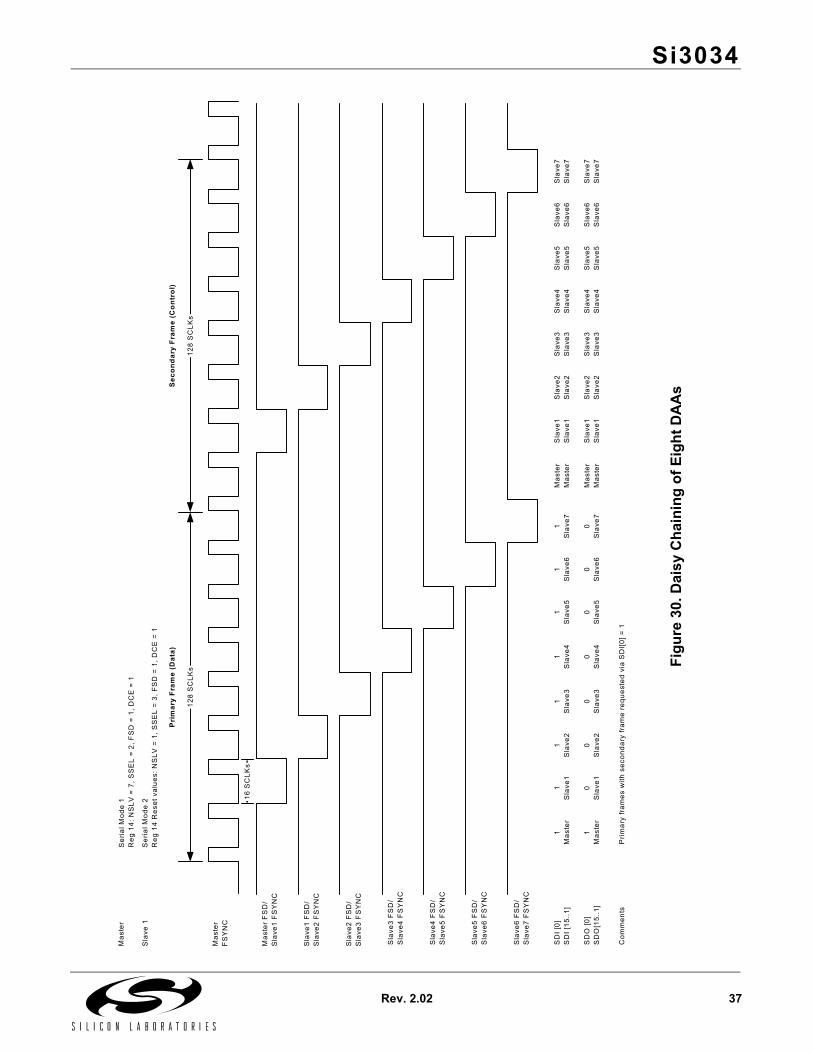
Si3034
Rev. 2.02 37
Mas
ter
Sla
ve 1
Mas
ter
FS
YN
C
Mas
ter
FS
D/
Sla
ve1
FS
YN
C
Ser
ial M
ode
1R
eg 1
4: N
SLV
= 7
, SS
EL
= 2,
FS
D =
1, D
CE
= 1
Ser
ial M
ode
2R
eg 1
4 R
eset
val
ues:
NS
LV =
1, S
SE
L =
3, F
SD
= 1
, DC
E =
1
Sla
ve1
FS
D/
Sla
ve2
FS
YN
C
Sla
ve2
FS
D/
Sla
ve3
FS
YN
C
Sla
ve3
FS
D/
Sla
ve4
FS
YN
C
Sla
ve4
FS
D/
Sla
ve5
FS
YN
C
Sla
ve5
FS
D/
Sla
ve6
FS
YN
C
Sla
ve6
FS
D/
Sla
ve7
FS
YN
C
SD
I [0]
SD
I [15
..1]
SD
O [0
]S
DO
[15.
.1]
Com
men
ts
128
SC
LKs
Sec
ond
ary
Fra
me
(Co
ntro
l)
128
SC
LKs
Pri
mar
y F
ram
e (D
ata)
16 S
CLK
s
Mas
ter
Mas
ter
Sla
ve1
Sla
ve1
Sla
ve1
Sla
ve1
Mas
ter
Mas
ter
Prim
ary
fram
es w
ith s
econ
dary
fram
e re
ques
ted
via
SD
I[0] =
1
Sla
ve2
Sla
ve2
Sla
ve3
Sla
ve3
Sla
ve5
Sla
ve5
Sla
ve4
Sla
ve4
Sla
ve6
Sla
ve6
Sla
ve7
Sla
ve7
Sla
ve2
Sla
ve2
Sla
ve3
Sla
ve3
Sla
ve5
Sla
ve5
Sla
ve4
Sla
ve4
Sla
ve6
Sla
ve6
Sla
ve7
Sla
ve7
1M
aste
r
1M
aste
r
1S
lave
1
0S
lave
1
1S
lave
2
0S
lave
2
1S
lave
3
0S
lave
3
1S
lave
4
0S
lave
4
1S
lave
5
0S
lave
5
1S
lave
6
0S
lave
6
1S
lave
7
0S
lave
7
Figu
re30
.Dai
sy C
hain
ing
of E
ight
DA
As

Si3034
38 Rev. 2.02
Figure 31. Daisy Chaining with Framed FSYNC and Framed FSD
Primary Frame (Data) Secondary Frame (Control)
Master
Slave 1
Master FSD/Slave1 FSYNC
SDI [0]SDI [15..1]
SDO [0]SDO [15..1]
Comments Primary frames with secondary frame requested via SDI[0] = 1
128 SCLKs 128 SCLKs
16 SCLKs
Master FSYNC
Slave1Slave1
Slave1Slave1
MasterMaster
MasterMaster
1Slave1
0Slave1
1Master
1Master
Serial Mode 0Reg 14: NSLV = 1, SSEL = 2, FSD = 0, DCE = 1
Serial Mode 2Reg 14 Reset values: NSLV = 1, SSEL = 3, FSD = 1, DCE = 1
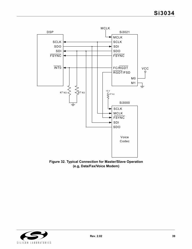
Si3034
Rev. 2.02 39
Figure 32. Typical Connection for Master/Slave Operation(e.g, Data/Fax/Voice Modem)
SCLKSDO
SDI
INT0
FSYNC
SCLK
SDOSDI
FSYNC
MCLK
FC/RGDTRGDT/FSD
SCLK
SDOSDIFSYNCMCLK
MCLKDSP Si3021
Si3000
47 kΩ 47 kΩ47 kΩ
+5 V
M0M1
VCC
VoiceCodec

Si3034
40 Rev. 2.02
Figure 33. Typical Connection for Multiple Si3034s
SCLKSDO
SDIFSYNC
SCLK
SDOSDI
FSYNC
MCLK
FC/RGDTRGDT/FSD
M1M0
SCLK
SDOSDIFSYNC
MCLK
M1M0
SCLK
SDOSDIFSYNC
MCLK
M1M0
RGDT/FSD
MCLKDSP Si3021–Master
Si3021–Slave 1
Si3021–Slave 2
VCC
47 kΩ 47 kΩ
VCC
VCC
INT0
RGDT/FSD
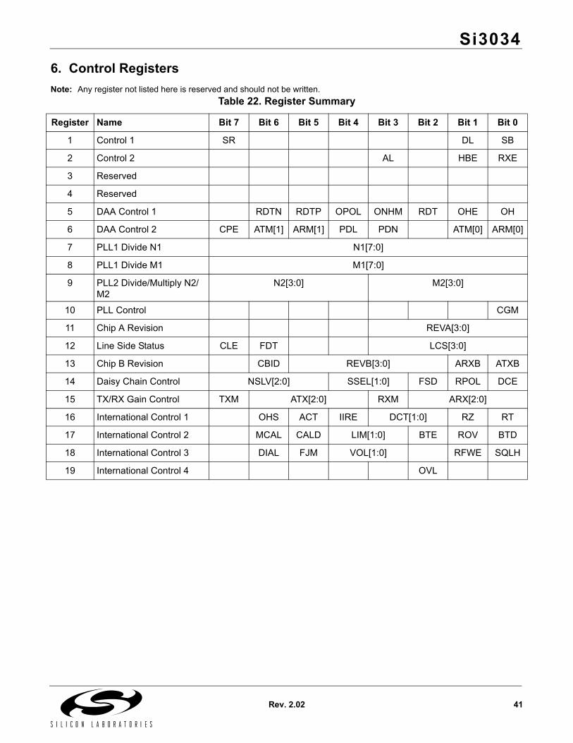
Si3034
Rev. 2.02 41
6. Control RegistersNote: Any register not listed here is reserved and should not be written.
Table 22. Register Summary
Register Name Bit 7 Bit 6 Bit 5 Bit 4 Bit 3 Bit 2 Bit 1 Bit 0
1 Control 1 SR DL SB
2 Control 2 AL HBE RXE
3 Reserved
4 Reserved
5 DAA Control 1 RDTN RDTP OPOL ONHM RDT OHE OH
6 DAA Control 2 CPE ATM[1] ARM[1] PDL PDN ATM[0] ARM[0]
7 PLL1 Divide N1 N1[7:0]
8 PLL1 Divide M1 M1[7:0]
9 PLL2 Divide/Multiply N2/M2
N2[3:0] M2[3:0]
10 PLL Control CGM
11 Chip A Revision REVA[3:0]
12 Line Side Status CLE FDT LCS[3:0]
13 Chip B Revision CBID REVB[3:0] ARXB ATXB
14 Daisy Chain Control NSLV[2:0] SSEL[1:0] FSD RPOL DCE
15 TX/RX Gain Control TXM ATX[2:0] RXM ARX[2:0]
16 International Control 1 OHS ACT IIRE DCT[1:0] RZ RT
17 International Control 2 MCAL CALD LIM[1:0] BTE ROV BTD
18 International Control 3 DIAL FJM VOL[1:0] RFWE SQLH
19 International Control 4 OVL

Si3034
42 Rev. 2.02
Reset settings = 0000_0000
Reset settings = 0000_0011
Register 1. Control 1
Bit D7 D6 D5 D4 D3 D2 D1 D0
Name SR DL SB
Type R/W R/W R/W
Bit Name Function7 SR Software Reset.
0 = Enables chip for normal operation. 1 = Sets all registers to their reset value.Note: Bit will automatically clear after being set.
6:2 Reserved Read returns zero.1 DL Isolation Digital Loopback.
0 = Digital loopback across the isolation barrier disabled.1 = Enables digital loopback mode across the isolation barrier. The line-side must be enabled prior to setting this mode.
0 SB Serial Digital Interface Mode.0 = Operation is in 15-bit mode, and the LSB of the data field indicates whether a secondary frame is required.1 = The serial port is operating in 16-bit mode and requires use of the secondary frame sync signal (FC) to initiate control data reads/writes.
Register 2. Control 2
Bit D7 D6 D5 D4 D3 D2 D1 D0
Name AL HBE RXE
Type R/W R/W R/W
Bit Name Function7:4 Reserved Read returns zero.3 AL Analog Loopback.
0 = Analog loopback mode disabled.1 = Enables external analog loopback mode.
2 Reserved Read returns zero.1 HBE Hybrid Enable.
0 = Disconnects hybrid in transmit path.1 = Connects hybrid in transmit path.
0 RXE Receive Enable.0 = Receive path disabled.1 = Enables receive path.

Si3034
Rev. 2.02 43
Reset settings = 0000_0000
Reset settings = 0000_0000
Register 3. Reserved
Bit D7 D6 D5 D4 D3 D2 D1 D0
Name
Type
Bit Name Function
7:0 Reserved Read returns zero.
Register 4. Reserved
Bit D7 D6 D5 D4 D3 D2 D1 D0
Name
Type
Bit Name Function
7:0 Reserved Read returns zero.

Si3034
44 Rev. 2.02
Reset settings = 0000_0000
Register 5. DAA Control 1
Bit D7 D6 D5 D4 D3 D2 D1 D0
Name RDTN RDTP OPOL ONHM RDT OHE OH
Type R R R/W R/W R R/W R/W
Bit Name Function
7 Reserved Read returns zero.
6 RDTN Ring Detect Signal Negative.0 = No negative ring signal is occurring.1 = A negative ring signal is occurring.
5 RDTP Ring Detect Signal Positive.0 = No positive ring signal is occurring.1 = A positive ring signal is occurring.
4 OPOL Off-Hook Polarity.0 = Off-hook pin is active low.1 = Off-hook pin is active high.
3 ONHM On-Hook Line Monitor. 0 = Normal on-hook mode.1 = Enables low-power monitoring mode allowing the DSP to receive line activity without going off-hook. This mode is used for caller-ID detection.
2 RDT Ring Detect. 0 = Reset either 4.5–9 seconds after last positive ring is detected or when the system exe-cutes an off-hook.1 = Indicates a ring is occurring.
1 OHE Off-Hook Pin Enable.0 = Off-hook pin is ignored.1 = Enables the operation of the off-hook pin.
0 OH Off-Hook. 0 = Line-side device is on-hook.1 = Causes the line-side chip to go off-hook. This bit operates independently of the OHE bit and is a logic OR with the off-hook pin when enabled.

Si3034
Rev. 2.02 45
Reset settings = 0111_0000
Reset settings = 0000_0000 (serial mode 0, 1, 2)
Register 6. DAA Control 2
Bit D7 D6 D5 D4 D3 D2 D1 D0
Name CPE ATM[1] ARM[1] PDL PDN ATM[0] ARM[0]
Type R/W R/W R/W R/W R/W R/W R/W
Bit Name Function
7 CPE Charge Pump Enable.0 = Charge pump is disabled.1 = Charge pump is enabled.If the charge pump is not to be enabled, R3 must be installed with 10 Ω, 1/10 W and VD must be between 4.75 and 5.25 V.
6,1 ATM[1:0] AOUT Transmit Path Level Control.00 = –20 dB transmit path attenuation for call progress AOUT pin only.01 = –32 dB transmit path attenuation for call progress AOUT pin only.10 = Mutes transmit path for call progress AOUT pin only.11 = –26 dB transmit path attenuation for call progress AOUT pin only.
5,0 ARM[1:0] AOUT Receive Path Level Control.00 = 0 dB receive path attenuation for call progress AOUT pin only.01 = –12 dB receive path attenuation for call progress AOUT pin only.10 = Mutes receive path for call progress AOUT pin only.11 = –6 dB receive path attenuation for call progress AOUT pin only.
4 PDL Power Down Line-Side Chip.0 = Normal operation. Program the clock generator before clearing this bit.1 = Places the Si3014 in lower power mode.
3 PDN Power Down.0 = Normal operation.1 = Powers down the Si3021. A pulse on RESET is required to restore normal operation.
2 Reserved Read returns zero.
Register 7. PLL1 Divide N1
Bit D7 D6 D5 D4 D3 D2 D1 D0
Name N1
Type R/W
Bit Name Function
7:0 N1[7:0] PLL N1 Divider. Contains the (value – 1) for determining the output frequency on PLL1.

Si3034
46 Rev. 2.02
Reset settings = 0000_0000 (serial mode 0, 1)
Reset settings = 0001_0011 (serial mode 2)
Reset settings = 0000_0000
Reset settings = 0000_0000
Register 8. PLL1 Multiply M1
Bit D7 D6 D5 D4 D3 D2 D1 D0
Name M1
Type R/W
Bit Name Function
7:0 M1[7:0] PLL1 M1 Multiplier. Contains the (value – 1) for determining the output frequency on PLL1.
Register 9. PLL2 Divide/Multiply N2/M2
Bit D7 D6 D5 D4 D3 D2 D1 D0
Name N2 M2
Type R/W R/W
Bit Name Function
7:4 N2[3:0] PLL2 N2 Divider.Contains the (value – 1) for determining the output frequency on PLL2.
3:0 M2[3:0] PLL2 M2 Multiplier.Contains the (value – 1) for determining the output frequency on PLL2.
Register 10. PLL Control
Bit D7 D6 D5 D4 D3 D2 D1 D0
Name CGM
Type R/W
Bit Name Function
7:1 reserved Read returns zero.
0 CGM Clock Generation Mode.0 = No additional ratio is applied to the PLL and faster lock times are possible.1 = A 25/16 ratio is applied to the PLL allowing for a more flexible choice of MCLK frequencies while slowing down the PLL lock time.

Si3034
Rev. 2.02 47
Reset settings = N/A
Reset settings = N/A
Register 11. Chip A Revision
Bit D7 D6 D5 D4 D3 D2 D1 D0
Name REVA[3:0]
Type R
Bit Name Function
7:4 Reserved Read returns zero.
3:0 REVA[3:0] Chip A Revision.Four-bit value indicating the revision of the Si3021 (DSP-side) chip.
Register 12. Line-Side Status
Bit D7 D6 D5 D4 D3 D2 D1 D0
Name CLE FDT LCS[3:0]
Type R/W R R
Bit Name Function
7 CLE Communications (Isolation Capacitor link) Error. 0 = Isolation capacitor communication link between the Si3021 and the Si3014 is operating correctly.1 = Indicates a communication problem between the Si3021 and the Si3014. When it goes high, it remains high until a logic 0 is written to it.
6 FDT Frame Detect. 0 = Indicates isolation capacitor link has not established frame lock.1 = Indicates isolation capacitor link frame lock has been established.
5:4 Reserved Read returns zero.
3:0 LCS[3:0] Loop Current Sense. Four-bit value returning the loop current in 6 mA increments.0 = Loop current < 0.4 mA typical.1111 = Loop current > 155 mA typical. See "5.16. Loop Current Monitor‚" on page 26.
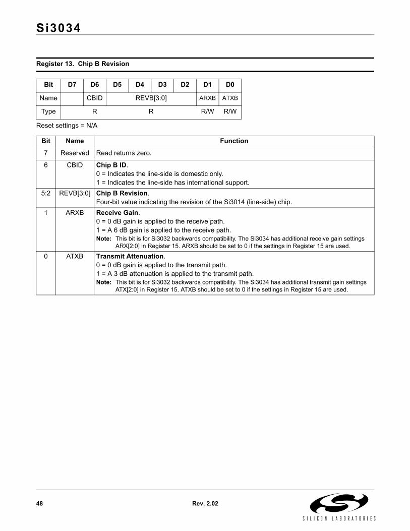
Si3034
48 Rev. 2.02
Reset settings = N/A
Register 13. Chip B Revision
Bit D7 D6 D5 D4 D3 D2 D1 D0
Name CBID REVB[3:0] ARXB ATXB
Type R R R/W R/W
Bit Name Function
7 Reserved Read returns zero.
6 CBID Chip B ID.0 = Indicates the line-side is domestic only.1 = Indicates the line-side has international support.
5:2 REVB[3:0] Chip B Revision.Four-bit value indicating the revision of the Si3014 (line-side) chip.
1 ARXB Receive Gain.0 = 0 dB gain is applied to the receive path.1 = A 6 dB gain is applied to the receive path. Note: This bit is for Si3032 backwards compatibility. The Si3034 has additional receive gain settings
ARX[2:0] in Register 15. ARXB should be set to 0 if the settings in Register 15 are used.
0 ATXB Transmit Attenuation.0 = 0 dB gain is applied to the transmit path.1 = A 3 dB attenuation is applied to the transmit path. Note: This bit is for Si3032 backwards compatibility. The Si3034 has additional transmit gain settings
ATX[2:0] in Register 15. ATXB should be set to 0 if the settings in Register 15 are used.
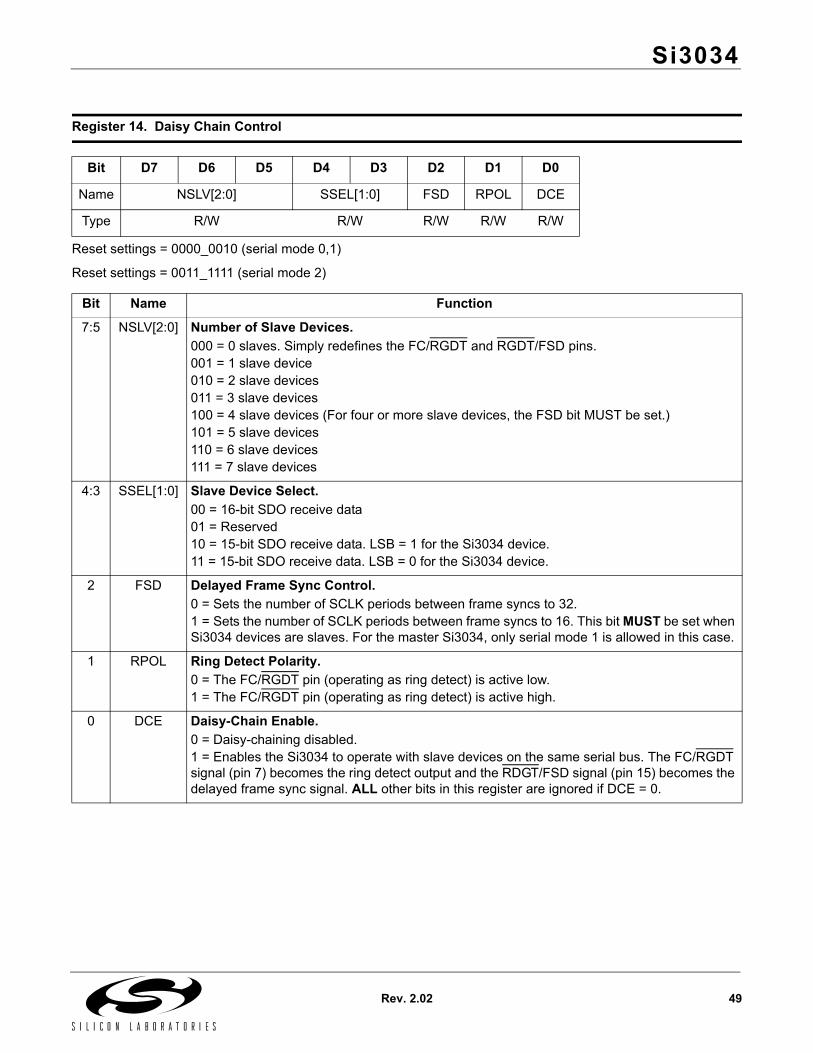
Si3034
Rev. 2.02 49
Reset settings = 0000_0010 (serial mode 0,1)
Reset settings = 0011_1111 (serial mode 2)
Register 14. Daisy Chain Control
Bit D7 D6 D5 D4 D3 D2 D1 D0
Name NSLV[2:0] SSEL[1:0] FSD RPOL DCE
Type R/W R/W R/W R/W R/W
Bit Name Function
7:5 NSLV[2:0] Number of Slave Devices.000 = 0 slaves. Simply redefines the FC/RGDT and RGDT/FSD pins.001 = 1 slave device010 = 2 slave devices011 = 3 slave devices100 = 4 slave devices (For four or more slave devices, the FSD bit MUST be set.)101 = 5 slave devices110 = 6 slave devices111 = 7 slave devices
4:3 SSEL[1:0] Slave Device Select.00 = 16-bit SDO receive data01 = Reserved10 = 15-bit SDO receive data. LSB = 1 for the Si3034 device.11 = 15-bit SDO receive data. LSB = 0 for the Si3034 device.
2 FSD Delayed Frame Sync Control.0 = Sets the number of SCLK periods between frame syncs to 32.1 = Sets the number of SCLK periods between frame syncs to 16. This bit MUST be set when Si3034 devices are slaves. For the master Si3034, only serial mode 1 is allowed in this case.
1 RPOL Ring Detect Polarity.0 = The FC/RGDT pin (operating as ring detect) is active low.1 = The FC/RGDT pin (operating as ring detect) is active high.
0 DCE Daisy-Chain Enable. 0 = Daisy-chaining disabled.1 = Enables the Si3034 to operate with slave devices on the same serial bus. The FC/RGDT signal (pin 7) becomes the ring detect output and the RDGT/FSD signal (pin 15) becomes the delayed frame sync signal. ALL other bits in this register are ignored if DCE = 0.

Si3034
50 Rev. 2.02
Reset settings = 0000_0000
Register 15. TX/RX Gain Control
Bit D7 D6 D5 D4 D3 D2 D1 D0
Name TXM ATX[2:0] RXM ARX[2:0]
Type R/W R/W R/W R/W
Bit Name Function
7 TXM Transmit Mute. 0 = Transmit signal is not muted.1 = Mutes the transmit signal.
6:4 ATX[2:0] Analog Transmit Attenuation.000 = 0 dB attenuation001 = 3 dB attenuation010 = 6 dB attenuation011 = 9 dB attenuation1xx = 12 dB attenuationNote: Register 13 ATXB bit must be 0 if these bits are used.
3 RXM Receive Mute. 0 = Receive signal is not muted.1 = Mutes the receive signal.
2:0 ARX[2:0] Analog Receive Gain.000 = 0 dB gain001 = 3 dB gain010 = 6 dB gain011 = 9 dB gain1xx = 12 dB gainNote: Register 13 ARXB bit must be 0 if these bits are used.

Si3034
Rev. 2.02 51
Reset settings = 0000_1000
Register 16. International Control 1
Bit D7 D6 D5 D4 D3 D2 D1 D0
Name OHS ACT IIRE DCT[1:0] RZ RT
Type R/W R/W R/W R/W R/W R/W
Bit Name Function
7 Reserved Read returns zero.
6 OHS On-Hook Speed.0 = The Si3034 will execute a fast on-hook.1 = The Si3034 will execute a slow, controlled on-hook.
5 ACT AC Termination Select.0 = Selects the real impedance.1 = Selects the complex impedance.
4 IIRE IIR Filter Enable.0 = FIR filter enabled for transmit and receive filters. (See Figures 6–9 on page 13.)1 = IIR filter enabled for transmit and receive filters. (See Figures 10–15 on page 14.)
3:2 DCT[1:0] DC Termination Select.00 = Reserved01 = Japan Mode. Low voltage mode. (Transmit level = –3 dBm).10 = FCC Mode. Standard voltage mode. (Transmit level = –1 dBm).11 = TBR21 Mode. Current limiting mode. (Transmit level = –1 dBm).
1 RZ Ringer Impedance.0 = Maximum (high) ringer impedance.1 = Synthesized ringer impedance. C15, R14, Z2, and Z3 must not be installed when setting this bit. See "5.9. Ringer Impedance‚" on page 24.
0 RT Ringer Threshold Select.Used to satisfy country requirements on ring detection. Signals below the lower level will not generate a ring detection; signals above the upper level are guaranteed to generate a ring detection.0 = 11 to 22 VRMS1 = 17 to 33 VRMS

Si3034
52 Rev. 2.02
Reset settings = 0000_0000
Register 17. International Control 2
Bit D7 D6 D5 D4 D3 D2 D1 D0
Name MCAL CALD LIM[1:0] BTE ROV BTD
Type R/W R/W R/W R/W R/W R/W
Bit Name Function
7 Reserved Must be zero.
6 MCAL Manual Calibration.0 = No calibration.1 = Initiate calibration.
5 CALD Auto-Calibration Disable.0 = Auto-calibration enabled.1 = Auto-calibration disabled.
4:3 LIM[1:0] Current Limit.00 = All other modes.11 = TBR21 mode.
2 BTE Billing Tone Detect Enable.0 = Billing tone detection disabled.1 = Billing tone detection enabled.When set, the Si3034 can detect a billing tone signal on the line and maintain off-hook through the billing tone. If a billing tone is detected, the BTD bit in Register 17 will be set to indicate the event.
1 ROV Receive Overload.0 = Normal receive input level.1 = Excessive receive input level.This bit is set if the BTE bit in Register 17 is enabled and the RX pin has an excessive input level. This bit is cleared by writing a 0 to this location.
0 BTD Billing Tone Detected.0 = No billing tone detected.1 = Billing tone detected.This bit will be set if the BTE bit in Register 17 is enabled and a billing tone is detected. This bit is cleared by writing a 0 to this location.

Si3034
Rev. 2.02 53
Reset settings = 0000_0000
Register 18. International Control 3
Bit D7 D6 D5 D4 D3 D2 D1 D0
Name DIAL FJM VOL[1:0] RFWE SQLH
Type R/W R/W R/W R/W R/W
Bit Name Function
7 Reserved Read returns zero.
6 DIAL DTMF Dialing Mode.This bit should be set during DTMF dialing in TBR21 mode if LCS[3:0] < 6.0 = Normal operation.1 = Increase headroom for DTMF dialing.
5 FJM Force Japan DC Termination Mode.0 = Normal Gain.1 = When Register 16, DCT[1:0], is set to 10b (FCC mode), setting this bit will force Japan dc termination mode while allowing for a transmit level of –1 dBm. See “5.10. DTMF Dialing” on page 24.
4:3 VOL[1:0] Line Voltage Adjust.When set, this bit will adjust the TIP-RING line voltage. Lowering this voltage will improve margin in low voltage countries. Raising this voltage may improve distortion performance.00 = Normal01 = –0.125 V10 = 0.25 V11 = 0.125 V
2 Reserved Read returns zero.
1 RFWE Ring Detector Full Wave Rectifier Enable.When set, the ring detection circuitry provides full-wave rectification. This will affect the RGDT pin as well as the data stream presented on SDO during ring detection.0 = Half Wave.1 = Full Wave.
0 SQLH Ring Detect Network Squelch.This bit must be set, then cleared after at least 1 ms, following a polarity reversal or ring signal detection. It is used to quickly recover the offset on the RNG1/2 pins after a polarity reversal or ring signal.0 = Normal operation.1 = Squelch function is enabled.
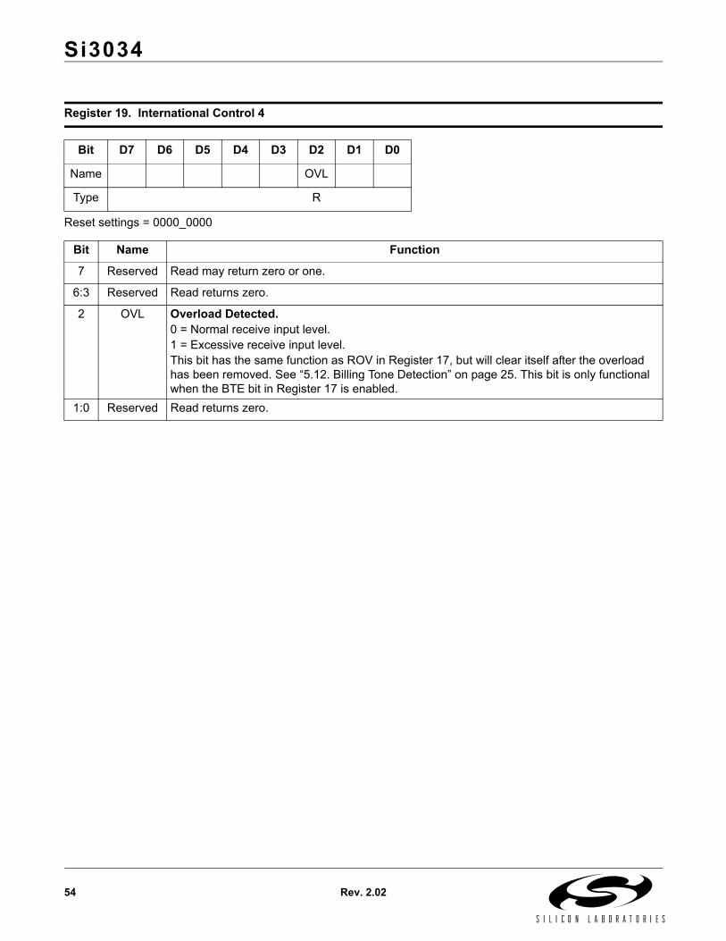
Si3034
54 Rev. 2.02
Reset settings = 0000_0000
Register 19. International Control 4
Bit D7 D6 D5 D4 D3 D2 D1 D0
Name OVL
Type R
Bit Name Function
7 Reserved Read may return zero or one.
6:3 Reserved Read returns zero.
2 OVL Overload Detected.0 = Normal receive input level.1 = Excessive receive input level.This bit has the same function as ROV in Register 17, but will clear itself after the overload has been removed. See “5.12. Billing Tone Detection” on page 25. This bit is only functional when the BTE bit in Register 17 is enabled.
1:0 Reserved Read returns zero.

Si3034
Rev. 2.02 55
APPENDIX A—UL1950 3RD EDITION
Although designs using the Si3034 comply with UL19503rd Edition and pass all overcurrent and overvoltagetests, there are still several issues to consider.Figure 34 shows two designs that can pass the UL1950overvoltage tests, as well as electromagnetic emissions.The top schematic of Figure 34 shows the configurationin which the ferrite beads (FB1, FB2) are on theunprotected side of the sidactor (RV1). For thisconfiguration, the current rating of the ferrite beadsneeds to be 6 A. However, the higher current ferritebeads are less effective in reducing electromagneticemissions.
The bottom schematic of Figure 34 shows theconfiguration in which the ferrite beads (FB1, FB2) areon the protected side of the sidactor (RV1). For thisdesign, the ferrite beads can be rated at 200 mA. In a cost optimized design, it is important to rememberthat compliance to UL1950 does not always requireovervoltage tests. It is best to plan ahead and knowwhich overvoltage tests will apply to your system.System-level elements in the construction, such as fireenclosure and spacing requirements, need to beconsidered during the design stages. Consult with yourprofessional testing agency during the design of theproduct to determine which tests apply to your system.
Figure 34. Circuits that Pass all UL1950 Overvoltage Tests
C24
1.25 A FB1
75 Ω @ 100 MHz, 6 A
TIP
FB2
RING
C25
75 Ω @ 100 MHz, 6 ARV1
C24
1.25 ATIP
RING
C25 600 Ω @ 100 MHz, 200 mA
FB1
FB2
RV1
600 Ω @ 100 MHz, 200 mA

Si3034
56 Rev. 2.02
APPENDIX B—CISPR22 COMPLIANCE
Various countries are expected to adopt the IECCISPR22 standard over the next few years. Forexample, the European Union (EU) has adopted astandard entitled EN55022, which is based on theCISPR22 standard. EN55022 is now part of the EU’sEMC Directive, and compliance is expected to berequired starting in 2003. Adherence to this standardwill be necessary to display the CE mark on designsintended for sale in the EU. The typical schematic andglobal bill of materials (BOM) (see Figure 16 andTable 13) contained in this data sheet are designed tobe compliant to the CISPR22 standard.If smaller inductors are desired, a notch filter may beused and compliance to CISPR22 still achieved. Asshown in Figure 35, a series capacitor-resistor inparallel with L1 and L2 forms the simple notch filter.Table 23 shows corresponding values used for C24,C25, C38, C39, L1, L2, R31, and R32.
Figure 35. Notch Filter for CISPR22 Compliance
The direct current resistance (DCR) of the listedinductors is an important consideration. If the DCR ofthe inductors used is less than 3 Ω each, country PTTspecifications that require 300 Ω or less of dc resistanceat TIP and RING with 20 mA of loop current can besatisfied with the Japan dc termination mode. If theDCR of the inductors is at or slightly above 3 Ω, the lowvoltage termination mode may need to be used tosatisfy the 300 Ω dc resistance requirement at 20 mA ofloop current. In all cases, "5.7. DC TerminationConsiderations‚" on page 23 should be followed. If compliance with the CISPR22 standard and certainother country PTT requirements are not desired, L1 andL2 may be removed. If these inductors are removed,C24 and C25 should be increased to 2200 pF, and C9should be changed to 22 nF, 250 V. With thesechanges, PTT compliance in the following countries willnot be achieved: India (I/Fax-03/03 standard), Taiwan(ID0001 standard), Chile (Decree No. 220 1981standard), and Argentina (CNC-St2-44.01 standard).For questions concerning compliance to CISPR22 orother relevant standards, contact a Silicon Laboratoriestechnical representative.
Table 23. Notch Filter Component Values
C24/C25 C38/C39 L1/L2 R31/R32
1000 pF 33 pF, 50 V 150 µH, DCR < 3 W,
I > 120 mA
680 Ω, 1/10 W
C38
C24
L1
R31
FB1TIP
ToDAA
C39
C25
L2
R32
FB2RING

Si3034
Rev. 2.02 57
7. Pin Descriptions: Si3021
Table 24. Si3021 Pin Descriptions
SOIC Pin #
TSSOPPin # Pin Name Description
1 13 MCLK Master Clock Input.High-speed master clock input. Generally supplied by the system crystalclock or modem/DSP.
2 14 FSYNC Frame Sync Output.Data framing signal that is used to indicate the start and stop of acommunication/data frame.
3 15 SCLK Serial Port Bit Clock Output.Controls the serial data on SDO and latches the data on SDI.
4 16 VD Digital Supply Voltage.Provides the digital supply voltage to the Si3021, nominally either 5 V or 3.3 V.
5 1 SDO Serial Port Data Output.Serial communication data that is provided by the Si3021 to the modem/DSP.
6 2 SDI Serial Port Data Input.Serial communication and control data generated by the modem/DSP and presented as an input to the Si3021.
7 3 FC/RGDT Secondary Transfer Request Input/Ring Detect Output.An optional signal to instruct the Si3021 that control data is being requested in a secondary frame. When daisy chain is enabled, this pin becomes the ring detect output. Produces an active low rectified version of the ring signal.
8 4 RESET Reset Input.An active low input used to reset all control registers to a defined, initialized state. Also used to bring the Si3034 out of sleep mode.
9 5 AOUT Analog Speaker Output.Provides an analog output signal for driving a call progress speaker.
1
2
3
4
5
6
7
8 9
1011
1213
16
1514
MCLKFSYNC
SCLKVD
SDOSDI
FC/RGDTRESET
OFHKRGDT/FSDM0VA
GNDC1AM1AOUT
1
2
3
4
5
6
7
8 9
1011
1213
16
1514
VD
SCLKFSYNCMCLKOFHKRGDT/FSDM0VA
SDOSDI
FC/RGDTRESET
AOUTM1
C1AGND
Si3021 (SOIC) Si3021 (TSSOP)

Si3034
58 Rev. 2.02
10 6 M1 Mode Select 1 Input.The second of two mode select pins that is used to select the operation of the serial port/DSP interface.
11 7 C1A Isolation Capacitor 1A.Connects to one side of the isolation capacitor C1. Used to communicated with the line-side device.
12 8 GND Ground.Connects to the system digital ground.
13 9 VA Analog Supply Voltage.Provides the analog supply voltage for the Si3021, nominally 5 V. This supply is typically generated internally with an on-chip charge pump set through a control register.
14 10 M0 Mode Select 0 Input.The first of two mode select pins that is used to select the operation of the serial port/DSP interface.
15 11 RGDT/FSD Ring Detect/Delayed Frame Sync Output.Output signal that indicates the status of a ring signal. Produces an active low rectified version of the ring signal. When daisy chain is enabled, this signal becomes a delayed frame sync to drive a slave device.
16 12 OFHK Off-Hook Input.An active low input control signal that provides a termination across TIP and RING for line seizing and pulse dialing.
Table 24. Si3021 Pin Descriptions (Continued)
SOIC Pin #
TSSOPPin # Pin Name Description
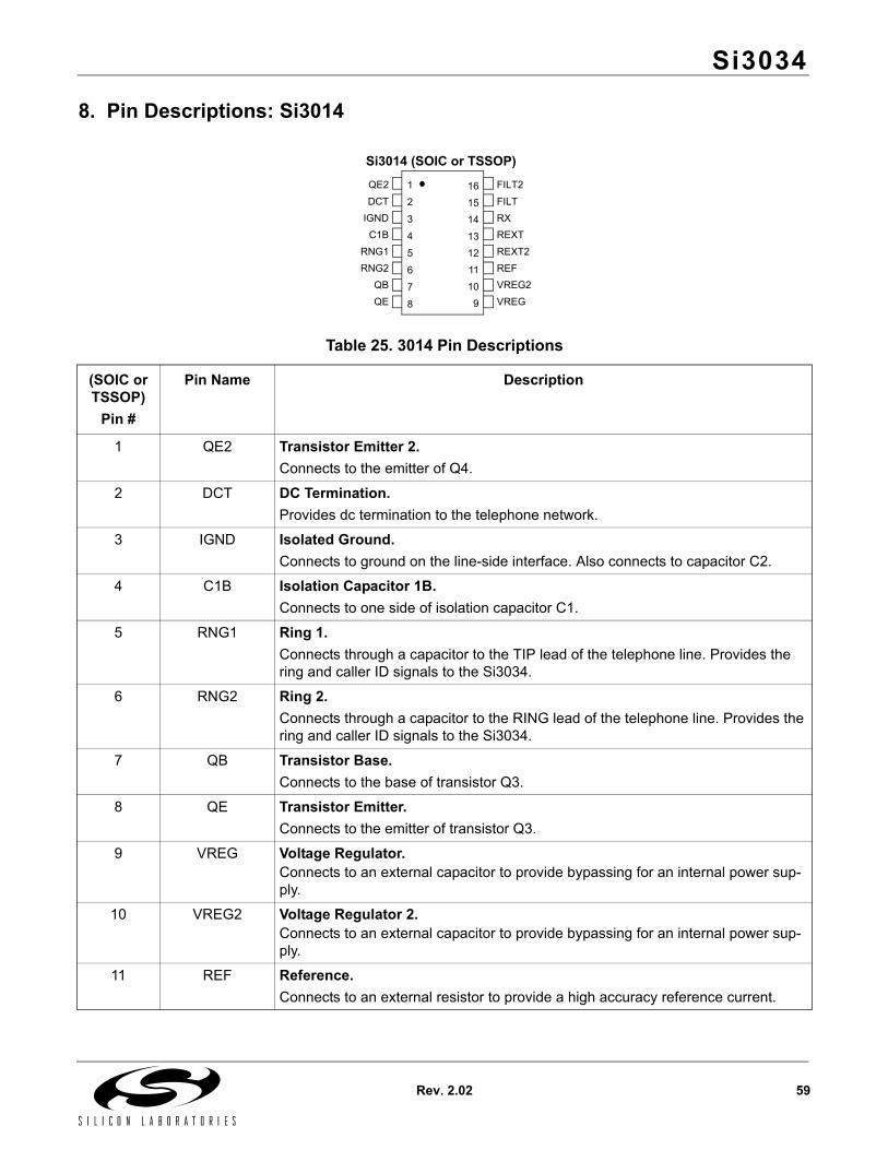
Si3034
Rev. 2.02 59
8. Pin Descriptions: Si3014
Table 25. 3014 Pin Descriptions
(SOIC or TSSOP)
Pin #
Pin Name Description
1 QE2 Transistor Emitter 2.Connects to the emitter of Q4.
2 DCT DC Termination.Provides dc termination to the telephone network.
3 IGND Isolated Ground.Connects to ground on the line-side interface. Also connects to capacitor C2.
4 C1B Isolation Capacitor 1B.Connects to one side of isolation capacitor C1.
5 RNG1 Ring 1.Connects through a capacitor to the TIP lead of the telephone line. Provides the ring and caller ID signals to the Si3034.
6 RNG2 Ring 2.Connects through a capacitor to the RING lead of the telephone line. Provides the ring and caller ID signals to the Si3034.
7 QB Transistor Base.Connects to the base of transistor Q3.
8 QE Transistor Emitter.Connects to the emitter of transistor Q3.
9 VREG Voltage Regulator.Connects to an external capacitor to provide bypassing for an internal power sup-ply.
10 VREG2 Voltage Regulator 2.Connects to an external capacitor to provide bypassing for an internal power sup-ply.
11 REF Reference.Connects to an external resistor to provide a high accuracy reference current.
1
2
3
4
5
6
7
8 9
1011
1213
16
1514
QE2DCT
IGNDC1B
RNG1RNG2
QBQE
FILT2FILTRXREXTREXT2REFVREG2VREG
Si3014 (SOIC or TSSOP)

Si3034
60 Rev. 2.02
12 REXT2 External Resistor 2.Sets the complex ac termination impedance.
13 REXT External Resistor.Sets the real ac termination impedance.
14 RX Receive Input.Serves as the receive side input from the telephone network.
15 FILT Filter.Provides filtering for the dc termination circuits.
16 FILT2 Filter 2.Provides filtering for the bias circuits.
Table 25. 3014 Pin Descriptions (Continued)
(SOIC or TSSOP)
Pin #
Pin Name Description

Si3034
Rev. 2.02 61
9. Ordering Guide1,2,3
System Side
Part Number Package Lead-Free Temp Range
Si3021-X-ZS# SOIC-16 Yes 0 to 70 °C
Si3021-X-ZT# TSSOP-16 Yes 0 to 70 °C
Si3021-X-FS# SOIC-16 Yes 0 to 70 °C
Si3021-X-FT# TSSOP-16 Yes 0 to 70 °C
Line Side
Part Number Package Lead-Free Temp Range
Si3014-X-FS SOIC-16 Yes 0 to 70 °C
Si3014-X-FT TSSOP-16 Yes 0 to 70 °C
Notes:1. “X” denotes product revision.2. Add an “R” at the end of the device to denote tape and reel option; 2500 quantity per reel.3. “#” denotes customer-specific bond ID.

Si3034
62 Rev. 2.02
10. Package Outline: 16-Pin SOICFigure 36 illustrates the package details for the Si3014 and the Si2493 16-pin packaging option. Table 26 lists thevalues for the dimensions shown in the illustration.
Figure 36. 16-pin Small Outline Integrated Circuit (SOIC) Package
Table 26. Package Diagram Dimensions
Symbol MillimetersMin Max
A 1.35 1.75A1 .10 .25B .33 .51C .19 .25D 9.80 10.00E 3.80 4.00e 1.27 BSCH 5.80 6.20h .25 .50L .40 1.27γ 0.10θ 0º 8º
aaa 0.25bbb 0.25
E H
A1
B
C
h
L
θ
e
See Detail F
Detail F
A
16 9
81
D
Seating Plane γ
-B-Bbbb
-A-
BACaaa
-C-
Approximate device weight is 152 mg.

Si3034
Rev. 2.02 63
11. Package Outline: 16-Pin TSSOPFigure 37 illustrates the package details for the Si3024 and Si3014. Table 27 lists the values for the dimensionsshown in the illustration.
Figure 37. 16-Pin Thin Small Shrink Outline Package (TSSOP)
Table 27. Package Diagram Dimensions
Symbol MillimetersMin Nom Max
A — — 1.20A1 0.05 — 0.15b 0.19 — 0.30c 0.09 — 0.20D 4.90 5.00 5.10e 0.65 BSCE 6.40 BSCE1 4.30 4.40 4.50L 0.45 0.60 0.75
θ1 0° — 8°bbb 0.10ddd 0.20
L
θ1
c
D
A1
A
b
E1 E
e
See Detail G
Detail G
1 2 3ddd C B A
A
C
16
bbb C B AM
B

Si3034
64 Rev. 2.02
DOCUMENT CHANGE LISTRevision 1.0 to Revision 1.1
Typical Application Circuit was updated.C24, C25 value changed from 470 pF to 1000 pF and C31, C32 were added in Table 13 and Table 14. In Table 14, the tolerance was also changed from 20% to 10%.Power Supply Voltage, Analog maximum changed from 4.75 V to 5.00 V in Table 4.Last paragraph updated in “31 Power Management”text section.
Revision 1.1 to Revision 1.2Added TSSOP pinout and package drawing.Added note to Table 2.Amended numbers in Table 3.Amended numbers in Table 4.Amended note #4 in Table 5.Amended numbers in Table 7.Replaced Figure 4.Updated Analog Output text.Added China to Table 16.Added “On-Chip Charge Pump” section.Added “DC Termination Considerations” section.Figure 16, “Typical Application Circuit for the Dual Design Si3034 and Si3035,” on page 15 updated.Table 13, “Global Component Values,” on page 16 (BOM) updated.Table 14, “FCC Component Values—Si3035 Chipset,” on page 17 (BOM) updated.
Revision 1.2 to Revision 2.0Updated schematic and BOM.Added Appendix B.Corrected transmit frequency response specification to 0 Hz typical.Updated “27 Overload Detection” section text concerning CTR21 mode.Removed CTRO bit (Register 19, bit 7).
Revision 2.0 to Revision 2.01Table 16 updated.“56 Appendix B—CISPR22 Compliance” updated.The “Ringer Impedance Network” figure and the “Component Values—Optional Ringer Impedance Network” table were deleted from the “24 Ringer Impedance”section as well as a paragraph discussing Czech Republic designs.The “Dongle Applications Circuit” figure was deleted.
Revision 2.01 to Revision 2.02Added support for lead-free/RoHS-compliant packages and updated lead-free part numbers (page 1 features and Ordering Guide).Updated footnotes in BOM (no changes in schematic or BOM component values).Updated Table 16 on page 19 and footnote 2 to list several countries adopting TBR21.Updated SOIC and TSSOP package drawings and dimensions tables.

Si3034
Rev. 2.02 65
NOTES:
Si3034
66 Rev. 2.02
CONTACT INFORMATIONSilicon Laboratories Inc.4635 Boston LaneAustin, TX 78735Tel: 1+(512) 416-8500Fax: 1+(512) 416-9669Toll Free: 1+(877) 444-3032Email: [email protected]: www.silabs.com
Silicon Laboratories and Silicon Labs are trademarks of Silicon Laboratories Inc.Other products or brandnames mentioned herein are trademarks or registered trademarks of their respective holders.
The information in this document is believed to be accurate in all respects at the time of publication but is subject to change without notice. Silicon Laboratories assumes no responsibility for errors and omissions, and disclaims responsibility for any consequences resulting from the use of information included herein. Additionally, Silicon Laboratories assumes no responsibility for the functioning of undescribed features or parameters. Silicon Laboratories reserves the right to make changes without further notice. Silicon Laboratories makes no warranty, rep-resentation or guarantee regarding the suitability of its products for any particular purpose, nor does Silicon Laboratories assume any liability arising out of the application or use of any product or circuit, and specifically disclaims any and all liability, including without limitation conse-quential or incidental damages. Silicon Laboratories products are not designed, intended, or authorized for use in applications intended to support or sustain life, or for any other application in which the failure of the Silicon Laboratories product could create a situation where per-sonal injury or death may occur. Should Buyer purchase or use Silicon Laboratories products for any such unintended or unauthorized ap-plication, Buyer shall indemnify and hold Silicon Laboratories harmless against all claims and damages.