Embed Size (px)
Citation preview

Tutorial - ADOPT 2014 1
Department of Microelectronics and Information Technology
KTH, Royal Institute of Technology
Integrated Devices and Circuits
Royal Institute of Technology (KTH)
Si-based materials for
photonics and electronics
Henry H. Radamson

Tutorial - ADOPT 2014 2
Outline of this tutorial
* It begins with an introduction why photonics is merging more with electronics.
Shall we have a common roadmap of both electronics and photonics? More than Moore
* Main objective of this tutorial is to present a monolithic solution when Si photonics conqueres, in long term, the
interconnections between circuit-to-cirtuit & chip-to-chip.
How detection and lasing occur in Si-based materials
* The bandstructure of Si-based materials
* Intersubband lasing (Si-based materaisl have indirect bandgap) but transitions occurs within the conduction and
valence band states)
* Interband lasing (make Si-based materials to have direct bandgap )
* Down scaling of CMOS
Which type of strain, which design, and how to maximize strain in channel
* Future materials graphene or two dimentional crystals

Tutorial - ADOPT 2014 3
IEEE Spectrum Aug. 2002
We need to develop different photonic components beside the CMOS part
Emerging of photonic and electronic world
Electronics
Data processing
Photonics
Data communication

Tutorial - ADOPT 2014 4
New areas for Si photonics and electronics
Adavantages: Silicon is transparent for light above 1.1µm and has a very high refractive
index, that allows for tight light confinement in a core of about 0.1µm2 and high level of integration. Integrated photonic structures based on SOI wafers can be fabricated using existing microelectronic technology.
Drawbacks: Indirect bandgap, making light generation difficult.

Tutorial - ADOPT 2014 5
Today’s technology landscape of CMOS
The landscape of the technology is now on nanostructures
The number of transistors in a chip is doubled every two years
5 http://www.legitreviews.com/article/1082/1 http://hexus.net/tech/news
Technology node evolution: non-selective growth to
selective epitaxy, substrate size, metal gate,
silicide. But 22nm node and beyond : 2D to 3D (Tri-
gate) design

Tutorial - ADOPT 2014 6
The Silicon Photonics Technology Leti – STMicroelectronics, 2010
Silicon photonics roadmap

Tutorial - ADOPT 2014 7
How about a roadmap for both electronics
and photonics?

Tutorial - ADOPT 2014 8
Strain engineering and bandstructure of
group IV alloys
Tutorial - ADOPT 2014 9
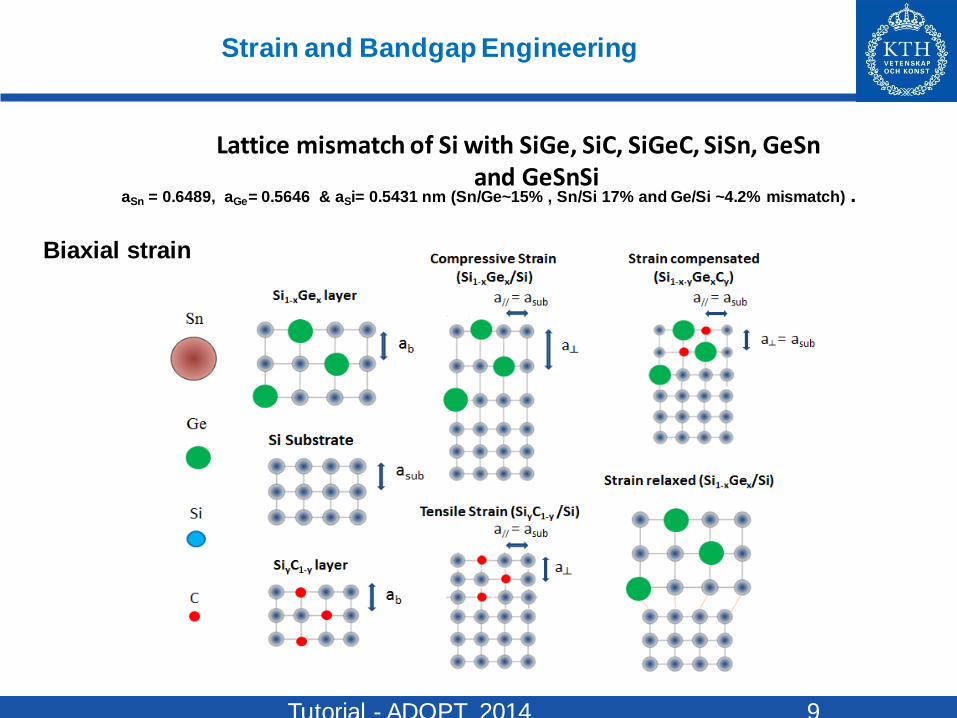
Strain and Bandgap Engineering
Lattice mismatch of Si with SiGe, SiC, SiGeC, SiSn, GeSn and GeSnSi
aSn = 0.6489, aGe= 0.5646 & aSi= 0.5431 nm (Sn/Ge~15% , Sn/Si 17% and Ge/Si ~4.2% mismatch) .
Biaxial strain

Tutorial - ADOPT 2014 10
Strain engineering in group IV alloys
An alloy has different strain and bandgap
The layers can be integrated in advanced photonic device

Tutorial - ADOPT 2014 11
Strain generation
- Epitaxy: Biaxial strain
(mismatched heterostructures)
-Processing: Biaxial strain
(Silicide & thermal cycling)
Stressor materials: Uniaxial strain
(nitride, SiGe & Si1-yCy)
http://www.tf.uni-kiel.de Liu et al. Appl. Phys. Lett. 87, 011110 2005

Tutorial - ADOPT 2014 12
Inducing stress of > 1 GPa in pMOSFETs
Tuning SiN stress from highly tensile to compressive stress in LPCVD and PECVD.
The mechanical property of nitride layers is
determined by controlling the gas phase dissociation of Silane, Amonia and gases
in a plasma environment
These nitride layers can be grown on embedded SiGe layers.
The induced stress is additive to the induced SiGe stress.
Arghavani et al. IEEE Electron Device Letters, V27 (2006) 114

Tutorial - ADOPT 2014 13
Critical thickness of strained-SiGe layers
All strained alloys e.g. SiGe or GeSn are grown in meta-stable region and they relax after a
certain critical thickness.
Radamson et al. Physica Scripta T101 (2002) 42.
X
X
No strain relaxation
is observed for
selectively grown
layers
X
Silicon Substrate
Selective epi Oxide
SiGe

Tutorial - ADOPT 2014 14
- Low-temperature solid-source MBE/CVD
- Gas precursors: Ge2H6 and SnD4 (expensive and not stable for long time), SnCl4 (cheap and reliable gas source), Si2H6, Si3H8
-Ge growth 300-600 °C
- GeSn growth directly on Si or Ge at low temperatures (e.g. 250-350 °C)
Growth of Ge, GeSi, GeSn and SiGeSn materials
J. Kouvetakis et al, IEEE Photonics Journal, 2, 924, 2010 H. Radamson et al, ECS conference (2012)
A revolutionary developement in production of new gas precursors for CVD
Lower temperatures required for higher Sn content
High quality GeSn(Si) layers have been reported

Tutorial - ADOPT 2014 15
GeSn alloys’ properties
J. Mathews et al. Appl. Phys. Lett. 97, 221912 (2010) 221912-1

Tutorial - ADOPT 2014 16
Si Ge
Ge has nearly direct bandgap of 0.85 eV
Bandstructure of Si and Ge
Tutorial - ADOPT 2014 17
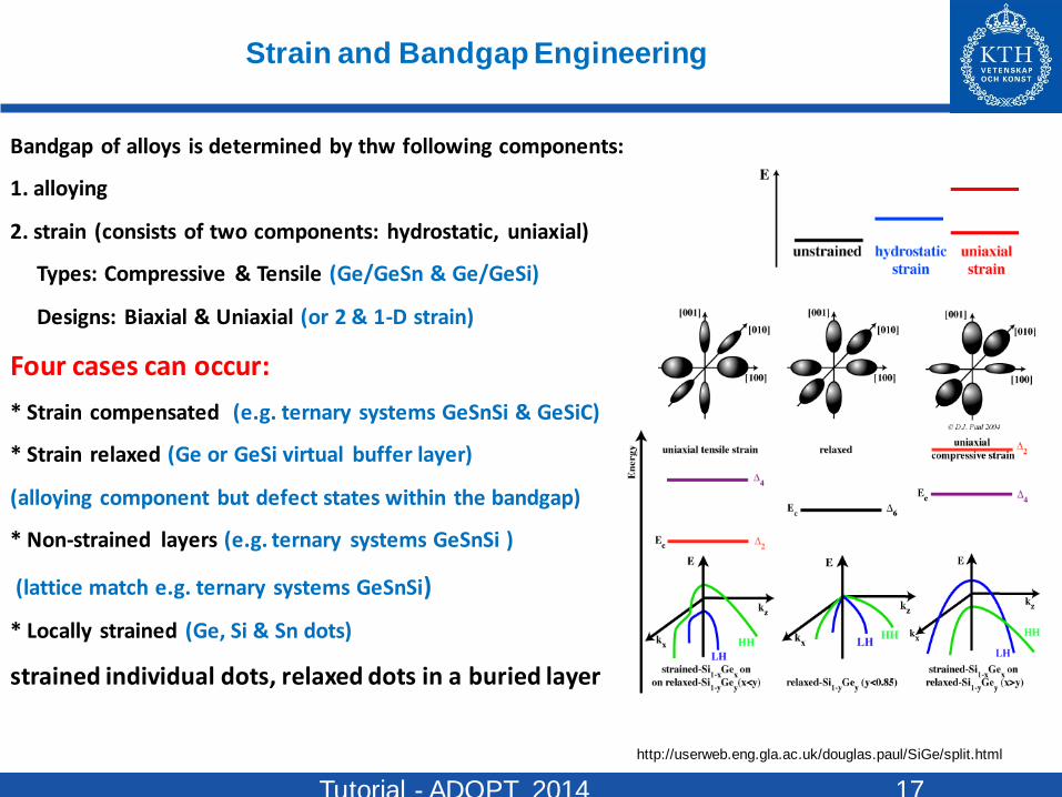
Bandgap of alloys is determined by thw following components:
1. alloying
2. strain (consists of two components: hydrostatic, uniaxial)
Types: Compressive & Tensile (Ge/GeSn & Ge/GeSi)
Designs: Biaxial & Uniaxial (or 2 & 1-D strain)
Four cases can occur:
* Strain compensated (e.g. ternary systems GeSnSi & GeSiC)
* Strain relaxed (Ge or GeSi virtual buffer layer)
(alloying component but defect states within the bandgap)
* Non-strained layers (e.g. ternary systems GeSnSi )
(lattice match e.g. ternary systems GeSnSi)
* Locally strained (Ge, Si & Sn dots)
strained individual dots, relaxed dots in a buried layer
Strain and Bandgap Engineering
http://userweb.eng.gla.ac.uk/douglas.paul/SiGe/split.html

Tutorial - ADOPT 2014 18
GeSn alloy and its application
Sun et al, Opt Quant Electron (2012) 44:563–573
This provides the possibility for monolithic integration of photonic devices on Si
- Possible material system for photonic
application:
- GeSn alloy system
- GeSnSi alloy system
- strained Ge on GeSn or SiGeSn for direct band
gap (via tensile strain)
- Unstrained Ge (or SiGe) on SiGeSn for
intersubband applications – quantum cascade
lasers (QCLs)
- SiSn alloy on GeSn for communication
wavelengths (1.3 mm – 1.55 mm)
Transition of indirect-bandgap to a direct bandgap with Sn content 6-8%

Tutorial - ADOPT 2014 19
Decoupling of electronic structure and lattice parameter:
Direct-gap values tunable between 0.8 and 1.4 eV, in GeSiSn alloys epitaxially grown on Ge-buffered Si, as a function of the combined Si + Sn fraction x. Dots are experimental values and solid line is a fit to:
E0(X)=E0Ge+AX+BX2 , A=1.70+0.42, B=-1.62+0.96
V. R. D’Costa, et al., Phys. Rev. Lett. 102, 107403, 2009; J. Kouvetakis, et al., IEEE Photonics Journal, 2, 924, 2010.
Tunable optical gap at a fixed lattice constant - Ge1-x(Si4Sn)x

Tutorial - ADOPT 2014 20
alloys can be applied as an alternative to other matched
infrared systems e.g.
SiGeSn material may have the same
lattice match but different bandgaps
Si-Ge-Sn ternary system templates for integration of III-V
compounds with Si
A lattice-matched system with tuning bandgap is ideal for multicolor detector
applications like target discrimination, gas leakage detection and enviromental
sensing.

Tutorial - ADOPT 2014 21
Calculated band diagram of a Ge0.65Si0.15Sn0.20–Ge
strained layer structure showing the indirect to
direct crossover (EcG lower than EcL). Holes are
localized in the lh band due to tensile strain in Ge.
This is of interest for interband quantum well lasers,
Band-edge diagrams for lattice-
matched, SiGeSn–Ge hetero-
structures. Electrons and holes are
confined in Ge layer (type I). This is
of interest for intersubband, quantum
cascade lasers,
Laser design for Ge
G. Sun, et al., Appl. Phys. Lett., 90, 251105, 2007. S.-W. Chang, S. L. Chuang, IEEE J. Quantum Electronics. 43, 249, 2007.

Tutorial - ADOPT 2014 22
Group IV materials for photonic detectors

Tutorial - ADOPT 2014 23
Ge is absorbant of light
- High absorption for wavelengths of interest
- CMOS compatible
Si does not absorb/detect and can guide light (λ>1.1um, IR) .
Mario Panicca, Si Photonics, Photodector announcement, Intel devoper forum

Tutorial - ADOPT 2014 24
PiN Ge detectors
Si Substrate
p-doped Si
p-doped Ge
Intrinsic Ge
n-doped Ge NiGe +
TiW/Al
Contact
NiGe +
TiW/Al
Contact
PIN Ge structure
Ge detectors for 0.86-0.6 eV

Tutorial - ADOPT 2014 25
Ge/Slot-Waveguide integration Solution
Selectively grown Ge photodetectors on Si
Back coupling as waveguide integration
Waveguide
Stack
High-k
ALD Slots
Incident Light
M. M.Naiini et al, ISDRS 2013

Tutorial - ADOPT 2014 26
Ge/Slot-Waveguide integration Solution
Simulated waveguide/detector coupling
3% feedback in case of perfect side wall
Negligible feedback due to roughness
0.5 μm
6.8 μm
M. M.Naiini et al, ISDRS 2013

Tutorial - ADOPT 2014 27
Tensile Ge for NIR detectors
GeSn is defected but Ge cap layer has remarkably higher epi-quality
Strain-relaxed Ge1-xSnx / tensile Ge
The strain in Ge is determined by Sn content in the buffer layer.
HRRLM of a GeSn/Ge structure grown on Si substrate at 290 ºC.
A. Jamshidi,, Surface and Coatings Technology, 2013.

Tutorial - ADOPT 2014 28
Photodetection (PD)– photoconductive devices
V. R. D’Costa, et al., Semicond. Sci. Technol. 24, 115006, 2009
Ge has a sharp direct gap absorption edge at 0.80 eV (1549 nm) at room
temperature, outside the range of the so-called L-band (1560–1620 nm) utilized
by ultrahigh-speed optical networks. Ge PD response at 1620 nm is just 10% of
that at 1540 nm. This can be overcome by using the relaxed Ge0.98Sn0.02 alloy.

Tutorial - ADOPT 2014 29
Photodetection – p-i-n diode
J. Mathews, et al., Appl. Phys. Lett. 95, 133506, 2009
… while a p-i-n photodetector based on the same material can cover the
whole O – U range of optical telecommunication bands.
Si photonic technology is leading the way to a new generation of telecommunications

Tutorial - ADOPT 2014 30
025% strain in Ge: 1.5 µm Ti & annealed @
800 C for 5 min to obtain C54 TiSi2
Liu et al. Appl. Phys. Lett. 87, 011110 2005
Ge p-i-n photodetectors

Tutorial - ADOPT 2014 31
Lasing and design in group IV materials

Tutorial - ADOPT 2014 32
0.25% tensile strain, the difference between Γ and L valleys is decreased to 115 meV
Ge: direct gap material at 1.7% tensile strain: Eg=~0.4 eV: λ =3000 nm
Compensate: 7.6×10¹⁹/cm3
Jifeng Liu et al. OPTICS EXPRESS, Vol. 15, No. 18, P 11273
Tensile Ge/GeSn systems
Optically pumped
lasing demonstrated

Tutorial - ADOPT 2014 33
Intersubband laser in regions:
Near infrared (1-2µm) or middle infrared (2-20 µm): Si1-xGex/Si (x=25-50% where
ΔEv is in range of 205-420 meV) is for 5-20 µm laser.
Si-based Intersubband lasers
The emission wavelength depends ΔEv or ΔEc
which controls the subband energy separations.
Three- and two-coupled quatum wells (3CQW and 2CQW)
Wavefunction engineering: barrier height, selecting
well and barrier widths: adjust the subband energies and spatial overlap of wavefunctions into
the neighboring subbands. Carriers are confined in
z-direction and are unconfined in x- and y-direction.
Photon & phonon scattering in 3-subband group IV
laser pumped at subband 3. q32 & q21 are phonon momenta and ħω=phonon energy. The overlap of
wavefunctions has to be engineered that T3>T2
occurs. A desired overlap of wavefunctions 3 & 2 by adjusting the barrier width. The unpolar group IV has
advantage over III-V polar deformation potential.

Tutorial - ADOPT 2014 34
p-i-p (n-i-n) first, a doped multi-layer Bragg mirror, which may be λ/4
layers of Si and ZnS, on SOI film. The active, undoped three Si CMQW
is grown on that mirror.
Near Infrared lasers
Near-infrared subband laser: deep wells (large band offset which must be above ~1.2 hw (620-1240 meV)
Proposed heterostructures: Si (QW)/ZnS (barrier), Si/SiO2, ...
R. Soref et al., Superlattices and Microstructure, Vol. 23 (1998) 427

Tutorial - ADOPT 2014 35
Si1−xGex /Si cascade
ex. Si0.75Ge0:25/Si
E(hh1)= 53 meV,
E (hh2)=83 meV,
E(lh1) = 99 meV,
E(lh2)= 142 meV,
E(hh3)=152 meV.
6–8µm wavelength Si0:6Ge0:4

Tutorial - ADOPT 2014 36
Intersubband lasers (QCLs)
G. Sun et al., Appl. Phys. Lett., 90, 251105, 2007
Strain-free Ge/SiGeSn system for quantum cascade lasers based on the
L-valley intersubband transitions (indirect band gap is irrelevant here,
and using L-valley instead of G may even offer some advantages).

Tutorial - ADOPT 2014 37
Strained Ge interband lasers
G.-E. Chang, S.-W. Chang, S. L. Chuang, Opt. Express 17, 11246, 2009 S.-W. Chang, S. L. Chuang, IEEE J. Quantum El. 43, 249, 2007,

Tutorial - ADOPT 2014 38
Strained Ge interband lasers
Surface carrier densities of the G- and L-
conduction valleys as a function of the
injected carrier density. The large density
of states of L-subbands, and four
equivalent L-valleys, lead to a significant accumulation in L-subbands.
Band line-up in Ge/SiGeSn quantum
well structure. Due to tensile strain in
the well, there is only one hole
subband, and it is LH.

Tutorial - ADOPT 2014 39
Double heterostructure lasers
G. Sun et al Opt Quant Electron (2012) 44:563–573
Cooling is needed

Tutorial - ADOPT 2014 40
G. Sun et al Opt Quant Electron (2012) 44:563–573
Multi-quantum well lasers

Tutorial - ADOPT 2014 41
Synthesis of GeSnSi layers
Thermodynamically favorable
for Si and Sn atoms in Ge
H. Radamson et al, ECS conference (2012)
Similar behavior
for P- and B-doped
GeSn

Tutorial - ADOPT 2014 42
Evolution of CMOS techology

Tutorial - ADOPT 2014 43
Mark Bohr (Intel Senior Fellow) & Kaizad Mistry (Program manager), Intel’s revolutionary 22 nm technology, Intel 2011
MOSFET’s evolution
The limit is expected to be at the gate length of around 5 nm because of the too huge off-
leakage current in the entire chip
In order to suppress the off-leakage current, Tri-Gate is the most promising
solution

Tutorial - ADOPT 2014 44
Tri-Gate transistors provide a
steeper sub-threshold slope that reduces leakage current
22 nm Tri-Gate transistors can operate
at lower voltage
with good performance, reducing
active power by >50%
Advantages of Tri-Gate transistors
Mark Bohr (Intel Senior Fellow) & Kaizad Mistry (Program manager), Intel’s revolutionary 22 nm technology, Intel 2011

Tutorial - ADOPT 2014 45
Sub-22nm technology is 3D growth
45
Nanowires, Si/fins

Tutorial - ADOPT 2014 46
Downscaling (critical parameters)
The downscaling of MOSFETs improves IDSAT, and decreases CGate and VD per generation node and when
VD is modified then the gate delay and energy-delay product are also improved.
IDSAT = saturation drive
current,
CGate = gate load,
VD = supply voltage.
when the transistor dimensions are scaled down → increased speed and lower power consumption of digital MOS circuits
Power supply voltage (Vdd), Threshold
voltage (Vt) and gate oxide thickness
(tox) vs. CMOS channel length
Danny Rittman et al., http://www.tayden.com/publications/CMOS%20Nanometer%20Designs%20Scaling%20Limited.pdf

Tutorial - ADOPT 2014 47
Evolution of MOSFETs
SiGe in S/D has
been increased
constantly
Silicides

Tutorial - ADOPT 2014 48
Mobility of SiGe (some data of biaxial strain)
The improvement of mobility of SiGe layers in biaxial strain is due to decrease of scattering
Mobility values in uniaxial strain is always higher than biaxial strain

Tutorial - ADOPT 2014 49
Selective epitaxy growth issue (Pattern dependency)
49
SiGe layer profile (thickness, Ge & dopant content) in the openings of the same chip, chip-to-chip and wafer-to-wafer varies due to the exposed Si coverage (size, density) and architecture (oxide & nitride) of the wafer.
Exposed Si coverage in a chip [%]
What is pattern dependency?

Tutorial - ADOPT 2014 50
New materials and possibilities for channel materials
Ashwin Ramasubramaniam et al, Nano Lett. 2011, 11, 1070–1075
Synthesize two graphene sheets and tune the bandgap

Tutorial - ADOPT 2014 51
Tuning bandgap of Graphene
Ashwin Ramasubramaniam et al, Nano Lett. 2011, 11, 1070–1075
Graphene as channel material for MOSFETs for 10 nm node?

Tutorial - ADOPT 2014 52
Single-layer MoS2 is interesting as a semiconducting analogue of graphene, which does not posses a bandgap in its
pristine form. Bandgaps up to 400 meV have been introduced by quantum-mechanical confinement.
Radisavljevic et al, Nature Nanotechnology Vol 6, (2011) 147
Transistors demonstrate current on/off ratio exceeding 1 × 10⁸ and mobility of ~200 cm2 V−1 s−1,
comparable to the mobility achieved in thin Si films or graphene nanoribbons
Alternative materials: GeS, GeSe
New materials and possibilities for channel materials
Tutorial - ADOPT 2014 53
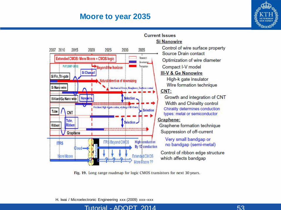
Moore to year 2035
H. Iwai / Microelectronic Engineering xxx (2009) xxx–xxx

Tutorial - ADOPT 2014 54
Merging photonics and electronics,
3D design

Tutorial - ADOPT 2014 55
Detectors, modulators, …
To manufacture laser from group IV material is on-going research: GeSn is a
promising material
(Alt. III-V on Si)
Merging photonics and electronics

Tutorial - ADOPT 2014 56
I. Jonak-Auer, Proc. of SPIE Vol. 8431, 843115 (2012) SPIE
New integation concept
0.35 µm CMOS
Responsivity value: 0.57A/W at a wavelength of 675nm
One extra mask: PIN is manufactured

Tutorial - ADOPT 2014 57
57
3%
5% 1%
0%
8%
10%
Our solutions for pattern dependency of selective epitaxy
6%
8% 7%
5%
9%
10%
10%
10%
10%
5%
5%
5%
5%
8%
10%
10%
10%
10%
5%
5%
5%
5%
8%
7
%
7
%
7
%
7
%
7
%
7
% 10%
1) Uniform pattern distribution
2) Insert dummy features
Pattern dependency is caused by
nonuniform gas consumption in
advanced chip design Two solutions to make a uniform
gas consumption over a chip
An example of a test chip with different exposed Si coverages
This mask design will provide
uniform transistor structure

Tutorial - ADOPT 2014 58
Future 3D integration
Integrated CMOS and laser
R. Soref, IEEE JOURNAL OF SELECTED TOPICS IN QUANTUM ELECTRONICS, VOL. 12, (2006)
3D SOI substrates will be an option for
advanced integration of photonic and electronic circuits

Tutorial - ADOPT 2014 59
Si photonics has a bright future

Tutorial - ADOPT 2014 60
Thank you for your attention