Embed Size (px)
Citation preview

MATLAB SIMULATION OF SINGLE PHASE SHUNT ACTIVE POWER FILTER AND DEVELOPMENT OF
EXPERIMENTAL SET UP
SHYAMSUNDAR JENA (110EE0199)
Department of Electrical Engineering,
National Institute of Technology, Rourkela

2 | P a g e
MATLAB SIMULATION OF SINGLE PHASE SHUNT ACTIVE POWER FILTER AND DEVELOPMENT OF
EXPERIMENTAL SET UP
A thesis submitted in partial fulfilment of the requirements for the degree of
Bachelor of Technology in “Electrical Engineering”
By
SHYAMSUNDAR JENA (110EE0199)
Under the Supervision of
Prof. K.B.Mohanty
Department of Electrical Engineering
National Institute of Technology Rourkela-769008 (ODISHA)
May-2014

i | P a g e
DEPARTMENT OF ELECTRICAL ENGINEERING
NATIONAL INSTITUTE OF TECHNOLOGY, ROURKELA
ODISHA, INDIA-769008
CERTIFICATE
This is to certify that the thesis report titled “MATLAB Simulation of Single Phase Shunt
Active Power Filter and Development of Experimental Set up”, submitted to the National
Institute of Technology, Rourkela by Mr. Shyamsundar Jena, Roll No: 110EE0199 for the
award of Bachelor of Technology in Electrical Engineering is a bona fide record of research
work carried out by him under my supervision and guidance.
The candidate has fulfilled all the prescribed requirements.
The thesis report which is based on candidate’s own work has not been submitted elsewhere
for a degree/diploma.
In my opinion, the thesis report is of standard required for the award of a Bachelor of
Technology in Electrical Engineering.
Prof. K.B. Mohanty
Supervisor
Department of Electrical Engineering
National Institute of Technology
Rourkela – 769 008 (ODISHA)

ii | P a g e
ACKNOWLEDGEMENTS Fore mostly, I would like to express my sincere gratitude to my supervisor Prof. K.B.
Mohanty, for his patience, motivation and financial support for the project work. I sincerely
appreciate and value his esteem guidance and encouragement from the beginning till the end
of my thesis.
I wish to express my sincere gratitude to Prof.A.K Panda (HOD) for approving the budget to
purchase some of the components required for the project work. I am very much thankful to
Mr.Maheswar Mahato, and Gobardhan Rana for assisting me in developing the experimental
setup.
I would also like to thank Prof. P.K Ray, Prof. B.Chitti Babu, Prof. Gopalkrishna and other
faculty members of Electrical Engineering Department, NIT Rourkela for their
encouragement, support and motivation.
Last but not the least; I would also like to thank my parents, sister, brother and all well-
wishers for their co-operation, sacrifice and motivational moral support which bring me to
this level.
Shyamsundar Jena

iii | P a g e
DEDICATED TO
ALMIGHTY…

iv | P a g e
ABSTRACT
This project work presents a single phase shunt active power filter based on synchronous
detection method. Due to wide use of nonlinear single phase power electronic devices in low
voltage side has increased harmonic pollution in the power system to the larger extent.
Improving power quality has become the biggest challenge for electrical engineers. A single
phase shunt active power filter was modeled in MATLAB/SIMULINK using hysteresis
current controller and triangular current controller. Simulation results are presented to
demonstrate performance of single phase shunt active power filter during presence of
nonlinear load. An experimental setup is established to validate the simulation result.

v | P a g e
TABLE OF CONTENTS
CERTIFICATE i
ACKNOWLGEMENT iii
ABSTRACT iv
TABLE OF CONTENETS v
LIST OF FIGURES viii
ABBREVIATIONS AND ACRONYMS ix
CHAPTER-1
INTRODUCTION
1.1 BACKGROUND 2
1.2 MOTIVATION OF PROJECT WORK 3
1.3 OBJECTIVES OF PROJECT WORK 4
CHAPTER-2
HARMONICS AND HARMONIC COMPENSATION SCHEMES
2.1.SOURCES OF HARMONICS 7
2.2.HARMONIC REDUCTION AND REACTIVE POWER 7
2.3.COMPENSATION TECHNIQUES 7
2.3.1. PASSIVE FILTER 7
2.3.2. ACTIVE POWER FILTER 9
CHAPTER-3
LITERATURE REVIEW OF SHUNT ACTIVE POWER FILTER
3.1 SHUNT ACTIVE POWER FILTER 11
3.2 SYNCHRONOUS DETECTION METHOD 11
3.3 SYNCHRONOUS REFERENCE FRAME ALGORITHM 12

vi | P a g e
3.4 PEAK DETECTION METHOD 13
CHAPTER-4
MODELING AND SIMULATION
4.1 MATHEMATICAL MODELLING 15
4.2 SINGLE PHASE SHUNT ACTIVE POWER FILTER 16
4.3 DESIGN OF CONTROLLER 16
4.3.1 OUTER DC LINK VOLTAGE CONTROLLER 17
4.3.2 HYSTERESIS CURRENT CONTROLLER 17
4.3.3 TRIANGULAR CARRIER CURRENT CONTROLLER 19
4.4 SIMULATION RESULTS 20
CHAPTER-5
EXPERIMENTAL SETUP DESCRIPTION
5.1 INTRODUCTION 31
5.2 EXPERIMENTAL SETUP 31
5.2.1 SINGLE PHASE VARIAC 32
5.2.2 IGBT BASED INVERTER 32
5.2.3 SINGLE PHASE RECTIFIER 33
5.2.4 SIGNAL CONDITIONING CIRCUIT 33
5.2.4.1 CURRENT SENSOR 34
5.2.4.2 VOLTAGE SENSOR 36
5.2.4.3 GATE DRIVER 39
5.2.4.4 FILTER INDUCTOR 40
CHAPTER-6
CONCLUSION
6.1 CONCLUSION 42

vii | P a g e
REFERENCES 43
APPENDIX-A 44
APPENDIX-B 45
APPENDIX-C 46
APPENDIX-D 47

viii | P a g e
LIST OF FIGURES
1.1: Block diagram for active power filter connected system 12
2.1 Block diagram for passive filter connected power system 16
4.1: Control algorithm for generation of reference current and gate pulse 21
4.2 Power circuit diagram of single phase APF connected system 22
4.3: DC link PI controller 23
4.4: Hysteresis logic 24
4.5: Hysteresis Controller implemented in MATLAB SIMULINK 25
4.6: Triangular Carrier Controller implemented in MATLAB SIMULINK 26
4.7: Source voltage 27
4.8: Zoomed version of source voltage 27
4.9: Source current & load current 27
4.10: Zoomed version of source current & load current 27
4.11: Filter current 28
4.12: Zoomed version of filter current 28
4.13: Tracking of DC link voltage 28
4.14: Zoomed version of tracking of DC link voltage 28
4.15: Phase relationship between source voltage and source current 29
4.16: Zoomed version of phase relationship between source voltage and source current 29
4.17: Reactive power compensation 29
4.18: Gate pulses waveform 30
4.19: Zoomed version of gate pulse waveform 30
4.20: THD of source current before use of active power filter 30
4.21: THD of source current after use of active power filter 31
4.22: Source voltage 31
4.23: Zoomed version of source voltage 31
4.24: Source current & load current 32
4.25: Zoomed version of source current & load current 32
4.26: Filter current 32
4.27: Zoomed version of filter current 33
4.28: Tracking of DC link voltage 33
4.29: Phase relationship between source voltage and source current 33
4.30: Zoomed version of phase relationship between source voltage and source current 34

ix | P a g e
4.31: Reactive power compensation 34
4.32: Zoomed version of gate pulse waveform 34
4.33: THD of source current before use of active power filter 35
4.34: THD of source current after use of active power filter 35
5.1: Entire experimental set up 36
5.2: Single phase variac 36
5.3: DC link capacitor 36
5.4: IGBT based VSI 37
5.6: Working principle of current sensor 39
5.7: Schematics of current sensor 39
5.8: Current sensor card 39
5.9: Linear relationship between sensor output voltage and input current 41
5.10: Voltage sensor card 42
5.11: Working principle of voltage sensor 42
5.12: Linear relationship between sensor output voltage and input current 43
5.13: Gate driver output 44
5.14: Schematics of gate driver circuit 45
5.15: Gate driver card 45

x | P a g e
ABBREVIATIONS AND ACRONYMS
SCR - Silicon Controlled Rectifier
IGBT - Insulated Gate Bipolar Transistor
MOSFET - Metal Oxide Semiconductor Field Effect Transistor
APF - Active Power Filter
PCC - Point of Common Coupling
SMPS - Switched Mode Power Supply
AC - Alternating Current
DC - Direct Current
PI - Proportional Integral
THD - Total Harmonic Distortion
PWM - Pulse Width Modulation
VSI - Voltage Source Inverter
SAPF - Shunt Active Power Filter
HVDC - High Voltage Direct Current

1 | P a g e
CHAPTER 1
Introduction
2 | P a g e
1.1 Background
Power quality improvement has become a major research topic in modern power distribution
system. Nearly twenty years ago most of the loads used by the industries and consumers were
passive and linear in nature, with a lesser number of non-linear loads thus having less impact
on the power system. With the arrival of semiconductor and power electronic devices and
their easier controllability have caused wide use of non-linear loads such as chopper, inverter
switched mode power supply, rectifier, etc. The power handled by modern power electronics
devices like silicon controlled rectifier (SCR), Insulated gate bipolar transistor (IGBT),
power diode, Metal oxide semiconductor field effect transistor (MOSFET) are very large,
which promotes their industrial as well as domestic applications. With addition to that various
power electronic devices are used to increase the efficiencies and power factor of wind, solar,
and other non-conventional sources of energy. While the advantages of using above devices
are certainly good but there are some demerits of such excessive use of power electronic
devices. The use of above semiconductor devices is responsible for harmonic and reactive
power disturbances. The harmonics and reactive power are the cause various problem which
includes overheating of transformers, excessive neutral current, distortion of feeder voltage,
low power factor, damages to power electronic devices and malfunction of sensitive
equipment [1]. To eliminate the harmonics in the power system, active power filters (APF)
are installed at PCC. APF injects compensating current at PCC to cancel out the harmonics
and to make source current sinusoidal. By installation of APF, harmonic pollution as well as
low power factor in the power system can be improved. Though APFs are widely used in
three phase system, by little modification in the control strategy it can be implemented in the
single phase system, thus harmonic pollution can be
reduced at low voltage system.

3 | P a g e
Fig.1 Block diagram for active power filter connected system
1.2 Motivation of Project Work
Harmonic pollution in low voltage side is more prominent compare to high voltage side due
wide use of nonlinear single phase loads (Computers, Battery charger, Printers etc.), which is
unacceptable. It is a huge challenge to nullify the undesirable current harmonics and
compensate the reactive power requirement in the power system. The performances of
traditional practices (use of LC filter) are not acceptable due to its serious drawbacks as
discussed. The shunt APF provides encouraging results compare to traditional one based up
on appropriate control algorithms. The control strategy play a key role for better dynamic
performances of the APF. Most of the existing control schemes used for active power filter
involve three phase quantity. By little modification, those control strategies can be used for
single phase system. The synchronous detection method is used for three phase active power
filter; this project work proves that synchronous detection method can be used for single
phase active power filter which involves lesser complexities compare to that of instantaneous
reactive power algorithm.

4 | P a g e
1.3 Objectives of Project Work
The objectives of this project are
To discuss effect of harmonics arising due to nonlinear load
To study different control strategies already proposed for modeling of 3 phase shunt
active power filter
To model and simulate single phase active power filter in MATLAB/SIMULINK
environment
Design of hystesrsis current controller
Design of triangular carrier current controller
Experimental validation of simulation work
1.4 Organization of Thesis
The thesis is divided into 6 chapters including the chapter introduction. Each chapter is
different from each other and is described with necessary theory and diagrams to understand
it.
Chapter 2 deals with harmonics, causes of harmonics and the effect of harmonics on power
system. Various schemes used to compensate harmonic is also discussed in this chapter.
Previously passive filter was used to eliminate harmonics but due to their poor dynamic
performances they are replaced by active power filter. The modern trend of eliminating
harmonic is to use active power filter.
Chapter 3 presents literature review of shunt active power filter and its control strategy.
Shunt active power filter nullify the effect of harmonics by injecting complementary
component of harmonics being generated by nonlinear loads. The dynamic performances of
shunt active power filter depend upon the control strategy adopted to generate the reference
current. In this chapter various control algorithms like synchronous detection method,
synchronous reference frame algorithm and peak detection method are discussed.

5 | P a g e
Chapter 4 presents mathematical modeling and simulation of single phase shunt active
power filter. From the knowledge of load voltage and load current, power consumed by
nonlinear load is calculated. By knowing load power, reference source current is generated.
This reference current is compared with actual source current and the error signal is
processed through a current controller to generate gate pulses for VSI. This chapter also deals
with design of controllers like hysteresis current controller and triangular current carrier
controller. Various simulation results are given for both the controller to observe their
performances.
Chapter 5 deals with description of various hardware components required to establish
experimental setup for single phase shunt active power. It also deals with calibration of
current sensor and voltage sensor.
Chapter 6 gives comparative analysis of the simulation results between hysteresis controller
based active power filter and triangular carrier controller based active power filter.

6 | P a g e
CHAPTER 2
Harmonics and Harmonic Compensation Schemes

7 | P a g e
2.1 Source of Harmonics
The term ‘Harmonic’ refers to a component with a frequency that is an integral multiple of
the fundamental frequency. Harmonics in power system arises due to wide use of nonlinear
loads. The major causes of current and voltage harmonics are due to energy conversion
techniques and control involved in the power electronic devices such as rectifier, chopper,
cyclo-converter etc. Energy conversion devices like voltage controller devices of motor,
HVDC power converters, battery-charging systems, power factor improvement devices,
traction, static-var compensators, direct energy devices-fuel cells, wind and solar-powered
dc/ac converters, storage batteries which require dc/ac power converters, control of heating
elements cause harmonic pollution in power system [7].
2.2 Harmonic Reduction and Reactive Power Compensation Techniques The harmonic filter connected to AC system has two objectives
1. To minimize the effect of harmonic voltage and current in the power system below an
acceptable level.
2. To compensate the reactive power required by the loads.
Two type of filters used for the above purposes which are
Passive filter
Active power filter
2.2.1 Passive Filter The passive filter requires resistors, inductors, and capacitors and they do not depend upon
any type of external power source. By proper selection of L and C, they are tuned to bypass a
particular harmonic component. Multiple numbers of passive filters are connected in parallel
to nullify higher order of harmonics as shown in Fig.1. Though passive filters were widely
used as harmonic improvement and reactive power compensation devices in the power
distribution system, their performances is not satisfactory due to following reasons:

8 | P a g e
A separate filter is necessary for each harmonic frequency.
Passive filter must be designed in considering with current provided by nonlinear
load.
Source impedance affects the compensation characteristics of LC filters.
When the content of harmonics in the AC line increases, the filter will be loaded.
Frequency variation of AC source and tolerances in the filter components will affect
the compensation characteristics of LC filters. If the system frequency varies in wide
range, components required for attaining tuned frequency become impracticable.
Fig.2 Block diagram for passive filter connected power system
With the above mentioned disadvantages the passive filter are less frequently used compared
to active power filter. The practice of using the active power filter is the future trend of
harmonic improvement in power distribution system because of its excellent dynamic
characteristics. A flexible and handy solution to harmonic problem is provided by active
power filters. Presently they are based on PWM converters and connected to low and medium
voltage distribution system either in shunt or series.

9 | P a g e
2.2.2 Active Power Filter
Between different technical option available to eliminate harmonics and compensate reactive
power in the power system, active power filter [11] system has been proved to be most
prominent one. Active power filters (APF) are constructed using both passive and active
elements. For their operation they need external power source. Presently available APFs are
basically of pulse width modulated inverters (current source or voltage source).Current fed
PWM inverter act as non-sinusoidal current source to cancel out the harmonic current
produced by nonlinear load. Current fed PWM based APF’s use is limited to low power
application. Voltage source inverter (VSI) is the most popular one for implementing active
power filtering. VSI based APFs have high power rating and lower switching frequency.
They are connected to AC mains through coupling reactors.
Active power filter can be classified into three categories as per their
connection to the PCC, namely
1. Shunt active power filter
2. Series active power filter
3. Hybrid active power filter
But shunt active power filter is widely used due to its simpler construction and robustness. A
brief idea about shunt active power filter and its control schemes are discussed in the next
chapter.

10 | P a g e
CHAPTER 3
Literature Review of Shunt Active Power Filter
11 | P a g e
3.1 Shunt Active Power Filter
SAPFs are widely used in the power system to compensate reactive power and current
harmonics. It can also play the role of static VAR generator in the power system for
improving and stabilizing the voltage profile. Shunt active power filter compensate current
harmonic by injecting complementary current that of produced by non-linear load. Shunt
active power filter acts as a current source by introducing the harmonic components created
by the load but phase shift by 180.Consequently, the current harmonic component present in
the load current got cancelled and the source current remain sinusoidal and in phase with the
respective phase to neutral voltage. By the use of proper control scheme, APF can also
improve system power factor. Thus, by the effect of active power filter, voltage sources see
the nonlinear load simply as resistor.
However the performances of SAPF largely depend on the
control strategy which is responsible for generating complementary harmonic current to
cancel out the current harmonics present in the load current. Various control strategies [2]-[6]
for SAPF are discussed below
3.2 Synchronous Detection Method Synchronous theory [4] can work efficiently under both balanced and unbalanced condition
of source as well as load as the reference current are calculated considering the magnitude of
each phase voltage separately. Current is distributed equally among three phases, to estimate
the three phase compensating current to be provided by the active filter. Two assumptions are
taken into consideration while calculating three phase reference currents i.e. Source voltage is
not distorted and Peak magnitude of source currents are balanced after compensation as given
in (1)
bsysrs III (1)

12 | P a g e
Where rsI , ysI and bsI are the amplitudes of three phase source current after compensating. The
real power consumed by the load can be calculated as
Lr
r y b Ly
Lb
ip v v v i
i
(2)
Where, rv , yv and bv are load voltages and Lri , Lyi and Lbi are load current. The active power p is
sent through a low pass filter to obtain its average value dcP .Then the active power is split into
three phases as follows (3)
dc rr
dc yy
dc bb
P EPE
P EP
EP EP
E
(3)
Where rE , yE and bE are the amplitudes of the source voltages re , ye and be . E is the
algebraic sum of rE , yE and bE .The desired reference current can be calculated as (4)
2*
2*
2*
2
2
2
b
bbbl
y
yyyl
r
rrrl
EPeI
EPe
I
EPeI
(4)
3.3 Synchronous Reference Frame Algorithm
This method is quite similar to instantaneous reactive power theory method. The important
features of this algorithm [5] is that it require only load current for generating reference
current and hence source disturbances or voltage distortion have no effect on the
performances of active power filter system. As this method involves synchronous frame of

13 | P a g e
reference, a separate PLL is required for each phase to synchronize reference current with its
corresponding phase to neutral voltage.
3.4 Peak Detection Method
In this method [5] distorted load current is filtered to extract fundamental component of load
current. After obtaining fundamental component of load current, its phase is shifted by 180.If
this current is added with distorted load current, it will give the waveform of current which is
required to compensate only the harmonic distortion present in the load current. In order to
compensate the reactive power required by the load, extracted fundamental component of
load current has to be synchronized with its corresponding phase to neutral voltage.

14 | P a g e
CHAPTER 4
Modelling and Simulation
15 | P a g e
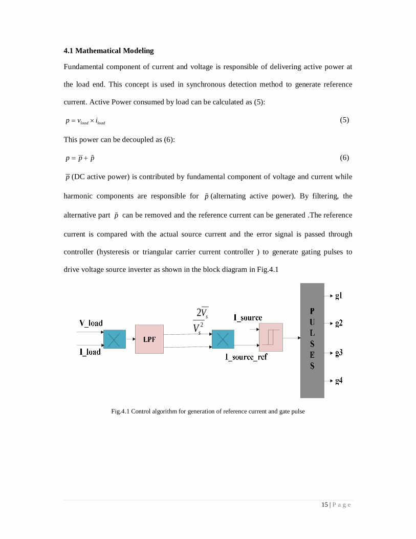
4.1 Mathematical Modeling
Fundamental component of current and voltage is responsible of delivering active power at
the load end. This concept is used in synchronous detection method to generate reference
current. Active Power consumed by load can be calculated as (5):
load loadp v i (5)
This power can be decoupled as (6):
p p p (6)
p (DC active power) is contributed by fundamental component of voltage and current while
harmonic components are responsible for p (alternating active power). By filtering, the
alternative part p can be removed and the reference current can be generated .The reference
current is compared with the actual source current and the error signal is passed through
controller (hysteresis or triangular carrier current controller ) to generate gating pulses to
drive voltage source inverter as shown in the block diagram in Fig.4.1
22
sVsV
Fig.4.1 Control algorithm for generation of reference current and gate pulse

16 | P a g e
4.2 Single Phase Shunt Active Power Filter
Single phase shunt active filter consists of IGBT/MOSFET based inverter shunted with DC
link capacitor. It is connected to point of common coupling through AC link reactor. The
power circuit diagram of single phase shunt active power filter connected system is shown in
the Fig.4.2 .It consists of single phase supply utility, single phase bridge rectifier, single
phase IGBT based voltage source inverter, controller and load.
Fig.4.2 Power circuit diagram of single phase APF connected system
4.3 Design of Controller
The heart of the active power filter system is its controller. Proper control scheme enables
active power filter to carry out harmonic elimination as well as reactive power compensation.
The controller of shunt active power filter is divided into two parts i.e.
1. Inner current control loop
2. Outer DC link voltage control loop
17 | P a g e
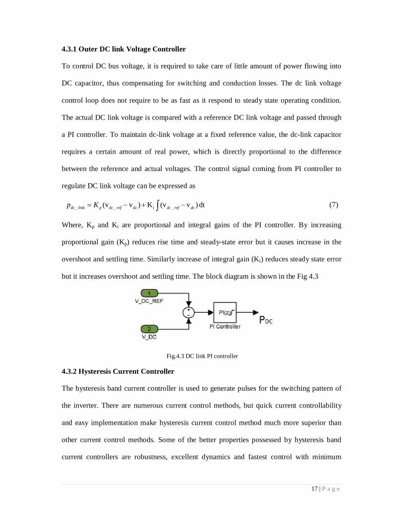
4.3.1 Outer DC link Voltage Controller
To control DC bus voltage, it is required to take care of little amount of power flowing into
DC capacitor, thus compensating for switching and conduction losses. The dc link voltage
control loop does not require to be as fast as it respond to steady state operating condition.
The actual DC link voltage is compared with a reference DC link voltage and passed through
a PI controller. To maintain dc-link voltage at a fixed reference value, the dc-link capacitor
requires a certain amount of real power, which is directly proportional to the difference
between the reference and actual voltages. The control signal coming from PI controller to
regulate DC link voltage can be expressed as
_ _ _(v v ) K (v v ) dtdc link p dc ref dc i dc ref dcp K (7)
Where, Kp and Ki are proportional and integral gains of the PI controller. By increasing
proportional gain (Kp) reduces rise time and steady-state error but it causes increase in the
overshoot and settling time. Similarly increase of integral gain (Ki) reduces steady state error
but it increases overshoot and settling time. The block diagram is shown in the Fig 4.3
Fig.4.3 DC link PI controller
4.3.2 Hysteresis Current Controller
The hysteresis band current controller is used to generate pulses for the switching pattern of
the inverter. There are numerous current control methods, but quick current controllability
and easy implementation make hysteresis current control method much more superior than
other current control methods. Some of the better properties possessed by hysteresis band
current controllers are robustness, excellent dynamics and fastest control with minimum
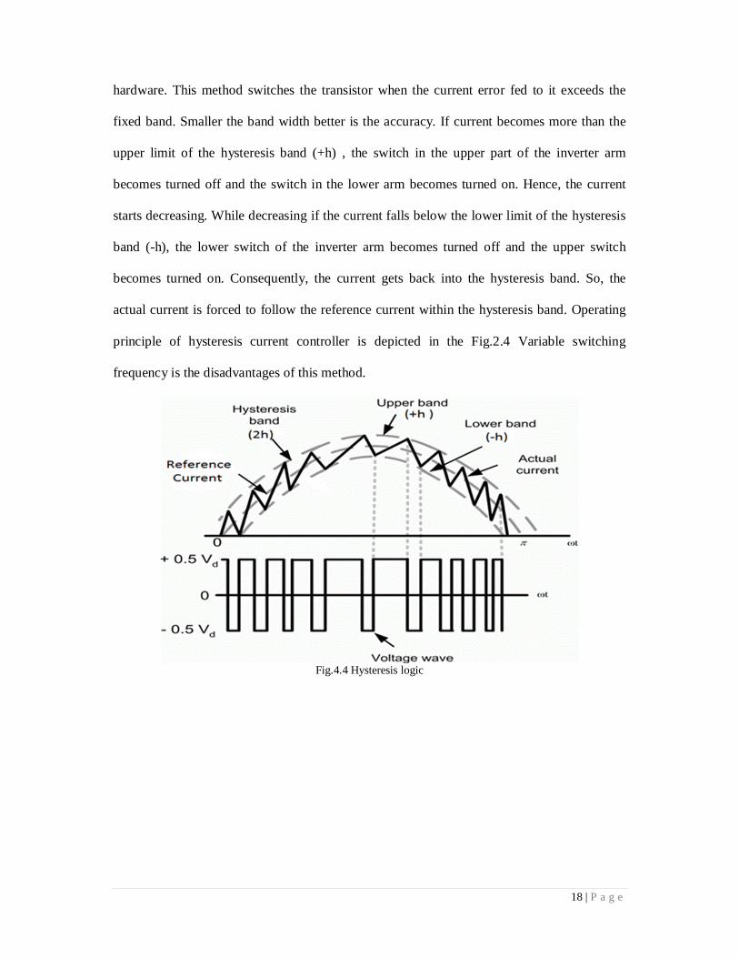
18 | P a g e
hardware. This method switches the transistor when the current error fed to it exceeds the
fixed band. Smaller the band width better is the accuracy. If current becomes more than the
upper limit of the hysteresis band (+h) , the switch in the upper part of the inverter arm
becomes turned off and the switch in the lower arm becomes turned on. Hence, the current
starts decreasing. While decreasing if the current falls below the lower limit of the hysteresis
band (-h), the lower switch of the inverter arm becomes turned off and the upper switch
becomes turned on. Consequently, the current gets back into the hysteresis band. So, the
actual current is forced to follow the reference current within the hysteresis band. Operating
principle of hysteresis current controller is depicted in the Fig.2.4 Variable switching
frequency is the disadvantages of this method.
Fig.4.4 Hysteresis logic

19 | P a g e
Fig.4.5 Hysteresis Controller implemented in MATLAB SIMULINK
4.3.2 Triangular Carrier Current Controller
In this method [5] the current error is compared with the fixed frequency and fixed amplitude
of triangular carrier wave. The current error is passed through a proportional integral (PI)
controller before comparison with the triangular carrier wave. When the carrier wave
(Triangular wave) is smaller than the error signal, the gate signal is positive and upper switch
will be turned on and lower switch will become turned off. When the carrier wave
(Triangular wave) is larger than the error signal, the gate signal is zero, and upper switch will
become turned off and lower switch will become turned on. This results in a gate pulse with
variable width. Increasing proportional gain (Kp) decreases rise time and steady-state error
but increases the overshoot and settling time. Increasing integral gain (Ki) reduces steady
state error but increases overshoot and settling time. The frequency of the carrier wave
determines the switching frequency. As switching frequency is known, switching losses can
be predicted. Block diagram of triangular carrier current controller is depicted in the Fig.4.6.

20 | P a g e
Fig 4.6 Triangular Carrier Controller implemented in MATLAB SIMULINK
4.4 Simulation Results Single phase shunt active power filter system is simulated in MATLAB/SIMULINK
environment. Various parameter used for simulation is given in the Table 4.1.The model was
run for 0.2 second without connecting active power filter to PCC of power circuit and then
active power filter was connected to the power circuit. At the time connecting active power
filter to the power circuit, there is large increase in source current. This large current is
known as inrush current which arises due to initially uncharged capacitor at the inverter end.
It can be minimized by the use of thermistor in series with DC link capacitor.
Sl No. Simulation Parameters Ratings 1 Source Voltage 230V(r.m.s) 2 Source Inductance 1mH 3 Single Phase Bridge Rectifier --- 4 R-L Load 10 ohm,50 mH 5 Filter Inductance 5 mH 6 IGBT/Diodes --- 7 DC Link Capacitor 4700 uF 8 DC Link Ref.Voltage 400V 9 Sampling Frequency (Ts) 1e-4
10 DC Link PI Controller Kp=25, Ki=20 11 Hysteresis Current controller Hysteresis Band=0.1 12 Triangular Carrier Current Controller Switching Freq=1e+4
Sampling Frequency=1e+5
Table 4.1

21 | P a g e
4.5 Simulation Result for Hysteresis Current Controller Based APF
Fig.4.7 Source voltage
Fig.4.8 Zoomed version of source voltage (0.6 Sec to 0.7 Sec)
Fig.4.9 Source current & load current
Fig.4.10 Zoomed version of source current & load current (0.6 Sec to 0.7 Sec)

22 | P a g e
Fig.4.11 Filter current
Fig.4.12 Zoomed version of filter current (0.6 Sec to 0.7 Sec)
Fig.4.13 Tracking of DC link voltage
Fig.4.14 Zoomed version of tracking of DC link voltage (0.6 Sec to 0.7 Sec)

23 | P a g e
Fig.4.15 Phase relationship between source voltage and source current
Fig.4.16 Zoomed version of phase relationship between source voltage and source current (0.6 sec to 0.7 sec)
Fig.4.17 Reactive power compensation (Though y ordinate unit is in watt, for reactive power it will be treated as
VAR)

24 | P a g e
Fig.4.18 Gate pulses waveform
Fig.4.19 Zoomed version of gate pulses waveform (0.6 sec to 0.6015 sec)
Fig.4.20 THD of source current before use of active power filter

25 | P a g e
Fig.4.21 THD of source current before use of active power filter
4.6 Simulation Result for Triangular Carrier Current Controller Based APF
Fig.4.22 Source voltage
Fig.4.23 Zoomed version of source voltage (0.6 Sec to 0.7 Sec)

26 | P a g e
Fig.4.24 Source current & load current
Fig.4.25 Zoomed version of source current & load current (0.6 Sec to 0.7 Sec)
Fig.4.26 Filter current

27 | P a g e
Fig.4.27 Zoomed version of filter current (0.6 Sec to 0.7 Sec)
Fig.4.28 Tracking of DC link voltage
Fig.4.29 Phase relationship between source voltage and source current
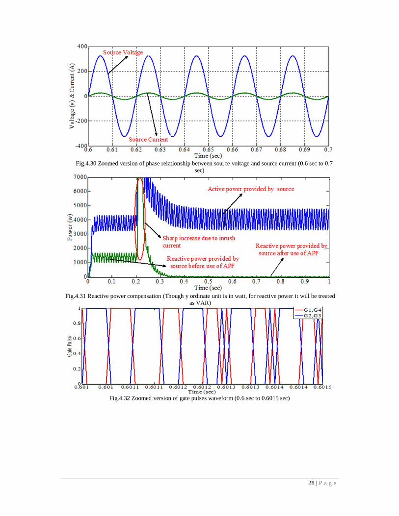
28 | P a g e
Fig.4.30 Zoomed version of phase relationship between source voltage and source current (0.6 sec to 0.7
sec)
Fig.4.31 Reactive power compensation (Though y ordinate unit is in watt, for reactive power it will be treated
as VAR)
Fig.4.32 Zoomed version of gate pulses waveform (0.6 sec to 0.6015 sec)

29 | P a g e
Fig.4.33 THD of source current before use of active power filter
Fig.4.34 THD of source current before use of active power filter

30 | P a g e
CHAPTER 5
Experimental Setup Description

31 | P a g e
5.1 INTRODUCTION A set up is developed to test the effectiveness of both circuit topology and control strategy.
Detail descriptions of individual hardware component, their circuit topology and output result
are presented in this chapter.
5.2 EXPERIMENTAL SETUP
Fig.5.1 Entire experimental set up
The entire hardware set up used for experimental purposes can be categorized into
1. Single phase Variac
2. IGBT based inverter
3. Single phase rectifier
4. Signal conditioning circuit
5. Filter inductor
32 | P a g e
6. Source inductor
7. DC link capacitor
8. R-L load
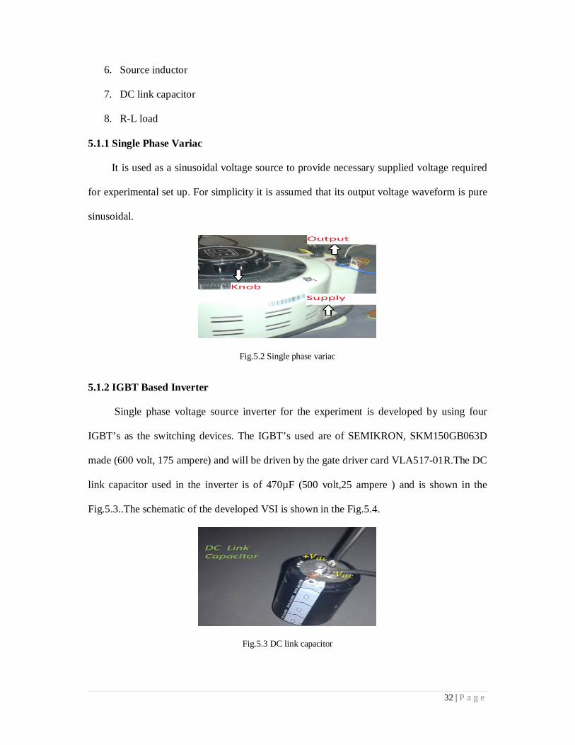
5.1.1 Single Phase Variac
It is used as a sinusoidal voltage source to provide necessary supplied voltage required
for experimental set up. For simplicity it is assumed that its output voltage waveform is pure
sinusoidal.
Fig.5.2 Single phase variac
5.1.2 IGBT Based Inverter
Single phase voltage source inverter for the experiment is developed by using four
IGBT’s as the switching devices. The IGBT’s used are of SEMIKRON, SKM150GB063D
made (600 volt, 175 ampere) and will be driven by the gate driver card VLA517-01R.The DC
link capacitor used in the inverter is of 470µF (500 volt,25 ampere ) and is shown in the
Fig.5.3..The schematic of the developed VSI is shown in the Fig.5.4.
Fig.5.3 DC link capacitor

33 | P a g e
Fig.5.4 IGBT based VSI
5.1.3 Single Phase Rectifier
The combination of single phase rectifier and R-L load is used as a nonlinear load to create
harmonics in the source current. The power diode used to construct Rectifier Bridge is of 15
ampere, 500 volt.
Fig.5.4 IGBT based VSI
5.1.4 Signal Conditioning Circuit
In this section the description of the different sensors and the gate driver card for the IGBT’s
of the VSI are described.
34 | P a g e
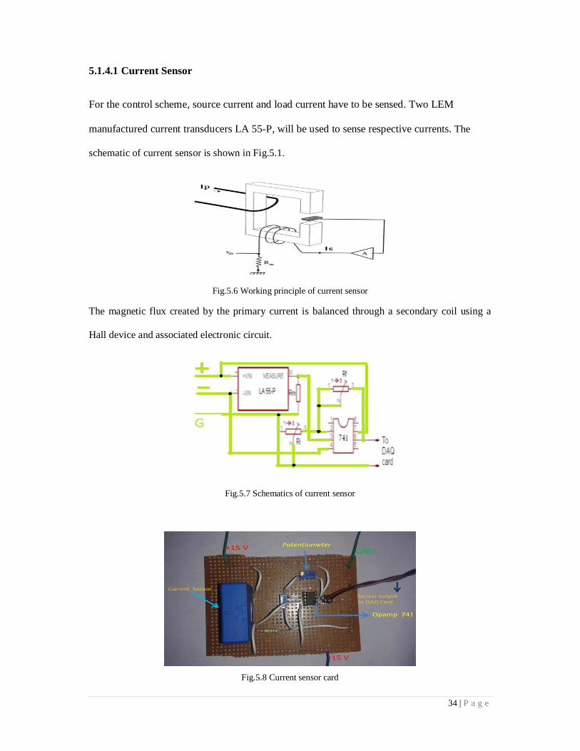
5.1.4.1 Current Sensor
For the control scheme, source current and load current have to be sensed. Two LEM
manufactured current transducers LA 55-P, will be used to sense respective currents. The
schematic of current sensor is shown in Fig.5.1.
Fig.5.6 Working principle of current sensor
The magnetic flux created by the primary current is balanced through a secondary coil using a
Hall device and associated electronic circuit.
Fig.5.7 Schematics of current sensor
Fig.5.8 Current sensor card

35 | P a g e
The number of secondary turns (Ns) is 1000 and the maximum value of secondary current (Is)
is 50mA. Primary current (Ip) is the current that is to be measured. The magnetic flux created
by the primary current is balanced through a secondary coil using a Hall device and
associated electronic circuit. The relation given by Equation (5.1) holds true during operation.
Np×Ip=Ns×Is (5.1)
Where, Np is number of primary turns. In the experiment, Np = 1, thus a primary current up
to 50A can be safely measured. Since the turn ratio is constant, the secondary current is an
exact representation of the primary current. The output signal is the voltage drop on the
resistance Rm caused by the secondary current. A 100Ω resistance is selected as Rm. This
output signal needs to be scaled within the analog input limits (-10V to +10V) of data
acquisition card, which is done by a non-inverting opamp configuration. Two variable
resistances, Ri and Rf, are used to select a proper gain. The current sensor and opamp both
require ±15V supply for their operation which is provided by DC power supply module. The
complete circuit is shown in Fig.5.7. It is then calibrated to find the exact relation between
input current and output voltage. Two current sensor cards are required for sensing
1. Source current
2. Load current
Current sensor card for measuring source current
Current sensor card for source current measurement is designed for measuring alternating
current of maximum of 10A (r.m.s). The sensor is calibrated such that sensor output is 2V for
1A of input current to be sensed. The curve fitting formula for current sensor card for
measuring panel voltage is computed using MATLAB as
푣 = 2.189 × 푖 − 0.1207 (5.2)

36 | P a g e
Current sensor card for measuring load current
Current sensor card for source load measurement was designed for measuring alternating
current of maximum of 40A (r.m.s). The sensor is calibrated such that sensor output is 1V for
2A of input current to be sensed. The curve fitting formula for current sensor card for
measuring panel voltage is computed using MATLAB as
푣 = 2.192 × 푖 + 0.1081 (5.3)
The curve obtained from curve fitting tool of MATLAB for calibrating the current sensor
(source) is shown in the Fig.5.9.
Fig.5.9 Linear relationship between sensor output voltage and input current
5.1.4.2 Voltage Sensor
Source voltage, load voltage dc-link capacitor voltages are to be sensed accurately for proper
operation of controller. Three LEM manufactured voltage transducer LV 25-P are used to
sense respective voltages. The complete specification of voltage sensor is provided in
Appendix A. The design note for voltage sensor card and calibrations for acquiring correct
sensed voltages are given in Appendix B. The voltage sensor card fabricated on printed
circuit board is shown in Fig.5.10.
0 1 2 3 4 5 60
5
10
Current (A)
Sens
or V
olta
ge (
V)
37 | P a g e
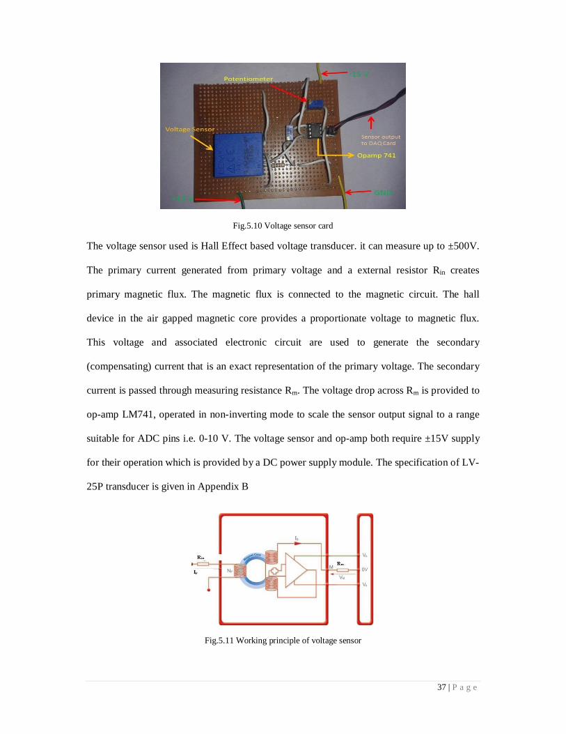
Fig.5.10 Voltage sensor card
The voltage sensor used is Hall Effect based voltage transducer. it can measure up to ±500V.
The primary current generated from primary voltage and a external resistor Rin creates
primary magnetic flux. The magnetic flux is connected to the magnetic circuit. The hall
device in the air gapped magnetic core provides a proportionate voltage to magnetic flux.
This voltage and associated electronic circuit are used to generate the secondary
(compensating) current that is an exact representation of the primary voltage. The secondary
current is passed through measuring resistance Rm. The voltage drop across Rm is provided to
op-amp LM741, operated in non-inverting mode to scale the sensor output signal to a range
suitable for ADC pins i.e. 0-10 V. The voltage sensor and op-amp both require ±15V supply
for their operation which is provided by a DC power supply module. The specification of LV-
25P transducer is given in Appendix B
Fig.5.11 Working principle of voltage sensor

38 | P a g e
Three voltage sensor cards are required for sensing:
1. Source voltage
2. Load voltage
3. DC link capacitor voltage
All three voltage sensor card for were designed for measuring maximum of 500V (470V).
The value of input resistance placed at the positive terminal of voltage transducer considering
optimum accuracy at nominal primary current of 10mA, was 50KΩ/5W. A resistance of
65KΩ/5W was placed. The sensor is calibrated such that sensor output is 1V for 10V of input
voltage to be sensed. The curve fitting formulas for three voltage sensors are computed as:
For source voltage sensor, 푣 = 0.0923 × 푣 + 0.2380 (5.4)
For load voltage sensor, 푣 = 0.0904 × 푣 + 0.2541 (5.5)
For DC link voltage sensor, 푣 = 0.0941 × 푣 _ + 0.3541 (5.6)
The curve obtained from curve fitting tool of MATLAB for calibrating the voltage sensor
(load) is shown in the Fig.5.12.
Fig.5.12 Linear relationship between sensor output voltage and input current
10 20 30 40 50 60 70 80 90 100
2
4
6
8
10
Voltage (V)
Sens
or O
utpu
t Vol
tage
(V)

39 | P a g e
5.1.4.3 Gate Driver
High performance FUJI’s hybrid IGBT driver IC, VLA517-01R will be used to provide the
necessary driving signals to the IGBT across the gate emitter terminals. This hybrid IC is a
circuit designed for driving n-channel IGBT modules. An optocoupler is used in this chip to
provide the required isolation between the signal side of the chip and the power side. The
input to the chip is a digital signal of +5V as logic high and 0V as logic low and the
corresponding outputs are +15V and -5V which is shown in Fig.5.13.
Fig.5.13 Gate driver output
Output of this chip is connected through a proper gate series resistance (Rg=25Ω) across the
gate emitter terminals of the corresponding IGBT, which is to be driven. The input logic
signal given to the chip should be capable of driving a current of 10mA for the satisfactory
operation of this chip. The pin description and details of the IC VLA517-01R are given in the
Appendix C. The circuit diagram implemented in the present work for the IGBT driver is
shown in Fig.5.14. The complete gate driver circuit is fabricated and is shown in Fig.5.15.

40 | P a g e
Fig.5.14 Schematics of gate driver circuit
Fig.5.15 Gate driver card
5.1.6 Filter Inductor
The purpose of using filter inductor is to eliminate very high frequency component from filter
injected current and to limit the inrush current to protect IGBT .

41 | P a g e
CHAPTER 6
Conclusion and Future Activity

42 | P a g e
6.1 CONCLUSION From MATLAB/SIMULINK simulation of hysteresis current controller based active power
filter, it is found that THD of source current is reduced to 1.86 % from 29.86 % after use of
filter. Reactive power required by nonlinear load is completely compensated by active power
filter (APF) and power factor at source end becomes almost unity. By using triangular carrier
current controller based active power filter, it is found that THD of source current is reduced
to 3.64 % from 29.38 % and reactive power is also completely compensated and power
factor is also found to be unity at the source end. The higher THD value in compensated
source current of triangular carrier current controller based active power filter is due to low
switching frequency of carrier wave which I cannot increase beyond 10 KHz due to
computational limitation of my computer.
Due to late delivery of some
components and lack of availability of proper interfacing devices at the last moment, I could
not able to run the complete setup to validate the simulation result. In future I will try to
validate the simulation works through experimentation.

43 | P a g e
REFERENCES:
[1] Grady, W. Mack, and Surya Santoso. "Understanding power system harmonics." IEEE
Power Engineering Review 21.11 (2001): 8-11.
[2] Morán, Luis A., et al. "Using active power filters to improve power quality." 5th Brazilian Power Electronics Conference. 1999.
[3] Jou, H-L. "Performance comparison of the three-phase active-power-filter algorithms." IEE Proceedings-generation, Transmission and Distribution 142.6 (1995): 646-652.
[4] Chin Chen, Chin-Lin, and Chin E. Lin. "An active filter for an unbalanced three-phase system using the synchronous detection method." Electric power systems research 36.3 (1996): 157-161.
[5] Rashid, Muhammad H. "Power electronics handbook, 2007." [6] Seifossadat, S. G., et al. "Quality improvement of shunt active power filter, using
optimized tuned harmonic passive filters." Power Electronics, Electrical Drives, Automation and Motion, 2008. SPEEDAM 2008. International Symposium on. IEEE, 2008.
[7] B Singh, Ambrish Chandra, Kamal Al-Haddad, Bhim. "Computer-aided modeling and simulation of active power filters." Electric Machines &Power Systems27.11 (1999): 1227-1241.
[8] Henderson, Robert D., and Patrick J. Rose. "Harmonics: the effects on power quality and
transformers." Industry Applications, IEEE Transactions on 30.3 (1994): 528-532.
[9] Dahono, P. A. "New hysteresis current controller for single-phase full-bridge inverters." Power Electronics, IET 2.5 (2009): 585-594.
[10] Prusty, Smruti. FPGA Based Active Power Filter for Harmonics Mitigation. Diss. 2011.

44 | P a g e
Appendix A:
LEM Current Transducer (LA 55-P) Table A1. Specification of Current Sensor

45 | P a g e
Appendix B: LEM Voltage Transducer (LV 25-P)
Table B1. Specification of Voltage Sensor

46 | P a g e
Appendix C: VLA517-01R Hybrid IC for Driving IGBT Modules
Fig.C1 Pin description of IC
47 | P a g e
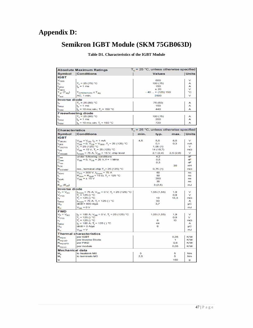
Appendix D:
Semikron IGBT Module (SKM 75GB063D) Table D1. Characteristics of the IGBT Module