Embed Size (px)
Citation preview

SHA3: Pipelining and interfaces with Exploration
CS250 Laboratory 2Written by Colin Scmidt
Modified by James MartinPortions based on previous work by Yunsup Lee
Updated by Christopher Yarp, Brian Zimmer, Rimas Avizienis, Ben Keller
Overview
For this lab you will be building on our previous implementation of Sha3 and tackling a few newimportant topics for accelerators. The first change you will make is to add a parameterized numberof pipeline stages to the previous datapath. You will also flesh out the interface the accelerator haswith other components in the system including the Rocket processor driving it and the memorysystem. The interface with the Rocket processor, the RoCC interface, will be given to you but youwill be responsible for updating the memory interface. The given memory interface represents alow performance implementation and can be improved drastically.
In addition, to these updates to the Chisel RTL you will also be using another CAD tool, DesignCompiler to synthesize your RTL into a gate-level netlist. In order to accomplish this synthesisacross the parameterized design you have created we will introduce another Berkeley tool, Jack-hammer, which will help us manage a design space exploration of our accelerator.
Deliverables
This lab is due Saturday, February 11th at 11:59 PM. The deliverables for this lab are:
• (a) your working Chisel RTL checked into your private git repository at Github
• (c) build results and reports generated by Chisel FIRRTL, VCS, and DC checked into yourgit repo (results and reports only! No binaries!)
• (d) written answers to the questions given at the end of this document checked into your gitrepository as writeup/report.pdf or writeup/report.txt
You are encouraged to discuss your design with others in the class, but you must write your owncode and turn in your own work.
VLSI Synthesis Introduction
Figure 1 illustrates the toolflow you will be using for the first lab. You will use Chisel to generateVerilog of your design. Using the tests you write you can verify the functionality of your RTLwithout the use of any CAD tools. Once you are satisfied with the quality of you design youcan then also use Chisel to generate a verilog implementation of it. You will use Synopsys VCS(vcs) to simulate and debug your verilog RTL design. Both tools are capable of producing a moredetailed debugging aid a vpd file. This extra detail comes at a slow down in simulation and isa less productive but sometimes necessary method. Another CAD tool Discovery VisualizationEnvironment (dve) can read and display a waveform view of the circuits operation. After you

CS250 Lab Assignment 2, Spring 2017 2
get your design right, you will use Synopsys Design Compiler (dc shell-xg-t) to synthesize thedesign. Synthesis is the process of transforming RTL into a gate-level netlist. Finally, VCS will beused to simulate the resulting netlist.
The diagram below illustrates how the tools work together.
Getting Started
The setup procedure mirrors that given in the first lab. Use the command
git pull template master
git submodule update --init --recursive
to pull in the latest version of the lab documents and well as all of the new dependencies. Therehas been a slight modification to the start-up scripts for this lab. Run
echo "source ~/.bash_profile" > ~/.bashrc
We also should link the temporary directory on the instructional filesystem. Run the followingcommands
ln -s /home/tmp/$USER tmp
Once you have pulled the latest template navigate to the lab2 directory. This directory containsthe following subdirectories: src contains your source code; build contains several nested subdirec-tories as well. The test build dir contains the generated files for simulating the Chisel code. Thebuild/vlsi contains a few directories to simulate your generated verilog(vlsi/generate-src),synthesize this verilog into a gate-level design(vlsi/dc-syn) and then simulate that gate leveldesign(vlsi/vcs-sim-gl-syn).
Baseline Design Overview
The baseline design for this lab has changed in several ways from the solution to Lab 1. Themost important change revolves around the new interface in the top level module Sha3Accel. Thismodule now implements the RoCC interface. This means that the module is notified that it hasa new hash to complete via two instructions set over the RoCC interface. The first instructionspecifies the memory addresses for the message to be read from and the hash to be written too.The design waits until it has received both of these instructions at which point it becomes busyand begins reading from memory and hashing the message.
The second important change is the use of memory to obtain the message to be hashed. Thebaseline design has a simple memory system that sends out one request and waits for its replybefore continuing.
Finally, a smaller change is that the accelerator now supports variable length messages and you areprovided with the control to manage this as well as the control to pad the messages appropriately.

CS250 Lab Assignment 2, Spring 2017 3
Execute SIM
VerilogSource(Behav)
BehavSim
VCS
VPD TestOutputs
DVE GUI
VerilogSource(RTL)
VCS Design Compiler
Design Vision GUI
ConstraintsFile
ConstraintsStd.Cell
Library
RTLSim
GateLevelNetlist
TimingArea
DelayFile
Execute SIM
VPD TestOutputs
DVE GUI
VCS
PostSynSim
Execute SIM
VPD TestOutputs
DVE GUI
Figure 1: CS250 Toolflow for Lab 2

CS250 Lab Assignment 2, Spring 2017 4
SHA3 Datapath: Pipelining
The first part of this lab involves pipelining your design in a parameterized fashion. The idea is todecrease the critical path in order to increase performance. As we have seen in class this increasein performance can also be traded for a decrease in energy if we are also able to scale the voltagedown.
The baseline design in this lab includes a new parameter S that corresponds to the number ofpipeline stages to complete one round of the Sha3 permutation. This baseline design also includesan implementation of this parameter for S=1 which was the design implemented for the previouslab. The baseline design also has a combined rhopi and so is designed to support S={1,2,4}. Ifyou are starting from the given design these are the only values your finished implementation needsupport. If you are using your previous design with separate rho and pi modules then you shouldchoose what set of values for S you should support but must support at least three distinct values.
The pipelining you will be implementing is slightly different than traditional pipelining becausewe are not adding additional state to keep track of multiple in-flight hashes at once. Rather youralteration will be more similar to a multi-cycle implementation, in which the larger operation hasbeen broken up into smaller segments that still end in the same piece of state at the end of each cycle.The reasons for this are two fold. First, not having multiple in flight hashes significantly reducesthe complexity of implementing this lab. And second, the additional state required to have multiplehashes in flight is significantly larger than the extra state in a processor for additional instructionsin flight. Both of these reasons don’t eliminate the potential usefullness of such a design and infact in a later lab we will implement just such a modification to gauge its effectiveness.
SHA3 Control: Memory Interface and RoCC Interfaces
The second part of the lab is to improve the design of the memory interface. The idea is that,in order to improve performance for the entire accelerator, all parts must be accelerated and thesimple memory interface given in the baseline can be a bottleneck and can be improved significantly.
Because this baseline design has added the ability to fetch the message from memory, this hasbecome another portion of the design in need of optimization. The memory system we use cansupport multiple in-flight requests and so there is the potential to improve the baseline design byallowing it to send multiple requests before waiting for their response. This will hopefully increasethe bandwidth obtained from the memory system.
Your task is to update the memory portion of the accelerator to send as many reads from onemessage chunk as it can before waiting for any responses. Keep in mind that we are not able toput back-pressure on the memory system so your accelerator must always be able to handle thememory responses when they arrive.
The baseline works only with the fast, instant, simulation memory. Your design should work willall three memories: instant, slow, and random.
Testing
The baseline design includes two tests. One mirrors the test given for Lab 1, which is intended tohelp validate that your design is functionally correct for a simple case. The second test is more of

CS250 Lab Assignment 2, Spring 2017 5
a benchmark in that it is designed to take longer and give you an idea the performance of yourdesign on a longer hash.
The tests are still implemented in scala and run from scala but some infrastructure has been addedto make it easier to develop tests for a RoCC accelerator that accesses memory. You can see thisextra infrastructure in test infrastructure.scala, and the given tests provide an example ofhow to use it. The infrastructure provides a model of memory as well as a simpler method ofmodeling the RoCC interface, other than poking all the individual bits. This encapsulation allowsfor a similar level of simplicity in our tests as we had in the first lab.
SHA3 Chisel Testing
In addition to the two methods of testing used in the previous lab, Verilator and RTL VCS, a newoption has been added this lab which is post synthesis level simulation. This last test is designedto be run after your design has been synthesised using Design Compiler (see below).
First, the Chisel compiler can test your code using the firrtl interpreter simulation of your design.The commands below will do this:
% cd $LABROOT
% make test-firrtl
To test using verilator, the following commands will do this:
% cd $LABROOT
% make test-verilator
Lastly to run using VCS, the following commands will do this:
% cd $LABROOT
% make test-vcs
In addition to simulation, the Chisel compiler can also generate Verilog code that can be used asinput to an ASIC flow.
% cd $LABROOT
% make verilog
The new tester for post synthesis gate level simulation is run from the Makefile with the followingcommands:
% cd $LABROOT
% make test-post-syn
Exploring Design Space and Generating Results
This section contains details on how to test different parameterization of your design, in an auto-mated fashion, as well as how to collect results from synthesis and simulations automatically.
The tool we will be using to explore the implications have our pipelining and memory interfacechanges is a new tool developed here at Berkeley called Jackhammer. Jackhammer uses the concept

CS250 Lab Assignment 2, Spring 2017 6
of ”knobs” and constraints to automatically generate a set of configurations. Previous versions ofJackhammer used Chisel Configs but this has recently been replaced with the Context DependentEnvironments (CDE) Package. The usage syntax remains similar to Chisel Configs but severalbackend features require alternate implementations. SHA3 and Jackhammer have been modified towork with CDE but some of the complexity surrounding CDE in the backend had to be includedin the source (especially in sha3.scala). This code is provided for you so you should not need toworry about it.
The first step to using Jackhammer is to parameterize your design using a Config object. You thendefine the set of knobs and the constraints on those knobs. This is already done for you in thegiven code, see the top of sha3.scala and topDefinitions at the bottom. You can see that we haveconstrained stages to be between 1 and 4, and divisible by 2 or equal to 1. Jackhammer will use aconstraint solver to determine what values it can fill in for the parameters.
Once we have defined our config, we can use Jackhammer to generate a few files to show itsunderstanding of the parameter space.
% cd $LABROOT/jackhammer
% make
This generates a directory inside of the main scala directory called config. This directory containsthree files, a .cst file listing the constraints that jackhammer has discovered from our definitions.The .knb file contains the names of the knobs in our design. Finally, the most important file forus is the .scala file which contains the names of each of the valid configurations. In our case, thisfile only contains three points, which is what we expected, each one setting stages to a differentdirectory.
With this file we can now setup what we want Jackhammer to do for us. If you open upjackhammer/DefaultSettings.scala you can see a bunch of boilerplate settings. The most im-portant things to note about this file are the scripts variables, the qors list and the designs list.Since we have configured Jackhammer to use this settings file it will use these variables to determinewhat it does. Explicitly Jackhammer will, for each design configuration in the designs list, executethe execute script and then the parse script for each of the listed qors.
Jackhammer is capable of distributing jobs across a server cluster, however, the servers we are usingare not currently configured to do this. We will be using Jackhammer to queue up and run jobs seri-ally on one machine. It will create a folder in the scratch directory /scratch/cs250-aa/hammer-data
which it will use to stage the different run and collect the results to. You should read over thescripts in the scripts directory to see what they are doing, in future labs you may be asked tomodify them.
Now that you understand what Jackhammer will do it is time to have it start. At this time, youmay only submit jobs from icluster1 to the cluster. You may read the results from any instserver. To run jackhammer you can execute the following commands:
% cd $LABROOT/jackhammer
% make parent
After running this command Jackhammer will submit the jobs to the servers, which you can monitoras follows.

CS250 Lab Assignment 2, Spring 2017 7
% qstat -u cs250-aa
Jackhammer will collect the results from stdout for each of the runs in /home/tmp/cs250-xx/hammer-data/sha3.0.0.0/results
The report files from each run can be found in /scratch/cs250-xx/hammer-data/sha3.0.0.0/DefaultConfig{0-2}/sources/build.There is one directory for each configuration. The reports are in the same location as in lab 1:build/firrtl-report build/vcs-report
You should copy the results files of your last run into the lab2/writeup directory and committhem for grading.
Synopsys Design Compiler: RTL to Gate-Level Netlist
You can choose to experiment with Design Compiler before, during, or after you implement theRTL changes. Either way the steps we take will be the same. The instructions below are designedto show you the steps the makefile must execute in order to synthesize your design, and are usefulto gain a better understand of how the tools work.
This section will also be updated later with more specific information with regards to Sha3 ratherthan GCD.
Design Compiler performs hardware synthesis. A synthesis tool takes an RTL hardware descriptionand a standard cell library as input and produces a gate-level netlist as an output. The resultinggate-level netlist is a completely structural description of the design, with only standard cells (andlater on, possibly SRAM macros) as leaves in the design hierarchy. To cut and past commands fromthis lab into your Design Compiler shell and make sure Design Compiler ignores the dc shell-topo>
string, we will use an alias to ”undefine” the dc shell-topo> string.
% cd $LABROOT/build/vlsi/dc-syn
% dc_shell-xg-t -64bit -topographical_mode
...
Initializing...
alias "dc_shell-topo>" ""
You will now execute some commands to setup your environment.
dc_shell-topo> set ucb_vlsi_home [getenv UCB_VLSI_HOME]
dc_shell-topo> set stdcells_home \
$ucb_vlsi_home/stdcells/synopsys-32nm/typical_rvt
dc_shell-topo> set_app_var search_path \
"$stdcells_home/db $ucb_vlsi_home/install/vclib ../generated-src"
dc_shell-topo> set_app_var target_library "cells.db"
dc_shell-topo> set_app_var synthetic_library "dw_foundation.sldb"
dc_shell-topo> set_app_var link_library "* $target_library $synthetic_library"
dc_shell-topo> set_app_var alib_library_analysis_path "alib"
dc_shell-topo> set_app_var mw_logic1_net "VDD"
dc_shell-topo> set_app_var mw_logic0_net "VSS"
dc_shell-topo> create_mw_lib -technology $stdcells_home/techfile/techfile.tf \
-mw_reference_library $stdcells_home/mw/cells.mw "Sha3Accel_LIB"
dc_shell-topo> open_mw_lib "Sha3Accel_LIB"

CS250 Lab Assignment 2, Spring 2017 8
dc_shell-topo> check_library
dc_shell-topo> set_tlu_plus_files \
-max_tluplus $stdcells_home/tluplus/max.tluplus \
-min_tluplus $stdcells_home/tluplus/min.tluplus \
-tech2itf_map $stdcells_home/techfile/tech2itf.map
dc_shell-topo> check_tlu_plus_files
dc_shell-topo> define_design_lib WORK -path "./work"
dc_shell-topo> set_svf "Sha3Accel.svf"
These commands point to your Verilog source directory, create a Synopsys work directory, andpoint to the standard libraries you will be using for the class. The set svf command is used to setup a guidance file which is used by Synopsys Formality. Now you can load your Verilog design into Design Compiler with the analyze, elaborate, link, and check design commands.
dc_shell-topo> analyze -format verilog \
"Sha3Accel.v"
dc_shell-topo> elaborate "Sha3Accel"
dc_shell-topo> link
dc_shell-topo> check_design
Before you can synthesize your design, you must specify some constraints; most importantly youmust tell the tool your target clock period. The following command tells the Design Compiler thatthe pin named clk is the clock and that your target clock period is 1 nanosecond.
dc_shell-topo> create_clock clk -name ideal_clock1 -period 1
Now you are ready to use the compile ultra command to actually synthesize your design into agate-level netlist. -no autoungroup is specified in order to preserve the hierarchy during syntehsis.
dc_shell-topo> compile_ultra -gate_clock -no_autoungroup
...
Beginning Delay Optimization
----------------------------
0:01:42 57293.5 0.00 0.0 0.0
0:01:42 57293.5 0.00 0.0 0.0
0:01:42 57293.5 0.00 0.0 0.0
0:01:42 57293.5 0.00 0.0 0.0
0:01:42 57293.5 0.00 0.0 0.0
0:01:42 57293.5 0.00 0.0 0.0
0:01:42 57293.5 0.00 0.0 0.0
0:01:42 57293.5 0.00 0.0 0.0
...
The compile ultra command will report how the design is being optimized. You should see DesignCompiler performing technology mapping, delay optimization, and area reduction. The fragmentfrom compile ultra above shows the worst negative slack which indicates how much room thereis between the critical path in your design and your specified clock constraint. Larger negativeslack values are worse since this means that your design is missing the desired clock frequency by agreat amount. Total negative slack is the sum of all negative slack summed over all the endpoints(register inputs or top level input/output ports) in the design.
CS250 Lab Assignment 2, Spring 2017 9
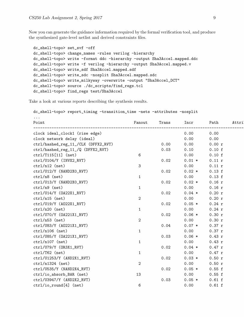
Now you can generate the guidance information required by the formal verification tool, and producethe synthesized gate-level netlist and derived constraints files.
dc_shell-topo> set_svf -off
dc_shell-topo> change_names -rules verilog -hierarchy
dc_shell-topo> write -format ddc -hierarchy -output Sha3Accel.mapped.ddc
dc_shell-topo> write -f verilog -hierarchy -output Sha3Accel.mapped.v
dc_shell-topo> write_sdf Sha3Accel.mapped.sdf
dc_shell-topo> write_sdc -nosplit Sha3Accel.mapped.sdc
dc_shell-topo> write_milkyway -overwrite -output "Sha3Accel_DCT"
dc_shell-topo> source ./dc_scripts/find_regs.tcl
dc_shell-topo> find_regs test/Sha3Accel
Take a look at various reports describing the synthesis results.
dc_shell-topo> report_timing -transition_time -nets -attributes -nosplit
...
Point Fanout Trans Incr Path Attributes
------------------------------------------------------------------------------------------------------
clock ideal_clock1 (rise edge) 0.00 0.00
clock network delay (ideal) 0.00 0.00
ctrl/hashed_reg_11_/CLK (DFFX2_RVT) 0.00 0.00 0.00 r
ctrl/hashed_reg_11_/Q (DFFX2_RVT) 0.03 0.10 0.10 f
ctrl/T115[11] (net) 6 0.00 0.10 f
ctrl/U104/Y (INVX2_RVT) 0.02 0.01 * 0.11 r
ctrl/n12 (net) 3 0.00 0.11 r
ctrl/U12/Y (NAND2X0_RVT) 0.02 0.02 * 0.13 f
ctrl/n8 (net) 1 0.00 0.13 f
ctrl/U13/Y (NAND2X0_RVT) 0.02 0.02 * 0.16 r
ctrl/n9 (net) 1 0.00 0.16 r
ctrl/U14/Y (OA22X1_RVT) 0.02 0.04 * 0.20 r
ctrl/n15 (net) 2 0.00 0.20 r
ctrl/U19/Y (AO22X1_RVT) 0.02 0.05 * 0.24 r
ctrl/n20 (net) 1 0.00 0.24 r
ctrl/U70/Y (OA221X1_RVT) 0.02 0.06 * 0.30 r
ctrl/n53 (net) 2 0.00 0.30 r
ctrl/U83/Y (AO221X1_RVT) 0.04 0.07 * 0.37 r
ctrl/n106 (net) 1 0.00 0.37 r
ctrl/U85/Y (OA221X1_RVT) 0.03 0.06 * 0.43 r
ctrl/n107 (net) 1 0.00 0.43 r
ctrl/U79/Y (OR3X1_RVT) 0.02 0.04 * 0.47 r
ctrl/T62 (net) 1 0.00 0.47 r
ctrl/U1253/Y (AND2X1_RVT) 0.02 0.03 * 0.50 r
ctrl/n1324 (net) 2 0.00 0.50 r
ctrl/U535/Y (NAND2X4_RVT) 0.02 0.05 * 0.55 f
ctrl/io_absorb_BAR (net) 13 0.00 0.55 f
ctrl/U3947/Y (AND2X2_RVT) 0.03 0.05 * 0.61 f
ctrl/io_round[4] (net) 6 0.00 0.61 f

CS250 Lab Assignment 2, Spring 2017 10
ctrl/io_round[4] (CtrlModule) 0.00 0.61 f
ctrl_io_round[4] (net) 0.00 0.61 f
dpath/io_round[4] (DpathModule) 0.00 0.61 f
dpath/iota/io_round[4] (IotaModule) 0.00 0.61 f
dpath/iota/io_round[4] (net) 0.00 0.61 f
dpath/iota/U5/Y (INVX4_RVT) 0.02 0.02 * 0.62 r
dpath/iota/n29 (net) 8 0.00 0.62 r
dpath/iota/U23/Y (AND2X1_RVT) 0.02 0.03 * 0.65 r
dpath/iota/n13 (net) 2 0.00 0.65 r
dpath/iota/U25/Y (AO22X1_RVT) 0.02 0.04 * 0.70 r
dpath/iota/n10 (net) 1 0.00 0.70 r
dpath/iota/U26/Y (AO22X1_RVT) 0.02 0.05 * 0.75 r
dpath/iota/n11 (net) 1 0.00 0.75 r
dpath/iota/U28/Y (NAND3X4_RVT) 0.03 0.07 * 0.82 f
dpath/iota/n12 (net) 1 0.00 0.82 f
dpath/iota/U29/SO (HADDX1_RVT) 0.02 0.07 * 0.88 r
dpath/iota/io_state_o_0[15] (net) 1 0.00 0.88 r
dpath/iota/io_state_o_0[15] (IotaModule) 0.00 0.88 r
dpath/iota_io_state_o_0[15] (net) 0.00 0.88 r
dpath/U2349/Y (AO22X1_RVT) 0.02 0.05 * 0.93 r
dpath/N41 (net) 1 0.00 0.93 r
dpath/state_0_reg_15_/D (DFFX2_RVT) 0.02 0.00 * 0.93 r
data arrival time 0.93
clock ideal_clock1 (rise edge) 1.00 1.00
clock network delay (ideal) 0.00 1.00
dpath/state_0_reg_15_/CLK (DFFX2_RVT) 0.00 1.00 r
library setup time -0.03 0.97
data required time 0.97
------------------------------------------------------------------------------------------------------
data required time 0.97
data arrival time -0.93
------------------------------------------------------------------------------------------------------
slack (MET) 0.04
...
This report shows the critical path of the design. The critical path has the longest propagationdelay between any two registers in the design and therefore sets an upper bound on the design’soperating frequency. In this report, we see that the critical path begins at the output of bit 2of the operand A register in the datapath, goes several subtractors in the datapath, and ends atoutput register 15. The critical path takes a total of 0.91ns which is less than the 1ns clock periodconstraint. This is reflected by the final line declaring that the positive slack has met timing.
dc_shell-topo> report_area -nosplit -hierarchy
...
Global cell area Local cell area

CS250 Lab Assignment 2, Spring 2017 11
------------------- ------------------------------
Hierarchical cell Absolute Percent Combi- Noncombi- Black
Total Total national national boxes Design
-------------------------------- ---------- ------- ---------- ---------- ------ -------------------------------
Sha3Accel 59792.2057 100.0 507.7797 0.0000 0.0000 Sha3Accel
ctrl 19785.8732 33.1 9841.7265 9780.4779 0.0000 CtrlModule
...
dpath 39498.5528 66.1 8319.4041 10953.0984 0.0000 DpathModule
...
-------------------------------- ---------- ------- ---------- ---------- ------ --------------------------------
Total 38883.2700 20908.9357 0.0000
...
This report tells you about the post synthesis area results. The units are um2. You can see thatthe datapath accounts for 91.8% of the total chip area.
dc_shell-topo> report_power -nosplit -hier
...
--------------------------------------------------------------------------------
Switch Int Leak Total
Hierarchy Power Power Power Power %
--------------------------------------------------------------------------------
Sha3Accel 2.48e+03 1.09e+04 8.11e+09 2.14e+04 100.0
dpath (DpathModule) 1.36e+03 5.25e+03 5.47e+09 1.21e+04 56.3
iota (IotaModule) 1.246 1.510 1.11e+07 13.851 0.1
ChiModule (ChiModule) 0.000 0.000 1.05e+09 1.05e+03 4.9
RhoPiModule (RhoPiModule) 0.000 0.000 0.000 0.000 0.0
ThetaModule (ThetaModule) 0.000 0.000 1.52e+09 1.52e+03 7.1
ctrl (CtrlModule) 1.13e+03 5.60e+03 2.60e+09 9.33e+03 43.5
...
This report contains post synthesis power estimates. The dynamic power units are uW while theleakage power units are pW .
dc_shell-topo> report_reference -nosplit -hierarchy
...
****************************************
Design: DpathModule
****************************************
Reference Library Unit Area Count Total Area Attributes
-----------------------------------------------------------------------------
AND2X1_RVT saed32rvt_tt1p05v25c 2.033152 512 1040.973877
AND3X4_RVT saed32rvt_tt1p05v25c 3.049728 1 3.049728
AO22X1_RVT saed32rvt_tt1p05v25c 2.541440 1088 2765.086731
ChiModule 9895.605033 1 9895.605033 h
DFFX1_RVT saed32rvt_tt1p05v25c 6.607744 851 5623.190329 n
DFFX2_RVT saed32rvt_tt1p05v25c 7.116032 749 5329.908061 n
HADDX1_RVT saed32rvt_tt1p05v25c 3.303872 1082 3574.789621 r
HADDX2_RVT saed32rvt_tt1p05v25c 3.812160 6 22.872960 r
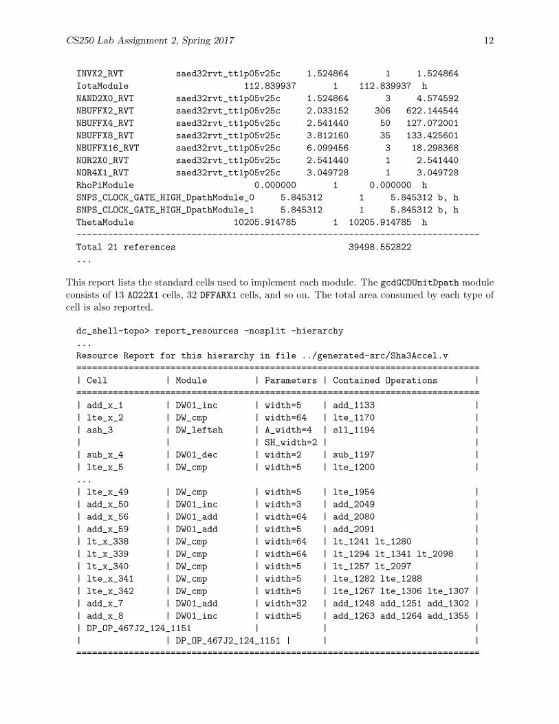
CS250 Lab Assignment 2, Spring 2017 12
INVX2_RVT saed32rvt_tt1p05v25c 1.524864 1 1.524864
IotaModule 112.839937 1 112.839937 h
NAND2X0_RVT saed32rvt_tt1p05v25c 1.524864 3 4.574592
NBUFFX2_RVT saed32rvt_tt1p05v25c 2.033152 306 622.144544
NBUFFX4_RVT saed32rvt_tt1p05v25c 2.541440 50 127.072001
NBUFFX8_RVT saed32rvt_tt1p05v25c 3.812160 35 133.425601
NBUFFX16_RVT saed32rvt_tt1p05v25c 6.099456 3 18.298368
NOR2X0_RVT saed32rvt_tt1p05v25c 2.541440 1 2.541440
NOR4X1_RVT saed32rvt_tt1p05v25c 3.049728 1 3.049728
RhoPiModule 0.000000 1 0.000000 h
SNPS_CLOCK_GATE_HIGH_DpathModule_0 5.845312 1 5.845312 b, h
SNPS_CLOCK_GATE_HIGH_DpathModule_1 5.845312 1 5.845312 b, h
ThetaModule 10205.914785 1 10205.914785 h
-----------------------------------------------------------------------------
Total 21 references 39498.552822
...
This report lists the standard cells used to implement each module. The gcdGCDUnitDpath moduleconsists of 13 AO22X1 cells, 32 DFFARX1 cells, and so on. The total area consumed by each type ofcell is also reported.
dc_shell-topo> report_resources -nosplit -hierarchy
...
Resource Report for this hierarchy in file ../generated-src/Sha3Accel.v
=============================================================================
| Cell | Module | Parameters | Contained Operations |
=============================================================================
| add_x_1 | DW01_inc | width=5 | add_1133 |
| lte_x_2 | DW_cmp | width=64 | lte_1170 |
| ash_3 | DW_leftsh | A_width=4 | sll_1194 |
| | | SH_width=2 | |
| sub_x_4 | DW01_dec | width=2 | sub_1197 |
| lte_x_5 | DW_cmp | width=5 | lte_1200 |
...
| lte_x_49 | DW_cmp | width=5 | lte_1954 |
| add_x_50 | DW01_inc | width=3 | add_2049 |
| add_x_56 | DW01_add | width=64 | add_2080 |
| add_x_59 | DW01_add | width=5 | add_2091 |
| lt_x_338 | DW_cmp | width=64 | lt_1241 lt_1280 |
| lt_x_339 | DW_cmp | width=64 | lt_1294 lt_1341 lt_2098 |
| lt_x_340 | DW_cmp | width=5 | lt_1257 lt_2097 |
| lte_x_341 | DW_cmp | width=5 | lte_1282 lte_1288 |
| lte_x_342 | DW_cmp | width=5 | lte_1267 lte_1306 lte_1307 |
| add_x_7 | DW01_add | width=32 | add_1248 add_1251 add_1302 |
| add_x_8 | DW01_inc | width=5 | add_1263 add_1264 add_1355 |
| DP_OP_467J2_124_1151 | | |
| | DP_OP_467J2_124_1151 | | |
=============================================================================

CS250 Lab Assignment 2, Spring 2017 13
...
Implementation Report
===============================================================================
| | | Current | Set |
| Cell | Module | Implementation | Implementation |
===============================================================================
| add_x_1 | DW01_inc | apparch (area) | |
| lte_x_2 | DW_cmp | apparch (area) | |
| ash_3 | DW_leftsh | astr (area) | |
| sub_x_4 | DW01_dec | apparch (area) | |
| lte_x_5 | DW_cmp | apparch (area) | |
| add_x_6 | DW01_add | pparch (area,speed) |
| add_x_9 | DW01_inc | apparch (area) | |
| lt_x_10 | DW_cmp | apparch (area) | |
| lt_x_11 | DW_cmp | pparch (speed) | |
...
| lt_x_340 | DW_cmp | apparch (area) | |
| lte_x_341 | DW_cmp | apparch (area) | |
| lte_x_342 | DW_cmp | apparch (area) | |
| add_x_7 | DW01_add | pparch (speed) | |
| add_x_8 | DW01_inc | apparch (area) | |
| DP_OP_467J2_124_1151 | | |
| | DP_OP_467J2_124_1151 | str (area) | |
===============================================================================
...
Synopsys provides a library of commonly used arithmetic components as highly optimized buildingblocks. This library is called Design Ware and Design Compiler will automatically use DesignWare components when it can. This report can help you determine when Design Compiler is usingDesign Ware components. The DW01 sub in the module name indicates that this is a Design Waresubtractor. This report also gives you what type of architecture it used.
You can use makefiles and scripts to help automate the process of synthesizing your design. Typeexit to leave the DC shell. Then type:
% cd $LABROOT/build/dc-syn
% make
Go ahead and take a look what the automated build system produced.
% cd $LABROOT/build/dc-syn
% ls -l
total 20
drwx------ 3 cs250 cs250 4096 Sep 12 06:13 alib
drwxr-xr-x 7 cs250 cs250 4096 Sep 16 14:18 build-dc-01.250ns-2014-09-16_14-13
lrwxrwxrwx 1 cs250 cs250 34 Sep 16 14:13 current-dc -> build-dc-01.250ns-2014-09-16_14-13

CS250 Lab Assignment 2, Spring 2017 14
drwx------ 2 cs250 cs250 4096 Sep 12 06:13 dc_scripts
-rw------- 1 cs250 cs250 1062 Sep 12 06:13 Makefile
-rw------- 1 cs250 cs250 3963 Sep 12 06:13 Makefrag
lrwxrwxrwx 1 cs250 cs250 8 Sep 12 06:13 setup -> ../setup
% cd current-dc
% ls -l
total 856
-rw-r--r-- 1 cs250 cs250 37 Sep 16 14:18 access.tab
-rw-r--r-- 1 cs250 cs250 370697 Sep 16 14:18 command.log
-rw------- 1 cs250 cs250 5139 Sep 16 14:13 common_setup.tcl
-rw------- 1 cs250 cs250 3632 Sep 16 14:13 constraints.tcl
-rw-r--r-- 1 cs250 cs250 29 Sep 16 14:18 dc
-rw------- 1 cs250 cs250 4625 Sep 16 14:13 dc_setup_filenames.tcl
-rw------- 1 cs250 cs250 4914 Sep 16 14:13 dc_setup.tcl
-rw------- 1 cs250 cs250 4612 Sep 16 14:13 dc.tcl
-rw------- 1 cs250 cs250 2720 Sep 16 14:13 find_regs.tcl
-rw-r--r-- 1 cs250 cs250 420655 Sep 16 14:18 force_regs.ucli
drwxr-xr-x 2 cs250 cs250 4096 Sep 16 14:13 log
-rw------- 1 cs250 cs250 3686 Sep 16 14:13 Makefrag
-rw-r--r-- 1 cs250 cs250 1387 Sep 16 14:13 make_generated_vars.tcl
drwxr-xr-x 2 cs250 cs250 4096 Sep 16 14:18 reports
drwxr-xr-x 2 cs250 cs250 4096 Sep 16 14:18 results
drwxr-xr-x 2 cs250 cs250 4096 Sep 16 14:13 Sha3Accel_LIB
-rw-r--r-- 1 cs250 cs250 29 Sep 16 14:13 timestamp
drwxr-xr-x 2 cs250 cs250 4096 Sep 16 14:13 WORK
Notice that the Makefile does not overwrite build directories. It creates a new build directoryevery time you run make. This makes it easy to change your synthesis scripts or source Verilog,resynthesize your design, and compare your results to those from an earlier design. You can usesymlinks to keep track of various build directories. Inside the current-dc directory, you can seeall the tcl scripts as well as the directories named results and reports. results contains yoursynthesized gate-level netlist, and reports contains various post synthesis reports.
Synopsys provides a GUI front-end for Design Compiler called Design Vision which you will useto analyze the synthesis results. You should avoid using the GUI to actually perform synthesissince scripting the process is more efficient. Start Design Vision, and open the ddc file to loadyour synthesized design. (.ddc is a proprietary binary format used by Synopsys to encapsulate allpost-synthesis data.)
% cd $LABROOT/build/dc-syn/current-dc
% design_vision-xg -64bit
...
Initializing...
design_vision> alias "design_vision>" ""
design_vision> source dc_setup.tcl
design_vision> read_file -format ddc "results/Sha3Accel.mapped.ddc"
You can browse your design with the hierarchical view (see Figure 2). If you right click on a moduleand select the Schematic View option, the tool will display a schematic view of the standard cells

CS250 Lab Assignment 2, Spring 2017 15
used to implement that module.
Figure 2: Design Vision Hierarchical View
CS250 Lab Assignment 2, Spring 2017 16
Questions
Your writeup should not exceed one page in length. Make your writing as crisp as you can! Thesequestions are intended to be thought provoking rather than work intensive.
Q1. Chisel and Jackhammer
• Do you feel the combination of Chisel and Jackhammer helped you for this lab?
• Are there features you would like to see in Chisel and/or Jackhammer that could improveyour experience?
• Other than the obvious bugs noted on piazza are there any issues you encountered.
Q2. Pipelined exploration
• Which of the design you synthesized has the best performance in terms of Gigabits hashedper second?
• Which of the design you synthesized has the best performance/energy in terms of Gigabitshashed per second per joule?
• What do you believe to be the bottlenecks for each of your design points?
• What would you recommend to alleviate these bottlenecks?
Read me before you commit!
This section will be updated later with submission instructions
• Commiting is not enough for us to grade this lab. You will also need to push your changesto github with the following command: git push origin master
• Please note in your writeup if you discussed or received help with the lab from others in thecourse. This will not affect your grade, but is useful in the interest of full disclosure.
• Please note in your writeup (roughly) how many hours you spent on this lab in total.
• To summarize, your Git tree for lab2 should look like the following (use the Github webbrowser to check that everything is there):
/cs250-ab
/lab2
/src: COMMIT CHISEL CODE
/jackhammer: original files only
/chisel: original files only
/build:
/vlsi: original files only
/generated-src: original files only
/writeup: COMMIT REPORT
/results: COMMIT Jackhammer results for S={1,2,4} and instant, random and slow memory unit

CS250 Lab Assignment 2, Spring 2017 17
Acknowledgements
Many people have contributed to versions of this lab over the years. The lab was originally de-veloped for CS250 VLSI Systems Design course at University of California at Berkeley by YunsupLee. Original contributors include: Krste Asanovic, Christopher Batten, John Lazzaro, and JohnWawrzynek. Versions of this lab have been used in the following courses:
• CS250 VLSI Systems Design (2009-2013) - University of California at Berkeley
• CSE291 Manycore System Design (2009) - University of California at San Diego