Embed Size (px)
Citation preview
SEU sensitivity and modeling using picosecond pulsed
laser stimulation of a D Flip-Flop in 40 nm CMOS
technology
Clement Champeix, Nicolas Borrel, Jean-Max Dutertre, Bruno Robisson,
Mathieu Lisart, Alexandre Sarafianos
To cite this version:
Clement Champeix, Nicolas Borrel, Jean-Max Dutertre, Bruno Robisson, Mathieu Lisart, etal.. SEU sensitivity and modeling using picosecond pulsed laser stimulation of a D Flip-Flopin 40 nm CMOS technology. Defect and Fault Tolerance in VLSI and Nanotechnology Sys-tems (DFTS), 2015 IEEE International Symposium on, Oct 2015, Amherst, United States.<10.1109/DFT.2015.7315158>. <emse-01227355v2>
HAL Id: emse-01227355
https://hal-emse.ccsd.cnrs.fr/emse-01227355v2
Submitted on 17 Nov 2015

HAL is a multi-disciplinary open accessarchive for the deposit and dissemination of sci-entific research documents, whether they are pub-lished or not. The documents may come fromteaching and research institutions in France orabroad, or from public or private research centers.
L’archive ouverte pluridisciplinaire HAL, estdestinee au depot et a la diffusion de documentsscientifiques de niveau recherche, publies ou non,emanant des etablissements d’enseignement et derecherche francais ou etrangers, des laboratoirespublics ou prives.
SEU sensitivity and modeling using picosecondpulsed laser stimulation of a D Flip-Flop in 40 nm
CMOS technology
Clement Champeix∗†, Nicolas Borrel∗‡, Jean-Max Dutertre†, Bruno Robisson§, Mathieu Lisart∗and Alexandre Sarafianos∗
∗STMicroelectronics, Secure Microcontrollers Division (SMD), 190 avenue Celestin Coq, 13106 Rousset, France†Ecole Nationale Superieure des Mines de Saint-Etienne, Laboratoire Secure Architectures and Systems (LSAS)
Centre de Microelectronique de Provence, 880 route de Mimet, 13541 Gardanne, France‡Aix Marseille Universite, CNRS, Universite de Toulon, IM2NP UMR 7334, 13397, Marseille, France
§CEA Cadarache, 13108, Saint-Paul-lez-Durance, France
Abstract—This paper presents the design of a CMOS 40 nmD Flip-Flop cell and reports the laser fault sensitivity mappingboth with experiments and simulation results. Theses studies aredriven by the need to propose a simulation methodology basedon laser/silicon interactions with a complex integrated circuit.In the security field, it is therefore mandatory to understand thebehavior of sensitive devices like D Flip-Flops to laser stimulation.In previous works, Roscian et al., Sarafianos et al., Lacruche etal. or Courbon et al. studied the relations between the layout ofcells, its different laser-sensitive areas and their associated faultmodel using laser pulse duration in the nanosecond range. In thispaper, we report similar experiments carried out using a shorterlaser pulse duration (30 ps instead of 50 ns). We also propose anupgrade of the simulation model they used to take into accountlaser pulse durations in the picosecond range on a logic gatecomposed of a large number of transistors for a recent CMOStechnology (40 nm).
Keywords—D Flip-Flop cell, Hardware Security, PhotoelectricLaser Stimulation, Single Event Effects, Laser Fault Injection,Electrical Modeling
I. INTRODUCTION
When exposed to a harsh environment in space, highatmosphere or even on earth, integrated circuits (ICs) mayundergo soft errors. The related phenomena have been knownand studied for more than forty years [1–3]. Among the variousexisting phenomena, single event effects (SEEs) due to ionizingparticles may result in a faulty behavior of the hit circuit. Forthis reason and in order to cope with the effects of such events,a lot of research work has been devoted to the understandingand mitigation of SEEs. In this context, the use of pulsed-lasers was introduced to emulate SEEs [4], [5]. However,another usage of the pulsed-laser is to intentionally inducefaults (as a result of SEEs) in security-dedicated ICs in orderto retrieve or modify the secret data they may contain [6], [7].Fortunately, other techniques introduced by researchers fromthe radiation community to mitigate SEEs may be adapted tocope with the issue of laser fault-injection. Electrical modelshave been created in order to propose a fast and simulatedanalysis (SPICE) of a circuit under laser stimulation. Theseelectrical models make it possible to simulate the responseof integrated circuits to laser pulses in very small amount of
calculation times by comparison with physical experiments onlaser equipment or TCAD simulation. The novelty of this paperis that our model takes into account very short laser pulsedurations with a thin spatial accuracy to identify sensitive areasfor a recent CMOS technology (40nm instead of 0.25µm or90nm).
This paper is organized as follows: Section II describes theprinciples of laser fault injection. Section III introduces theD Flip-Flop architecture used in our experiments. Hypothesisare made and validated both with experiments (Section IV)and modeling (Section V). Weaknesses and strengths, revealedduring the testing, are discussed afterward. A laser pulseduration in the picosecond range for emulating SEEs [5] wasused. Then, Section VI draws a conclusion.
II. STATE OF THE ART
ICs are known to be impacted by SEEs caused by ionizingparticles in radioactive environments. The related electricalphenomenon and the laser impacts on gates, as latches, SRAM(Static Random Access Memory) or D Flip-Flop, are reviewedin the following subsections.
A. Single Event Effects in Integrated Circuits
When an ionic particle passes through silicon, it generateselectron-hole pairs along its path. These electrical chargesgenerally recombine without any significant effect on IC com-putations. However the electric field found in reverse-biasedPN junctions may separate the electron-hole pairs, inducing aparasitic transient current. This transient current may in turndisturb the voltage across the IC’s internal nodes, leading tocomputational errors. A pulsed laser may be used to mimic (oremulate) this phenomenon provided that its photons energyis bigger than the silicon bandgap (electron-hole pairs arethen induced by photoelectric effect [4], [5]). At first, pulsedlasers were used to emulate SEE generation in ICs for radiationhardness evaluation. Since then, they have also been used toinduce faults into secure circuits for the purpose of retrievingconfidential data stored into these devices [6], [7]. In thefollowing, laser-induced SEEs are described. A laser-inducedtransient current is then called a ‘photocurrent’ [8–16].
178978-1-4799-8606-4/15/$31.00 c⃝2015 IEEE
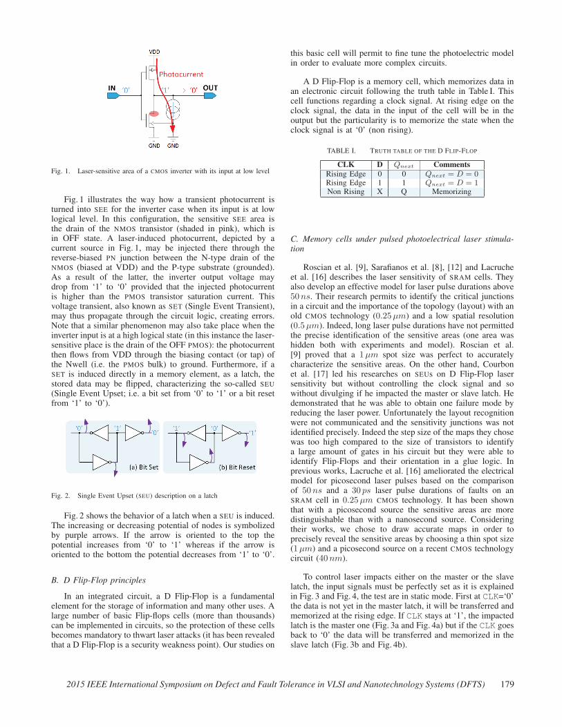
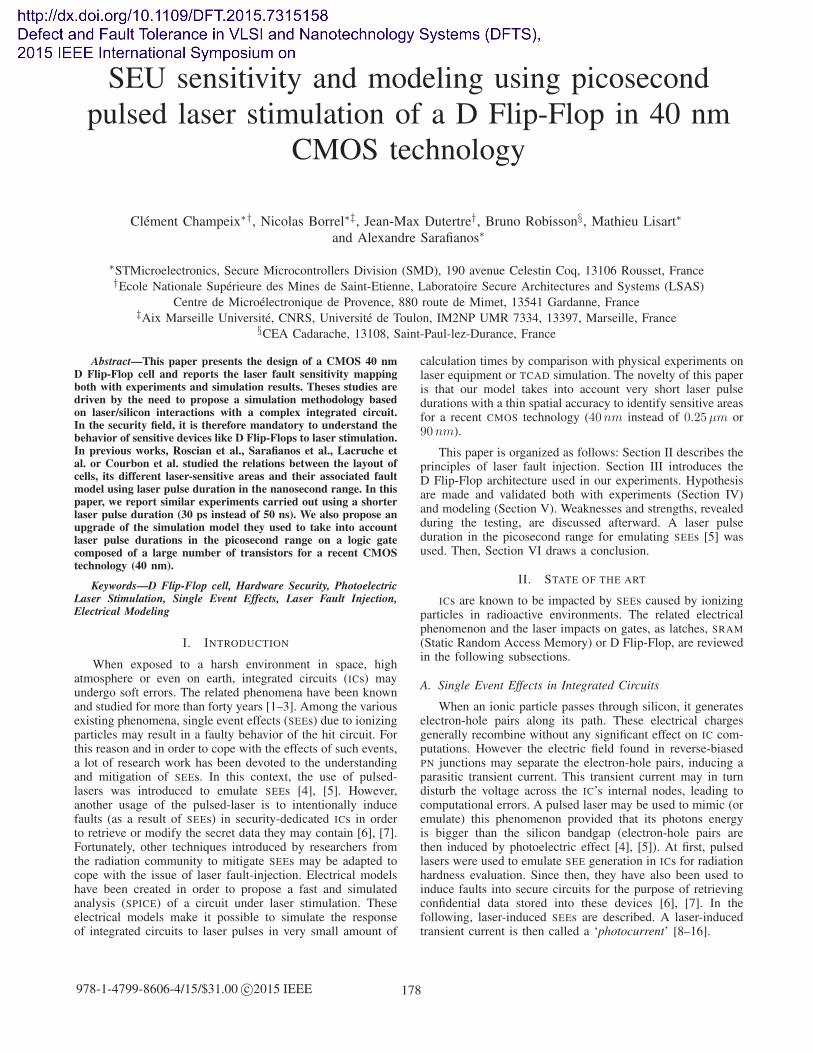
Fig. 1. Laser-sensitive area of a CMOS inverter with its input at low level
Fig. 1 illustrates the way how a transient photocurrent isturned into SEE for the inverter case when its input is at lowlogical level. In this configuration, the sensitive SEE area isthe drain of the NMOS transistor (shaded in pink), which isin OFF state. A laser-induced photocurrent, depicted by acurrent source in Fig. 1, may be injected there through thereverse-biased PN junction between the N-type drain of theNMOS (biased at VDD) and the P-type substrate (grounded).As a result of the latter, the inverter output voltage maydrop from ‘1’ to ‘0’ provided that the injected photocurrentis higher than the PMOS transistor saturation current. Thisvoltage transient, also known as SET (Single Event Transient),may thus propagate through the circuit logic, creating errors.Note that a similar phenomenon may also take place when theinverter input is at a high logical state (in this instance the laser-sensitive place is the drain of the OFF PMOS): the photocurrentthen flows from VDD through the biasing contact (or tap) ofthe Nwell (i.e. the PMOS bulk) to ground. Furthermore, if aSET is induced directly in a memory element, as a latch, thestored data may be flipped, characterizing the so-called SEU(Single Event Upset; i.e. a bit set from ‘0’ to ‘1’ or a bit resetfrom ‘1’ to ‘0’).
Fig. 2. Single Event Upset (SEU) description on a latch
Fig. 2 shows the behavior of a latch when a SEU is induced.The increasing or decreasing potential of nodes is symbolizedby purple arrows. If the arrow is oriented to the top thepotential increases from ‘0’ to ‘1’ whereas if the arrow isoriented to the bottom the potential decreases from ‘1’ to ‘0’.
B. D Flip-Flop principles
In an integrated circuit, a D Flip-Flop is a fundamentalelement for the storage of information and many other uses. Alarge number of basic Flip-flops cells (more than thousands)can be implemented in circuits, so the protection of these cellsbecomes mandatory to thwart laser attacks (it has been revealedthat a D Flip-Flop is a security weakness point). Our studies on
this basic cell will permit to fine tune the photoelectric modelin order to evaluate more complex circuits.
A D Flip-Flop is a memory cell, which memorizes data inan electronic circuit following the truth table in Table I. Thiscell functions regarding a clock signal. At rising edge on theclock signal, the data in the input of the cell will be in theoutput but the particularity is to memorize the state when theclock signal is at ‘0’ (non rising).
TABLE I. TRUTH TABLE OF THE D FLIP-FLOP
CLK D Qnext CommentsRising Edge 0 0 Qnext = D = 0Rising Edge 1 1 Qnext = D = 1Non Rising X Q Memorizing
C. Memory cells under pulsed photoelectrical laser stimula-tion
Roscian et al. [9], Sarafianos et al. [8], [12] and Lacrucheet al. [16] describes the laser sensitivity of SRAM cells. Theyalso develop an effective model for laser pulse durations above50ns. Their research permits to identify the critical junctionsin a circuit and the importance of the topology (layout) with anold CMOS technology (0.25µm) and a low spatial resolution(0.5µm). Indeed, long laser pulse durations have not permittedthe precise identification of the sensitive areas (one area washidden both with experiments and model). Roscian et al.[9] proved that a 1µm spot size was perfect to accuratelycharacterize the sensitive areas. On the other hand, Courbonet al. [17] led his researches on SEUs on D Flip-Flop lasersensitivity but without controlling the clock signal and sowithout divulging if he impacted the master or slave latch. Hedemonstrated that he was able to obtain one failure mode byreducing the laser power. Unfortunately the layout recognitionwere not communicated and the sensitivity junctions was notidentified precisely. Indeed the step size of the maps they chosewas too high compared to the size of transistors to identifya large amount of gates in his circuit but they were able toidentify Flip-Flops and their orientation in a glue logic. Inprevious works, Lacruche et al. [16] ameliorated the electricalmodel for picosecond laser pulses based on the comparisonof 50ns and a 30 ps laser pulse durations of faults on anSRAM cell in 0.25µm CMOS technology. It has been shownthat with a picosecond source the sensitive areas are moredistinguishable than with a nanosecond source. Consideringtheir works, we chose to draw accurate maps in order toprecisely reveal the sensitive areas by choosing a thin spot size(1µm) and a picosecond source on a recent CMOS technologycircuit (40nm).
To control laser impacts either on the master or the slavelatch, the input signals must be perfectly set as it is explainedin Fig. 3 and Fig. 4, the test are in static mode. First at CLK=‘0’the data is not yet in the master latch, it will be transferred andmemorized at the rising edge. If CLK stays at ‘1’, the impactedlatch is the master one (Fig. 3a and Fig. 4a) but if the CLK goesback to ‘0’ the data will be transferred and memorized in theslave latch (Fig. 3b and Fig. 4b).
2015 IEEE International Symposium on Defect and Fault Tolerance in VLSI and Nanotechnology Systems (DFTS) 179
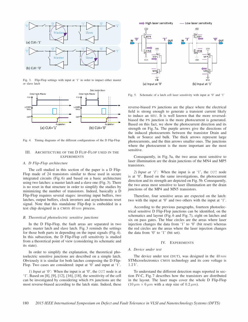
Fig. 3. Flip-Flop settings with input at ‘1’ in order to impact either masteror slave latch
Fig. 4. Timing diagrams of the different configurations of the D Flip-Flop
III. ARCHITECTURE OF THE D FLIP-FLOP USED IN THEEXPERIMENTS
A. D Flip-Flop architecture
The cell studied in this section of the paper is a D Flip-Flop made of 24 transistors similar to those used in secureintegrated circuits (Fig. 6) and based on a basic architectureusing two latches: a master latch and a slave one (Fig. 3). Thereis no reset in that structure in order to simplify the studies byminimizing the number of transistors. Indeed, basically a DFlip-Flop requires several stages: inverting input buffers, twolatches, output buffers, clock inverters and asynchronous resetsignal. Note that this standalone Flip-flop is embedded in atest chip designed in a CMOS 40nm process.
B. Theoretical photoelectric sensitive junctions
In the D Flip-Flop, the fault areas are separated in twoparts: master latch and slave latch. Fig. 3 reminds the settingsfor those both parts in depending on the input signals (Fig. 4).In this subsection, the D Flip-Flop cell sensitivity is studiedfrom a theoretical point of view (considering its schematic andits state).
In order to simplify the explanation, the theoretical pho-toelectric sensitive junctions are described on a simple latch.Obviously it is similar for both latches composing the D Flip-Flop. Two cases are considered: input at ‘0’ and input at ‘1’.
1) Input at ‘0’: When the input is at ‘0’, the OUT node is at‘1’. Based on [8], [9], [12], [16], [18], the sensitivity of the cellcan be investigated by considering which PN junctions are themost reverse-biased according to the latch state. Indeed, these
Fig. 5. Schematic of a latch cell laser sensitivity with input at ‘0’ and ‘1’
reverse-biased PN junctions are the place where the electricalfield is strong enough to generate a transient current likelyto induce an SEU. It is well known that the more reversed-biased the PN junction is the more photocurrent is generated.Based on this fact, we show the photocurrent direction and itsstrength on Fig. 5a. The purple arrows give the directions ofthe induced photocurrents between the transistor Drain andbulk or Source and bulk. The thick arrows represent largephotocurrents, and the thin arrows smaller ones. The junctionswhere the photocurrent is the more important are the mostsensitive.
Consequently, in Fig. 5a, the two areas most sensitive tolaser illumination are the drain junctions of the MN4 and MP5transistors.
2) Input at ‘1’: When the input is at ‘1’, the OUT nodeis at ‘0’. Based on the same investigations, the photocurrentdirection and its strength are depicted on Fig. 5b. Consequently,the two areas most sensitive to laser illumination are the drainjunctions of the MP4 and MN5 transistors.
Therefore, four sensitive areas are expected on the latch:two with the input at ‘0’ and two others with the input at ‘1’.
According to the previous paragraphs, fourteen photoelec-trical sensitive D Flip-Flop junctions can be identified, on theschematics and layout (Fig. 6 and Fig. 7), eight on latches andsix on pass gates. The blue circles are the areas where laserinjection changes the data from ‘1’ to ‘0’ (bit reset) whereasthe red circles are the areas where the laser injection changesthe data from ‘0’ to ‘1’ (bit set).
IV. EXPERIMENTS
A. Device under test
The device under test (DUT), was designed in the 40nmSTMicroelectronics CMOS technology and its core voltage is1.2V .
To understand the different detection maps reported in sec-tion IV-C, Fig. 7 describes how the transistors are distributedin the layout. The laser maps cover the whole D Flip-Flop(10µm× 6µm with a step size of 0.2µm).
180 2015 IEEE International Symposium on Defect and Fault Tolerance in VLSI and Nanotechnology Systems (DFTS)
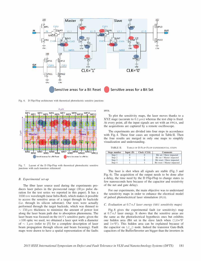
Fig. 6. D Flip-Flop architecture with theoretical photoelectric sensitive junctions
Fig. 7. Layout of the D Flip-Flop with theoretical photoelectric sensitivejunctions with each transitors referenced
B. Experimental set-up
The fiber laser source used during the experiments pro-duces laser pulses in the picosecond range (30 ps pulse du-ration for the test series we reported in this paper). It has a1030nm wavelength (near Infra-Red), which makes it possibleto access the sensitive areas of a target through its backside(i.e. through its silicon substrate). Our tests were actuallyperformed through the target backside, which was thinned to∼ 150µm thickness to minimize the amount of power lostalong the laser beam path due to absorption phenomena. Thelaser beam was focused on the DUT’s sensitive parts: given the×100 optic we used, we obtained a laser spot with a diameterof ∼ 1µm (refer to [5] for a complete description of laserbeam propagation through silicon and beam focusing). Faultmaps were drawn to have a spatial representation of the faults
area.
To plot the sensitivity maps, the laser moves thanks to aXYZ stage (accurate to 0.1µm) whereas the test chip is fixed.At every point, all the input signals are set with an FPGA, andthe acquisitions are captured by a remote oscilloscope.
The experiments are divided into four steps in accordancewith Fig. 4. These four cases are reported in Table II. Thenthe four results are merged in only one maps to simplifyvisualization and understanding.
TABLE II. TABLE OF D FLIP-FLOP EXPERIMENTAL STEPS
Steps number Input (D) Clock (CLK) CommentsStep 1 0 0 Bit set / Slave impactedStep 2 0 1 Bit set / Master impactedStep 3 1 0 Bit reset / Slave impactedStep 4 1 1 Bit reset / Master impacted
The laser is shot when all signals are stable (Fig. 3 andFig. 4). The acquisition of the output needs to be done aftera delay, the time need by the D Flip-Flop to change states (afew nanoseconds here because of the capacitor and resistivityof the net and gate delay).
For our experiments, the main objective was to understandthe sensitivity maps in order to enhance the electrical modelof pulsed photoelectrical laser stimulation (PLS).
C. Evaluation at 0.7nJ laser energy (SEU sensitivity maps)
Fig. 8 gives the experimental fault (or sensitivity) mapat 0.7nJ laser energy. It shows that the sensitive areas arethe same as the photoelectrical hypothesis ones but exhibitsone hidden area (Bit set in the slave latch when CLK=‘0’and D=‘0’). This hidden area can be explained because ofthe capacitor on L2_O node. Indeed the transistor Gate-Bulkcapacitors of the Buffer/Inverter are bigger than the inverters in
2015 IEEE International Symposium on Defect and Fault Tolerance in VLSI and Nanotechnology Systems (DFTS) 181
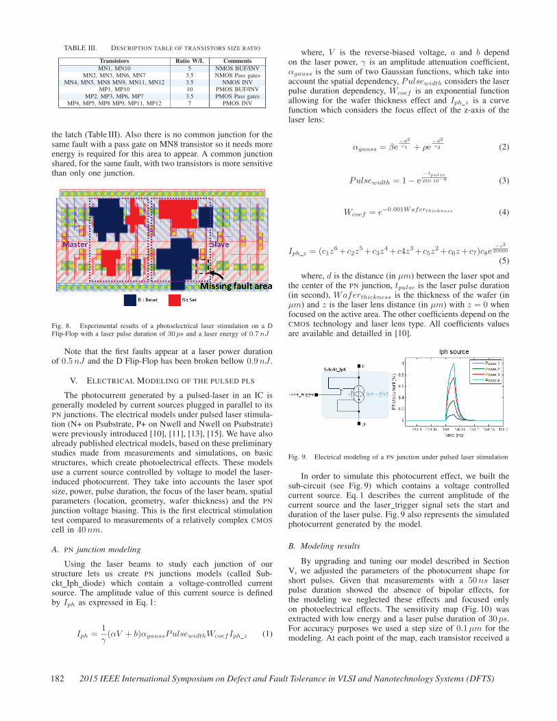
TABLE III. DESCRIPTION TABLE OF TRANSISTORS SIZE RATIO
Transistors Ratio W/L CommentsMN1, MN10 5 NMOS BUF/INV
MN2, MN3, MN6, MN7 3.5 NMOS Pass gatesMN4, MN5, MN8 MN9, MN11, MN12 3.5 NMOS INV
MP1, MP10 10 PMOS BUF/INVMP2, MP3, MP6, MP7 3.5 PMOS Pass gates
MP4, MP5, MP8 MP9, MP11, MP12 7 PMOS INV
the latch (Table III). Also there is no common junction for thesame fault with a pass gate on MN8 transistor so it needs moreenergy is required for this area to appear. A common junctionshared, for the same fault, with two transistors is more sensitivethan only one junction.
Fig. 8. Experimental results of a photoelectrical laser stimulation on a DFlip-Flop with a laser pulse duration of 30 ps and a laser energy of 0.7nJ
Note that the first faults appear at a laser power durationof 0.5nJ and the D Flip-Flop has been broken bellow 0.9nJ .
V. ELECTRICAL MODELING OF THE PULSED PLS
The photocurrent generated by a pulsed-laser in an IC isgenerally modeled by current sources plugged in parallel to itsPN junctions. The electrical models under pulsed laser stimula-tion (N+ on Psubstrate, P+ on Nwell and Nwell on Psubstrate)were previously introduced [10], [11], [13], [15]. We have alsoalready published electrical models, based on these preliminarystudies made from measurements and simulations, on basicstructures, which create photoelectrical effects. These modelsuse a current source controlled by voltage to model the laser-induced photocurrent. They take into accounts the laser spotsize, power, pulse duration, the focus of the laser beam, spatialparameters (location, geometry, wafer thickness) and the PNjunction voltage biasing. This is the first electrical stimulationtest compared to measurements of a relatively complex CMOScell in 40nm.
A. PN junction modeling
Using the laser beams to study each junction of ourstructure lets us create PN junctions models (called Sub-ckt Iph diode) which contain a voltage-controlled currentsource. The amplitude value of this current source is definedby Iph as expressed in Eq. 1:
Iph =1
γ(αV + b)αgaussPulsewidthWcoefIph z (1)
where, V is the reverse-biased voltage, a and b dependon the laser power, γ is an amplitude attenuation coefficient,αgauss is the sum of two Gaussian functions, which take intoaccount the spatial dependency, Pulsewidth considers the laserpulse duration dependency, Wcoef is an exponential functionallowing for the wafer thickness effect and Iph z is a curvefunction which considers the focus effect of the z-axis of thelaser lens:
αgauss = βe−d2
c1 + ρe−d2
c2 (2)
Pulsewidth = 1− e−tpulse
250.10−9 (3)
Wcoef = e−0.001Waferthickness (4)
Iph z = (c1z6+ c2z
5+ c3z4+ c4z3+ c5z
2+ c6z+ c7)c8e−z2
20000
(5)
where, d is the distance (in µm) between the laser spot andthe center of the PN junction, tpulse is the laser pulse duration(in second), Waferthickness is the thickness of the wafer (inµm) and z is the laser lens distance (in µm) with z = 0 whenfocused on the active area. The other coefficients depend on theCMOS technology and laser lens type. All coefficients valuesare available and detailled in [10].
Fig. 9. Electrical modeling of a PN junction under pulsed laser stimulation
In order to simulate this photocurrent effect, we built thesub-circuit (see Fig. 9) which contains a voltage controlledcurrent source. Eq. 1 describes the current amplitude of thecurrent source and the laser trigger signal sets the start andduration of the laser pulse. Fig. 9 also represents the simulatedphotocurrent generated by the model.
B. Modeling results
By upgrading and tuning our model described in SectionV, we adjusted the parameters of the photocurrent shape forshort pulses. Given that measurements with a 50ns laserpulse duration showed the absence of bipolar effects, forthe modeling we neglected these effects and focused onlyon photoelectrical effects. The sensitivity map (Fig. 10) wasextracted with low energy and a laser pulse duration of 30 ps.For accuracy purposes we used a step size of 0.1µm for themodeling. At each point of the map, each transistor received a
182 2015 IEEE International Symposium on Defect and Fault Tolerance in VLSI and Nanotechnology Systems (DFTS)
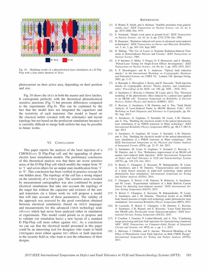
Fig. 10. Modeling results of a photoelectrical laser stimulation on a D Flip-Flop with a laser pulse duration of 30 ps
photocurrent on their active area, depending on their positionand size.
Fig. 10 shows the SEUs in both the master and slave latches.It corresponds perfectly with the theoretical photoelectricalsensitive junctions (Fig. 7) but presents differences comparedto the experiments (Fig. 8). This can be explained by thefact that the model does not integrated the capacitors andthe resistivity of each transistor. Our model is based onthe classical netlist (created with the schematic) and layouttopology but not based on the postlayout simulations because itis currently difficult to merge both netlists but may be possiblein future works.
VI. CONCLUSION
This paper reports the analysis of the laser injection of aCMOS40nm D Flip-Flop cell and the upgrading of photo-electric laser stimulation models. The preliminary conclusionof this theoretical analyze was that there are seven sensitiveareas of the D Flip-Flop cell which modify the output from ‘0’to ‘1’ and seven others for an output state modification from ‘1’to ‘0’. This conclusion has been verified in practice (except forone hidden area). The topology of the cell has a strong impacton the sensitivity of a CMOS gate. The sensitive areas revealedby measurement cartographies was also confirmed by properelectrical simulations that take into account the topology ofthe target but without the capacitor and resistors of the netsand transistors (in a future work we will propose a modelthat will take account of these parameters). The validity ofthe approach was assessed by the good correlation obtainedbetween electrical simulations (based on SPICE language)and measurements for this advanced CMOS technology node(40nm) which had never been analyzed either in simulationor experiments. This model could permit us to propose andto validate (on simulation basis) a new layout of a standardD Flip-Flop cell more robust against SEU. As a conclusionwe can say that the electrical model presented in this papercould be an interesting tool for designers who wants to buildCMOSgates more robust against SEU effects or fault injectionin the security field or, who want to test the robustness of theirdesigns.
REFERENCES
[1] D. Binder, E. Smith, and A. Holman, “Satellite anomalies from galacticcosmic rays,” IEEE Transactions on Nuclear Science, vol. 22, no. 6,pp. 2675–2680, Dec 1975.
[2] E. Normand, “Single event upset at ground level,” IEEE Transactionson Nuclear Science, vol. 43, no. 6, pp. 2742–2750, Dec 1996.
[3] R. Baumann, “Radiation-induced soft errors in advanced semiconductortechnologies,” IEEE Transactions on Device and Materials Reliability,vol. 5, no. 3, pp. 305–316, Sept 2005.
[4] D. Habing, “The Use of Lasers to Simulate Radiation-Induced Tran-sients in Semiconductor Devices and Circuits,” IEEE Transactions onNuclear Science, 1965.
[5] S. P. Buchner, F. Miller, V. Pouget, D. P. Mcmorrow, and S. Member,“Pulsed-Laser Testing for Single-Event Effects Investigations,” IEEETransactions on Nuclear Science, vol. 60, no. 3, pp. 1852–1875, 2013.
[6] S. P. Skorobogatov and R. J. Anderson, “Optical fault inductionattacks,” in 4th International Workshop on Cryptographic Hardwareand Embedded Systems, ser. CHES ’02. London, UK: Springer-Verlag,2002, pp. 2–12.
[7] A. Barenghi, L. Breveglieri, I. Koren, and D. Naccache, “Fault injectionattacks on cryptographic devices: Theory, practice, and countermea-sures,” Proceedings of the IEEE, vol. 100, pp. 3056 – 3076, 2012.
[8] A. Sarafianos, C. Roscian, J. Dutertre, M. Lisart, and A. Tria, “Electricalmodeling of the photoelectric effect induced by a pulsed laser appliedto an SRAM cell,” European Symposium on Reliability of ElectronDevices, Failure Physics and Analysis (ESREF), 2013.
[9] C. Roscian, A. Sarafianos, J.-M. Dutertre, and A. Tria, “Fault ModelAnalysis of Laser-Induced Faults in SRAM Memory Cells,” 2013Workshop on Fault Diagnosis and Tolerance in Cryptography, pp. 89–98, Aug. 2013.
[10] A. Sarafianos, O. Gagliano, V. Serradeil, M. Lisart, J.-M. Dutertre,and A. Tria, “Building the electrical model of the pulsed photoelectriclaser stimulation of an NMOS transistor in 90nm technology,” IEEEInternational Reliability Physics Symposium (IRPS), pp. 5B.5.1–5B.5.9,Apr. 2013.
[11] A. Sarafianos, O. Gagliano, M. Lisart, V. Serradeil, J.-M. Dutertre,and A. Tria, “Building the electrical model of the pulsed photoelectriclaser stimulation of a PMOS transistor in 90nm technology,” 20thIEEE International Symposium on the Physical and Failure Analysisof Integrated Circuits (IPFA), pp. 22–27, Jul. 2013.
[12] A. Sarafianos, M. Lisart, O. Gagliano, V. Serradeil, C. Roscian, J.-M. Dutertre, and A. Tria, “Robustness improvement of an SRAM cellagainst laser-induced fault injection,” IEEE International Symposiumon Defect and Fault Tolerance in VLSI and Nanotechnology Systems(DFTS), pp. 149–154, Oct. 2013.
[13] N. Borrel, C. Champeix, E. Kussener, W. Rahajandraibe, W. Lisart,A. Sarafianos, and J. M. Dutertre, “Characterization and simulationof a body biased structure in triple-well technology under pulsedphotoelectric laser stimulation,” International Symposium for Testingand Failure Analysis (ISTFA), 2014.
[14] C. Champeix, N. Borrel, J.-M. Dutertre, B. Robisson, A. Sarafianos,and M. Lisart, “Experimental validation of a Bulk Built-In CurrentSensor for detecting laser-induced currents,” IEEE International On-Line Testing Symposium (IOLTS), 2015.
[15] N. Borrel, C. Champeix, E. Kussener, W. Rahajandraibe, W. Lisart,A. Sarafianos, and J. M. Dutertre, “Electrical model of an NMOSbody biased structure in triple-well technology under photoelectric laserstimulation,” International Reliability Physics Symposium (IRPS), 2015.
[16] M. Lacruche, N. Borrel, C. Champeix, J.-M. Dutertre, C. Roscian,A. Sarafianos, J.-B. Rigaud, and E. Kussener, “Laser Fault Injectioninto SRAM cells: Picosecond versus Nanosecond pulses,” IEEE Inter-national On-Line Testing Symposium (IOLTS), 2015.
[17] F. Courbon, J. Fournier, P. Loubet-Moundi, and A. Tria, “Combiningimage processing and laser fault injections for characterizing a hardwareAES,” IEEE Transactions on Computer-Aided Design of IntegratedCircuits and Systems, vol. 0070, no. c, pp. 1–1, 2015.
[18] L. Herivaux, J. Clediere, and S. Anceau, “Electrical Modeling of theEffect of Photoelectric Laser Fault Injection on Bulk CMOS Design,”International Symposium for Testing and Failure Analysis (ISTFA),2013.
2015 IEEE International Symposium on Defect and Fault Tolerance in VLSI and Nanotechnology Systems (DFTS) 183


![The Story of Picosecond Ultrasonicsperso.univ-lemans.fr/~pruello/Picosecond ultrasonics from lab to... · The Story of Picosecond Ultrasonics 1 Christopher Morath, ... [ps] 0.00 0.05](https://img.dokumen.tips/doc/110x75/5a8820a97f8b9aa5408e58d4/the-story-of-picosecond-pruellopicosecond-ultrasonics-from-lab-tothe-story-of.jpg)