Embed Size (px)
Citation preview
SERVICE MANUAL
DATA
BASIC CD MECHANISM : DA11T3COMPACT DISCSTEREO CASSETTE RECODER
CSD-A280
S/M Code No. 09-002-430-0R1
LH
REVISION
This Service Manual is the "Revision Publishing" and replaces "Simple Manual"
(S/M Code No. 09-002-430-0T1).
BASIC TAPE MECHANISM : TN-21ZVC-2000
2
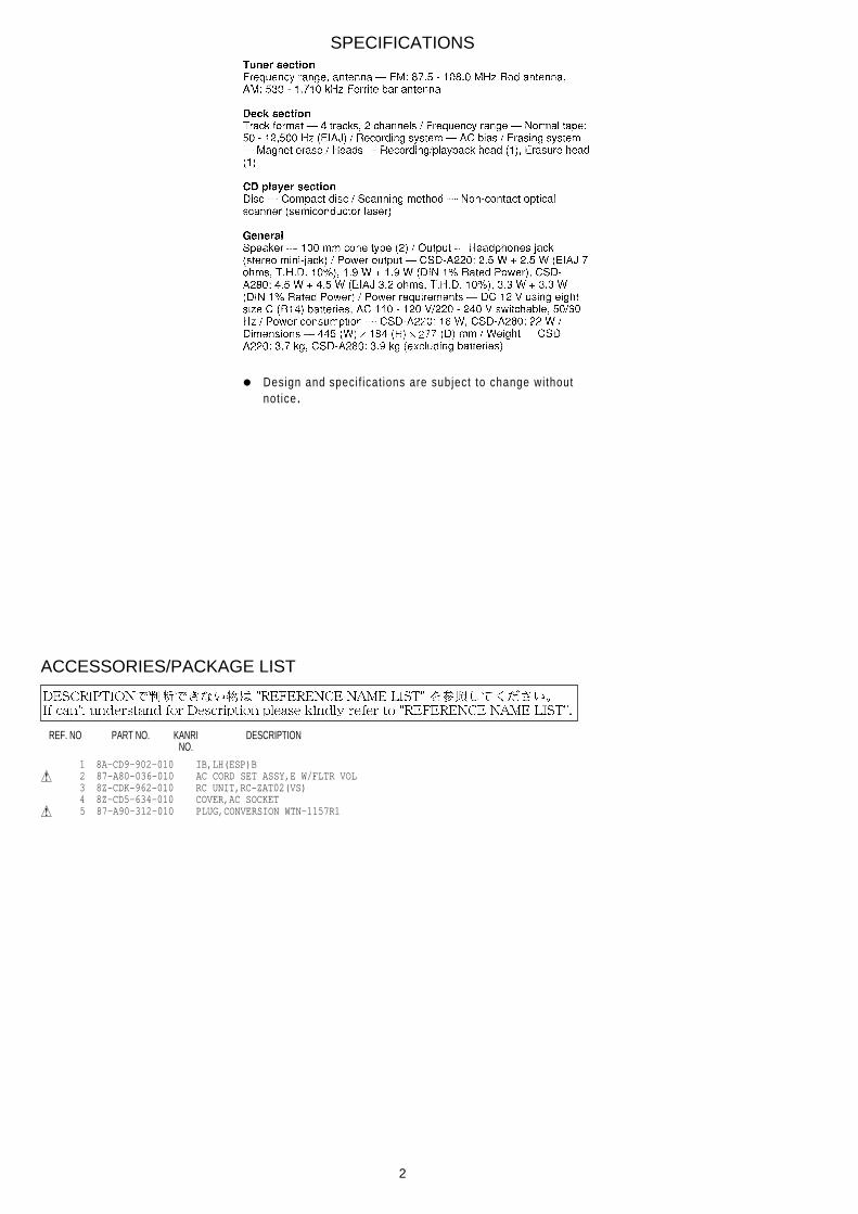
SPECIFICATIONS
REF. NO PART NO. KANRI DESCRIPTIONNO.
ACCESSORIES/PACKAGE LIST
• Design and specif icat ions are subject to change withoutnot ice.
1 8A-CD9-902-010 IB,LH(ESP)B! 2 87-A80-036-010 AC CORD SET ASSY,E W/FLTR VOL 3 8Z-CDK-962-010 RC UNIT,RC-ZAT02(VS) 4 8Z-CD5-634-010 COVER,AC SOCKET! 5 87-A90-312-010 PLUG,CONVERSION WTN-1157R1
3
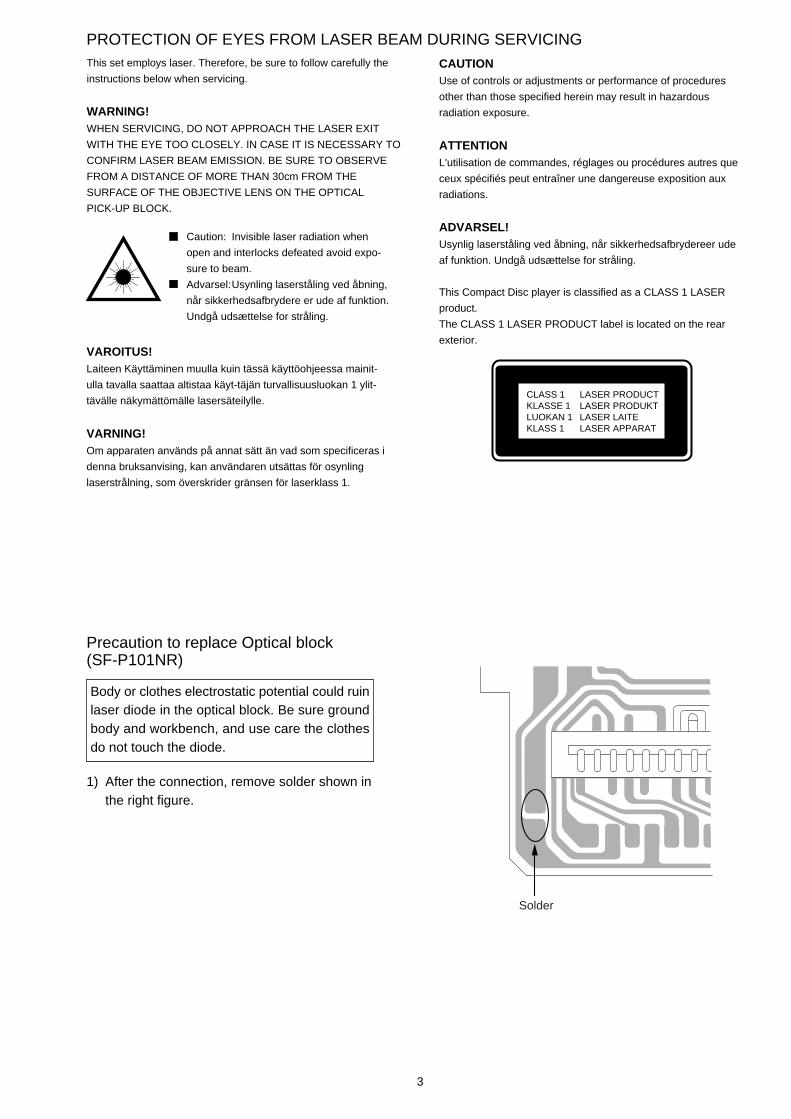
PROTECTION OF EYES FROM LASER BEAM DURING SERVICING
VAROITUS!Laiteen Käyttäminen muulla kuin tässä käyttöohjeessa mainit-
ulla tavalla saattaa altistaa käyt-täjän turvallisuusluokan 1 ylit-
tävälle näkymättömälle lasersäteilylle.
VARNING!Om apparaten används på annat sätt än vad som specificeras i
denna bruksanvising, kan användaren utsättas för osynling
laserstrålning, som överskrider gränsen för laserklass 1.
Caution: Invisible laser radiation when
open and interlocks defeated avoid expo-
sure to beam.
Advarsel:Usynling laserståling ved åbning,
når sikkerhedsafbrydere er ude af funktion.
Undgå udsættelse for stråling.
CAUTIONUse of controls or adjustments or performance of procedures
other than those specified herein may result in hazardous
radiation exposure.
ATTENTIONL'utilisation de commandes, réglages ou procédures autres que
ceux spécifiés peut entraîner une dangereuse exposition aux
radiations.
ADVARSEL!Usynlig laserståling ved åbning, når sikkerhedsafbrydereer ude
af funktion. Undgå udsættelse for stråling.
This Compact Disc player is classified as a CLASS 1 LASER
product.
The CLASS 1 LASER PRODUCT label is located on the rear
exterior.
This set employs laser. Therefore, be sure to follow carefully the
instructions below when servicing.
WARNING!WHEN SERVICING, DO NOT APPROACH THE LASER EXIT
WITH THE EYE TOO CLOSELY. IN CASE IT IS NECESSARY TO
CONFIRM LASER BEAM EMISSION. BE SURE TO OBSERVE
FROM A DISTANCE OF MORE THAN 30cm FROM THE
SURFACE OF THE OBJECTIVE LENS ON THE OPTICAL
PICK-UP BLOCK.
CLASS 1KLASSE 1LUOKAN 1KLASS 1
LASER PRODUCTLASER PRODUKTLASER LAITELASER APPARAT
Precaution to replace Optical block(SF-P101NR)
1) After the connection, remove solder shown inthe right figure.
Body or clothes electrostatic potential could ruinlaser diode in the optical block. Be sure groundbody and workbench, and use care the clothesdo not touch the diode.
Solder

4
T
REF. NO PART NO. KANRI DESCRIPTIONNO.
REF. NO PART NO. KANRI DESCRIPTIONNO.
ELECTRICAL MAIN PARTS LIST
IC
87-A20-955-010 IC,LA1828 87-A21-090-010 IC,LA4600 87-A21-520-040 C-IC,M61509FP 87-A20-446-010 C-IC,LA9241ML 87-A20-459-010 C-IC,LC78622ED
87-A21-093-010 IC,LA6541D 8A-CD9-610-010 C-IC,LC865516A-5916 87-A20-650-010 IC,RPM6938-V11 87-A21-431-010 IC,BA4560N
TRANSISTOR
89-327-143-080 TR,2SC2714 (0.1W) 89-327-125-080 CHIP TR,2SC2712GR 87-026-230-080 CHIP-TR,DTA114YK 87-026-213-080 CHIP-TR,DTC114YK 89-318-154-080 TR,2SC1815Y
89-112-965-080 TR,2SA1296 (0.75W) 87-026-463-080 TR,2SA933S (0.3W) 87-026-291-080 TR,DTC124XS 89-213-702-080 TR,2SB1370E 87-026-462-080 TR,2SC1740 S(RS 0.3W)
89-109-332-380 TR,2SA933RS 89-113-187-080 TR,2SA1318TU 87-026-295-080 TR,DTC144TK 87-026-237-080 CHIP-TR,DTC124XK 89-317-403-080 TR,2SC1740S
87-026-464-010 TR,DTC114TS 87-026-464-080 TR,DTC114TS (0.3W)
DIODE
87-020-465-080 DIODE,1SS133 (110MA) 87-027-607-080 ZENER,HZ7B3L 87-070-345-080 DIODE,1N4148 87-A40-648-080 ZENER,MTZJ8.2A 87-A40-234-080 ZENER,MTZJ5.6A
87-017-978-080 DIODE,1N4003 87-027-702-080 DIODE,ZENER HZ6C2L (200MA) 87-A40-465-010 DIODE,FR202
MAIN C.B
C211 87-010-805-080 C-CAP,S 0.15-50 M F C212 87-010-805-080 C-CAP,S 0.15-50 M F C215 87-016-460-080 C-CAP,S 0.22-16 B C216 87-016-460-080 C-CAP,S 0.22-16 B C231 87-010-213-080 C-CAP,S 0.015-50 B
C232 87-010-213-080 C-CAP,S 0.015-50 B C233 87-A10-201-080 C-CAP,S0.33-16 KB C234 87-A10-201-080 C-CAP,S0.33-16 KB C235 87-016-669-080 C-CAP,S 0.1-25 K B C236 87-016-669-080 C-CAP,S 0.1-25 K B
C237 87-010-408-080 CAP,E 470-6.3 M SME C239 87-010-197-080 CAP, CHIP 0.01 DM C240 87-010-197-080 CAP, CHIP 0.01 DM C247 87-010-401-080 CAP.E 1-50 M 11L SME C248 87-010-401-080 CAP,E 1-50 M 11L SME
C310 87-010-248-080 CAP, ELECT 220-10V C316 87-010-263-080 CAP,E 100-10 M 11L SME C317 87-015-819-080 C-CAP,0.01-50 K B C3216 C801 87-010-248-080 CAP, ELECT 220-10V C805 87-012-365-080 C-CAP,S 0.027-25VBK
C806 87-012-365-080 C-CAP,S 0.027-25VBK C807 87-010-405-080 CAP, ELECT 10-50V C808 87-010-405-080 CAP, ELECT 10-50V C809 87-010-405-080 CAP, ELECT 1-50V C810 87-010-405-080 CAP, ELECT 1-50V
C811 87-010-178-080 CHIP CAP 1000P C812 87-010-178-080 CHIP CAP 1000P C816 87-010-180-080 C-CER 1500P C817 87-010-180-080 C-CER 1500P C821 87-010-401-080 CAP, ELECT 1-50V
C822 87-010-401-080 CAP, ELECT 1-50V C823 87-010-178-080 CHIP CAP 1000P C824 87-010-178-080 CHIP CAP 1000P C829 87-010-178-080 CHIP CAP 1000P C830 87-010-178-080 CHIP CAP 1000P
C833 87-018-195-080 CAP, CER 1200P-16V C834 87-010-248-080 CAP, ELECT 220-10V C835 87-010-322-080 C-CAP,S 100P-50 CH C836 87-010-322-080 C-CAP,S 100P-50 CH C843 87-010-197-080 CAP, CHIP 0.01 DM
C844 87-018-124-080 CAP, CER 270P-50V C845 87-010-178-080 CHIP CAP 1000P C846 87-010-263-080 CAP, ELECT 100-10V C851 87-010-186-080 CAP,CHIP 4700P C852 87-010-178-080 CHIP CAP 1000P
C853 87-A11-145-080 CAP,TC U 0.01-50 Z F CN201 87-099-018-010 CONN,16P CN801 87-A60-110-010 CONN,4P V S2M-4W CNA302 8A-CD9-629-010 CONN ASSY,6P MA-TU L801 87-007-342-010 COIL,OSC 85K BIAS
SP904 87-CD6-213-010 SPR-C,BATT (-) SW801 8Z-CD9-609-010 SW,SL 1-6-2 PS62D01
CD C.B
C30 87-010-260-080 CAP, ELECT 47-25V C251 87-010-404-080 CAP.E 4.7-50 M 11L SME C263 87-010-178-080 CHIP CAP 1000P C264 87-010-178-080 CHIP CAP 1000P C266 87-010-545-080 CAP, ELECT 0.22-50V
C267 87-010-545-080 CAP, ELECT 0.22-50V C271 87-010-237-080 CAP, ELECT 1000-16V C272 87-010-237-080 CAP, ELECT 1000-16V C277 87-010-404-080 CAP, ELECT 4.7-50V C278 87-010-263-080 CAP, ELECT 100-10V
C279 87-010-263-080 CAP, ELECT 100-10V C301 87-016-495-000 CAP,E 3300-25 M SMG C302 87-010-265-080 CAP,E 33-16 M 11L SME C306 87-010-404-080 CAP, ELECT 4.7-50V C307 87-010-401-080 CAP, ELECT 1-50V
C308 87-010-221-080 CAP, ELECT 470-10V C311 87-010-374-080 CAP, ELECT 47-10V C312 87-010-385-080 CAP, ELECT 220-25V C321 87-010-197-080 CAP, CHIP 0.01 DM C322 87-010-263-080 CAP, ELECT 100-10V
C325 87-010-405-080 CAP, ELECT 10-50V C401 87-010-403-080 CAP, ELECT 3.3-50V C402 87-010-197-080 CAP, CHIP 0.01 DM C403 87-010-263-080 CAP, ELECT 100-10V C404 87-010-248-080 CAP, ELECT 220-10V
C405 87-010-197-080 CAP, CHIP 0.01 DM C406 87-010-374-080 CAP, ELECT 47-10V C407 87-010-178-080 CHIP CAP 1000P C408 87-010-198-080 CAP, CHIP 0.022 C409 87-010-248-080 CAP, ELECT 220-10V
C410 87-010-263-080 CAP, ELECT 100-10V C411 87-A11-177-080 C-CAP,S 0.15-16 K B C412 87-010-401-080 CAP, ELECT 1-50V C413 87-016-369-080 C-CAP,S 0.033-25 B K C414 87-010-405-080 CAP, ELECT 10-50V
C416 87-010-545-080 CAP, ELECT 0.22-50V C417 87-012-157-080 C-CAP,S 330P-50 CH C418 87-010-213-080 C-CAP,S 0.015-50 B C419 87-A11-608-080 C-CAP,S 0.33-25 K B C420 87-016-369-080 C-CAP,S 0.033-25 B K

5
REF. NO PART NO. KANRI DESCRIPTIONNO.
REF. NO PART NO. KANRI DESCRIPTIONNO.
C421 87-A11-177-080 C-CAP,S 0.15-16 K B C422 87-010-184-080 CHIP CAPACITOR 3300P(K) C423 87-010-992-080 C-CAP,S 0.047-25 B C424 87-016-460-080 C-CAP,S 0.22-16 B C425 87-010-176-080 C-CAP,S 680P-50 SL
C426 87-A11-608-080 C-CAP,S 0.33-25 K B C428 87-010-197-080 CAP, CHIP 0.01 DM C429 87-010-186-080 CAP,CHIP 4700P C430 87-012-156-080 C-CAP,S 220P-50 CH C431 87-010-545-080 CAP, ELECT 0.22-50V
C432 87-010-374-080 CAP, ELECT 47-10V C433 87-010-401-080 CAP, ELECT 1-50V C434 87-010-184-080 CHIP CAPACITOR 3300P(K) C435 87-010-197-080 CAP, CHIP 0.01 DM C436 87-010-374-080 CAP, ELECT 47-10V
C437 87-010-404-080 CAP, ELECT 4.7-50V C438 87-016-669-080 C-CAP,S 0.1-25 K B C439 87-010-178-080 CHIP CAP 1000P C440 87-010-145-080 C-CAP,S 1P-50 C CH GRM C441 87-010-197-080 CAP, CHIP 0.01 DM
C442 87-010-313-080 CAP, CHIP 18P C445 87-012-368-080 C-CAP,S 0.1-50 F C446 87-012-368-080 C-CAP,S 0.1-50 F C447 87-012-368-080 C-CAP,S 0.1-50 F C448 87-010-315-080 C-CAP,S 27P-50 CH
C450 87-012-140-080 CAP 470P C451 87-012-156-080 C-CAP,S 220P-50 CH C455 87-010-247-080 CAP, ELECT 100-50V C457 87-010-312-080 C-CAP,S 15P-50 CH C458 87-010-312-080 C-CAP,S 15P-50 CH
C459 87-010-263-080 CAP, ELECT 100-10V C460 87-015-819-080 CAPACITOR,0.01 C461 87-010-197-080 CAP, CHIP 0.01 DM C462 87-010-248-080 CAP, ELECT 220-10V C463 87-010-197-080 CAP, CHIP 0.01 DM
C465 87-010-404-080 CAP, ELECT 4.7-50V C466 87-012-368-080 C-CAP,S 0.1-50 F C467 87-010-263-080 CAP, ELECT 100-10V C469 87-012-154-080 C-CAP,S 150P-50 CH C470 87-010-544-080 CAP, ELECT 0.1-50V
C471 87-015-785-080 CHIP CAPACITOR, 0.1FZ-25Z C472 87-015-785-080 CHIP CAPACITOR, 0.1FZ-25Z C473 87-015-785-080 CHIP CAPACITOR, 0.1FZ-25Z C474 87-015-785-080 CHIP CAPACITOR, 0.1FZ-25Z C475 87-010-197-080 CAP, CHIP 0.01 DM
C476 87-010-236-080 CAP,E 1000-10 SME C477 87-010-197-080 CAP, CHIP 0.01 DM C478 87-010-263-080 CAP, ELECT 100-10V C479 87-010-197-080 CAP, CHIP 0.01 DM C480 87-010-221-080 CAP, ELECT 470-10V
C481 87-010-405-080 CAP, ELECT 10-50V C482 87-010-405-080 CAP, ELECT 10-50V C489 87-012-368-080 C-CAP,S 0.1-50 F C490 87-012-368-080 C-CAP,S 0.1-50 F C491 87-010-197-080 CAP, CHIP 0.01 DM
C492 87-010-221-080 CAP, ELECT 470-10V C493 87-010-180-080 C-CAP,S 1500P-50 K B C2012 C494 87-010-197-080 CAP, CHIP 0.01 DM C501 87-012-368-080 C-CAP,S 0.1-50 F C502 87-010-322-080 C-CAP,S 100P-50 CH
C503 87-010-322-080 C-CAP,S 100P-50 CH C504 87-010-322-080 C-CAP,S 100P-50 CH C505 87-010-322-080 C-CAP,S 100P-50 CH C506 87-010-322-080 C-CAP,S 100P-50 CH C510 87-016-669-080 C-CAP,S 0.1-25 K B
C831 87-010-198-080 CAP, CHIP 0.022 CN202 8A-CH4-689-010 CONN,3P V 2.5 CN205 87-A60-109-010 CONN,2P V S2M-2W CN301 8A-CH4-689-010 CONN,3P V 2.5 CN401 87-A60-424-010 CONN,16P V TOC-B
CN403 87-099-201-010 CONN,8P 6216 H CN802 8A-CH4-687-010 CONN,4P V 2.5 CNA402 8A-CD9-625-010 CONN ASSY,6P CD-ME L401 87-003-102-080 COIL, 10UH L404 87-003-152-080 COIL, 100UH
R840 87-029-124-010 RES,FUSE 2.2-1/4 SFR430 87-024-437-080 SFR100K,RH063EC X401 8Z-CD5-633-010 VIB, CER16.93MHZ FCR16.93M2
FRONT C.B
C601 87-010-313-080 CAP, CHIP 18P C602 87-010-315-080 C-CAP,S 27P-50 CH C603 87-010-319-080 C-CAP,S 56P-50 CH C604 87-010-317-010 CHIP CAP,S 39P CH C605 87-010-264-040 CAP,E 100-10 5L
C606 87-010-805-080 CAP, S 1-16 C607 87-010-452-080 CAPACITOR,1-16 C608 87-010-405-080 CAP, ELECT 10-50V C609 87-010-400-080 CAP, ELECT 0.47-50V C610 87-010-178-010 CAP, S 1000P-50
C611 87-A10-189-040 CAP,E 220-10 C612 87-010-405-080 CAP, ELECT 10-50V C613 87-012-368-080 C-CAP,S 0.1-50 F C614 87-010-312-080 C-CAP,S 15P-50 CH C615 87-010-805-080 CAP, S 1-16
C616 87-010-805-080 CAP, S 1-16 C619 87-010-401-080 CAP,ELECT 1-50V C635 87-018-211-080 CAP,TC U 0.01-50 Z F SA CN601 87-099-033-010 16P 6216 H CN602 87-099-201-010 CONN,8P 6216 H
CN604 8A-CD9-623-010 CONN ASSY,4P KEY JW132 87-003-098-080 COIL,2.2UH JW133 87-003-098-080 COIL,2.2UH L603 87-003-098-080 COIL,2.2UH L604 87-003-098-080 COIL,2.2UH
L605 87-003-098-080 COIL,2.2UH L606 87-003-098-080 COIL,2.2UH L607 87-003-098-080 COIL,2.2UH L608 87-003-098-080 COIL,2.2UH L609 87-003-098-080 COIL,2.2UH
LED602 88-CD6-630-010 LED,934ID RED LED603 88-CD6-630-010 LED,934ID RED LED606 88-CD6-630-010 LED,934ID RED LED607 88-CD6-630-010 LED,934ID RED LED608 88-CD6-630-010 LED,934ID RED
LED610 88-CD6-631-010 LED,934GD GRN LED611 87-CD8-616-010 LED,SA36-11 HWA-11.0 S601 87-A91-704-080 SW,TACT EVQ 214 05R S602 87-A91-704-080 SW,TACT EVQ 214 05R S603 87-A91-704-080 SW,TACT EVQ 214 05R
S604 87-A91-704-080 SW,TACT EVQ 214 05R S605 87-A91-704-080 SW,TACT EVQ 214 05R S609 87-A91-704-080 SW,TACT EVQ 214 05R S611 87-A91-704-080 SW,TACT EVQ 214 05R X601 87-030-273-010 VIB,XTAL 32.768K5PPM
X602 87-030-376-080 VIB,CER CSA5.76MG200
TUNER C.B
C1 87-010-314-080 C-CAP,S 22P-50V C2 87-010-318-080 C-CAP,S 47P-50 CH C3 87-010-317-080 C-CAP,S 39P-50 CH C4 87-010-148-080 CAP, 4P-50 C CH GRM C5 87-010-378-080 CAP, ELECT 10-16V
C6 87-010-378-080 CAP, ELECT 10-16V C7 87-018-208-080 CAP 0.047-50F C8 87-010-197-080 CAP, CHIP 0.01 DM C9 87-010-154-080 CAP CHIP 10P C10 87-010-197-080 CAP, CHIP 0.01 DM

6
REF. NO PART NO. KANRI DESCRIPTIONNO.
REF. NO PART NO. KANRI DESCRIPTIONNO.
C11 87-010-154-080 CAP CHIP 10P C12 87-010-314-080 C-CAP,S 22P-50V C13 87-010-148-080 C-CAP,S 4P-50 C CH GRM C14 87-012-141-080 0.01-25 K B C2012 C15 87-010-197-080 C-CAP,S0.01-25 K B C 2012
C16 87-010-178-080 CHIP CAP 1000P C17 87-016-669-080 C-CAP,S 0.1-25 K B C18 87-010-197-080 CAP, CHIP 0.01 DM C19 87-010-196-080 CHIP CAPACITOR,0.1-25 C20 87-010-400-080 CAP, ELECT 0.47-50V
C21 87-010-403-080 CAP, ELECT 3.3-50V C22 87-010-197-080 CAP, CHIP 0.01 DM C24 87-010-197-080 CAP, CHIP 0.01 DM C25 87-010-197-080 CAP, CHIP 0.01 DM C26 87-012-141-080 CHIP-CAPACITOR,0.22-16F
C27 87-012-141-080 CHIP-CAPACITOR,0.22-16F C28 87-010-992-080 C-CAP,S 0.047-25 B C29 87-010-992-080 C-CAP,S 0.047-25 B C30 87-010-248-080 CAP, ELECT 220-10V C31 87-010-379-080 CAP, ELECT 22-16V
C32 87-010-197-080 CAP, CHIP 0.01 DM C33 87-010-197-080 CAP, CHIP 0.01 DM C34 87-010-197-080 CAP, CHIP 0.01 DM C35 87-010-197-080 CAP, CHIP 0.01 DM C36 87-010-263-080 CAP,ELECT 100-10V
C37 87-012-155-080 C-CAP 180P-50CH C39 87-010-197-080 CAP, CHIP 0.01 DM C51 87-010-197-080 CAP, CHIP 0.01 DM C56 87-010-152-080 C-CAP,S 8P-50 CH CF1 87-A90-128-010 FLTR,AM IF CFAL-455
CF2 87-008-261-010 FILTER, SFE10.7MA5-A CF3 87-008-261-010 FILTER, SFE10.7MA5-A CN2 87-A60-116-010 CONN,6P HS2M-6WR D13 87-A40-128-080 C-VARI-CAP,HVU202A L2 87-A50-346-010 COIL,FM BPF D
L3 87-A50-350-010 COIL,BAR ANT AMN (COI) L4 87-A50-345-010 COIL,FM RF EX L5 87-A50-342-010 COIL,FM OSC D L6 87-A50-337-010 COIL,AM OSC (TOKO) L7 87-A50-336-010 COIL,AM IFT (TOKO)
L8 87-A50-335-010 COIL,FM IFT (TOKO) L9 87-A50-334-010 COIL,FM DET (TOKO) L10 87-005-849-080 COIL,10UH(CECS) PVC1 87-A91-315-010 TUN-CAP,40P-140P D(TWD) SW1 87-A91-548-010 SW,SL-2-3 SK23E01G06
HP C.B
CN204 87-A60-685-010 CONN,4P H WHT EH CN605 87-A60-114-010 CONN,4P H S2M-4WR CNA203 8A-CD9-628-010 CONN ASSY,3P MA-HP J251 87-A60-569-010 JACK,HTJ-035-18 S606 87-A91-704-080 SW,TACT EVQ 214 05R
S607 87-A91-704-080 SW,TACT EVQ 214 05R S608 87-A91-704-080 SW,TACT EVQ 214 05R S614 87-A91-704-080 SW,TACT EVQ 214 05R S615 87-A91-704-080 SW,TACT EVQ 214 05R
POWER C.B
C901 87-010-192-080 C-CAP,S 0.022-50 F C902 87-010-192-080 C-CAP,S 0.022-50 F C903 87-010-192-080 C-CAP,S 0.022-50 F C904 87-010-192-080 C-CAP,S 0.022-50 F CNA901 8A-CD9-627-010 CONN ASSY,3P PWR
!PR901 87-A90-092-080 PROTECTOR,2.5A 491 60V
BATT C.B
VOLTAGE C.B
!SW901 87-036-389-010 SW,PUSH 1-1-1 R8120125
MOTOR C.B
M2 9X-262-576-910 MOTOR GEAR ASSY PIN3 91-564-722-110 CONNECTOR 6P SW1 91-572-085-120 LEAF SW

87
BE
C
2SC2714DTC114TKDTC114YKDTC114YSDTC144EK
E C B
2SA12962SA13182SC1815
E C B
2SA933S2SC1740SDTC114TSDTC124XS
B C E
2SB1370
8 8
A
Resistor Code
Chip Resistor Part Coding
Figure
Value of resistor
Chip resistor
Wattage Type Tolerance
1/16W
1/10W
1/8W
1608
2125
3216
5%
5%
5%
CJ
CJ
CJ
Form L W t
1.6 0.8 0.45
2 1.25 0.45
3.2 1.6
108
118
128
: A : A
CHIP RESISTOR PART CODE
0.55
Resistor CodeDimensions (mm)
Symbol
1/16W 1005 5% CJ 1.0 0.5 0.35 104L
t
W
• Regarding connectors, they are not stocked as they are not the initial order items.The connectors are available after they are supplied from connector manufacturers upon the order is received.
TRANSISTOR ILLUSTRATION
IC BLOCK DIAGRAMIC, LA1828
IC, M61509FP IC, LA6541D

1 2 3 4 5 6 7 8 9 10 11 12 13 14
A
B
C
D
E
F
G
H
I
J
K
109
WIRING-1 (MAIN/CD)
TP3(RF)
TP4(VREF)
TP2(BIAS)

1211
SCHEMATIC DIAGRAM-1 (MAIN/CD 1/2/H.P./POWER)
1413
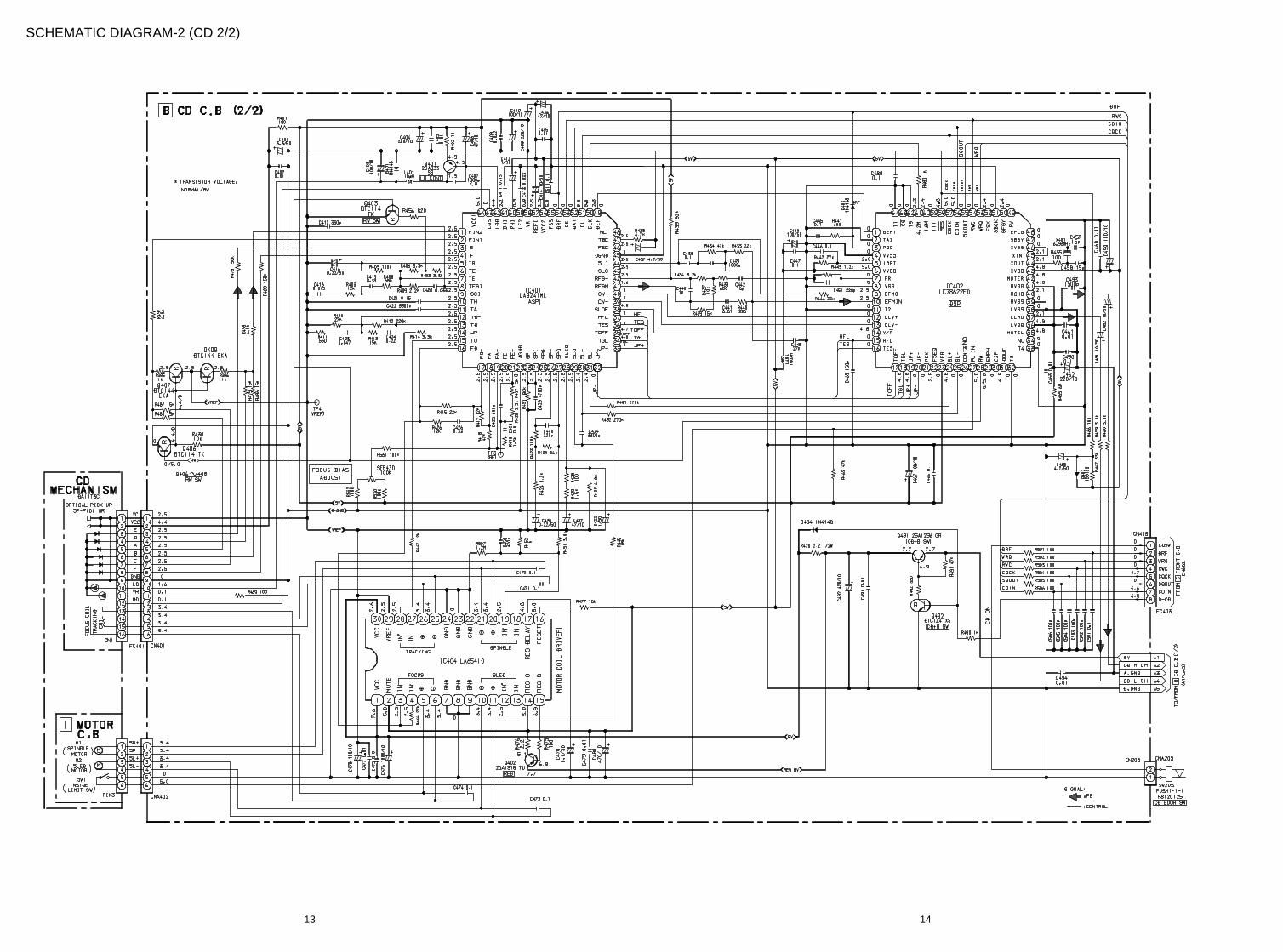
SCHEMATIC DIAGRAM-2 (CD 2/2)

1 2 3 4 5 6 7 8 9 10 11 12 13 14
A
B
C
D
E
F
G
H
I
J
K
1615
WIRING-2 (FRONT/MOTOR)
1817
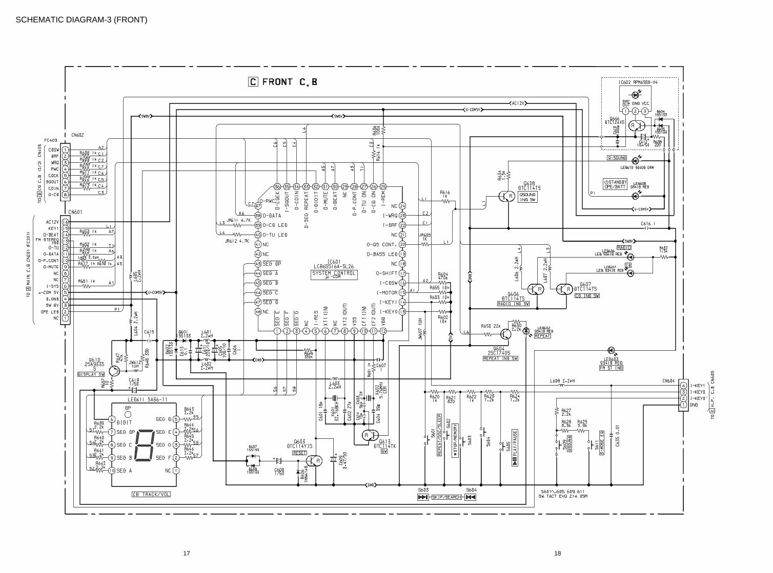
SCHEMATIC DIAGRAM-3 (FRONT)

2019
SCHEMATIC DIAGRAM-4 (TUNER)

2221
1 2 3 4 5 6 7
A
B
C
D
E
F
G
H
I
J
K
WIRING-3 (TUNER)
TP6 (R-CH)
TP5 (L-CH)
AM FM (MONO) FM (ST)
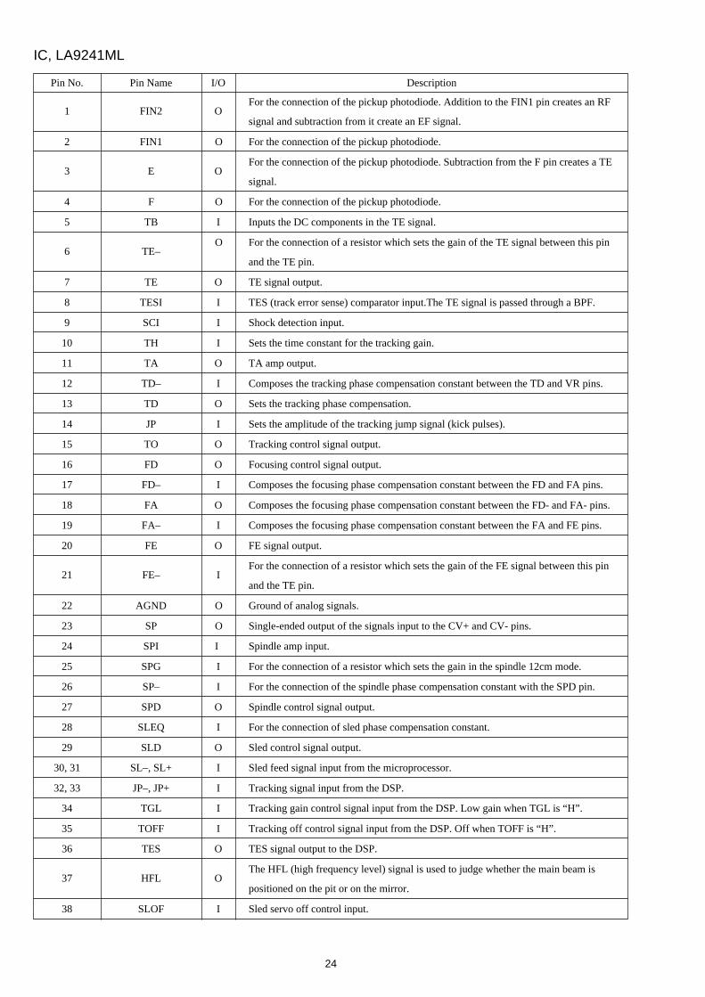
Pin No. Pin Name I/O Description
IC DESCRIPTION
DEFI
TAI
PDO
VVSS
ISET
VVDD
FR
VSS
EFMO
EFMIN
T2
CLV+
CLK-
___
V/P
HFL
TES
TOFF
TGL
JP+
JP-
PCK
FSEQ
VDD
SL+
SL-
CONT3
PUIN
RW
EMPH
C2F
DOUT
T3, T4
N.C.
MUTEL
LVDD
LCHO
I
I
O
—
O
—
I
—
O
I
I
O
O
I
I
O
O
O
O
O
—
O
—
I
O
O
O
O
I
—
O
—
O
Defect detection signal (DEF) input.
Test input. A pull-down resistor is built in. Must be connected to 0V.
External VCO control phase comparator output.
Internal VCO ground. Must be connected to 0V.
PDO output current adjustment resistor connection.
Internal VCO power supply.
VCO frequency range adjustment.
Digital system ground. Must be connected to 0V.
Slice level control; EFM signal output.
Slice level control; EFM signal input.
Test input. A pull-down resistor is built in. Must be connected to 0V.
Disc motor control output.
Three-value ouput is also possible when specified by microprocessor command.
Rough servo/phase control automatic switching monitor output. Outputs a high level
during rough servo and a low level during phase control.
Track detection signal input. This is a Schmitt input.
Tracking error signal input. This is a Schmitt input.
Tracking off output.
Tracking gain switching output. Increase the gain when low.
Track jump output.
Three-value output is also possible when specified by microprocessor command.
EFM data playback clock monitor. Outputs 4.3218 MHz when the phase is locked.
(Not used)
Synchronization signal detection ouput. Outputs a high level when the synchronization
signal detected from the EFM signal and the internally generated synchronization
signal agree. (Not used)
Digital system power supply.
Serial data command sled signal output terminal from microprocessor.
Not used.
CD pickup inside limit switch.
Serial data command sled output terminal from microprocessor.
De-emphasis monitor pin. A high level indicates playback of a de-emphasis disk. (Not
used)
C2 flag output. (Not used)
Digital output (EIAJ format). (Not used)
Test input. A pull-down resistor is built in. Must be connected to 0V.
34Unused. Must be left open.
Left channel one-bit D/A converter mute output. (Not used)
Left channel one-bit D/A converter power supply.
Left channel one-bit D/A converter output.
IC, LC78622ED
1
2
3
4
5
6
7
8
9
10
11
12
13
14
15
16
17
18
19
20
21
22
23
24
25
26
27
28
29
30
31
32, 33
34
35
36
37

23
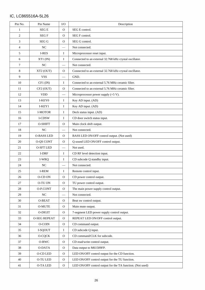
Pin No. Pin Name I/O Description
LVSS
RVSS
RCHO
RVDD
MUTER
XVDD
XOUT
XIN
XVSS
SBSY
EFLG
PW
SFSY
SBCK
FSX
WRQ
RWC
SQOUT
COIN
___________
CQCK
________
RES
T11
16M
4.2M
T5
______
CS
T1
—
—
O
—
O
—
O
I
—
O
O
O
O
I
O
O
I
O
I
I
I
O
O
O
I
I
I
Left channel one-bit D/A converter ground. Must be connected to 0V.
Right channel one-bit D/A converter ground. (Must be connected to 0V.)
Right channel onr-bit D/A converter output.
Right channel one-bit D/A converter power supply.
Right channel one-bit D/A converter mute output. (Not used)
Crystal oscillator power supply.
Connections for a 16.9344 MHz crystal oscillator element.
Crystal oscillator ground. (Must be connected to 0V.)
Subcode clock synchronization signal output. (Not used)
C1, C2, sigle an double error correction monitor. (Not used)
Subcode P, Q, R, S, T, U and W output. (Not used)
Subcode frame synchronization signal output. This signal falls when the subcode arein
standby state. (Not used)
Subcode readout clock input. This is a Schmitt input.
Output pin for the 7.35 kHZ synchronization signal divided from the crystal oscillator.
(Not used)
Subcode Q output standby output.
Read/write control input. This is a Schmitt input.
Subcode Q output.
Command input pin from control microprocessor.
Input for both the command input acquisition clock and the SQOUT pin subcode
readout clock input pin. This is Schmitt input.
Reset input. This pin must be set low briefly after power is first applied.
Test output. Leave open. (Normally output a low level). (Not used)
16.9344 MHz output. (Not used)
4.2336 MHz output.
Test input. A pull-down resistor is built-in. (Must be connected to 0V.)
Chip seledt input. A pull-down resistor is built-in.(Must be connected to 0V if not
controlled.)
Test input. No pull-down resistor. (Must be connected to 0V.)
38
39
40
41
42
43
44
45
46
47
48
49
50
51
52
53
54
55
56
57
58
59
60
61
62
63
64
24
1
2
3
4
5
6
7
8
9
10
11
12
13
14
15
16
17
18
19
20
21
22
23
24
25
26
27
28
29
30, 31
32, 33
34
35
36
37
38
FIN2
FIN1
E
F
TB
TE–
TE
TESI
SCI
TH
TA
TD–
TD
JP
TO
FD
FD–
FA
FA–
FE
FE–
AGND
SP
SPI
SPG
SP–
SPD
SLEQ
SLD
SL–, SL+
JP–, JP+
TGL
TOFF
TES
HFL
SLOF
O
O
O
O
I
O
O
I
I
I
O
I
O
I
O
O
I
O
I
O
I
O
O
I
I
I
O
I
O
I
I
I
I
O
O
I
For the connection of the pickup photodiode. Addition to the FIN1 pin creates an RF
signal and subtraction from it create an EF signal.
For the connection of the pickup photodiode.
For the connection of the pickup photodiode. Subtraction from the F pin creates a TE
signal.
For the connection of the pickup photodiode.
Inputs the DC components in the TE signal.
For the connection of a resistor which sets the gain of the TE signal between this pin
and the TE pin.
TE signal output.
TES (track error sense) comparator input.The TE signal is passed through a BPF.
Shock detection input.
Sets the time constant for the tracking gain.
TA amp output.
Composes the tracking phase compensation constant between the TD and VR pins.
Sets the tracking phase compensation.
Sets the amplitude of the tracking jump signal (kick pulses).
Tracking control signal output.
Focusing control signal output.
Composes the focusing phase compensation constant between the FD and FA pins.
Composes the focusing phase compensation constant between the FD- and FA- pins.
Composes the focusing phase compensation constant between the FA and FE pins.
FE signal output.
For the connection of a resistor which sets the gain of the FE signal between this pin
and the TE pin.
Ground of analog signals.
Single-ended output of the signals input to the CV+ and CV- pins.
Spindle amp input.
For the connection of a resistor which sets the gain in the spindle 12cm mode.
For the connection of the spindle phase compensation constant with the SPD pin.
Spindle control signal output.
For the connection of sled phase compensation constant.
Sled control signal output.
Sled feed signal input from the microprocessor.
Tracking signal input from the DSP.
Tracking gain control signal input from the DSP. Low gain when TGL is “H”.
Tracking off control signal input from the DSP. Off when TOFF is “H”.
TES signal output to the DSP.
The HFL (high frequency level) signal is used to judge whether the main beam is
positioned on the pit or on the mirror.
Sled servo off control input.
IC, LA9241ML
Pin No. Pin Name I/O Description

25
39, 40
41
42
43
44
45
46
47
48
49
50
51
52
53
54
55
56
57
58
59
60
61
62
63
64
CV–, CV+
RFSM
RFS–
SLC
SLI
DGND
FSC
TBC
NC
DEF
CLK
CL
DAT
CE
DRF
FSS
VCC2
REFI
VR
LF2
PH1
BH1
LDD
LDS
VCC1
I
O
O
O
I
—
O
I
—
O
I
I
I
I
O
I
—
—
O
—
—
—
O
I
—
Pin No. Pin Name I/O Description
CLV error signal input from the DSP.
RF output.
Sets the RF gain and the EFM signal’s 3T compensation constant together with the
RFSM pin.
The SLC (slice level control) signal is output to control the DSP’s data slice level of
the RF waveform.
Input to control the DSP’s data slice level.
Ground of digital signals.
Output for the focus search smoothing capacitor.
The TBC (tracking balance control) signal sets the EF balance variation range.
Not connected.
Disc defect detection output.
Reference clock input. 4.23 MHz is input from the DSP.
Microprocessor command clock input.
Microprocessor command data input.
Microprocessor chip enable input.
DRF (detect RF) is an output to detect the RF level.
The FSS (focus search select) signal switches the focus search modes (+/-search /
+search with respect to the reference voltage).
VCC of servo and digital circuits.
For the connection of bypass capacitor for the reference voltage.
Reference voltage output.
Sets the time constant for disc defect detection.
For the connection of a capacitor to hold the RF signal peak.
For the connection of a capacitor to hold the RF signal bottom.
APC circuit output.
APC circuit input.
VCC of RF signal circuits.
26
Pin No. Pin Name I/O Description
1
2
3
4
5
6
7
8
9
10
11
12
13
14
15
16
17
18
19
20
21
22
23
24
25
26
27
28
29
30
31
32
33
34
35
36
37
38
39
40
41
IC, LC865516A-5L26
SEG E
SEG F
SEG G
NC
I-RES
XT1 (IN)
NC
XT2 (OUT)
VSS
CF1 (IN)
CF2 (OUT)
VDD
I-KEY0
I-KEY1
I-MOTOR
I-CDSW
O-SHIFT
NC
O-BASS LED
O-QS CONT
O-SFT LED
I-DRF
I-WRQ
NC
I-REM
O-CD ON
O-TU ON
O-P.CONT
NC
O-BEAT
O-MUTE
O-DIGIT
O-SEG REPEAT
O-COIN
I-SQOUT
O-CQCK
O-RWC
O-DATA
O-CD LED
O-TU LED
O-TA LED
O
O
O
—
I
I
—
O
—
I
O
—
I
I
I
I
O
—
O
O
—
I
I
—
I
O
O
O
—
O
O
O
O
O
I
O
O
O
O
O
O
SEG E control.
SEG F control.
SEG G control.
Not connected.
Microprocessor reset input.
Connected to an external 32.768 kHz crystal oscillator.
Not connected.
Connected to an external 32.768 kHz crystal oscillator.
GND.
Connected to an external 5.76 MHz ceramic filter.
Connected to an external 5.76 MHz ceramic filter.
Microprocessor power supply (+5 V).
Key AD input. (AD)
Key AD input. (AD)
Deck status input. (AD)
CD door switch status input.
Main clock shift output.
Not connected.
BASS LED ON/OFF control output. (Not used)
Q sound LED ON/OFF control output.
Not used.
CD RF level detection input.
CD subcode Q standby input.
Not connected.
Remote control input.
CD power control output.
TU power control output.
The main power supply control output.
Not connected.
Beat sw control output.
Main mute output.
7-segment LED power supply control output.
REPEAT LED ON/OFF control output.
CD command output.
CD subcode Q input.
CD command/CLK for subcode.
CD read/write control output.
Data output to M61509FP.
LED ON/OFF control output for the CD function.
LED ON/OFF control output for the TU function.
LED ON/OFF control output for the TA function. (Not used)

27
Pin No. Pin Name I/O Description
42
43
44
45
46
47
48
NC
SEG DP
SEG A
SEG B
SEG C
SEG D
NC
—
O
O
O
O
O
—
Not connected.
SEG DP control.
SEG A control.
SEG B control.
SEG C control.
SEG D control.
Not connected.

28
ELECTRICAL ADJUSTMENT
< RADIO SECTION >1. AM Frequency Range Adjustment
Settings: • Test Point: TP5 (LCH), TP6 (RCH)• Adjustment location: L006, TC003
L006 ....................................................................... 517kHzTC003 ................................................................... 1750kHz
2. AM Tracking AdjustmentSettings: • Test Point: TP5 (LCH), TP6 (RCH)
• Adjustment location: L003, TC004L003 ....................................................................... 600kHzTC004 ................................................................... 1400kHz
3. AM IF AdjustmentSettings: • Test Point: TP5 (LCH), TP6 (RCH)
• Adjustment location: L007L007 ....................................................................... 455kHz
4. FM Frequency Range AdjustmentSettings: • Test Point: TP5 (LCH), TP6 (RCH)
• Adjustment location: L005, TC001L005 ........................................................................ 87MHzTC001 .................................................................... 109MHz
5. FM Tracking AdjustmentSettings: • Test Point: TP5 (LCH), TP6 (RCH)
• Adjustment location: L004, TC002L004 ........................................................................ 88MHzTC002 .................................................................... 108MHz
6. FM IF AdjustmentSettings: • Test Point: TP5 (LCH), TP6 (RCH)
• Adjustment location: L008, L009L008, L009 ........................................................... 10.7MHz
TC003TC004
TC001
TC002
L009
L007
L008
L004
L006
TP6 (RCH)
IC001
D TUNER C.B
L005
TP5 (LCH)
L003
PVC001
123456
6
3
6
4
1
25
2
29
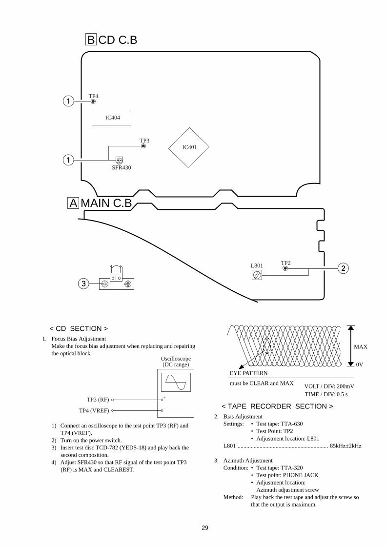
< CD SECTION >1. Focus Bias Adjustment
Make the focus bias adjustment when replacing and repairingthe optical block.
1) Connect an oscilloscope to the test point TP3 (RF) andTP4 (VREF).
2) Turn on the power switch.3) Insert test disc TCD-782 (YEDS-18) and play back the
second composition.4) Adjust SFR430 so that RF signal of the test point TP3
(RF) is MAX and CLEAREST.
< TAPE RECORDER SECTION >2. Bias Adjustment
Settings: • Test tape: TTA-630• Test Point: TP2• Adjustment location: L801
L801 .............................................................. 85kHz±2kHz
3. Azimuth AdjustmentCondition: • Test tape: TTA-320
• Test point: PHONE JACK• Adjustment location:
Azimuth adjustment screwMethod: Play back the test tape and adjust the screw so
that the output is maximum.
L801 TP2
SFR430
TP3
IC404
IC401
TP4
A MAIN C.B
B CD C.B
2
1
1
3
Oscilloscope(DC range)
TP3 (RF)
TP4 (VREF)
EYE PATTERN
must be CLEAR and MAX
MAX
VOLT / DIV: 200mV TIME / DIV: 0.5 s
0V
30
REF. NO PART NO. KANRI DESCRIPTIONNO.
REF. NO PART NO. KANRI DESCRIPTIONNO.
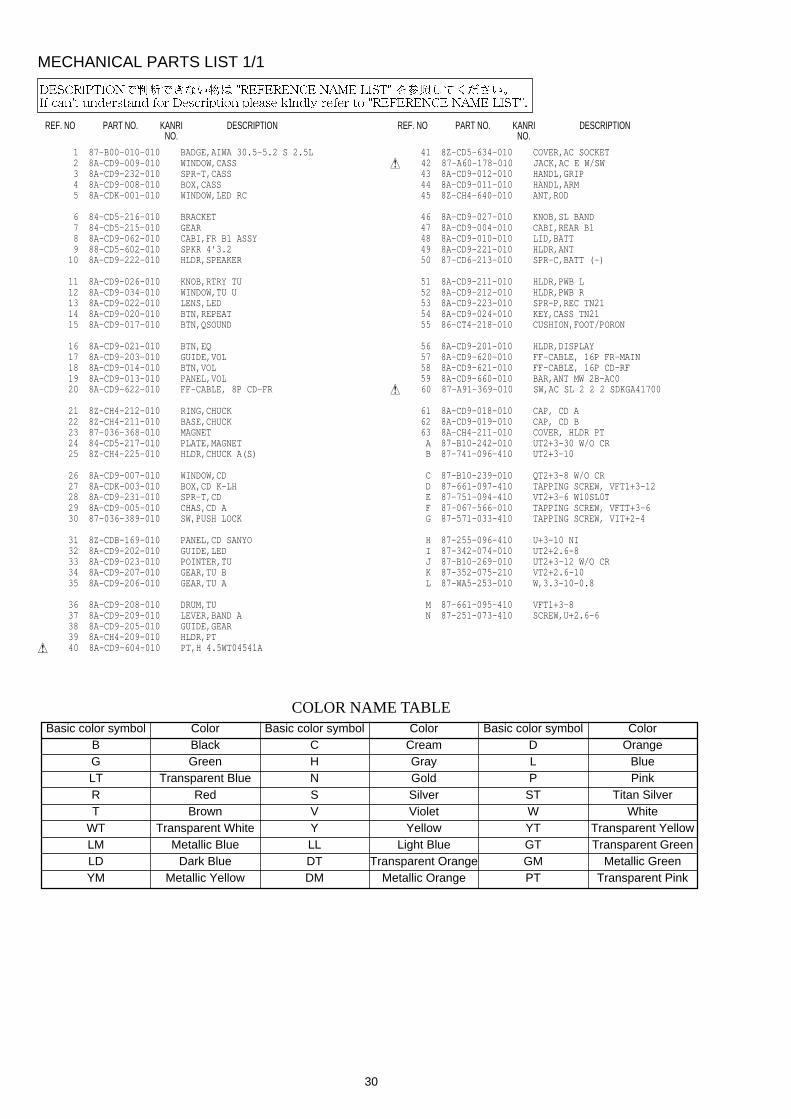
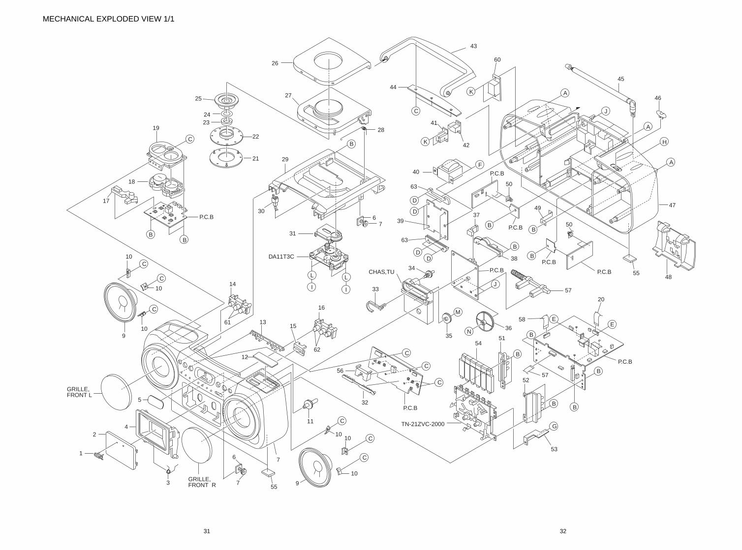
MECHANICAL PARTS LIST 1/1
1 87-B00-010-010 BADGE,AIWA 30.5-5.2 S 2.5L 2 8A-CD9-009-010 WINDOW,CASS 3 8A-CD9-232-010 SPR-T,CASS 4 8A-CD9-008-010 BOX,CASS 5 8A-CDK-001-010 WINDOW,LED RC
6 84-CD5-216-010 BRACKET 7 84-CD5-215-010 GEAR 8 8A-CD9-062-010 CABI,FR B1 ASSY 9 88-CD5-602-010 SPKR 4’3.2 10 8A-CD9-222-010 HLDR,SPEAKER
11 8A-CD9-026-010 KNOB,RTRY TU 12 8A-CD9-034-010 WINDOW,TU U 13 8A-CD9-022-010 LENS,LED 14 8A-CD9-020-010 BTN,REPEAT 15 8A-CD9-017-010 BTN,QSOUND
16 8A-CD9-021-010 BTN,EQ 17 8A-CD9-203-010 GUIDE,VOL 18 8A-CD9-014-010 BTN,VOL 19 8A-CD9-013-010 PANEL,VOL 20 8A-CD9-622-010 FF-CABLE, 8P CD-FR
21 8Z-CH4-212-010 RING,CHUCK 22 8Z-CH4-211-010 BASE,CHUCK 23 87-036-368-010 MAGNET 24 84-CD5-217-010 PLATE,MAGNET 25 8Z-CH4-225-010 HLDR,CHUCK A(S)
26 8A-CD9-007-010 WINDOW,CD 27 8A-CDK-003-010 BOX,CD K-LH 28 8A-CD9-231-010 SPR-T,CD 29 8A-CD9-005-010 CHAS,CD A 30 87-036-389-010 SW,PUSH LOCK
31 8Z-CDB-169-010 PANEL,CD SANYO 32 8A-CD9-202-010 GUIDE,LED 33 8A-CD9-023-010 POINTER,TU 34 8A-CD9-207-010 GEAR,TU B 35 8A-CD9-206-010 GEAR,TU A
36 8A-CD9-208-010 DRUM,TU 37 8A-CD9-209-010 LEVER,BAND A 38 8A-CD9-205-010 GUIDE,GEAR 39 8A-CH4-209-010 HLDR,PT! 40 8A-CD9-604-010 PT,H 4.5WT04541A
41 8Z-CD5-634-010 COVER,AC SOCKET! 42 87-A60-178-010 JACK,AC E W/SW 43 8A-CD9-012-010 HANDL,GRIP 44 8A-CD9-011-010 HANDL,ARM 45 8Z-CH4-640-010 ANT,ROD
46 8A-CD9-027-010 KNOB,SL BAND 47 8A-CD9-004-010 CABI,REAR B1 48 8A-CD9-010-010 LID,BATT 49 8A-CD9-221-010 HLDR,ANT 50 87-CD6-213-010 SPR-C,BATT (-)
51 8A-CD9-211-010 HLDR,PWB L 52 8A-CD9-212-010 HLDR,PWB R 53 8A-CD9-223-010 SPR-P,REC TN21 54 8A-CD9-024-010 KEY,CASS TN21 55 86-CT4-218-010 CUSHION,FOOT/PORON
56 8A-CD9-201-010 HLDR,DISPLAY 57 8A-CD9-620-010 FF-CABLE, 16P FR-MAIN 58 8A-CD9-621-010 FF-CABLE, 16P CD-RF 59 8A-CD9-660-010 BAR,ANT MW 2B-AC0! 60 87-A91-369-010 SW,AC SL 2 2 2 SDKGA41700
61 8A-CD9-018-010 CAP, CD A 62 8A-CD9-019-010 CAP, CD B 63 8A-CH4-211-010 COVER, HLDR PT A 87-B10-242-010 UT2+3-30 W/O CR B 87-741-096-410 UT2+3-10
C 87-B10-239-010 QT2+3-8 W/O CR D 87-661-097-410 TAPPING SCREW, VFT1+3-12 E 87-751-094-410 VT2+3-6 W10SL0T F 87-067-566-010 TAPPING SCREW, VFTT+3-6 G 87-571-033-410 TAPPING SCREW, VIT+2-4
H 87-255-096-410 U+3-10 NI I 87-342-074-010 UT2+2.6-8 J 87-B10-269-010 UT2+3-12 W/O CR K 87-352-075-210 VT2+2.6-10 L 87-WA5-253-010 W,3.3-10-0.8
M 87-661-095-410 VFT1+3-8 N 87-251-073-410 SCREW,U+2.6-6
COLOR NAME TABLEBasic color symbol Color Basic color symbol Color Basic color symbol Color
B Black C Cream D OrangeG Green H Gray L BlueLT Transparent Blue N Gold P PinkR Red S Silver ST Titan SilverT Brown V Violet W White
WT Transparent White Y Yellow YT Transparent YellowLM Metallic Blue LL Light Blue GT Transparent GreenLD Dark Blue DT Transparent Orange GM Metallic GreenYM Metallic Yellow DM Metallic Orange PT Transparent Pink
3231
MECHANICAL EXPLODED VIEW 1/1
24
5
3 7
6 7
9
10
1010
11
32
56
P.C.B
P.C.B
P.C.B
P.C.B
P.C.B
P.C.B
P.C.B
53
TN-21ZVC-2000
52
58
51
57
55
50
37
38
20
54
57
55
1
30
31
DA11T3C
67
I
DD
L
I
L
39
63
40
42
41
44
43
45
60
46
47
48
49
50
34
36
CHAS,TU
33
16
1513
14
61
6212
35
P.C.B
17
18
19
21
22
2324
25
26
27
28
29
10
10
910
GRILLE,FRONT R
GRILLE,FRONT L
63
D
E
H
A
J
A
A
E
B
B
C
C
C
C
C
C
N
M
B
BB
D
F
K
C
BC
BB
C
C
C
K
B
BB
G
J
B
3433
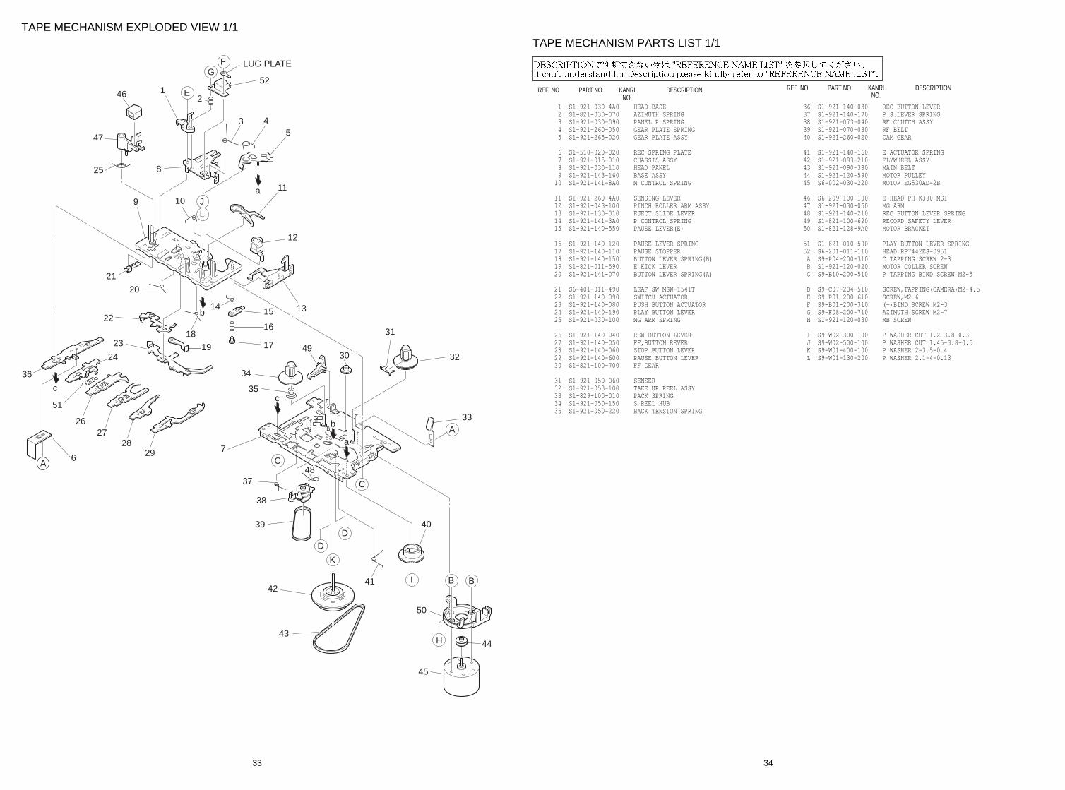
TAPE MECHANISM EXPLODED VIEW 1/1
b
c
a
a
b
c
JL
FG
E
LUG PLATE
52
2 1
3 45
11
10
8
9
46
47
25
21
20
18
19
22
23
24
2627
28296
14 15
16
17 49
34
35
36
51
13
C
C
30
7
37
38
48
B
50
45
44
K
I
DD
39 40
4142
43
B
H
A
32
31
33
12
A
REF. NO PART NO. KANRI DESCRIPTIONNO.
TAPE MECHANISM PARTS LIST 1/1
1 S1-921-030-4A0 HEAD BASE 2 S1-821-030-070 AZIMUTH SPRING 3 S1-921-030-090 PANEL P SPRING 4 S1-921-260-050 GEAR PLATE SPRING 5 S1-921-265-020 GEAR PLATE ASSY
6 S1-510-020-020 REC SPRING PLATE 7 S1-921-015-010 CHASSIS ASSY 8 S1-921-030-110 HEAD PANEL 9 S1-921-143-160 BASE ASSY 10 S1-921-141-8A0 M CONTROL SPRING
11 S1-921-260-4A0 SENSING LEVER 12 S1-921-043-100 PINCH ROLLER ARM ASSY 13 S1-921-130-010 EJECT SLIDE LEVER 14 S1-921-141-3A0 P CONTROL SPRING 15 S1-921-140-550 PAUSE LEVER(E)
16 S1-921-140-120 PAUSE LEVER SPRING 17 S1-921-140-110 PAUSE STOPPER 18 S1-921-140-150 BUTTON LEVER SPRING(B) 19 S1-821-011-590 E KICK LEVER 20 S1-921-141-070 BUTTON LEVER SPRING(A)
21 S6-401-011-490 LEAF SW MSW-1541T 22 S1-921-140-090 SWITCH ACTUATOR 23 S1-921-140-080 PUSH BUTTON ACTUATOR 24 S1-921-140-190 PLAY BUTTON LEVER 25 S1-921-030-100 MG ARM SPRING
26 S1-921-140-040 REW BUTTON LEVER 27 S1-921-140-050 FF,BUTTON REVER 28 S1-921-140-060 STOP BUTTON LEVER 29 S1-921-140-600 PAUSE BUTTON LEVER 30 S1-821-100-700 FF GEAR
31 S1-921-050-060 SENSER 32 S1-921-053-100 TAKE UP REEL ASSY 33 S1-829-100-010 PACK SPRING 34 S1-921-050-150 S REEL HUB 35 S1-921-050-220 BACK TENSION SPRING
REF. NO PART NO. KANRI DESCRIPTIONNO.
36 S1-921-140-030 REC BUTTON LEVER 37 S1-921-140-170 P.S.LEVER SPRING 38 S1-921-073-040 RF CLUTCH ASSY 39 S1-921-070-030 RF BELT 40 S1-921-260-020 CAM GEAR
41 S1-921-140-160 E ACTUATOR SPRING 42 S1-921-093-210 FLYWHEEL ASSY 43 S1-921-090-380 MAIN BELT 44 S1-921-120-590 MOTOR PULLEY 45 S6-002-030-220 MOTOR EG530AD-2B
46 S6-209-100-100 E HEAD PH-K380-MS1 47 S1-921-030-050 MG ARM 48 S1-921-140-210 REC BUTTON LEVER SPRING 49 S1-821-100-690 RECORD SAFETY LEVER 50 S1-821-128-9A0 MOTOR BRACKET
51 S1-821-010-500 PLAY BUTTON LEVER SPRING 52 S6-201-011-110 HEAD,RP7442ES-0951 A S9-P04-200-310 C TAPPING SCREW 2-3 B S1-921-120-020 MOTOR COLLER SCREW C S9-B10-200-510 P TAPPING BIND SCREW M2-5
D S9-C07-204-510 SCREW,TAPPING(CAMERA)M2-4.5 E S9-P01-200-610 SCREW,M2-6 F S9-B01-200-310 (+)BIND SCREW M2-3 G S9-F08-200-710 AZIMUTH SCREW M2-7 H S1-921-120-030 MB SCREW
I S9-W02-300-100 P WASHER CUT 1.2-3.8-0.3 J S9-W02-500-100 P WASHER CUT 1.45-3.8-0.5 K S9-W01-400-100 P WASHER 2-3.5-0.4 L S9-W01-130-200 P WASHER 2.1-4-0.13

35
REF. NO PART NO. KANRI DESCRIPTIONNO.
CD MECHANISM EXPLODED VIEW 1/1
CD MECHANISM PARTS LIST 1/1
1 S2-121-A28-400 COVER GEAR 2 S2-511-A21-000 GEAR MIDDLE 3 S2-511-A21-100 GEAR,DRIVE A S1-PN2-03R-OSE SCR PAN PCS 2-3 B 87-261-073-410 SCR S-TPG FLT 2.6-6
ALL M8-ZZK-E90-070 DA11T3C
B
B
A
A
SHAFT,SLIDE
1
2
3
MOTOR C,BSPINDLEMOTOR(M1)
CHASSIS
SF-P101NR

2–11, IKENOHATA 1–CHOME, TAITO-KU, TOKYO 110, JAPAN TEL:03 (3827) 3111
920074 Printed in Singapore