Embed Size (px)
Citation preview
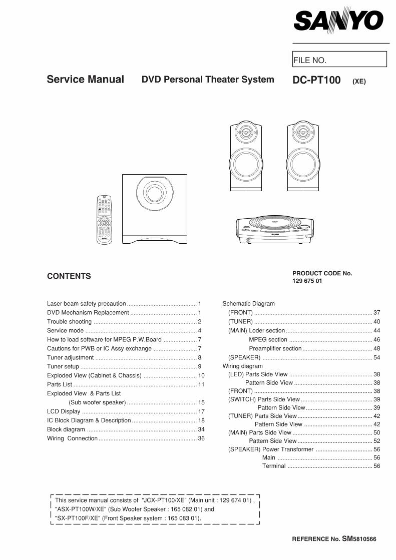
FILE NO.
Service Manual
CONTENTS
DVD Personal Theater System DC-PT100 (XE)
PRODUCT CODE No.129 675 01
REFERENCE No. SM5810566
Laser beam safety precaution .......................................... 1
DVD Mechanism Replacement ........................................ 1
Trouble shooting .............................................................. 2
Service mode ................................................................... 4
How to load software for MPEG P.W.Board .................... 7
Cautions for PWB or IC Assy exchange .......................... 7
Tuner adjustment ............................................................. 8
Tuner setup ...................................................................... 9
Exploded View (Cabinet & Chassis) ................................ 10
Parts List .......................................................................... 11
Exploded View & Parts List
(Sub woofer speaker) .......................................... 15
LCD Display ..................................................................... 17
IC Block Diagram & Description ....................................... 18
Block diagram .................................................................. 34
Wiring Connection ........................................................... 36
Schematic Diagram
(FRONT) ....................................................................... 37
(TUNER) ....................................................................... 40
(MAIN) Loder section .................................................... 44
MPEG section .................................................. 46
Preamplifier section .......................................... 48
(SPEAKER) .................................................................. 54Wiring diagram
(LED) Parts Side View .................................................. 38Pattern Side View ............................................... 38
(FRONT) ....................................................................... 38(SWITCH) Parts Side View ........................................... 39
Pattern Side View........................................ 39(TUNER) Parts Side View............................................. 42
Pattern Side View ......................................... 42(MAIN) Parts Side View ................................................ 50
Pattern Side View ............................................. 52(SPEAKER) Power Transformer .................................. 56
Main ......................................................... 56Terminal ................................................... 56
This service manual consists of "JCX-PT100/XE" (Main unit : 129 674 01) ,
"ASX-PT100W/XE" (Sub Woofer Speaker : 165 082 01) and
"SX-PT100F/XE" (Front Speaker system : 165 083 01).
VOLUME
SOUND
FUNCTION SURROUNDTUNING
PRESET
PHONES
REMOTE CONTROLLER RB-PT100RDS
- 1 -
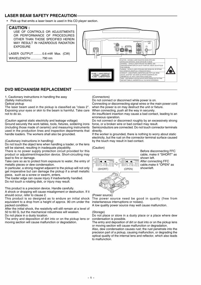
LASER BEAM SAFETY PRECAUTION• Pick-up that emits a laser beam is used in this CD player section.
CAUTION :USE OF CONTROLS OR ADJUSTMENTSOR PERFORMANCE OF PROCEDURESOTHER THAN THOSE SPECIFIED HEREINMAY RESULT IN HAZARDOUS RADIATIONEXPOSURE
LASER OUTPUT.......... 0.6 mW Max. (CW)
WAVELENGTH ............. 790 nm
S-VIDEOOUT
VIDEOOUT
AUDIOOUT
CONTROL
TO SUBWOOFER
OPT.DIGITALOUT
CAUTION – INVISIBLE LASER RADIATION WHEN OPEN ANDINTERLOCKS DEFEATED. AVOID EXPOSURE TO BEAM.ADVARSEL – USYNLIG LASER STRÅLING VED ÅBNING, NÅRSIKKERHEDSAFBRYDERE ER UDE AF FUNKTION, UNDGÅ UDS ÆTTELSEFOR STRÅLING.VARNING – OSYNLIG LASER STRÅLNING NÄR DENNA DEL ÄR ÖPPNADOCH SPÄRR ÄR URKOPPLAD. STRÅLEN ÄR FARLIG.VORSICHT – UNSICHTBARE LASERSTRAHLUNG TRITT AUS, WENNDECKEL GEÖFFNET UND WENN SICHERHEITSVERRIEGELUNGÜBERBRÜCKT IST. NICHT, DEM STRAHL AUSSETZEN.VARO – AVATTAESSA JA SUOJALUKITUS OHITETTAESSA OLET ALTTIINANÄKYMÄTTÖMÄLLE LASERSÄTEILYLLE. ÄLÄ KATSO SÄTEESEEN.
1. Cautionary instructions in handling the assy(Safety instructions)Optical pickupThe laser beam used in the pickup is classified as "class 2".Exposing your eyes or skin to the beam is harmful. Take carenot to do so.
(Caution against static electricity and leakage voltage)Ground securely the work tables, tools, fixtures, soldering irons(including those made of ceramic) and measuring instrumentsused in the production lines and inspection departments thathandle loaders. The workers shall also be grounded.
(Cautionary instructions in handling)Do not touch the object lens when handling a loader, or the lenswill be stained, resulting in inadequate playability.There is no power supply protection circuit provided for thisproduct or adjustment/inspection device. Short-circuiting maylead to fire or damage.Take care so as to protect from exposure to water, the entry ofmetallic pieces or dew condensation.In particular, a strong magnet adjacent to the pickup will not onlyget inoperative but can damage the pickup if a small metallicpiece, such as a screw or swarm, enters.The loader edge can cause injury if inadvertently handled.Do not touch a rotating disk, or injury may result.
This product is a precision device. Handle carefully.A shock or dropping will cause misalignment or destruction. If itshould occur, refer to clause 2.This product is so designed as to endure an initial shockequivalent to a drop from a height of approx. 90 cm under thepacked condition.After the initial shock, the resistivity will still remain at a level of50 to 60 G, but the mechanical robustness will weaken.Do not place in a dusty location.The entry and deposition of dirt into or on the pickup lens ormoving section will cause malfunction or degradation.
DVD MECHANISM REPLACEMENT
(Connectors)Do not connect or disconnect while power is on.Connecting or disconnecting signal wires or the main power cordwhen the power is on may destruct the unit or fixture.When connecting, push all the way in securely.An insufficient insertion may cause a bad contact, leading to anerroneous operation.Do not connect or disconnect roughly by an excessively strongforce, or a broken wire or bad contact may result.Semiconductors are connected. Do not touch connector terminalsdirectly.If the worker is grounded, there is nothing to worry about staticelectricity, but the rust on the connector terminal surface causedby the touch may result in bad contact.
(Caution) Before disconnecting FFC cable, make it "SHORT" as shown left. After connecting FFC cable,make it "OPEN" as shownleft.
(Power source)The power source need be good in quality (free frominstantaneous interruptions or noises).A low quality power source may well cause malfunction.
(Storage)Do not place or store in a dusty place or a place where dewcondensation is possible.The entry and deposition of dirt or dust into or on the pickup lensor moving section will cause malfunction or degradation.Also, dew condensation causes rust; the rust penetrate into theprecision part of a pickup, causing malfunction, or degrading theoptical quality of the internal lens and reflector, which also leadsto malfunction.
(OPEN)(SHORT)

- 6 -
SERVICE MODE
4. Setting REGION code4.1 While a highlighted indicator is displayed on the right side
of the Region denotation, push ENT, -> and <- each button
on the remote controller. With each push the indicator will
advance as shown below.
1 <-> 2 <-> 3 <-> 4 <-> 5 <-> 64.2 Specify the number of the model in accordance with the
Market/Region Setup Table above.
4.3 Once the desired number is displayed, push p button to
move the highlighted indicator to Exit area.
5. Saving settings5.1 Make sure that the Market and Region settings are properly
set.
(If any of the settings are incorrect, you can make a change
by moving the indicator using o button, and following
procedures 3 and 4 above. )
5.2 After ensuring that the settings are all correct, push ENT
button while the indicator is on Exit area. The settings are
now saved.
6. Finishing settings6.1 After a few seconds, the Internal Setup screen disappears,
and then the Service Mode screen is displayed again for
three seconds as shown on the right.
You should check the settings.
Region 1 M a r k e t
W MBackendVersion S21225A1LoaderVersion 16 Z08 W03
Value
Service Mode Sceen after settings
Backend version S 21225 A 0
Brand (S : SANYO , F : FISHER)
Version ( 2 0 0 2 . 12 . 25)
Sub Version (A,B,......Z)
Region ( 0 : Region undefined
1 ~ 6 : Region defined )
Loader Version (16 Z08 W03)
6.2 Power OFF.
00 1
1
Internal SetupM a r k e tRegion
Exit
00-WM 01-SFC 02-UK 03-XES1805-SS 06-PA 07-AU 08-CN 09-JP
04-
Internal Setup00M a r k e t1Region
Exit
00-WM 01-SFC 02-UK 03-XES1805-SS 06-PA 07-AU 08-CN 09-JP
04-

- 7 -
SERVICE MODE
D. IMPORTANT NOTE1. Once the "Market/Region" settings are written into EEPROM (IC801) on the DVD substrate, they cannot be reset.
(However, updating the system using CD-R enables you to make new settings.)
2. While the Internal Setup screen is displayed, pushing the Power button enables you to terminate the operations without
making any settings.
HOW TO LOAD SOFTWARE FOR MPEG P.W.BOARD
1. Power on, then open tray.
2. It take on CD-ROM for UPDATE software to the tray, and tray close.
3. For the time being, tray open and FL display remain "UP DATING".
4. When software loading finished, "GOOD-BY" on a FL display disappears.
5. Next, set up market code and region code by "SERVICE MODE"
CD-ROM part code is "0PRADC9674--A".
CAUTIONS FOR PWB or IC ASSY EXCHANGE
After an MAIN board(614 328 1603) or IC ASSY(410 489 6705) exchange should carry out loading of the software by thenewest CD-R, and should check operation.
- 8 -
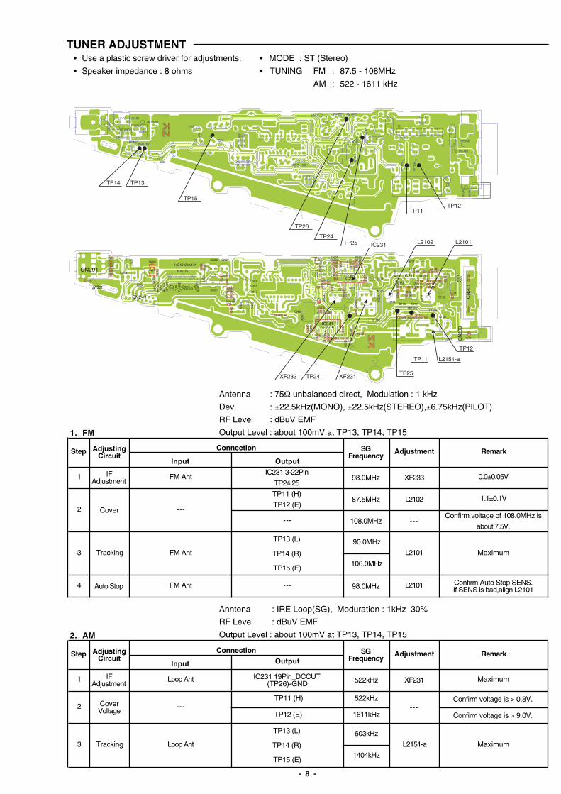
TUNER ADJUSTMENT
Antenna : 75Ω unbalanced direct, Modulation : 1 kHz
Dev. : ±22.5kHz(MONO), ±22.5kHz(STEREO),±6.75kHz(PILOT)
RF Level : dBuV EMF
Output Level : about 100mV at TP13, TP14, TP15
Anntena : IRE Loop(SG), Moduration : 1kHz 30%
RF Level : dBuV EMF
Output Level : about 100mV at TP13, TP14, TP15
• Use a plastic screw driver for adjustments. • MODE : ST (Stereo)
• Speaker impedance : 8 ohms • TUNING FM : 87.5 - 108MHz
AM : 522 - 1611 kHz
1AD4B10D2011A
24 20
13
12101
242013
12 10 1
NC(G
ND)
DIDO
TU.G
ND
5.6V
HP_S
W
HP-R
HP-L
CLK
CETU-L
TU-R
+12V
HP_M
UT
HP.G
ND
LC72121M
LA1844 TA8176S
SH20
1
94V-0 F01
TP11(H)TP12(E)
0V ADJ
R2303
CN291
X245
1
D2301L250
3
R2101
L2103
C2301
C2122
XF23
1
CN
203
CN
201
CN241
IC211
XF23
3
B2101
D2102 D2101
XF222
XF22
1
L210
1
L2102
C2311
C231
7
R2113
C2465
C2327
L2903
C2307
C230
3
R2311
C2328
R2301
R245
5
D245
2
C2991
L245
1
C245
1
L2151
JW201
XF21
1
L2901
L290
2
CAN
Q2902
C21
21
R2111
IC241
IC231C2123C2101R
2106 C2103
C2102
C2104C2126
R21
04
C2105
R21
02R
2103
C2112C2109C2108
C210
6
R2112
C210
7
C2111
C2151 C2152R2151
Q2901
C21
31C
2130
R2303
C2312C23
10
R23
09
R2308
C23
20C
2319
C230
9C2
316
R230
7
R23
02
C23
04
C2302C2321
C2306R23
06
C23
22
C2452
C23
30
C24
53C
2454
C24
62
C2464C24
63
C24
61
C2117 R2114C24
55R
2452
C24
57
R2453R
2304
R2305
D2451
Q2451
R2465R2454
R24
59
R24
58
R27
12 R2711
R28
11R
2812
SG29
3SG
292
SG
291
R29
02R
2901
C29
02C
2901
C29
03
R24
63
R24
64
R2462R2461
C29
92
C2314C2308
C23
15R2153
C2113
C2305
C2456
CAN
C23
18
C2904
D2104
D2151
12
1
0V ADJ
RDS IO0
AM DETFM DETGND
GND
DO
DITU-LTU-RHP-MUT
HP-SW1
HP-S
W2
HP.GND2
HP-R2 HP-R1
HP-L1
HP-L2HP.GND1
+12V
CE CLK
5.6V
0V-T
P1
0V-T
P2
TP11
(H)
TP12
(E)
AM-A
NT
AM.G
ND
FM-ANT
FM.GND
L2151-aTP11
TP12
L2102 L2101
TP25XF231XF233 TP24
TP24
TP26
TP15
TP13TP14
TP25
TP11TP12
IC231
Input Output
IC231 3-22Pin
TP24,25
TP11 (H)
TP12 (E)
Confirm voltage of 108.0MHz is
about 7.5V.
90.0MHz
106.0MHz
4 Auto Stop FM Ant --- 98.0MHz L2101 Confirm Auto Stop SENS.If SENS is bad,align L2101
Input Output
1 IFAdjustment
Loop Ant IC231 19Pin_DCCUT(TP26)-GND 522kHz XF231 Maximum
603kHz
1404kHz
---
SGFrequency
98.0MHz XF233
Adjustment
0.0±0.05V
L2102 1.1±0.1V
FM Ant
87.5MHz
RemarkSGFrequency
2 CoverVoltage
--- TP11 (H)
IFAdjustment
1
Adjustment
---
1. FM
Step AdjustingCircuit
Connection
--- 108.0MHz
Tracking3
2 Cover
2. AM
Step AdjustingCircuit
Connection
3 Tracking
522kHz---
TP13 (L)
TP14 (R)
TP15 (E)
Loop Ant L2151-a
TP12 (E) 1611kHz
Maximum
TP13 (L)
TP14 (R)
TP15 (E)
FM Ant L2101 Maximum
Confirm voltage is > 0.8V.
Confirm voltage is > 9.0V.
Remark
- 9 -
TUNER SETUP
1. DESTINATION SETTING1.1 Press "POWER" button to turn on the power.1.2 Change to "AUX Function" or "DVD/CD Function".
1.3 Press "SOUND" button and "POWER" button on the main unit at the same time.
1.4 Release "SOUND" button and "POWER" button at the same time, then within 1 second, press
"TUNING(REV)" button on the main unit.1.5 The present tuner destination appears on the LCD.
(See Fig.1) (It appears for 3 seconds on the LCD)
2. DESTINATION CHANGING2.1 While the tuner destination appears on the LCD for 3
seconds, press "STOP" button. (Fig.1)
LCD display will not disappear even after 3 seconds.2.2 Tuner destination can be changed at this stage.(Fig.2)
2.3 Whenever the "+TUNING(FWD)" button on the main unit is pressed, the tuner destination will be changed.
3. RDS FUNCTION and KARAOKE FUNCTION
SETTING3.1 When the tuner destination selects, RDS function can
be selected by pressing "PRESET(PREV)" button on the main unit.
3.2 When the tuner destination selects, KARAOKE function can be selected by pressing
"PRESET(NEXT)" button on the main unit.
LCD DISPLAY
U S
U S
U S
E U 2 R
S S K
S S K
J P 2
N X J P
N X J P T V
E U 3 R
E U 2 R
S S
E U 2
S S J P 2 +
(Fig.1)
(Fig.2)
(Fig.3)
RDS function YES
KARAOKE function YES
KARAOKE function NO
RDS function NO
KARAOKE function"K" = KARAOKE function "YES"
RDS function"R" = RDS function "YES"
Destination
3.3 After "Tuner Destination", "RDS function" and
"KARAOKE function" is selected, press "POWER" button on the main unit 3 times. (POWER OFF POWER ON POWER OFF) Unplug and plug in the AC cord after that. And check on the accuracy of the each setting.
Here is the end. All settings are determined.
* NOTES1. Tuner destination display can be changed while
tuner functions.2. Tuner destination setting can be initialized by RAM
CLEAR (Initialization).
*TUNER initial setting Destination "EU2" and "EU3" : RDS function "YES" Destination "SS" : KARAOKE function "YES"
2.4 After the tuner destination is selected, press "POWER" button on the main unit 3 times. (POWER OFF POWER ON POWER OFF) Unplug and plug in the AC cord after that. And check on the accuracy of the each setting.
* This model setting is "EU2 R".
* This model setting is "EU2 R".
* This model has no KARAOKE function.
*
*
- 10 -
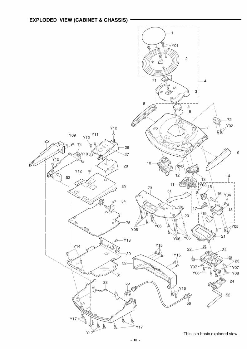
EXPLODED VIEW (CABINET & CHASSIS)
This is a basic exploded view.
1
2
3
4
56
7
8
9
10
11
1213
15
16
17 18
21
22
23
24
20
34
71
Y01
Y02
Y03
Y04
Y05Y06
Y06
Y09 Y11
Y12
Y12
Y10
Y12
Y12
Y13Y15
Y15
Y16
Y17
Y17
Y17
Y14
Y06 Y06
Y07 Y07Y08Y08
72
19
5173
14
74
53
52
26
27
28
25
29
54
75
30
31
32
5533
56

- 11 -
PARTS LIST
CAUTION : Regular type resistors and capacitors are not listed. To know those values, refer to the schematic diagram.Regular type resistors are less than 1/4 W carbon type and 0 ohm chip resistors.Regular type capacitors are less than 50 V and less than 1000 µF type of Ceramic type and Electrical type.
N.S.P : Not available as service parts.
PRODUCT SAFETY NOTICEEACH PRECAUTION IN THIS MANUAL SHOULD BE FOLLOWED DURING SERVICING. COMPONENTS IDENTIFIED WITH THEIEC SYMBOL !!! IN THE PARTS LIST AND THE SCHEMATIC DIAGRAM DESIGNATED COMPONENTS IN WHICH SAFETY ANDPERFORMANCE CAN BE OF SPECIAL SIGNIFICANCE. WHEN REPLACING A COMPONENT IDENTIFIED BY !!! , USE ONLY THEREPLACEMENT PARTS DESIGNATED, OR PARTS WITH THE SAME RATINGS OF RESISTANCE, WATTAGE OR VOLTAGE THATARE DESIGNATED IN THE PARTS LIST IN THIS MANUAL. LEAKAGE-CURRENT OR RESISTANCE MEASUREMENTS MUST BEMADE TO DETERMINE THAT EXPOSED PARTS ARE ACCEPTABLY INSULATED FROM THE SUPPLY CIRCUIT BEFORERETURNING THE PRODUCT TO THE CUSTOMER.
REF.NO. PART NO. DESCRIPTIONPACKING & ACCESSORIESREF.NO. PART NO. DESCRIPTION
614 328 5175 CARTON CASE614 327 1673 CUSHION,L614 327 1680 CUSHION,R614 328 5205 INSTRUCTION MANUAL614 329 5419 INSTRUCTION MANUAL,GREEK645 041 1533 POLY SHEET-0750X0500*NC,SET645 045 3540 POLY SHEET-1100X0600*NC,
SPEAKER614 229 4635 FM ANTENNA
or 614 308 5515 FM ANTENNA645 063 4031 LOOP,AM LOOP ANTENNA645 064 7819 REMOCON,RB-PT100RDS645 063 5052 CABLE,AUDIO
or 645 064 7994 CABLE,AUDIO614 327 5664 ASSY,WIRE645 066 9330 CABLE,VIDEO614 329 0995 ASSY,BOX,SPEAKER,FRONT
CABINET & CHASSISREF.NO. PART NO. DESCRIPTION1 614 329 6188 DEC,SHEET,DVD2 614 327 1468 DEC,WINDOW DVD3 614 327 1574 LID,DVD4 614 328 5069 ASSY,LID DVDor 614 329 6157 ASSY,LID,DVD5 614 327 1567 KNOB,VR,VOL.6 614 328 4475 DEC,SHEET,JOG,
CAB.TOP-KNOB,VR7 614 327 1338 ASSY,CABINET,TOP8 614 327 1598 PANEL,SIDE,L9 614 327 1604 PANEL,SIDE,R10 614 327 2595 ASSY,BUTTON,L11 614 327 2601 ASSY,BUTTON,R12 614 327 1499 DEC,WINDOW,IR13 614 327 1475 DEC,RING,VOL.14 614 327 2625 ASSY,MOUNTING,GEAR15 614 327 1536 GEAR,HERI-SPUR16 614 327 1406 BELT,SQUARE17 614 327 1543 GEAR,WORM-PULLEY18 614 327 1581 MOUNTING,GEAR19 645 032 5861 MOTOR,DC 0.2W20 614 327 5541 SPRING,COMP,PWB,TOP21 614 327 1451 COVER,MECHA,DVD22 614 301 1552 SPACER,MECHA,DVD,MECHA23 614 310 3899 SPACER,MECHA,DVD MECHA24 614 327 1529 FIXER,PICK,FFC,DVD MECHA25 614 327 1642 SHIELD,TU,L,TU PWB26 614 327 4681 SHIELD,PWB,POWER,DVD27 614 328 2150 SPACER,SHIELD28 614 327 4674 SPACER,COVER,
DVD(POWER) PWB29 614 327 1628 SHIELD,DVD,TOP,DVD PWB30 614 327 1635 SHIELD,DVD,BOTTOM,DVD PWB31 614 328 4109 SPACER,PWB,BOTTOM,SHIELD32 614 327 1437 CABINET,REAR
FIXING PARTSREF.NO. PART NO. DESCRIPTIONY01 411 021 6405 SCR S-TPG BIN 3X8,LID+WINDOWY02 411 165 3803 SCR S-TPG BIN 2.3X10,SW PWBY03 411 187 1801 SCR S-TPG PAN+FLG 2X10,GEARY04 411 044 7502 SCR PAN+SW 2X5,MOTORY05 411 165 3803 SCR S-TPG BIN 2.3X10,ASSY,GEARY06 411 165 3803 SCR S-TPG BIN 2.3X10,TOP PWBY07 411 092 0906 WASHER Z 2.6X10X0.5,DVD MECHAY08 411 021 1806 SCR S-TPG BIN 2.6X10,DVD MECHAY09 411 021 4104 SCR S-TPG BIN 3X12,
TU PWB+SHIELDY10 411 021 6405 SCR S-TPG BIN 3X8,
TU PWB+SHIELDY11 411 021 6405 SCR S-TPG BIN 3X8,
SHIELD,PWR+BOTTOMY12 411 021 6405 SCR S-TPG BIN 3X8,
DVD PWB-SHIELDY13 411 021 4104 SCR S-TPG BIN 3X12,
DVD PWB-SHIELDY14 411 021 6405 SCR S-TPG BIN 3X8,
SHIELD+BOTTOMY15 411 021 4104 SCR S-TPG BIN 3X12,
REAR+SOCKETY16 411 021 4005 SCR S-TPG BIN 3X12,
BOTTOM+REARY17 411 021 4005 SCR S-TPG BIN 3X12,
TOP+BOTTOM
ELECTRICAL PARTSREF.NO. PART NO. DESCRIPTION51 645 061 4422 FLEXIBLE FLAT CABLE,
MAIN-FRONT(28P)52 645 061 4637 FLEXIBLE FLAT CABLE,
MAIN-PICK(24P)53 645 061 4415 FLEXIBLE FLAT CABLE,
MAIN-TUNER(15P)54 423 028 8207 FUSE 250V 1A,250V 1A55 645 051 0649 CORE,FERRITE,FOR AC CORDor 645 031 7637 CORE,FERRITE,FOR AC CORD56 645 061 4965 CORD,POWER-1.76MK,FOR XE
33 614 327 2618 ASSY,CABINET,BOTTOM34 614 327 4438 500AVST3 SE BA,
MECHANISM ASSY
- 12 -
PARTS LISTREF.NO. PART NO. DESCRIPTION
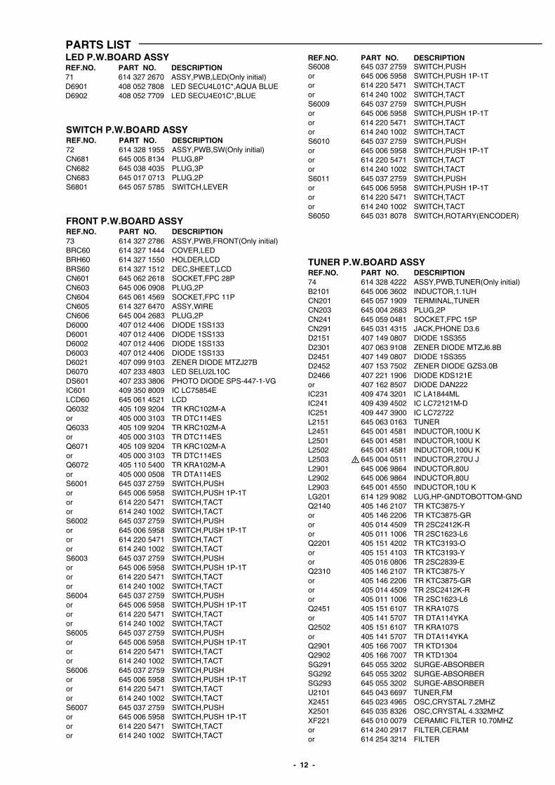
SWITCH P.W.BOARD ASSYREF.NO. PART NO. DESCRIPTION72 614 328 1955 ASSY,PWB,SW(Only initial)CN681 645 005 8134 PLUG,8PCN682 645 038 4035 PLUG,3PCN683 645 017 0713 PLUG,2PS6801 645 057 5785 SWITCH,LEVER
FRONT P.W.BOARD ASSYREF.NO. PART NO. DESCRIPTION73 614 327 2786 ASSY,PWB,FRONT(Only initial)BRC60 614 327 1444 COVER,LEDBRH60 614 327 1550 HOLDER,LCDBRS60 614 327 1512 DEC,SHEET,LCDCN601 645 062 2618 SOCKET,FPC 28PCN603 645 006 0908 PLUG,2PCN604 645 061 4569 SOCKET,FPC 11PCN605 614 327 6470 ASSY,WIRECN606 645 004 2683 PLUG,2PD6000 407 012 4406 DIODE 1SS133D6001 407 012 4406 DIODE 1SS133D6002 407 012 4406 DIODE 1SS133D6003 407 012 4406 DIODE 1SS133D6021 407 099 9103 ZENER DIODE MTZJ27BD6070 407 233 4803 LED SELU2L10CDS601 407 233 3806 PHOTO DIODE SPS-447-1-VGIC601 409 350 8009 IC LC75854ELCD60 645 061 4521 LCDQ6032 405 109 9204 TR KRC102M-Aor 405 000 3103 TR DTC114ESQ6033 405 109 9204 TR KRC102M-Aor 405 000 3103 TR DTC114ESQ6071 405 109 9204 TR KRC102M-Aor 405 000 3103 TR DTC114ESQ6072 405 110 5400 TR KRA102M-Aor 405 000 0508 TR DTA114ESS6001 645 037 2759 SWITCH,PUSHor 645 006 5958 SWITCH,PUSH 1P-1Tor 614 220 5471 SWITCH,TACTor 614 240 1002 SWITCH,TACTS6002 645 037 2759 SWITCH,PUSHor 645 006 5958 SWITCH,PUSH 1P-1Tor 614 220 5471 SWITCH,TACTor 614 240 1002 SWITCH,TACTS6003 645 037 2759 SWITCH,PUSHor 645 006 5958 SWITCH,PUSH 1P-1Tor 614 220 5471 SWITCH,TACTor 614 240 1002 SWITCH,TACTS6004 645 037 2759 SWITCH,PUSHor 645 006 5958 SWITCH,PUSH 1P-1Tor 614 220 5471 SWITCH,TACTor 614 240 1002 SWITCH,TACTS6005 645 037 2759 SWITCH,PUSHor 645 006 5958 SWITCH,PUSH 1P-1Tor 614 220 5471 SWITCH,TACTor 614 240 1002 SWITCH,TACTS6006 645 037 2759 SWITCH,PUSHor 645 006 5958 SWITCH,PUSH 1P-1Tor 614 220 5471 SWITCH,TACTor 614 240 1002 SWITCH,TACTS6007 645 037 2759 SWITCH,PUSHor 645 006 5958 SWITCH,PUSH 1P-1Tor 614 220 5471 SWITCH,TACTor 614 240 1002 SWITCH,TACT
TUNER P.W.BOARD ASSYREF.NO. PART NO. DESCRIPTION74 614 328 4222 ASSY,PWB,TUNER(Only initial)B2101 645 006 3602 INDUCTOR,1.1UHCN201 645 057 1909 TERMINAL,TUNERCN203 645 004 2683 PLUG,2PCN241 645 059 0481 SOCKET,FPC 15PCN291 645 031 4315 JACK,PHONE D3.6D2151 407 149 0807 DIODE 1SS355D2301 407 063 9108 ZENER DIODE MTZJ6.8BD2451 407 149 0807 DIODE 1SS355D2452 407 153 7502 ZENER DIODE GZS3.0BD2466 407 221 1906 DIODE KDS121Eor 407 162 8507 DIODE DAN222IC231 409 474 3201 IC LA1844MLIC241 409 439 4502 IC LC72121M-DIC251 409 447 3900 IC LC72722L2151 645 063 0163 TUNERL2451 645 001 4581 INDUCTOR,100U KL2501 645 001 4581 INDUCTOR,100U KL2502 645 001 4581 INDUCTOR,100U KL2503 645 004 0511 INDUCTOR,270U JL2901 645 006 9864 INDUCTOR,80UL2902 645 006 9864 INDUCTOR,80UL2903 645 001 4550 INDUCTOR,10U KLG201 614 129 9082 LUG,HP-GNDTOBOTTOM-GNDQ2140 405 146 2107 TR KTC3875-Yor 405 146 2206 TR KTC3875-GRor 405 014 4509 TR 2SC2412K-Ror 405 011 1006 TR 2SC1623-L6Q2201 405 151 4202 TR KTC3193-Oor 405 151 4103 TR KTC3193-Yor 405 016 0806 TR 2SC2839-EQ2310 405 146 2107 TR KTC3875-Yor 405 146 2206 TR KTC3875-GRor 405 014 4509 TR 2SC2412K-Ror 405 011 1006 TR 2SC1623-L6Q2451 405 151 6107 TR KRA107Sor 405 141 5707 TR DTA114YKAQ2502 405 151 6107 TR KRA107Sor 405 141 5707 TR DTA114YKAQ2901 405 166 7007 TR KTD1304Q2902 405 166 7007 TR KTD1304SG291 645 055 3202 SURGE-ABSORBERSG292 645 055 3202 SURGE-ABSORBERSG293 645 055 3202 SURGE-ABSORBERU2101 645 043 6697 TUNER,FMX2451 645 023 4965 OSC,CRYSTAL 7.2MHZX2501 645 035 8326 OSC,CRYSTAL 4.332MHZXF221 645 010 0079 CERAMIC FILTER 10.70MHZor 614 240 2917 FILTER,CERAMor 614 254 3214 FILTER
S6008 645 037 2759 SWITCH,PUSHor 645 006 5958 SWITCH,PUSH 1P-1Tor 614 220 5471 SWITCH,TACTor 614 240 1002 SWITCH,TACTS6009 645 037 2759 SWITCH,PUSHor 645 006 5958 SWITCH,PUSH 1P-1Tor 614 220 5471 SWITCH,TACTor 614 240 1002 SWITCH,TACTS6010 645 037 2759 SWITCH,PUSHor 645 006 5958 SWITCH,PUSH 1P-1Tor 614 220 5471 SWITCH,TACTor 614 240 1002 SWITCH,TACTS6011 645 037 2759 SWITCH,PUSHor 645 006 5958 SWITCH,PUSH 1P-1Tor 614 220 5471 SWITCH,TACTor 614 240 1002 SWITCH,TACTS6050 645 031 8078 SWITCH,ROTARY(ENCODER)
LED P.W.BOARD ASSYREF.NO. PART NO. DESCRIPTION71 614 327 2670 ASSY,PWB,LED(Only initial)D6901 408 052 7808 LED SECU4L01C*,AQUA BLUED6902 408 052 7709 LED SECU4E01C*,BLUE
- 13 -
PARTS LISTREF.NO. PART NO. DESCRIPTION
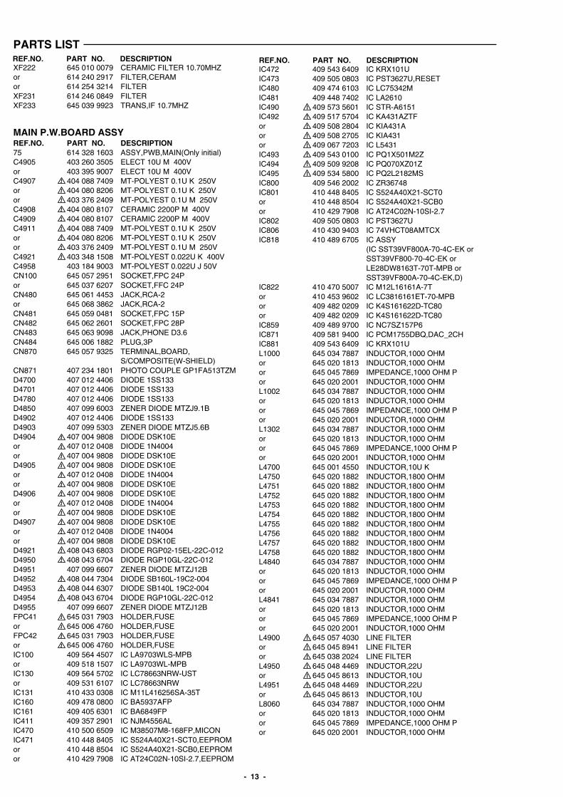
MAIN P.W.BOARD ASSYREF.NO. PART NO. DESCRIPTION75 614 328 1603 ASSY,PWB,MAIN(Only initial)C4905 403 260 3505 ELECT 10U M 400Vor 403 395 9007 ELECT 10U M 400VC4907 404 088 7409 MT-POLYEST 0.1U K 250Vor 404 080 8206 MT-POLYEST 0.1U K 250Vor 403 376 2409 MT-POLYEST 0.1U M 250VC4908 404 080 8107 CERAMIC 2200P M 400VC4909 404 080 8107 CERAMIC 2200P M 400VC4911 404 088 7409 MT-POLYEST 0.1U K 250Vor 404 080 8206 MT-POLYEST 0.1U K 250Vor 403 376 2409 MT-POLYEST 0.1U M 250VC4921 403 348 1508 MT-POLYEST 0.022U K 400VC4958 403 184 9003 MT-POLYEST 0.022U J 50VCN100 645 057 2951 SOCKET,FPC 24Por 645 037 6207 SOCKET,FFC 24PCN480 645 061 4453 JACK,RCA-2or 645 068 3862 JACK,RCA-2CN481 645 059 0481 SOCKET,FPC 15PCN482 645 062 2601 SOCKET,FPC 28PCN483 645 063 9098 JACK,PHONE D3.6CN484 645 006 1882 PLUG,3PCN870 645 057 9325 TERMINAL,BOARD,
S/COMPOSITE(W-SHIELD)CN871 407 234 1801 PHOTO COUPLE GP1FA513TZMD4700 407 012 4406 DIODE 1SS133D4701 407 012 4406 DIODE 1SS133D4780 407 012 4406 DIODE 1SS133D4850 407 099 6003 ZENER DIODE MTZJ9.1BD4902 407 012 4406 DIODE 1SS133D4903 407 099 5303 ZENER DIODE MTZJ5.6BD4904 407 004 9808 DIODE DSK10Eor 407 012 0408 DIODE 1N4004or 407 004 9808 DIODE DSK10ED4905 407 004 9808 DIODE DSK10Eor 407 012 0408 DIODE 1N4004or 407 004 9808 DIODE DSK10ED4906 407 004 9808 DIODE DSK10Eor 407 012 0408 DIODE 1N4004or 407 004 9808 DIODE DSK10ED4907 407 004 9808 DIODE DSK10Eor 407 012 0408 DIODE 1N4004or 407 004 9808 DIODE DSK10ED4921 408 043 6803 DIODE RGP02-15EL-22C-012D4950 408 043 6704 DIODE RGP10GL-22C-012D4951 407 099 6607 ZENER DIODE MTZJ12BD4952 408 044 7304 DIODE SB160L-19C2-004D4953 408 044 6307 DIODE SB140L 19C2-004D4954 408 043 6704 DIODE RGP10GL-22C-012D4955 407 099 6607 ZENER DIODE MTZJ12BFPC41 645 031 7903 HOLDER,FUSEor 645 006 4760 HOLDER,FUSEFPC42 645 031 7903 HOLDER,FUSEor 645 006 4760 HOLDER,FUSEIC100 409 564 4507 IC LA9703WLS-MPBor 409 518 1507 IC LA9703WL-MPBIC130 409 564 5702 IC LC78663NRW-USTor 409 531 6107 IC LC78663NRWIC131 410 433 0308 IC M11L416256SA-35TIC160 409 478 0800 IC BA5937AFPIC161 409 405 6301 IC BA6849FPIC411 409 357 2901 IC NJM4556ALIC470 410 500 6509 IC M38507M8-168FP,MICONIC471 410 448 8405 IC S524A40X21-SCT0,EEPROMor 410 448 8504 IC S524A40X21-SCB0,EEPROMor 410 429 7908 IC AT24C02N-10SI-2.7,EEPROM
IC472 409 543 6409 IC KRX101UIC473 409 505 0803 IC PST3627U,RESETIC480 409 474 6103 IC LC75342MIC481 409 448 7402 IC LA2610IC490 409 573 5601 IC STR-A6151IC492 409 517 5704 IC KA431AZTFor 409 508 2804 IC KIA431Aor 409 508 2705 IC KIA431or 409 067 7203 IC L5431IC493 409 543 0100 IC PQ1X501M2ZIC494 409 509 9208 IC PQ070XZ01ZIC495 409 534 5800 IC PQ2L2182MSIC800 409 546 2002 IC ZR36748IC801 410 448 8405 IC S524A40X21-SCT0or 410 448 8504 IC S524A40X21-SCB0or 410 429 7908 IC AT24C02N-10SI-2.7IC802 409 505 0803 IC PST3627UIC806 410 430 9403 IC 74VHCT08AMTCXIC818 410 489 6705 IC ASSY
(IC SST39VF800A-70-4C-EK orSST39VF800-70-4C-EK orLE28DW8163T-70T-MPB orSST39VF800A-70-4C-EK,D)
IC822 410 470 5007 IC M12L16161A-7Tor 410 453 9602 IC LC3816161ET-70-MPBor 409 482 0209 IC K4S161622D-TC80or 409 482 0209 IC K4S161622D-TC80IC859 409 489 9700 IC NC7SZ157P6IC871 409 581 9400 IC PCM1755DBQ,DAC_2CHIC881 409 543 6409 IC KRX101UL1000 645 034 7887 INDUCTOR,1000 OHMor 645 020 1813 INDUCTOR,1000 OHMor 645 045 7869 IMPEDANCE,1000 OHM Por 645 020 2001 INDUCTOR,1000 OHML1002 645 034 7887 INDUCTOR,1000 OHMor 645 020 1813 INDUCTOR,1000 OHMor 645 045 7869 IMPEDANCE,1000 OHM Por 645 020 2001 INDUCTOR,1000 OHML1302 645 034 7887 INDUCTOR,1000 OHMor 645 020 1813 INDUCTOR,1000 OHMor 645 045 7869 IMPEDANCE,1000 OHM Por 645 020 2001 INDUCTOR,1000 OHML4700 645 001 4550 INDUCTOR,10U KL4750 645 020 1882 INDUCTOR,1800 OHML4751 645 020 1882 INDUCTOR,1800 OHML4752 645 020 1882 INDUCTOR,1800 OHML4753 645 020 1882 INDUCTOR,1800 OHML4754 645 020 1882 INDUCTOR,1800 OHML4755 645 020 1882 INDUCTOR,1800 OHML4756 645 020 1882 INDUCTOR,1800 OHML4757 645 020 1882 INDUCTOR,1800 OHML4758 645 020 1882 INDUCTOR,1800 OHML4840 645 034 7887 INDUCTOR,1000 OHMor 645 020 1813 INDUCTOR,1000 OHMor 645 045 7869 IMPEDANCE,1000 OHM Por 645 020 2001 INDUCTOR,1000 OHML4841 645 034 7887 INDUCTOR,1000 OHMor 645 020 1813 INDUCTOR,1000 OHMor 645 045 7869 IMPEDANCE,1000 OHM Por 645 020 2001 INDUCTOR,1000 OHML4900 645 057 4030 LINE FILTERor 645 045 8941 LINE FILTERor 645 038 2024 LINE FILTERL4950 645 048 4469 INDUCTOR,22Uor 645 045 8613 INDUCTOR,10UL4951 645 048 4469 INDUCTOR,22Uor 645 045 8613 INDUCTOR,10UL8060 645 034 7887 INDUCTOR,1000 OHMor 645 020 1813 INDUCTOR,1000 OHMor 645 045 7869 IMPEDANCE,1000 OHM Por 645 020 2001 INDUCTOR,1000 OHM
XF222 645 010 0079 CERAMIC FILTER 10.70MHZor 614 240 2917 FILTER,CERAMor 614 254 3214 FILTERXF231 614 246 0849 FILTERXF233 645 039 9923 TRANS,IF 10.7MHZ
REF.NO. PART NO. DESCRIPTION
- 14 -
PARTS LISTREF.NO. PART NO. DESCRIPTIONREF.NO. PART NO. DESCRIPTION
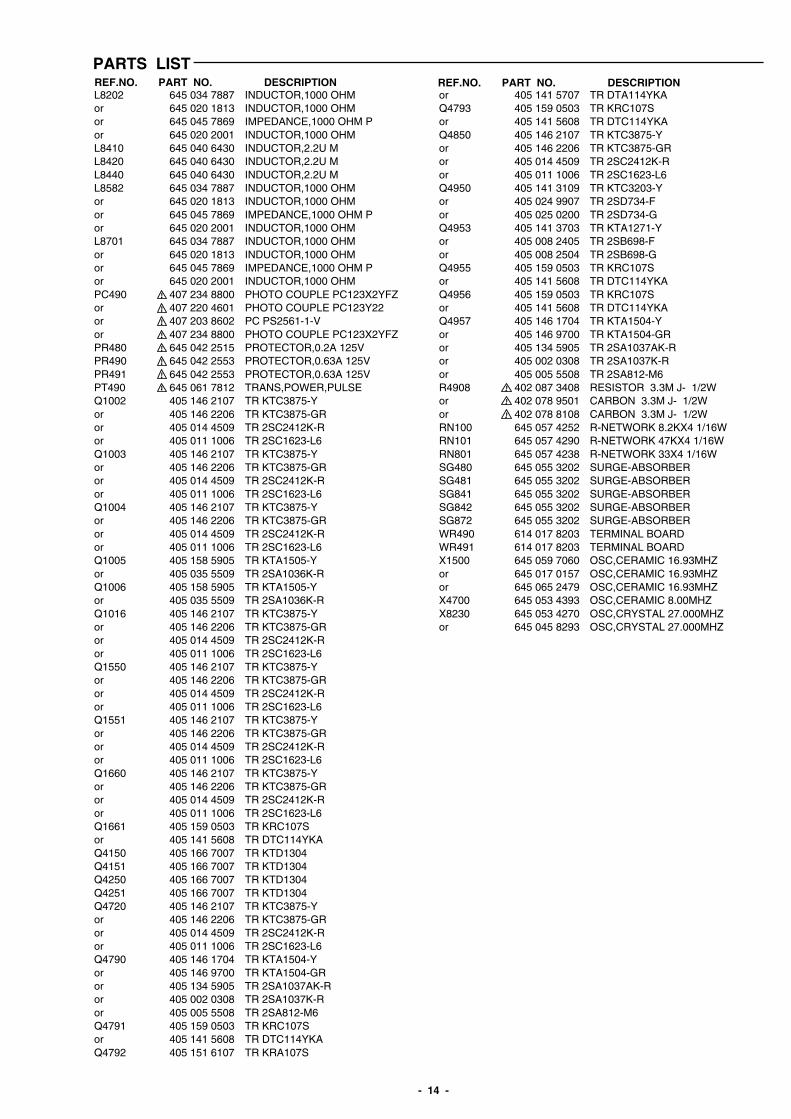
L8202 645 034 7887 INDUCTOR,1000 OHMor 645 020 1813 INDUCTOR,1000 OHMor 645 045 7869 IMPEDANCE,1000 OHM Por 645 020 2001 INDUCTOR,1000 OHML8410 645 040 6430 INDUCTOR,2.2U ML8420 645 040 6430 INDUCTOR,2.2U ML8440 645 040 6430 INDUCTOR,2.2U ML8582 645 034 7887 INDUCTOR,1000 OHMor 645 020 1813 INDUCTOR,1000 OHMor 645 045 7869 IMPEDANCE,1000 OHM Por 645 020 2001 INDUCTOR,1000 OHML8701 645 034 7887 INDUCTOR,1000 OHMor 645 020 1813 INDUCTOR,1000 OHMor 645 045 7869 IMPEDANCE,1000 OHM Por 645 020 2001 INDUCTOR,1000 OHMPC490 407 234 8800 PHOTO COUPLE PC123X2YFZor 407 220 4601 PHOTO COUPLE PC123Y22or 407 203 8602 PC PS2561-1-Vor 407 234 8800 PHOTO COUPLE PC123X2YFZPR480 645 042 2515 PROTECTOR,0.2A 125VPR490 645 042 2553 PROTECTOR,0.63A 125VPR491 645 042 2553 PROTECTOR,0.63A 125VPT490 645 061 7812 TRANS,POWER,PULSEQ1002 405 146 2107 TR KTC3875-Yor 405 146 2206 TR KTC3875-GRor 405 014 4509 TR 2SC2412K-Ror 405 011 1006 TR 2SC1623-L6Q1003 405 146 2107 TR KTC3875-Yor 405 146 2206 TR KTC3875-GRor 405 014 4509 TR 2SC2412K-Ror 405 011 1006 TR 2SC1623-L6Q1004 405 146 2107 TR KTC3875-Yor 405 146 2206 TR KTC3875-GRor 405 014 4509 TR 2SC2412K-Ror 405 011 1006 TR 2SC1623-L6Q1005 405 158 5905 TR KTA1505-Yor 405 035 5509 TR 2SA1036K-RQ1006 405 158 5905 TR KTA1505-Yor 405 035 5509 TR 2SA1036K-RQ1016 405 146 2107 TR KTC3875-Yor 405 146 2206 TR KTC3875-GRor 405 014 4509 TR 2SC2412K-Ror 405 011 1006 TR 2SC1623-L6Q1550 405 146 2107 TR KTC3875-Yor 405 146 2206 TR KTC3875-GRor 405 014 4509 TR 2SC2412K-Ror 405 011 1006 TR 2SC1623-L6Q1551 405 146 2107 TR KTC3875-Yor 405 146 2206 TR KTC3875-GRor 405 014 4509 TR 2SC2412K-Ror 405 011 1006 TR 2SC1623-L6Q1660 405 146 2107 TR KTC3875-Yor 405 146 2206 TR KTC3875-GRor 405 014 4509 TR 2SC2412K-Ror 405 011 1006 TR 2SC1623-L6Q1661 405 159 0503 TR KRC107Sor 405 141 5608 TR DTC114YKAQ4150 405 166 7007 TR KTD1304Q4151 405 166 7007 TR KTD1304Q4250 405 166 7007 TR KTD1304Q4251 405 166 7007 TR KTD1304Q4720 405 146 2107 TR KTC3875-Yor 405 146 2206 TR KTC3875-GRor 405 014 4509 TR 2SC2412K-Ror 405 011 1006 TR 2SC1623-L6Q4790 405 146 1704 TR KTA1504-Yor 405 146 9700 TR KTA1504-GRor 405 134 5905 TR 2SA1037AK-Ror 405 002 0308 TR 2SA1037K-Ror 405 005 5508 TR 2SA812-M6Q4791 405 159 0503 TR KRC107Sor 405 141 5608 TR DTC114YKAQ4792 405 151 6107 TR KRA107S
or 405 141 5707 TR DTA114YKAQ4793 405 159 0503 TR KRC107Sor 405 141 5608 TR DTC114YKAQ4850 405 146 2107 TR KTC3875-Yor 405 146 2206 TR KTC3875-GRor 405 014 4509 TR 2SC2412K-Ror 405 011 1006 TR 2SC1623-L6Q4950 405 141 3109 TR KTC3203-Yor 405 024 9907 TR 2SD734-For 405 025 0200 TR 2SD734-GQ4953 405 141 3703 TR KTA1271-Yor 405 008 2405 TR 2SB698-For 405 008 2504 TR 2SB698-GQ4955 405 159 0503 TR KRC107Sor 405 141 5608 TR DTC114YKAQ4956 405 159 0503 TR KRC107Sor 405 141 5608 TR DTC114YKAQ4957 405 146 1704 TR KTA1504-Yor 405 146 9700 TR KTA1504-GRor 405 134 5905 TR 2SA1037AK-Ror 405 002 0308 TR 2SA1037K-Ror 405 005 5508 TR 2SA812-M6R4908 402 087 3408 RESISTOR 3.3M J- 1/2Wor 402 078 9501 CARBON 3.3M J- 1/2Wor 402 078 8108 CARBON 3.3M J- 1/2WRN100 645 057 4252 R-NETWORK 8.2KX4 1/16WRN101 645 057 4290 R-NETWORK 47KX4 1/16WRN801 645 057 4238 R-NETWORK 33X4 1/16WSG480 645 055 3202 SURGE-ABSORBERSG481 645 055 3202 SURGE-ABSORBERSG841 645 055 3202 SURGE-ABSORBERSG842 645 055 3202 SURGE-ABSORBERSG872 645 055 3202 SURGE-ABSORBERWR490 614 017 8203 TERMINAL BOARDWR491 614 017 8203 TERMINAL BOARDX1500 645 059 7060 OSC,CERAMIC 16.93MHZor 645 017 0157 OSC,CERAMIC 16.93MHZor 645 065 2479 OSC,CERAMIC 16.93MHZX4700 645 053 4393 OSC,CERAMIC 8.00MHZX8230 645 053 4270 OSC,CRYSTAL 27.000MHZor 645 045 8293 OSC,CRYSTAL 27.000MHZ
- 15 -
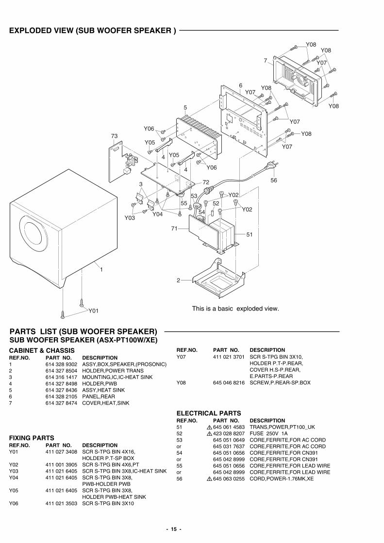
EXPLODED VIEW (SUB WOOFER SPEAKER )
1
2
Y01
Y02Y03
Y04
Y05
Y05
Y06
Y06
Y08
Y08
Y08Y08
Y08
Y07
Y07
Y07
Y07
Y02
71
72
73
51
5253
55
54
563
4
4
5
6
7
PARTS LIST (SUB WOOFER SPEAKER)SUB WOOFER SPEAKER (ASX-PT100W/XE)
This is a basic exploded view.
REF.NO. PART NO. DESCRIPTIONCABINET & CHASSISREF.NO. PART NO. DESCRIPTION1 614 328 9302 ASSY,BOX,SPEAKER,(PROSONIC)2 614 327 8504 HOLDER,POWER TRANS3 614 316 1417 MOUNTING,IC,IC-HEAT SINK4 614 327 8498 HOLDER,PWB5 614 327 8436 ASSY,HEAT SINK6 614 328 2105 PANEL,REAR7 614 327 8474 COVER,HEAT,SINK
FIXING PARTSREF.NO. PART NO. DESCRIPTIONY01 411 027 3408 SCR S-TPG BIN 4X16,
HOLDER P.T-SP BOXY02 411 001 3905 SCR S-TPG BIN 4X6,PTY03 411 021 6405 SCR S-TPG BIN 3X8,IC-HEAT SINKY04 411 021 6405 SCR S-TPG BIN 3X8,
PWB-HOLDER PWBY05 411 021 6405 SCR S-TPG BIN 3X8,
HOLDER PWB-HEAT SINKY06 411 021 3503 SCR S-TPG BIN 3X10
ELECTRICAL PARTSREF.NO. PART NO. DESCRIPTION51 645 061 4583 TRANS,POWER,PT100_UK52 423 028 8207 FUSE 250V 1A53 645 051 0649 CORE,FERRITE,FOR AC CORDor 645 031 7637 CORE,FERRITE,FOR AC CORD54 645 051 0656 CORE,FERRITE,FOR CN391or 645 042 8999 CORE,FERRITE,FOR CN39155 645 051 0656 CORE,FERRITE,FOR LEAD WIREor 645 042 8999 CORE,FERRITE,FOR LEAD WIRE56 645 063 0255 CORD,POWER-1.76MK,XE
Y07 411 021 3701 SCR S-TPG BIN 3X10,HOLDER P.T-P.REAR,COVER H.S-P.REAR,E.PARTS-P.REAR
Y08 645 046 8216 SCREW,P.REAR-SP.BOX

- 16 -
PARTS LISTREF.NO. PART NO. DESCRIPTIONPOWER TRANSFORMER P.W.BOARD ASSY
REF.NO. PART NO. DESCRIPTION71 614 327 4308 ASSY,PWB,MAIN,PT(Only initial)C3900 403 349 3303 CERAMIC 0.01U M 250Vor 403 366 7803 CERAMIC 0.01U M 250VCN390 614 020 1239 SOCKET,4PCN391 614 328 1993 ASSY,WIRED3900 407 012 4406 DIODE 1SS133FPC38 645 031 7903 HOLDER,FUSEor 645 006 4760 HOLDER,FUSEFPC39 645 031 7903 HOLDER,FUSEor 645 006 4760 HOLDER,FUSEL3900 645 038 7364 INDUCTOR,70Uor 645 059 0467 INDUCTOR,13ULUG01 645 006 4425 FIXERRY390 645 059 0306 RELAY,PRIMARYor 645 030 5597 RELAY,PRIMARYor 645 035 6575 RELAY,PRIMARYWR390 614 017 8203 TERMINAL BOARDWR391 614 017 8203 TERMINAL BOARD
MAIN P.W.BOARD ASSYREF.NO. PART NO. DESCRIPTION72 614 329 5105 ASSY,PWB,MAIN(Only initial)C3004 403 325 0302 ELECT 2200U M 25VC3008 403 325 0302 ELECT 2200U M 25VC3210 403 184 9805 MT-POLYEST 0.22U J 50VC3211 403 184 9805 MT-POLYEST 0.22U J 50VC3213 403 184 9805 MT-POLYEST 0.22U J 50VC3214 403 184 9805 MT-POLYEST 0.22U J 50VC3405 403 185 0108 MT-POLYEST 0.47U J 50VC3406 403 185 0108 MT-POLYEST 0.47U J 50VC3408 403 184 9300 MT-POLYEST 0.047U J 50VCN302 645 006 1790 PLUG,2PCN303 645 005 7366 PLUG,2PCN305 645 063 4864 PLUG,10PCN311 645 006 1813 PLUG,4PD3000 407 099 6805 ZENER DIODE MTZJ13BD3001 407 099 6805 ZENER DIODE MTZJ13BD3002 407 196 5800 DIODE 1N5402BD82D3003 407 196 5800 DIODE 1N5402BD82D3004 407 196 5800 DIODE 1N5402BD82D3005 407 196 5800 DIODE 1N5402BD82D3501 407 012 4406 DIODE 1SS133D3502 407 012 4406 DIODE 1SS133IC320 409 472 5306 IC LM1876TFIC330 409 426 1903 IC KIA4558For 409 039 7804 IC NJM4558MIC340 409 521 9200 IC LM4700TFIC360 409 039 5404 IC NJM2058ML3200 645 057 4405 INDUCTOR,0.7Uor 645 053 7493 INDUCTOR,0.7UL3201 645 057 4405 INDUCTOR,0.7Uor 645 053 7493 INDUCTOR,0.7UL3400 645 057 7673 INDUCTOR,AIR 0.7Uor 645 045 6206 INDUCTOR,AIR 0.7UPR300 645 042 2515 PROTECTOR,0.2A 125VPR301 645 042 2515 PROTECTOR,0.2A 125VPR302 645 042 2652 PROTECTOR,10A 125VPR303 645 042 2652 PROTECTOR,10A 125VQ3000 405 143 0007 TR KRC107Mor 405 000 3806 TR DTC114YSQ3001 405 141 3505 TR KTA1266-Yor 405 141 3406 TR KTA1266-GRor 405 004 4502 TR 2SA608-F-NPor 405 004 5004 TR 2SA608-G-NPQ3002 405 141 3208 TR KTC3198-Yor 405 141 3307 TR KTC3198-GRor 405 019 2708 TR 2SC536-F-NPor 405 019 3804 TR 2SC536-G-NPQ3003 405 143 0007 TR KRC107Mor 405 000 3806 TR DTC114YS
TERMINAL P.W.BOARD ASSYREF.NO. PART NO. DESCRIPTION73 614 329 5112 ASSY,PWB,TERMINAL(Only initial)CN370 645 063 9098 JACK,PHONE D3.6CN371 645 061 6990 TERMINAL,SPEAKER 2PCN372 645 006 1882 PLUG,3PCN373 645 005 8493 SOCKET,10PL3700 645 006 3602 INDUCTOR,1.1UHL3701 645 006 3602 INDUCTOR,1.1UHL3702 645 006 3602 INDUCTOR,1.1UHL3703 645 006 3602 INDUCTOR,1.1UH
Q3200 405 151 4400 TR KTD1303or 405 021 0204 TR 2SD1012-F-SPAor 405 021 0600 TR 2SD1012-G-SPAor 405 033 6706 TR 2SD1468S-Ror 405 033 6805 TR 2SD1468S-SQ3201 405 151 4400 TR KTD1303or 405 021 0204 TR 2SD1012-F-SPAor 405 021 0600 TR 2SD1012-G-SPAor 405 033 6706 TR 2SD1468S-Ror 405 033 6805 TR 2SD1468S-SQ3400 405 151 4400 TR KTD1303or 405 021 0204 TR 2SD1012-F-SPAor 405 021 0600 TR 2SD1012-G-SPAor 405 033 6706 TR 2SD1468S-Ror 405 033 6805 TR 2SD1468S-SQ3500 405 141 3208 TR KTC3198-Yor 405 141 3307 TR KTC3198-GRor 405 019 2708 TR 2SC536-F-NPor 405 019 3804 TR 2SC536-G-NPQ3501 405 141 3208 TR KTC3198-Yor 405 141 3307 TR KTC3198-GRor 405 019 2708 TR 2SC536-F-NPor 405 019 3804 TR 2SC536-G-NPR3210 402 082 1300 RESISTOR 4.7 J- 1WR3211 402 082 1300 RESISTOR 4.7 J- 1WR3212 402 082 2802 RESISTOR 10 J- 1WR3213 402 082 2802 RESISTOR 10 J- 1WR3405 402 082 8606 RESISTOR 2.2 J- 1WR3406 402 082 2802 RESISTOR 10 J- 1W
- 17 -
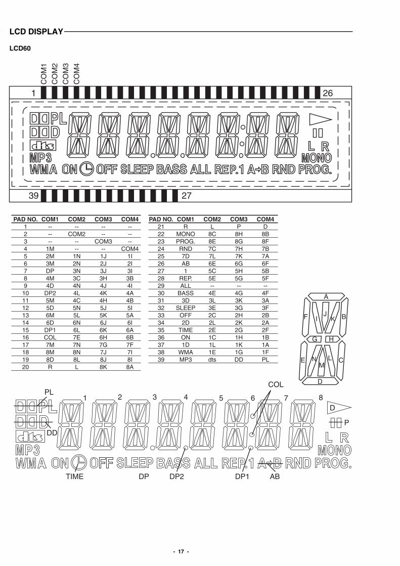
LCD DISPLAY
LCD60
1 26
2739
1 2 3 4 5 6 7 8
A
B
C
D
E
F
G H
IJ
K
LM
N
PAD NO.1 2 3 4 5 6 7 8 9
10 11 12 13 14 15 16 17 18 1920
PAD NO.21 22 23 24 25 26 27 28 29 30 31 32 33 34 35 36 37 38 39
COM1 -- -- --
1M 2M 3M DP 4M 4D
DP2 5M 5D 6M 6D
DP1 COL 7M 8M 8D R
COM2 --
COM2 -- --
1N 2N 3N 3C 4N4L 4C 5N 5L 6N 6L7E 7N 8N 8L L
COM3-- --
COM3 -- 1J 2J 3J3H 4J 4K 4H 5J 5K 6J 6K 6H 7G 7J 8J 8K
COM4-- -- --
COM4 1I 2I 3I 3B 4I 4A 4B 5I 5A 6I 6A 6B 7F 7I 8I 8A
COM4D 8B 8F 7B 7A 6F 5B 5F -- 4F3A 3F 2B 2A 2F 1B 1A 1F PL
COM3P
8H 8G 7H 7K 6G 5H 5G --
4G3K 3G 2H 2K 2G 1H 1K 1G DD
COM2 L
8C8E 7C 7L 6E 5C 5E --
4E3L 3E 2C 2L 2E 1C 1L 1E dts
COM1 R
MONOPROG.RND7DAB1
REP.ALL
BASS3D
SLEEPOFF2D
TIMEON1D
WMAMP3
CO
M1
CO
M2
CO
M3
CO
M4
COLPL
DD
D
DP DP1DP2
P
TIME AB
- 18 -
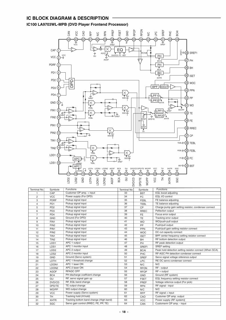
IC BLOCK DIAGRAM & DESCRIPTIONIC100 LA9703WL-MPB (DVD Player Frontend Processor)
APC
LPF1
LPF2
LPF1
BPF
BH
PH
PH
DOOUT
LPF2
DP
D
EQ
APCTEBL
TEBL
LDTH
LDT
H
LDON1
LDON1
LDON2LDON2
AGOF
SREF
BCA GU
GU
GU
GU
GU
SGC
XHTR
SREF
SREF
SR
EF
1
SREF
XHTR
XHTR
DPD/TE
WO/PP
SREF
SGC
SREF
SREF
FEBL
PREF
PREF
FEBL
DVD/CD DPD/TE WO/PP VCC TH
TH
XHTR SGC
SGC
SGC
BST
FC
FEBL
TEBL
BCA
BCA
BCA
FC BSTDVD/CD
VCC
VCC
PREF
AGOF
AGOF
GU
1
2
3
4
5
6
7
8
9
10
11
12
13
14
15
16
17 18 19 20 21 22 23 24 25 27 28 29 30 31 32
33
34
35
36
37
38
39
40
41
42
43
44
45
46
47
48
495051525354555657596061626364 58
26
SREF1
PH
BH
ISET
WOC
PPN
PP
WO
TE
FE
RREC
TEBL
CP
FEBL
FC
BST
SGC
XHTRTH
VCC
WO
/PP
DPD
/TE
DVD
/CD
GU
BCA
AGO
F
LDO
N2
LDO
N1
LDTH
GN
D
LDS2
LDD
2
LDS1
LDD1
TIN2
TIN1
PIN2
PIN1
FIN2
FIN1
GND
PD4
PD3
PD2
PD1
PDRF
VCC
CAP
BCAI
PHC
SREF
LPC
N/C
RFO
N
RFO
P
GN
D
FSET
PREF
RFN
RFP
CAO
VCC
CAN
N/C
FunctionsCustomer OP amp. + inputPower supply (For DPD)Pickup signal inputPickup signal inputPickup signal inputPickup signal inputPickup signal inputGround (For DPD)Pickup signal inputPickup signal inputPickup signal inputPickup signal inputPickup signal inputPickup signal inputAPC 1 outputAPC 1 monitor inputAPC 2 outputAPC 2 monitor inputGround (Servo system)APC 1 threshold changeAPC 1 laser ONAPC 2 laser ONRFAGC OFFPH discharge coeffcient changeRF, servo signal gain upRF, EQL band changeTE output changeWO output changePower supply (Servo system)Tracking hold (H:hold)Tracking bottom band change (High band)Servo gain control (RREC, FE, PP, TE)
Terminal No.123456789
1011121314151617181920212223242526272829303132
SymboleCAPVCCPDRFPD1PD2PD3PD4GNDFIN1FIN2PIN1PIN2TIN1TIN2LDD1LDS1LDD2LDS2GNDLDTHLDON1LDON2AGOFBCAGUDVD/CDDPD/TEWO/PPVCCTHXHTRSGC
Terminal No Symbole Functions3334353637383940414243444546474849505152535455565758596061626364
BSTFCFEBLTEBLCPRRECFETEWOPPPPNWOCISETBHPHSREFIBCAIPHCSREFLPCN/CRFONRFOPGNDFSETPREFRFNN/CRFPCAOVCCCAN
EQL boost adjustingEQL I/O controlFE balance adjustingTE balance adjustingCharge pump gain setting resistor, condenser connectPeflection outputFocus error outputTracking error outputWO/push-pull outputPush/pull outputPush/pull gain setting resistor connectDC cut capacity connectBPF center frequency setting resistor connectRF bottom detection outputRF peak detection outputSREF settingPeak hold detection setting resistor connect (When SCA)RF-AGC PH detection conderser connectServo signal voltage reference outputRE DC servo condenser connectN/CRF - outputRF + outputGround (RF system)EQL frequency setting resistor connectVoltage refernce output (For pick)RF signal - inputN/CRF signal + inputCustomer OP amp. outputPower supply (RF system)[Customerm OP amp. - input
- 19 -
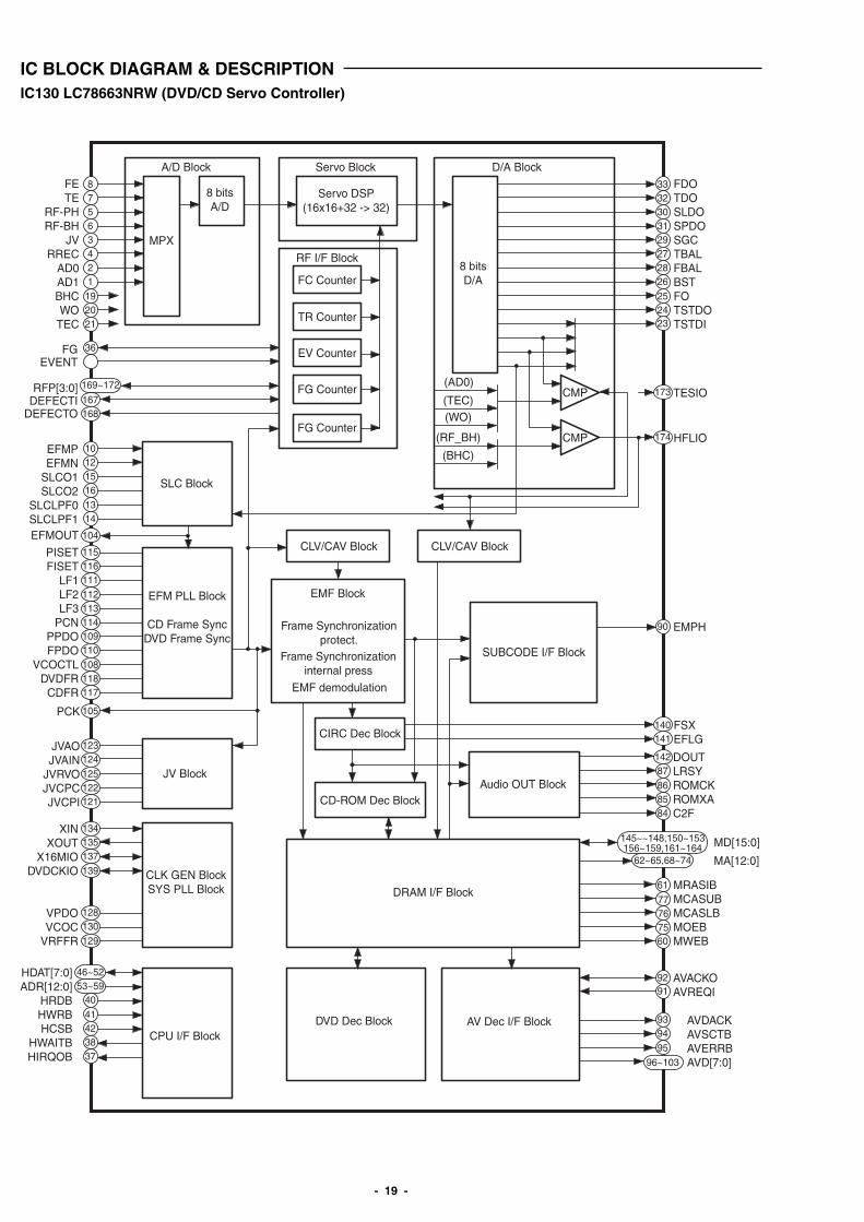
IC BLOCK DIAGRAM & DESCRIPTIONIC130 LC78663NRW (DVD/CD Servo Controller)
87563421192021
3332303129272826252423
36
167168
1516
1012
1314
104
115116111112113114109110108
134135137139
128130129
145~~148,150~153156~159,161~164
62~65,68~74
140141
174
173
90
61
77
14287868584
767560
46~5253~59
169~172
4041423837
9493
9291
9596~103
118117
123124125122121
105
FETE
RF-PHRF-BH
JVRREC
AD0AD1BHCWO
TEC
FGEVENT
RFP[3:0]DEFECTI
DEFECTO
EFMPEFMN
SLCO1SLCO2
SLCLPF0SLCLPF1EFMOUT
PISETFISET
LF1LF2LF3
PCNPPDOFPDO
VCOCTLDVDFR
CDFR
PCK
JVAOJVAIN
JVRVOJVCPCJVCPI
XINXOUT
X16MIODVDCKIO
VPDOVCOC
VRFFR
HDAT[7:0]ADR[12:0]
HRDBHWRBHCSB
HWAITBHIRQOB
FDOTDOSLDOSPDOSGCTBALFBALBSTFOTSTDOTSTDI
TESIO
HFLIO
EMPH
FSXEFLG
DOUTLRSYROMCKROMXAC2F
MRASIBMCASUBMCASLBMOEBMWEB
MD[15:0]
MA[12:0]
AVACKOAVREQI
AVDACKAVSCTBAVERRBAVD[7:0]
A/D Block D/A BlockServo Block
SLC Block
8 bitsA/D
8 bitsD/A
Servo DSP(16x16+32 -> 32)
MPX
RF I/F Block
FC Counter
TR Counter
EV Counter
FG Counter
FG Counter
(AD0)
(TEC)(WO)
(RF_BH)
(BHC)
CMP
CMP
CLV/CAV Block CLV/CAV Block
SUBCODE I/F Block
EFM PLL Block
CD Frame SyncDVD Frame Sync
JV Block
CLK GEN BlockSYS PLL Block
CPU I/F BlockDVD Dec Block AV Dec I/F Block
DRAM I/F Block
CD-ROM Dec Block
CIRC Dec Block
Audio OUT Block
EMF Block
Frame Synchronizationprotect.
Frame Synchronizationinternal press
EMF demodulation

- 20 -
IC BLOCK DIAGRAM & DESCRIPTIONIC130 LC78663NRW (DVD/CD Servo Controller)
NO.123456789101112131415161718192021222324252627282930313233343536373839404142434445464748495051525354555657585960616263646566
67
68697071727374757677787980818283
848586
87
BROCK A/D
Test tarminal SLCTest tarminal
Power supply
CMP
D/A
Power supply RF I/F Micro- computer I/F
Power supply Micro- computer I/F
DRAM I/F
NC
DRAM I/F
Micro- computer I/F
CD data
NAMEAD1AD0JVRRECRF-PHRF-BHTEFETEST0EFMINPTEST1EFMINNSLCLPF0SLCLPF1SLCO1SLCO2AVDDIAVSSBHCWOTECVREFTSTDITSTDOFOBSTTBALFBALSGCSLDOSPDOTDOFDODVDD0DVSSFGHIRQBHWAITBHRESBHRDBHWRBHCSBHDATODVDD1DVSSHDAT1HDAT2HDAT3HDAT4HDAT5HDAT6HDAT7HADR0HADR1HADR2HADR3HADR4HADR5HADR6MWEBMRASIBMA0MA1MA2MA3NC
NC
MA4MA5MA6MA7MA8MA9MA10MOEBMCASUBMCASLBHADR7HADR8HADR9HADR10HADR11HADR12
C2FROMXAROMCK
LRSY
SUPPLEMENTSurvo A/D AD1Survo A/D AD0Survo A/D JVSurvo A/D RRECSurvo A/D RF_PHSurvo A/D RF_BHSurvo A/D TESurvo A/D FETest input 0(Input: "L" level fixed)EFM/EFMI inputTest input 1(Input: "L" level fixed)EFM- InputSLCSLCSLCSLCA/D D/A SLC power supply(Analog 3.3V)Analog GNDComparator input(RF_BH C)Comparetor inputComparetor input(TE C)Survo D/A voltage referenceSurvo D/ASurvo D/A TSTDOSurvo D/A FOSurvo D/A BSTSurvo D/A TBALSurvo D/A FBALSurvo D/A SGCSurvo D/A SLDOSurvo D/A SPDOSurvo D/A TDOSurvo D/A FDOPower supply for internal logic(Digital 2.5V)Digital GNDFG counter input General port I/O 1Interrupt signal outputWait signal outputSurvo reset inputRead signal inputWrite signsl inputChip select signsl inputData bus OI/O power supply(Digital 3.3V)Digital GNDData bus 1Data bus 2Data bus 3Data bus 4Data bus 5Data bus 6Data bus 7Address bus 0Address bus 1Address bus 2Address bus 3Address bus 4Address bus 5Address bus 6WE outputRAS outout 1DRAM address bus 0DRAM address bus 1DRAM address bus 2DRAM address bus 3NC Pin which fixed "H" or "L"(662:DRAM power supply[Digital 3.3V])NCPin which fixed "H" or "L"(662:Digital GND)DRAM address bus 4DRAM address bus 5DRAM address bus 6DRAM address bus 7DRAM address bus 8DRAM address bus 9DRAM address bus 10OE outputCAS output(Upper byte)CAS output(Low byte)Address bus 7Address bus 8Address bus 9Address bus 10Address bus 11Address bus 12 Buffer memory access selector[MCSB]C2 frag output Monitor 4CD data output Monitor 3Sift clock output for CD data Monitor 2outputL/R clock output for CD data Monitor 1output
SUPPLEMENTI/O power supply[Digital 3.3V]Digital GNDDE-EMP monitor Monitor 0AV data requirement flag inputAV data read strobe outputAV data read outputAV output sector synchronous output AV dta reliability flag outputAV data bus 0AV data bus 1AV data bus 2AV data bus 3AV data bus 4AV data bus 5AV data bus 6AV data bus 7EFM 2 value signsl outputEFM playback shift clock outputInternal logic power suuply(Digital 2.5V)Digital GNDVCO filter connectPhase comparison filter connectFrequency comparison filter connectFilter connect 1Filter connect 2Filter connect 3Voltaji moniter(Charge pump PCH control voltage)Constant-current charge pump current set of phase comparisonConstant-current charge pump current set of frequency comparisonEFM playback PLL VCO oscillation renge set[CD]EFM playback PLL VCO oscillation range set[DVD]EFM PLL, JV power supply[Analog 3.3V]Analog GNDJVJVEFM playback PLL clock jitter outputJVJVSystem PLL power supply[Analog 2.5V]Analog GNDSystem PLL filter connectSystem PLL VCO oscillation range sotSystem PLL filter connectInternal logic power supply[Digital 2.5V]Digital GNDOscillation circuit power supply[Digital 3.3V]Oscillation circuit inputOscillation circuit outputDigital GNDExternal 16MHz input and outputTest input 2[Input "L" level setting]External DVD clock input and outputCD1 frame synchronous signal Monitor 6C1 and C2 correction state Monitor 5Audio EIAJ data output Monitor 7I/O power supply[Digital 3.3V]Digital GNDDRAM data bus 8DRAM data bus 9DRAM data bus 10DRAM data bus 11NC pin which fixed "H" or "L"(662:Digital GND)DRAM data bus 12DRAM data bus 13DRAM data bus 14DRAM data bus 15NC pin which fixed "H" or "L"(662:Digital GND)NC pin which fixed "H" or "L"(662:DRAM power supply[Digital 3.3V])DRAM data bus 0DRAM data bus 1DRAM data bus 2DRAM data bus 3NC pin which fixed "H" or "L"(662:DRSM power supply[Digital3.3V])DRAM data bus 4DRAM data bus 5DRAM data bus 6DRAM data bus 7I/O power supply[Digital 3.3V]Digital GNDDefect signal input General port I/O 0Defect signal outputRF general port I/O 0 WRQ outputRF general port I/O 1RF general port I/O 2 HBUSYB outputRF general port I/O 3 HFBUSYB output EVENT counter inputTrucking error signal I/OMirror detection signal I/OInternal logic power supply[Digital 2.5V]Digital GND
I/OIIIIIIIIIIII------IIIOOOOOOOOOOOO--
I/OOOIIII
I/O-
I/OI/OI/OI/OI/OI/OI/OIIIIIIIOOOOOO-
-
OOOOOOOOOOIIIIII
OOO
O
NO.888990919293949596979899100101102103104105106107108109110111112113114115116117118119120121122123124125126127128129130131132133134135136137138139140141142143144145146147148149150151152153154155
156157158159160
161162163164165166167168169170171172
173174175176
BLOCK
CD dataAV data I/F
RF I/F
Powersupply
EFMPLL
PowersupplyJV
PowersupplySystem CLK
PowersupplyPower supplySystem CLKPower supplySystem CLK
Monitor
CD dataPowersupplyDRAM I/F
NCDRAM I/F
NC
DRAM I/F
NC
DRAM I/F
Powersupply
RF I/F
Powersupply
NAMEDVDD1DVSSEMPHAVREQIAVACKOAVDACKAVSCTBAVERRBAVD0AVD1AVD2AVD3AVD4AVD5AVD6AVD7EFMOUTPCKDVDD0DVSSVCOCTLPPDOFPDOLF1LF2LF3PCSPISETFISETCDFRDVDFRAVDD2AVSSJVCPIJVCPCJVAOJVAINJVRVOAVDD3AVSSVPDOVRPFRVCOCDVDD0DVSSDVDD2XINXOUTDVSSX16M10TEST2DVDCK10FSXEFLGDOUTDVDD1DVSSMD8MD9MD10MD11NCMD12MD13MD14MD15NCNC
MD0MD1MD2MD3NC
MD4MD5MD6MD7DVDD1DVSSDEFECT1DEFECT0RFP0RFP1RFP2RFP3
TESIOHFLIODVDD0DVSS
I/O--OIOOOOOOOOOOOOOO-----------------O----------IO-
I/OI
I/OOOO--
I/OI/OI/OI/O-
I/OI/OI/OI/O--
I/OI/OI/OI/O-
I/OI/OI/OI/O
I/OO
I/OI/OI/OI/O
I/OI/O- -
- 21 -
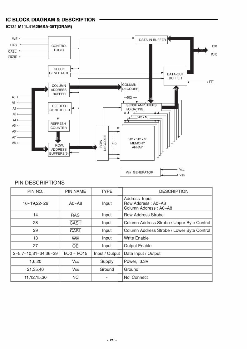
PIN DESCRIPTIONS
PIN NO. PIN NAME TYPE DESCRIPTION
16~19,22~26 A0~A8 InputAddress InputRow Address : A0~A8Column Address : A0~A8
14 RAS Input Row Address Strobe
28 CASH Input Column Address Strobe / Upper Byte Control
29 CASL Input Column Address Strobe / Lower Byte Control
13 WE Input Write Enable
27 OE Input Output Enable
2~5,7~10,31~34,36~39 I/O0 ~ I/O15 Input / Output Data Input / Output
1,6,20 VCC Supply Power, 3.3V
21,35,40 VSS Ground Ground
11,12,15,30 NC - No Connect
CONTROL LOGIC
DATA-IN BUFFER
CLOCKGENERATOR DATA-OUT
BUFFER
COLUMNADDRESS BUFFER
REFRESHCONTROLER
REFRESHCOUNTER
ROW. ADDRESSBUFFERS(9)
9
A0
A1
A2
A3
A4
A5
A6
A7
COLUMNDECODER
OE
16
R
OW
DE
CO
DE
R
512 x 512 x 16 MEMORY ARRAY
16
SENSE AMPLIFIERSI/O GATING 8
512 x 16
VCC
VSS
IO0 :IO15
RAS
CASH
512
512
99
9 9
9
CASL
VBB GENERATOR
WE
16
A8
IC BLOCK DIAGRAM & DESCRIPTIONIC131 M11L416256SA-35T(DRAM)
- 22 -
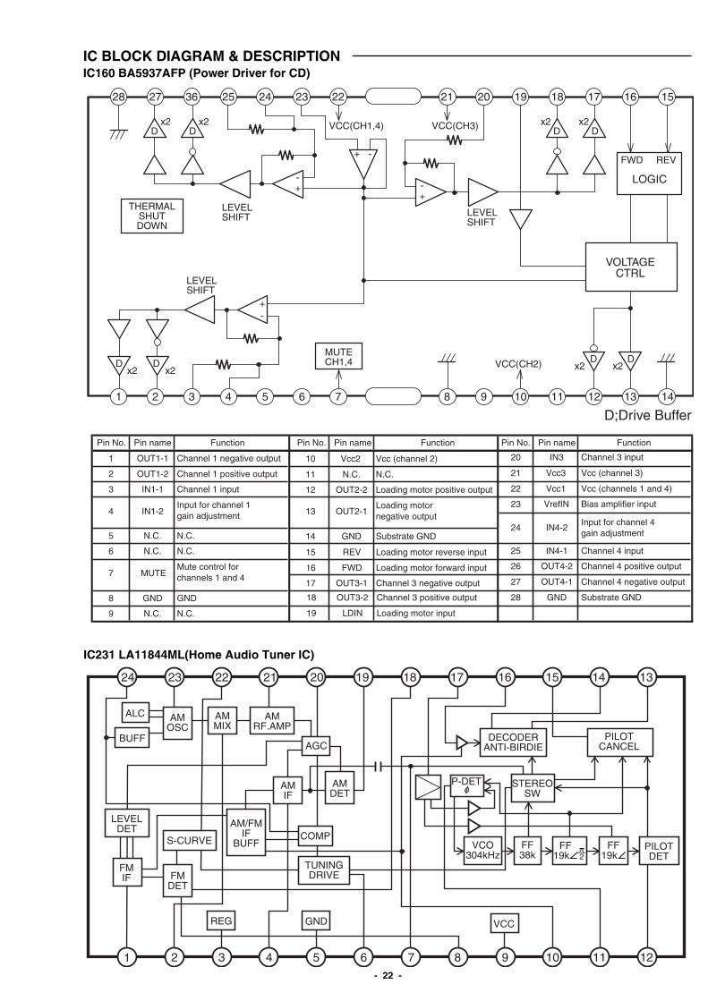
IC BLOCK DIAGRAM & DESCRIPTIONIC160 BA5937AFP (Power Driver for CD)
1 2 3 4 5 6 7 8 9 10 11 12 13 14
28 27 36 25 24 23 22 21 20 19 18 17 16 15
+
+
+
-
-
+-
-
D
D D
x2D
x2
x2 x2D Dx2 x2
Dx2
Dx2
LEVELSHIFT
LEVELSHIFT LEVEL
SHIFT
VCC(CH3)VCC(CH1,4)
VCC(CH2)
THERMALSHUTDOWN
MUTECH1,4
FWD REV
LOGIC
VOLTAGECTRL
Pin No. Pin name Function Pin No. Pin name Function Pin No. Pin name Function
1 OUT1-1 Channel 1 negative output
15 REV Loading motor reverse input
2 OUT1-2 Channel 1 positive output
16 FWD Loading motor forward input
3 IN1-1 Channel 1 input
17 OUT3-1 Channel 3 negative output
4 IN1-2Input for channel 1gain adjustment
18 OUT3-2 Channel 3 positive output
5 N.C. N.C.
19 LDIN Loading motor input
6 N.C. N.C.
20 IN3 Channel 3 input
7 MUTEMute control forchannels 1 and 4
21 Vcc3 Vcc (channel 3)
8 GND GND
22 Vcc1 Vcc (channels 1 and 4)
9 N.C. N.C.
23 VrefIN Bias amplifier input
10 Vcc2 Vcc (channel 2)
24 IN4-2Input for channel 4gain adjustment
11 N.C. N.C.
25 IN4-1 Channel 4 input
12 OUT2-2 Loading motor positive output
26 OUT4-2 Channel 4 positive output
13 OUT2-1Loading motornegative output
27 OUT4-1 Channel 4 negative output
14 GND Substrate GND
28 GND Substrate GND
D;Drive Buffer
FMIF FM
DET
LEVELDET
S-CURVE
AM/FMIF
BUFF
REG GND
COMP
TUNINGDRIVE
AMIF
AMDET
VCC
AGCPILOT
CANCEL
PILOTDET
DECODERANTI-BIRDIE
STEREOSW
FF38k
FF19k
VCO304kHz
AMRF.AMP
AMMIX
AMOSC
ALC
BUFF
P-DET
FF19k 2
1 2 3 4 5 6 7 8 9 10 11 12
24 23 22 21 20 19 18 17 16 15 14 13
IC231 LA11844ML(Home Audio Tuner IC)
- 23 -
IC BLOCK DIAGRAM & DESCRIPTION
Pin No.1234567891011121314
Pin No.1516171819202122232425262728
Output
Output
OutputGNDHall signsl inputHall signal inputHall signal inputHall signal inputHall signal inputHall signal input
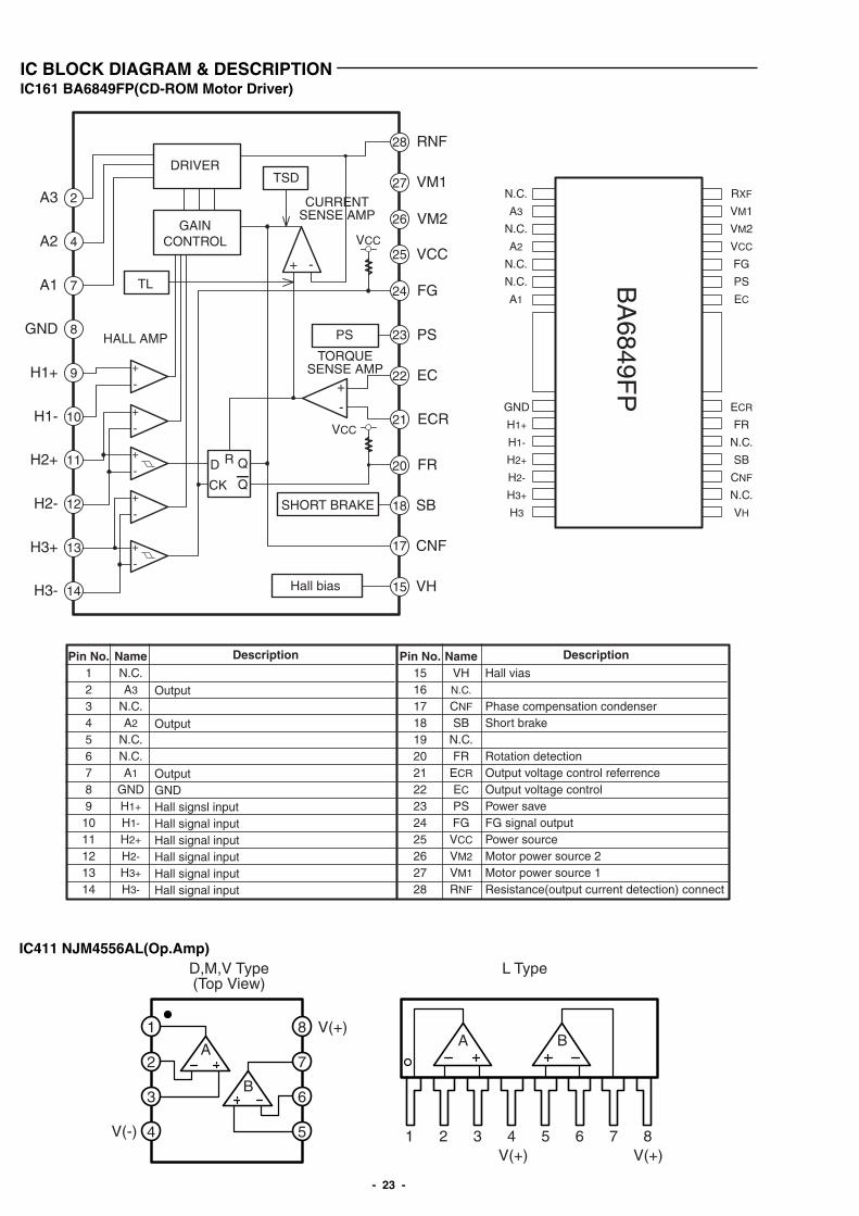
Description DescriptionNameN.C.A3
N.C.A2
N.C.N.C.A1
GNDH1+
H1-
H2+
H2-
H3+
H3-
NameVHN.C.
CNF
SBN.C.FR
ECR
EC
PSFGVCC
VM2
VM1
RNF
Hall vias
Phase compensation condenserShort brake
Rotation detectionOutput voltage control referrenceOutput voltage controlPower saveFG signal outputPower sourceMotor power source 2Motor power source 1Resistance(output current detection) connect
N.C.
A3
N.C.
A2
N.C.
N.C.
A1
RXF
VM1
VM2
VCC
FG
PS
EC
ECR
FR
N.C.
SB
CNF
N.C.
VH
GND
H1+
H1-
H2+
H2-
H3+
H3
BA
6849FP
IC161 BA6849FP(CD-ROM Motor Driver)
A3
RNF
VM1
VM2
VCC
FG
PS
EC
ECR
FR
SB
CNF
VH
A2
A1
GND
H1+
H1-
H2+
H2-
H3+
H3-
2
28
27
26
25
24
23
22
21
20
18
17
15
4
7
8
9
10
11
12
13
14
+
-
+
-
+
-
+
-
+ -
+
-
+
-
DRIVER
GAINCONTROL
TSD
TL
PS
SHORT BRAKE
Hall bias
D R Q
QCK
VCC
VCC
HALL AMPTORQUE
SENSE AMP
CURRENTSENSE AMP
IC411 NJM4556AL(Op.Amp)
1
2
3
4
8
7
6
5 1 2 3 4 5 6 7 8
A
B
A B
D,M,V Type(Top View)
L Type
V(+)
V(+)V(+)
V(-)
- 24 -
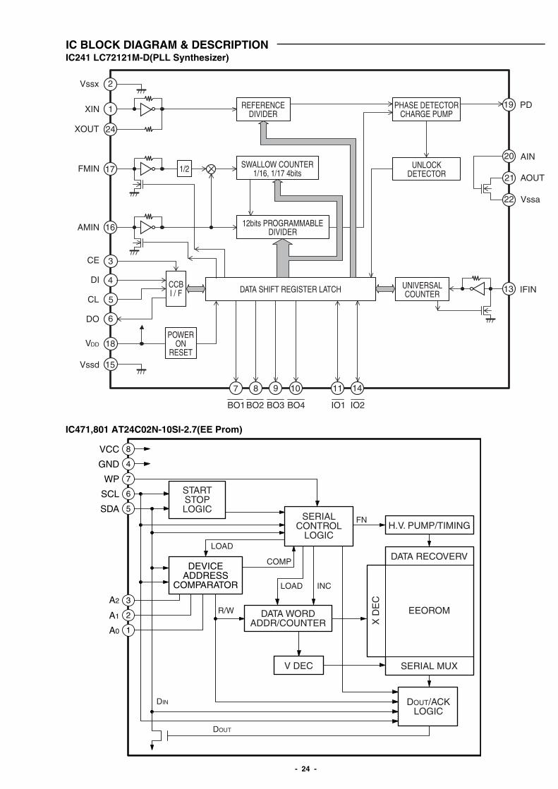
IC471,801 AT24C02N-10SI-2.7(EE Prom)
8VCC
4GND
7WP
3A2
2A1
1A0
6SCL
5SDA
DEVICEADDRESS
COMPARATOR
STARTSTOPLOGIC
SERIALCONTROL
LOGICH.V. PUMP/TIMING
DATA RECOVERV
EEOROM
SERIAL MUX
DOUT/ACKLOGIC
V DEC
DATA WORDADDR/COUNTER
R/W
DIN
DOUT
LOAD INC
COMP
LOAD
FN
X D
EC
IC BLOCK DIAGRAM & DESCRIPTION
2
1
24
17
16
3
4
5
6
18
15
7 8 9 10 11 14
19
20
21
22
13
Vssx
XIN
XOUT
FMIN
AMIN
CE
DI
CL
DO
VDD
Vssd
PD
AIN
AOUT
Vssa
IFIN
IO1 IO2BO1BO2 BO3 BO4
PHASE DETECTORCHARGE PUMP
UNLOCKDETECTOR
UNIVERSALCOUNTER
REFERENCEDIVIDER
SWALLOW COUNTER1/16, 1/17 4bits
12bits PROGRAMMABLEDIVIDER
DATA SHIFT REGISTER LATCH
1/2
CCBI / F
POWERON
RESET
IC241 LC72121M-D(PLL Synthesizer)
- 25 -
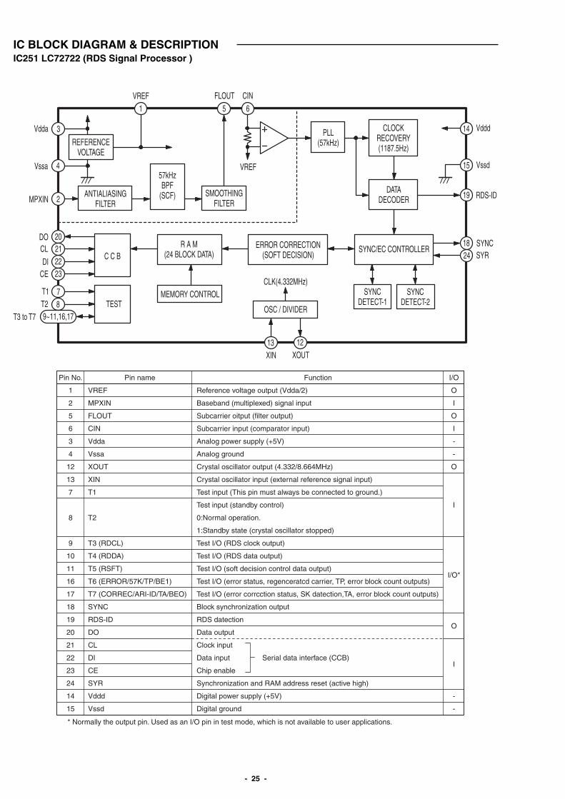
IC BLOCK DIAGRAM & DESCRIPTIONIC251 LC72722 (RDS Signal Processor )
Vdda
REFERENCEVOLTAGE
3
4
2
20212223
78
9~11,16,17
1 5 6
14
15
19
1824
13 12
ANTIALIASINGFILTER
57kHzBPF
(SCF) SMOOTHINGFILTER
VREF
PLL(57kHz)
CLOCKRECOVERY(1187.5Hz)
DATADECODER
SYNC/EC CONTROLLERERROR CORRECTION(SOFT DECISION)
R A M(24 BLOCK DATA)C C B
TESTMEMORY CONTROL
CLK(4.332MHz)
OSC / DIVIDER
SYNCDETECT-1
SYNCDETECT-2
Vssa
MPXIN
DOCLDI
CE
T1T2
T3 to T7
XIN XOUT
Vddd
Vssd
RDS-ID
VREF FLOUT CIN
SYNCSYR
Function
Reference voltage output (Vdda/2)
Baseband (multiplexed) signal input
Subcarrier oitput (filter output)
Subcarrier input (comparator input)
Analog power supply (+5V)
Analog ground
Crystal oscillator output (4.332/8.664MHz)
Crystal oscillator input (external reference signal input)
Test input (This pin must always be connected to ground.)
Test input (standby control)
0:Normal operation.
1:Standby state (crystal oscillator stopped)
Test I/O (RDS clock output)
Test I/O (RDS data output)
Test I/O (soft decision control data output)
Test I/O (error status, regenceratcd carrier, TP, error block count outputs)
Test I/O (error corrcction status, SK datection,TA, error block count outputs)
Block synchronization output
RDS datection
Data output
Clock input
Data input Serial data interface (CCB)
Chip enable
Synchronization and RAM address reset (active high)
Digital power supply (+5V)
Digital ground
I/O
O
I
O
I
-
-
O
I
I/O*
O
I
-
-
Pin name
VREF
MPXIN
FLOUT
CIN
Vdda
Vssa
XOUT
XIN
T1
T2
T3 (RDCL)
T4 (RDDA)
T5 (RSFT)
T6 (ERROR/57K/TP/BE1)
T7 (CORREC/ARI-ID/TA/BEO)
SYNC
RDS-ID
DO
CL
DI
CE
SYR
Vddd
Vssd
Pin No.
1
2
5
6
3
4
12
13
7
8
9
10
11
16
17
18
19
20
21
22
23
24
14
15
* Normally the output pin. Used as an I/O pin in test mode, which is not available to user applications.
- 26 -
IC BLOCK DIAGRAM & DESCRIPTION
Q1Q2
1
5
2 3
4
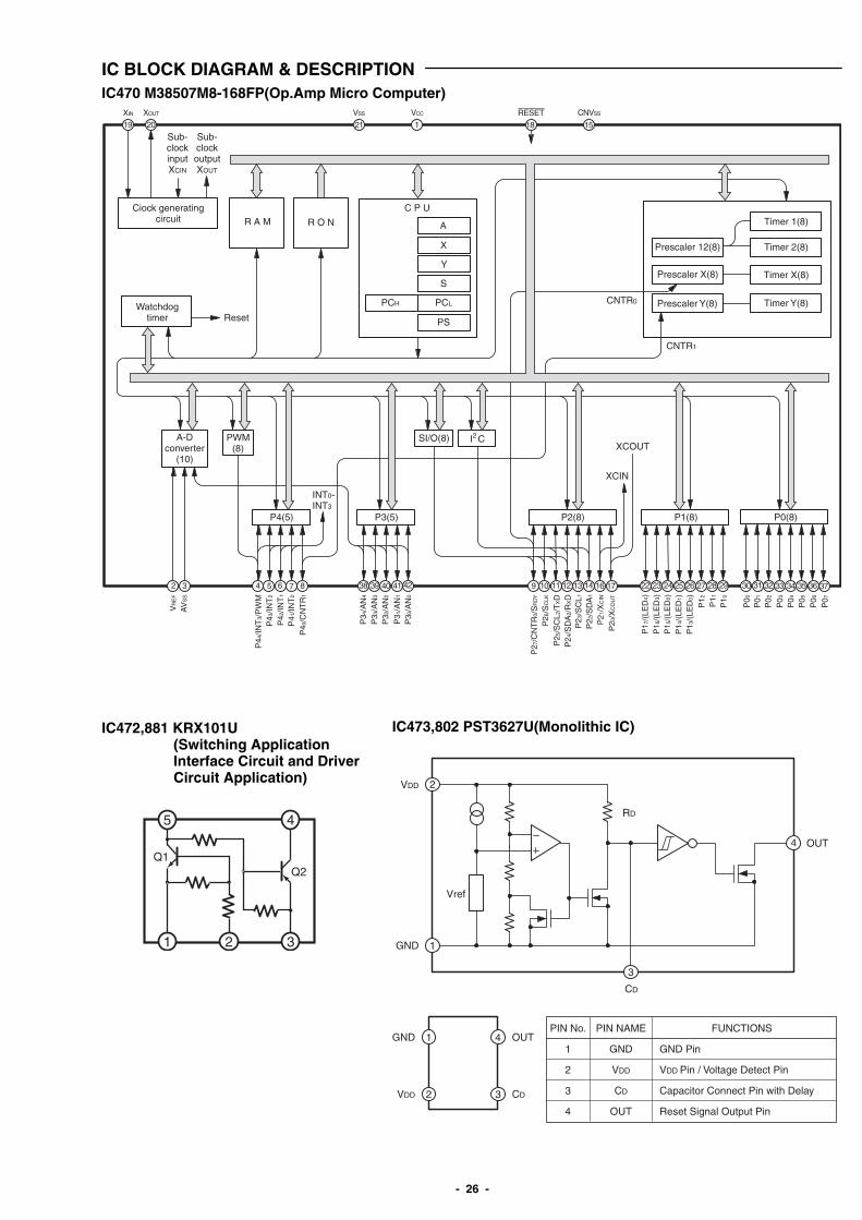
IC472,881 KRX101U(Switching ApplicationInterface Circuit and DriverCircuit Application)
OUT
GND
VDD
CD
2
1
GND 1
VDD
OUT
CD2
4
3
3
4
RD
Vref
PIN No.
1
2
3
4
PIN NAME
GND
VDD
CD
OUT
FUNCTIONS
GND Pin
VDD Pin / Voltage Detect Pin
Capacitor Connect Pin with Delay
Reset Signal Output Pin
IC473,802 PST3627U(Monolithic IC)
Ciock generatingcircuit
Watchdogtimer
R A M R O N
A-Dconverter
(10)
PWM(8)
P4(5) P3(5) P2(8) P1(8) P0(8)
SI/O(8) I C2
Prescaler 12(8)
Prescaler X(8)
Prescaler Y(8)
Timer 1(8)
Timer 2(8)
Timer X(8)
Timer Y(8)
C P U
A
X
Y
S
PCL
PS
PCH
INT0-INT3
Reset
Sub-clockinputXCIN
Sub-clockoutputXOUT
CNTR0
CNTR1
XCOUT
XCIN
18 151212019
2 3 4 5 6 7 8 9 10 11 12 13 14 16 1738 39 40 41 42 22 23 24 25 27 29 30 31 32 33 34 35 36 372826
XIN XOUT VSS VCC CNVSSRESET
P44
/INT
3/P
WM
P43
/INT
2
P42
/INT
1
P41
/INT
0
P40
/CN
TR
1
VR
EF
AV
SS
P27
/CN
TR
0/S
RD
Y
P26
/SC
LK
P25
/SC
L2/T
XD
P24
/SD
A2/
RXD
P2 3
/SC
L1P
22/S
DA
1
P21
/XC
IN
P20
/XC
OU
T
P30
/AN
0
P31
/AN
1
P32
/AN
2
P33
/AN
3
P34
/AN
4
P00
P01
P02
P03
P04
P05
P06
P07
P10
P11
P12
P13
/(LE
D0)
P1 4
/(LE
D1)
P1 5
/(LE
D2)
P16
/(LE
D3)
P17
/(LE
D4)
IC470 M38507M8-168FP(Op.Amp Micro Computer)
- 27 -
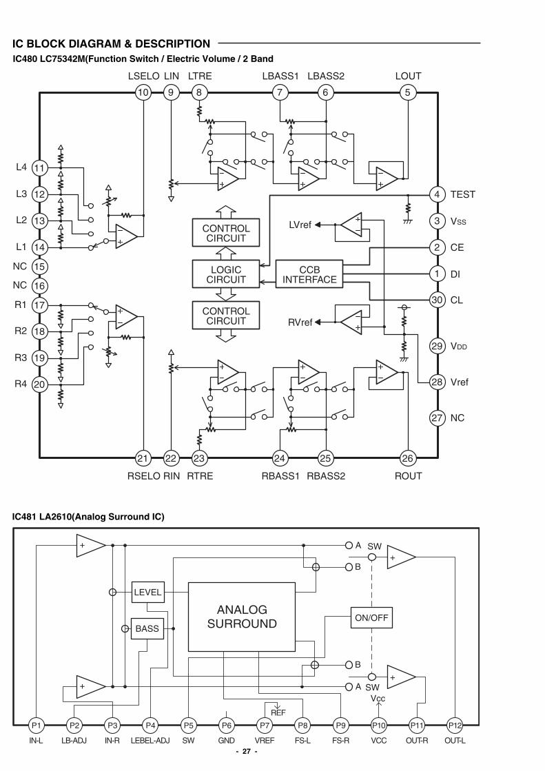
IC BLOCK DIAGRAM & DESCRIPTION
CONTROLCIRCUIT
LOGICCIRCUIT
CCBINTERFACE
CONTROLCIRCUIT
15
14
16
17
18
19
20
21 22 24 25 2623
10 9 7 6 58
11L4
L3
L2
L1
NC
NC
R1
R2
R3
R4
RSELO RIN RTRE RBASS1 RBASS2 ROUT
LSELO LIN LTRE LBASS1 LBASS2 LOUT
TEST
VSS
CE
DI
CL
VDD
Vref
NC
12
13
1
2
30
29
28
27
4
3LVref
RVref
IC480 LC75342M(Function Switch / Electric Volume / 2 Band
P12P10
ANALOGSURROUND
ON/OFF
LEVEL
BASS
A
A
B
B
SW
SW
P1 P2 P3 P4 P5 P6 P7 P8
IN-L IN-RLB-ADJ LEBEL-ADJ GNDSW VREF
REF
FS-L FS-R
P11
VCC OUT-R OUT-L
P9
Vcc
+
++
+
IC481 LA2610(Analog Surround IC)
- 28 -
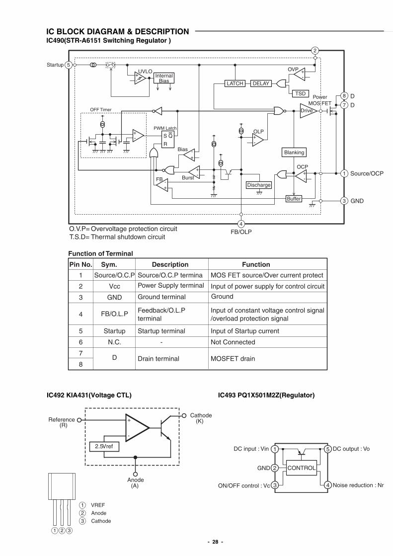
IC492 KIA431(Voltage CTL)
Anode(A)
Cathode(K)Reference
(R)
2.5Vref
+
-
1
1 VREF
2 Anode
3 Cathode
2 3
1 5
3 4
2 CONTROL
DC output : VoDC input : Vin
ON/OFF control : Vc
GND
Noise reduction : Nr
IC493 PQ1X501M2Z(Regulator)
IC BLOCK DIAGRAM & DESCRIPTIONIC490(STR-A6151 Switching Regulator )
5
4
1
3
OVP
TSD
LATCH DELAY
Discharge
Drive
S Q
R
UVLOStartup
InternalBias
Buffer
Blanking
+
+
-
+-
-+-
+-
Burst
+-
Bias -+
OCP
OLP
+-
PWM Latch
OFF Timer
2
Source/OCP
8 D
7 D
GND
FB/OLP
Pin No. Sym. Description Function
Function of Terminal
1
2
3
Source/O.C.P termina
Feedback/O.L.Pterminal
MOS FET source/Over current protect
Input of power supply for control circuit
Input of constant voltage control signal/overload protection signal
Source/O.C.P
Vcc
GND
FB/O.L.P
D
5
6
7
8
4
Power Supply terminal
Startup
N.C.
Startup terminal
-
Drain terminal MOSFET drain
Input of Startup current
Not Connected
Overvoltage protection circuitThermal shutdown circuit
O.V.P=T.S.D=
FB
PowerMOS FET
Ground terminal Ground
- 29 -
IC BLOCK DIAGRAM & DESCRIPTION
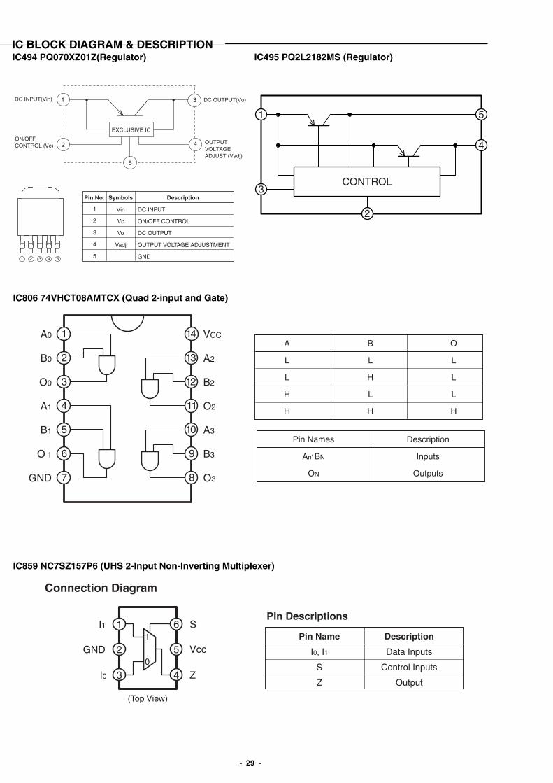
1 2 3 4 5
Description
DC INPUT
ON/OFF CONTROL
DC OUTPUT
OUTPUT VOLTAGE ADJUSTMENT
GND
1
2
3
4
5
Symbols
Vin
Vc
Vo
Vadj
Pin No.
IC494 PQ070XZ01Z(Regulator)
1
2
5
3
4
DC INPUT(Vin)
ON/OFF CONTROL (Vc)
DC OUTPUT(Vo)
OUTPUT VOLTAGE ADJUST (Vadj)
EXCLUSIVE IC
IC495 PQ2L2182MS (Regulator)
3
1 5
4
2
CONTROL
IC806 74VHCT08AMTCX (Quad 2-input and Gate)
1 14A0
2B0
3O0
4A1
5B1
6O 1
7GND
13 A2
12 B2
11 O2
10 A3
9 B3
8 O3
VCCA
L
L
H
H
B
L
H
L
H
Pin Names
An' BN
ON
Description
Inputs
Outputs
O
L
L
L
H
IC859 NC7SZ157P6 (UHS 2-Input Non-Inverting Multiplexer)
I1
GND
I0
1
2
3
6
5
4
S
Z
Vcc
Connection Diagram
(Top View)
1
0
Pin Name
I0, I1
S
Z
Description
Data Inputs
Control Inputs
Output
Pin Descriptions
- 30 -
IC BLOCK DIAGRAM & DESCRIPTION
IC360 NJM2058M (Operational Amplifier)
S1/P1 to S4/P4S5 to S39
COM1COM2COM3COM4
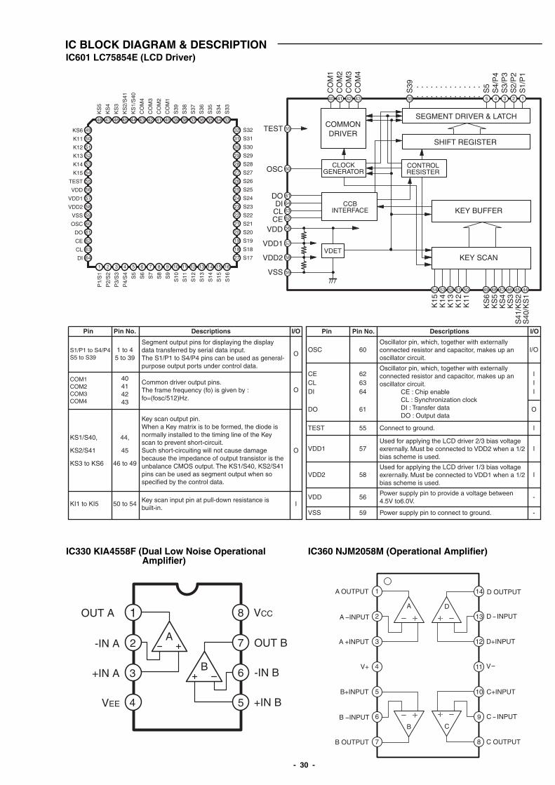
Pin Pin No. Descriptions I/O
1 to 45 to 39
40 41 42 43
O
O
Segment output pins for displaying the displaydata transferred by serial data input.The S1/P1 to S4/P4 pins can be used as general-purpose output ports under control data.
Common driver output pins.The frame frequency (fo) is given by :fo=(fosc/512)Hz.
Key scan output pin.When a Key matrix is to be formed, the diode isnormally installed to the timing line of the Keyscan to prevent short-circuit.Such short-circuiting will not cause damagebecause the impedance of output transistor is theunbalance CMOS output. The KS1/S40, KS2/S41pins can be used as segment output when sospecified by the control data.
KS1/S40,
KS2/S41
KS3 to KS6
44,
45
46 to 49
O
Key scan input pin at pull-down resistance isbuilt-in.
KI1 to KI5 50 to 54 I
49
50
51
52
53
54
55
56
57
58
59
60
61
62
63
64
32
31
30
29
28
27
26
25
24
23
22
21
20
19
18
27
48 47 46 45 44 43 42 41 40 39 38 37 36 35 34 33
1 2 3 4 5 6 7 8 9 10 11 12 13 14 15 16
S32
S31
S30
S29
S28
S27
S26
S25
S24
S23
S22
S21
S20
S19
S18
S17
KS6
K11
K12
K13
K14
K15
TEST
VDD
VDD1
VDD2
VSS
OSC
DO
CE
CL
DI
KS
5
KS
4
KS
3
KS
2/S
41
KS
1/S
40
CO
M4
CO
M3
CO
M2
CO
M1
S39
S38
S37
S36
S35
S34
S33
P1/
S1
P2/
S2
P3/
S3
P4/
S4
S5
S6
S7
S8
S9
S10
S11
S12
S13
S14
S15
S16
56
57
59
58
1234543424140 39
55
61
60
64
63
62
TEST
DODI
OSC
VDD
VDD1
VDD2
VSS
CO
M1
CO
M2
CO
M3
CO
M4
S39
S5
S4/
P4
S3/
P3
S2/
P2
S1/
P1
4445464748495051525354
K15
K14
K13
K12
K11
KS
6K
S5
KS
4K
S3
S41
/KS
2S
40/K
S1
. . . . . . . . . . . . . .
. . . . . . . . . . . . . .
CLCE
COMMONDRIVER
SEGMENT DRIVER & LATCH
SHIFT REGISTER
KEY BUFFER
KEY SCAN
CLOCKGENERATOR
CCBINTERFACE
VDET
CONTROLRESISTER
Pin Pin No. Descriptions I/O
Oscillator pin, which, together with externallyconnected resistor and capacitor, makes up anoscillator circuit.
60OSC I/O
TEST 55 IConnect to ground.
VDD1 57 IUsed for applying the LCD driver 2/3 bias voltageexrernally. Must be connected to VDD2 when a 1/2bias scheme is used.
VDD2 58 IUsed for applying the LCD driver 1/3 bias voltageexrernally. Must be connected to VDD1 when a 1/2bias scheme is used.
VDD 56 -Power supply pin to provide a voltage between4.5V to6.0V.
VSS 59 -Power supply pin to connect to ground.
Oscillator pin, which, together with externallyconnected resistor and capacitor, makes up anoscillator circuit. CE : Chip enable CL : Synchronization clock DI : Transfer data DO : Output data
6263 64
61
CECLDI
DO
III
O
2
3
4 5
6
81OUT A
-IN A
+IN A
VEE
VCC
OUT B
-IN B
+IN B
7
B
A
1
2
3
4 11
12
13
14A OUTPUT
A +INPUT
V+
C+INPUT
A INPUT
B INPUT
D+INPUT
V
D INPUT
D OUTPUT
A D
5
6
7 8
9
10B+INPUT
B OUTPUT
C INPUT
C OUTPUT
B C
IC330 KIA4558F (Dual Low Noise Operational Amplifier)
IC601 LC75854E (LCD Driver)
- 31 -
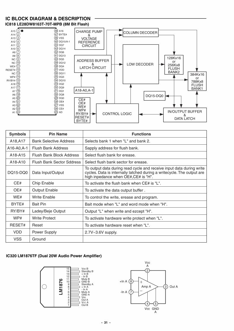
CONTROL LOGIC
CE#OE#WE#WP#
RY/BY#RESET#BYTE#
A18-A0,A-1
ADDRESS BUFFER&
LATCH CIRCUIT
CHARGE PUMP&
VOLTAGEREFERENCE
CIRCUIT
IN/OUTPUT BUFFER&
DATA LATCH
DQ15-DQ0
128Kx16or
256Kx8FLUSHBANK2
384Kx16or
788Kx8FLUSHBANK1
LOW DECODER
COLUMN DECODER123456789101112131415161718192021222324
484746454443424140393837363534333231302928272625
A16BYTE#VSSDQ15/A-1DQ7DQ14DQ6DQ13DQ5DQ12DQ4VDDDQ11DQ3DQ10DQ2DQ9DQ1DQ8DQ0OE#VSSCE#AD
A15A14A13A12A11A10
A9A8NCNC
WE#RESET#
NCWP#
RY/BY#A18A17
A7A6A5A4A3A2A1
Symbols
A18,A17
A16-A0,A-1
A18-A15
A18-A10
DQ15-DQ0
CE#
OE#
WE#
BYTE#
RY/BY#
WP#
RESET#
VDD
VSS
Pin Name
Bank Selective Address
Flush Bank Address
Flush Bank Block Address
Flush Bank Sector Sddress
Data Input/Output
Chip Enable
Output Enable
Write Enable
Bait Pin
Ladey/Beje Output
Write Protect
Reset
Power Supply
Ground
Functions
Selects bank 1 when "L" and bank 2.
Sapply address for flush bank.
Select flush bank for erease.
Select flush bank sector for erease.
To activate the flush bank when CE# is "L".
To activate the data output buffer .
To control the write, erease and program.
Bait mode when "L" and word mode when "H".
Output "L" when write and ezcept "H".
To activate hardware write protect when "L".
To activate hardware reset when "L".
2.7V~3.6V supply.
To output data during read cycle and receive input data during writecycles. Data is internaliy latched during a writecycle. The output arehigh inpedance when OE#,CE# is "H".
IC BLOCK DIAGRAM & DESCRIPTIONIC818 LE28DW8163T-70T-MPB (8M Bit Flash)
IC320 LM1876TF (Dual 20W Audio Power Amplifier)
151413121110987654321
Vcc BStandby B+ In B- In BMute BGND BStandby A+ In A- In AMute AGND AVEEOut AVCC AOut B
LM
1876 8
2
3
+In A
7-In A
Out AAmp A
4
VEE
5
GNDA
VccA
- 32 -
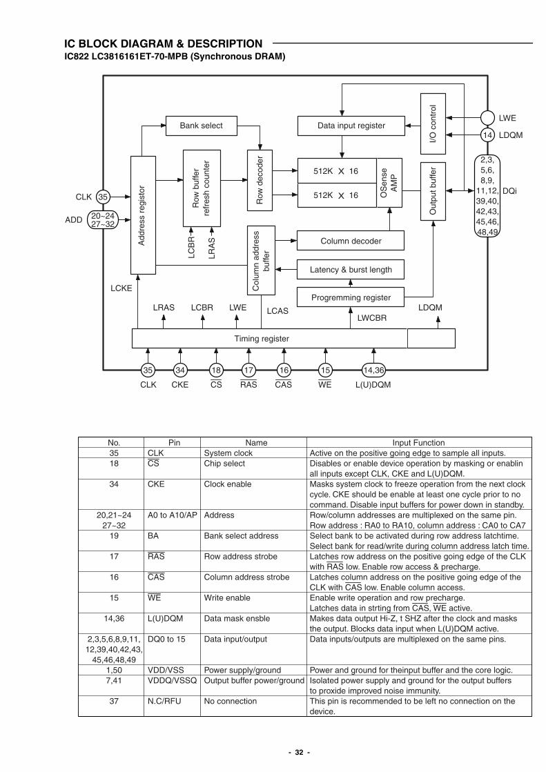
IC BLOCK DIAGRAM & DESCRIPTIONIC822 LC3816161ET-70-MPB (Synchronous DRAM)
Bank select
LRASLWCBR
LCKE
LCBR
LRA
S
LCB
R
LWE LDQM
Add
ress
reg
isto
r
35CLK
LWE
14 LDQM
DQi
35 34 18 17 16
CLK CKE
15
WE
14,36
L(U)DQM
20~2427~32ADD
Data input register
512K 16
512K 16
Column decoder
Latency & burst length
Progremming register
Col
umn
addr
ess
buffe
r
Row
buf
fer
refr
esh
coun
ter
LCAS
Timing register
Row
dec
oder
I/O c
ontr
olO
utpu
t buf
fer
OS
ense
AM
PCASRASCS
No.3518
34
20,21~2427~32
19
17
16
15
14,36
2,3,5,6,8,9,11,12,39,40,42,43,
45,46,48,491,507,41
37
2,3,5,6,8,9,
11,12,39,40,42,43,45,46,48,49
NameSystem clockChip select
Clock enable
Address
Bank select address
Row address strobe
Column address strobe
Write enable
Data mask ensble
Data input/output
Power supply/groundOutput buffer power/ground
No connection
Input FunctionActive on the positive going edge to sample all inputs.Disables or enable device operation by masking or enablinall inputs except CLK, CKE and L(U)DQM.Masks system clock to freeze operation from the next clockcycle. CKE should be enable at least one cycle prior to nocommand. Disable input buffers for power down in standby.Row/column addresses are multiplexed on the same pin.Row address : RA0 to RA10, column address : CA0 to CA7Select bank to be activated during row address latchtime.Select bank for read/write during column address latch time.Latches row address on the positive going edge of the CLKwith RAS low. Enable row access & precharge.Latches column address on the positive going edge of theCLK with CAS low. Enable column access.Enable write operation and row precharge.Latches data in strting from CAS, WE active.Makes data output Hi-Z, t SHZ after the clock and masksthe output. Blocks data input when L(U)DQM active.Data inputs/outputs are multiplexed on the same pins.
Power and ground for theinput buffer and the core logic.Isolated power supply and ground for the output buffersto proxide improved noise immunity.This pin is recommended to be left no connection on thedevice.
PinCLKCS
CKE
A0 to A10/AP
BA
RAS
CAS
WE
L(U)DQM
DQ0 to 15
VDD/VSSVDDQ/VSSQ
N.C/RFU
X
X
- 33 -
IC BLOCK DIAGRAM & DESCRIPTION
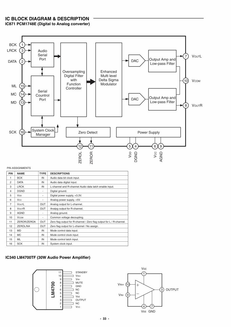
IC340 LM4700TF (30W Audio Power Amplifier)
IC871 PCM1748E (Digital to Analog converter)
VOUTL7
VCOM10
VOUTR8
BCK 1
LRCK 3
DATA 2
ML 15
MC 14
MD 13
SCK 16
ZE
RO
L
12
ZE
RO
R
11
VD
D
5
DG
ND
4
VC
C
6
AG
ND
9
Output Amp andLow-pass Filter
OversamplingDigital Filter
withFunctionController
AudioSerialPort
SerialCountrol
Port
System ClockManager Zero Detect Power Supply
EnhancedMulti level
Delta SigmaModulator
DAC
Output Amp andLow-pass Filter
DAC
1110
987654321
STANDBYVIN+VIN-MUTEGNDNCNCVEE
OUTPUTNCVCC
V
LM
4700
Y
10
1
3
VIN+
9VIN-
OUTPUT
4
VEE
7
GND
Vcc
PIN
1
2
3
4
5
6
7
8
9
10
11
12
13
14
15
16
TYPE
IN
IN
IN
-
-
-
OUT
OUT
-
-
OUT
OUT
IN
IN
IN
IN
NAME
BCK
DATA
LRCK
DGND
VDD
VCC
VOUTL
VOUTR
AGND
VCOM
ZEROR/ZEROA
ZEROL/NA
MD
MC
ML
SCK
DESCRIPTIONS
Audio data bit clock input.
Audio data digital input.
L-channel and R-channel Audio data latch enable input.
Digital ground.
Digital power supply, +3.3V.
Analog power supply, +5V.
Analog output for L-channel.
Analpg output for R-channel.
Analog ground.
Common voltage decoupling.
Zero flag output for R-channel / Zero flag output for L / R-channel.
Zero flag output for L-channel / No assign.
Mode control data input.
Mode control clock input.
Mode control latch input.
System clock input.
PIN ASSIGNMENTS