Embed Size (px)
Citation preview

SERVICE MANUAL Colour Television
SpecificationsPower Source . . . . . . . . . AC220-240V, 50Hz.Colour System . . . . . . . . PAL (AV input: PAL/NTSC4.43/NTSC/PAL-60Hz)Television System . . . . . . B/GChannel Coverage . . . . .Australia
VHF: 0-11, 5AUHF: 28-69CATV: S1-S41, X, Y, Z, Z+1, Z+2
New Zealand VHF: 1-11UHF: 21-69CATV: S1-S41, X, Y, Z, Z+1, Z+2
Video IF . . . . . . . . . . . . . . 38.0MHz Aerial Input Impedance . . 75ΩExt. Terminals
Video inputs: Phono jack 2 (1Vp - p, 75Ω)Audio inputs: Phono jack 2 (436mVrms, more than 40KΩ)Video monitor output: Phono jack 1(1Vp - p, 75Ω)Audio monitor output: Phono jack 1(436mVrms, less than 600Ω)
Sound Output (RMS) . . . . 2 WSpeaker . . . . . . . . . . . . . . 5 cm X 9 cm X 1 pc.Dimensions . . . . . . . . . . . 363 (W) 346 (H) 366 (D)mmWeight . . . . . . . . . . . . . . . approx. 8.6 Kg
Specifications subject to change without notice.
Original Version
Chassis Series: AC5-G
C2CK/C2CM
FILE NO.
Model No. CP14SR1(G)
(Australia/New Zealand)
Give complete “SERVICE REF. NO.” forparts order or servicing. It is shown on therating plate at the cabinet back of the unit.
This T.V. receiver will not work properly in foreign countries where the televisiontransmission system and power source dif-fer from the design specifications. Refer tothe specification table.
0
7
1 4
85
2 3
6
9
P
P
JXMYA
-/--
P P
TV/AV
A B
CH SCAN
TIMER
MENU PIC MODE
SWAP
BASS SURROUND
Service Ref. No.CP14SR1-50CP14SR1(G)-50(Australia)
CP14SR1-60CP14SR1(G)-60(New Zealand)
Product Code: 111355109
REFERENCE NO. SM5110478
- NOTE -The electric specification of the product of allService Ref. No. is completely the same.The difference is as follows:1) Destination CP14SR1-50 & CP14SR1(G)-50
...Australia CP14SR1-60 & CP14SR1(G)-60...New Zealand
2) The difference in a parts list is only a ratedlabel.
CHGAME - +
VIDEO AUDIO

Contents
-2-
Safety Notice . . . . . . . . . . . . . . . . . . . . . . . . . . . . . . . . . . . . . . . . . . . . . . . . . . . . . . . . . . . . . . . . . . . . . . . . 2Chassis Block Diagram . . . . . . . . . . . . . . . . . . . . . . . . . . . . . . . . . . . . . . . . . . . . . . . . . . . . . . . . . . . . . . 3-4IC Block Diagrams . . . . . . . . . . . . . . . . . . . . . . . . . . . . . . . . . . . . . . . . . . . . . . . . . . . . . . . . . . . . . . . . . . 5-7Service Information . . . . . . . . . . . . . . . . . . . . . . . . . . . . . . . . . . . . . . . . . . . . . . . . . . . . . . . . . . . . . . . . . . . 7Service Adjustments with replacing Memory IC (IC802) . . . . . . . . . . . . . . . . . . . . . . . . . . . . . . . . . . . . . 8-11Service Mode Adjustments . . . . . . . . . . . . . . . . . . . . . . . . . . . . . . . . . . . . . . . . . . . . . . . . . . . . . . . . . . 12-13Service Adjustments . . . . . . . . . . . . . . . . . . . . . . . . . . . . . . . . . . . . . . . . . . . . . . . . . . . . . . . . . . . . . . . . . 14Special Function . . . . . . . . . . . . . . . . . . . . . . . . . . . . . . . . . . . . . . . . . . . . . . . . . . . . . . . . . . . . . . . . . . . . .15Purity and Convergence Adjustment . . . . . . . . . . . . . . . . . . . . . . . . . . . . . . . . . . . . . . . . . . . . . . . . . . . . . 16Cabinet Parts List . . . . . . . . . . . . . . . . . . . . . . . . . . . . . . . . . . . . . . . . . . . . . . . . . . . . . . . . . . . . . . . . . . . 17Chassis Electrical Parts List . . . . . . . . . . . . . . . . . . . . . . . . . . . . . . . . . . . . . . . . . . . . . . . . . . . . . . . . . 18-23
Safety Notice
SAFETY PRECAUTIONS
1: An isolation transformer should be connected in thepower line between the receiver and the AC linewhen a service is performed on the primary of theconverter transformer of the set.
2: Comply with all caution and safety-related notes pro-vided on the cabinet back, inside the cabinet, on thechassis or the picture tube.
3: When replacing a chassis in the cabinet, always becertain that all the protective devices are installedproperly, such as, control knobs, adjustment coversor shields, barriers, isolation resistor-capacitor net-works etc.. Before returning any television to thecustomer, the service technician must be sure thatit is completely safe to operate without danger ofelectrical shock.
X-RADIATION PRECAUTION
The primary source of X-RADIATION in television receiver is the picture tube. The picture tube is specially con-structed to limit X-RADIATION emissions. For continued X-RADIATION protection, the replacement tube must bethe same type as the original including suffix letter. Excessive high voltage may produce potentially hazardous X- RADIATION. To avoid such hazards, the high voltage must be maintained within specified limit. Refer to this ser-vice manual, high voltage adjustment for specific high voltage limit. If high voltage exceeds specified limits, takenecessary corrective action. Carefully follow the instructions for + B1 volt power supply adjustment, and high volt-age check to maintain the high voltage within the specified limits.
PRODUCT SAFETY NOTICE
Product safety should be considered when a component replacement is made in any area of a receiver.Components indicated by mark in the parts list and the schematic diagram designate components in whichsafety can be of special significance. It is particularly recommended that only parts designated on the parts listin this manual be used for component replacement designated by mark . No deviations from resistancewattage or voltage ratings may be made for replacement items designated by mark .

-3-
Chassis Block Diagrams
Fron
tke
y
A19
01A
RC
PR
E-A
MP.
D19
10LE
D
5V-2
67
AN
T
VID
EO
IN
AUD
IO-IN
AU
DIO
MO
NIT
OR
OU
T
FR
ON
TA
V IN
RE
AR
AV
IN
VID
EO IN
IC80
2M
EM
OR
Y6
5
43
SC
LS
DA
Key
in
R/C
in
3129
Sta
nd b
yMut
eP
rote
ct
2710
8
AFT
BLKBGR
36V
9 11IF
OU
T
CP
U
1V
IFR
F A
GC
A10
1T
UN
ER
X16
1S
AW
Filt
er
15V
40
SELECTED VIDEO OUT
15142
AUD
IO-O
UT
Ext
.AU
DIO
-IN
Ext
.VID
EO
-IN
RF
AG
C
AF
C
AB
L
28
13
4
IF in
IF in
6
AF
T
SIF
ou
t
SIF
in
IF VC
C
VIDE
OVE
RT
V CC
RG
BV
CC
HO
R.
VC
C
5V-2
10
52
54
8 43
5
18
25
H-V
CC
9V
9V-1
85V
RC
14
15
16
17
R G B BLK
46 44 35
34
VID
EO
-OU
T
INT.
VID
EO
IN
R-Y
IN
9V-1
B-Y
IN
R-O
UT
G-O
UT
B-O
UT
H-O
UT
V-O
UT
19 20 21 27 23
IC20
1IF
/VID
EO
/C
HR
OM
A
MU
TE
AU
DIO
-IN
AU
DIO
O
UT
IC00
1AU
DIO
AM
P.(M
ONO
)
IC28
1S
EC
AM
6 7
Low
B
5V-2
TE
LE
TE
XT
UN
IT
TEXT: RTEXT: GTEXT: B
TEXT: BLK
180V
VIDEO IN
14
SE
CA
M K
ILLE
R
15
IC50
1V
ER
T./D
EF.
SW
ITC
HV
R63
113
0VR
eg.
Reg
.24
V
15V
9V
5VR
CR
eg.
Reg
.
24V
Pro
tect
T43
1H
-DR
IVE
TR
AN
S.
Q43
2H
-OU
T
25V
130V
BGR
9V
H V
L902
DY
AF
CA
BL
T47
1F
BT
Q90
1C
RT
Hea
ter
HV
180V
Hea
ter
Low
B
36V
H-V
CC
9V-1
5V-2
Pro
tect
PO
WE
R S
UP
PLY
CIR
CU
IT
Pro
tect
4/5
IC80
112 28
19 20 21 22
SP
901
7539
RE
AR
MO
NIT
OR
OU
TV
IDE
O M
ON
ITO
R O
UT
AUD
IO-IN
11/1
2
2
Q43
1H
-DR
IVE
1315IC20
01T
ELE
TE
XT
DE
CO
DE
R
89
1012
16/1
71
CR
T U
NIT
T61
1C
ON
VE
RT
ER
TR
AN
S.
2
AUDIO MONITOR OUT
IIC B
us
IIC B
us
IIC B
us
IIC B
us
1 / 2
MAIN SIGNAL PROCESSING CIRCUIT
Teletext decoder and SECAM decoder are not equipped.

-4-
Chassis Block DiagramsSYSTEM CONTROL
12K
EY
SW
ITC
H IN
KE
YS
WIT
CH
SC
L2 1 31
SD
A
PO
WE
R O
N/O
FF
PH
OT
O C
OU
PLE
(O
N=
HIG
H, O
FF
=LO
W)
IC20
1IF
/VID
EO
/ C
HR
OM
A/D
EF
.
IC80
1C
PU
QX
XA
BV
864
22 19 20 21 18 17 273
4763228
OS
D B
LK O
UT
(Act
ive=
Hig
h)
OS
D R
ED
OU
T(A
ctiv
e=H
igh)
OS
D G
RE
EN
OU
T(A
ctiv
e=H
igh)
OS
D B
LUE
OU
T(A
ctiv
e=H
igh)
DE
FLE
CT
ION
CIR
CU
IT
HO
RIZ
. SY
NC
IN (
AC
TIV
E=
LOW
)
VE
RT
. SY
NC
IN (
AC
TIV
E=
LOW
)
PO
WE
R P
RO
TE
CT
IN
(P
OW
ER
ER
RO
R=
LOW
)P
OW
ER
CIR
CU
ITet
c.
SCL
SDA
IC80
2M
EM
OR
Y
OS
CX
801
32.7
68K
Hz
CP
U O
SC
OU
T
CP
U O
SC
IN
LED
ON
-TIM
ER
LE
D O
UT
(ON
TIM
ER
ON
=Lo
w)
RC
SIG
NA
L IN
(AC
TIV
E=
HIG
H)
RC
PR
E-A
MP
.
IC00
1A
UD
IO A
MP
.(M
ON
O)
A10
1F
/S T
UN
ER
AF
T S
IGN
AL
INP
UT
10
RE
SE
T IN
PU
T (
AC
TIV
E=
LOW
)13
MU
TE
OU
TP
UT
(MU
TE
ON
=H
IGH
)29
56
3

-5-
IC Block DiagramsIC201 < IF/Video/Chroma/Def. > LA76818A
1
DC
VO
L
SW F
MD
ET
23
45
6
IFA
GC
RF
AG
C
VIF
78
910
IFV
CC
5V11
1213
BU
S
PE
AK
ING
CO
RIN
GB
LAC
KS
TR
ET
CH
SY
NC
SE
P
1415
AB
L
DC
RE
ST
CLA
MP
OS
DC
ON
TR
AS
TB
RIG
HT
1617
1819
20
CO
NT
RA
ST
BR
IGH
TR
GB
MAT
RIX
OS
DS
W
DR
IVE
/OU
T-OF
F
VC
C21
2223
FS
C/
SY
NC
SW
2425
2627
VE
RR
AM
PH
OR
VC
CHV
CC
VE
RC
/D
HO
RO
UT
PH
AS
ES
HIF
TE
R
AF
C2
AF
C1
VE
RS
EP
HO
RC
/D
1/256
CO
LOR
CLA
MP
LPF
ALC
+S
WC
LAM
P
DE
MO
PAL
SW
AC
C
BP
FO
N/O
FF
DE
LAYLIN
E
SW
TR
AP
AF
TV
IDE
OD
ET
TR
AP
LIMA
MP
BP
F
SP
LL
BP
F
VID
EO
AM
P
IFID
EN
TV
IDE
O
SW
AP
C1
TIN
T
VX
OD
DS
AP
C2
DC
AD
S.
CLA
MP
VC
O
1H D
ELAY
HO
RV
CO
FB
P
2829
3031
321H
VC
C
3334
3536
3738
3940
4142
CLM
P
4344
45
CLM
P
V/C
VC
C5V
4647
4849
50
A2C
PLL
5152
5354Audio Output
FM Output/Selected Audio Output
PIF AGC
RF AGC Output
PIF Input1
PIF Input 2
IF Ground
IF Vcc
FM Filter
AFT Output
Bus Data
Bus Clock
ABL
Red Input
Green Input
Blue Input
Fast Blanking Input
RGB Vcc
Red Output
Green Output
Blue Output
fsc output or CSync output
Vertical Output
Ramp ALC Filter
Horizontal/BUS Vcc
Horizontal Output
Horizontal AFC Filter
Flyback Pulse Input
VCO IREF
Clock (4MHz) Outupt
CCD Vcc
CCD Filter
CCD/Horizontal Ground
SECAM B-Y Input (Cb Input)
SECAM R-Y Input (Cr Input)
Chroma APC2 Filter
Clamp Filter
4.43 MHz Crystal
Chroma APC1 Filter
Selected Video Output
Video/Vertical/BUS Ground
External Video Input(Y-IN)
Video/Vertical Vcc
Internal Video Input (S-C IN)
Black Level Detector
Video Output
VCO Filter
VCO Coil 2
VCO Coil 1
APC Filter
Ext. Audio Input
SIF Output
SIF APC Filter
SIF Input

IC Block Diagrams
-6-
IC201 <IF System Block Diagram> LA76818A
1112
BU
SIn
terf
ace
SA
W
5 6 4 8 7
PIF
In1
PIF
In2
IF In
9V
30K
RF
AG
CO
ut
120K
IF V
CC
IFG
ND
VIF
AM
P
VIF
1V
IF 2
VIF
3
IF A
GC
D
rive
RF
AG
C2n
dIF
AG
C
RF
AG
CD
elay
6bit
IF A
GC
Def
1bit
+ - (6 V
cc)/
7
To BU
S
3
0.02
2uP
IFA
GCIF
AG
C
Dat
aC
lock
AP
CD
et
+π/
4
-π/4
Snd Det
Am
p
52S
IF.O
ut
Sou
ndTr
ap
Vid
eoD
et
Buz
zC
ance
ller
50A
PC
Filt
er33
00.
47u
+
PLL
Pul
l-in
SW
To BU
S
Lock
Det
Vid
eo.L
evel
3b
it
Am
p54
10p
SIF
.In
Sou
ndB
PF
VC
O.C
oil
VC
OC
OIL
1V
CO
CO
IL2
4849
VIF
VC
OC
hrom
aC
ount
er
B/N
INV
IFId
ent
OS
CC
/D
Am
p
SIF
. Sys
2bit
pre-
scal
ler
SIF
VC
O
500K
BP
FSIF
AP
CF
ilter
1K
0.01
u10
00p
53LI
MA
MP
FM
Det
FM
.Lev
el5b
it
Chr
oma
C/D
AP
CD
et
500K
Det
To BU
S
Chr
oma
VC
O VIF
Cou
nter
Res
etP
ulse
VC
OId
ent
VIF
.Sys
2bit
Pha
seD
etec
tor
A.M
UT
E1b
itV
OLU
ME
D/A
VO
LUM
EF
ilter
A.S
W1b
itInpu
tS
elec
tV
OLU
ME
(AT
T)
-+
-+
2.5V
Am
p
FM
Gai
n1b
itD
eem
-TC
1bit
De-
emph
FM
Mut
e1
bit
2 9 46 51 1
A.F
il.D
ef1b
it
VO
LUM
E7b
it
47
VC
OA
lignm
ent
AF
T10
AF
T
Vcc 100K 100K
0.1u
VC
OF
ilter
+
0.47uAud
io.o
ut
+Aud
io in
10u
Vid
eo
Out
FM
Filt
er+
1u
FM
Out
0.01u
+
to B
US
Lin
e
+

-7-
IC Block Diagrams
IC501 < Vertical Output > LA78040/LA78040N
ThermalProtection
-
+AMP
PumpUp
1
INV
ER
TIN
G
INP
UT
2
Vcc
3
PU
MP
UP
OU
T
4
GN
D
5
Ver
. OU
TP
UT
6
OU
TP
UT
S
TAG
E V
cc
7
NO
N IN
V.IN
PU
T
IC001 < Audio AMP.> LA4266
1 2 3 4 5 6 7 8 9 10NC NC Filter PRE
GNDIN2
300Ω 30kΩ
NF2 OUT2 PowerGND
VCC NC
Service Information
This TV set has a built-in power supply protection circuit.It is provided to protect the TV set in case of a power supply circuit malfunctions. When something abnormalityoccurs during TV reception, the TV set goes to the stand-by mode.
When an abnormality occurs during TV reception, it causes pin 27 of the CPU to go continually Low(less than0.75V) for about one second. The CPU detects that this has occurred and outputs the signal from pin 31 toswitch off the power supply lines.
Releasing the protective circuit and restoring power supply
To release the protective circuit and restore power supply, turn the power to the TV set OFF and then ON againvia either the main power switch or the ON-OFF button on the remote control. This will work only if the powersupply trouble was temporary. If there is permanent trouble such as a damaged circuit, power cannot berestored and the circuit will have to be repaired.
Protection Circuit

[1] Initializing Procedure1. Put a new memory IC.2. Turn on the TV set.3. Press and hold the GAME button on the TV set for more than 2 seconds. The following picture appears on the
screen.
4. Press the PROGRAMME UP on the TV set while the above On-Screen Display is still on the screen. The followingpicture appears on the screen.
This completes the initialization of memory IC.
Following shows the initialized contents of memory data by this procedure.- Plug & Play : No executed- Inhibit Data : Cancelled- Ch Skip Data : Cancelled- Sound Volume Data : 10/63 steps.- Volume Lock : OFF- Tuning Lock : OFF- Music Mode : OFF- AV Start : OFF- Colour System : AUTO
1
CLR
CHGAME - +
-8-
Service Adjustments with Replacing Memory IC(IC802)
Note: The CPU (IC801) and memory IC (IC802) store the service adjustments data and controls data for each circuit.When the Memory IC(IC802) is replaced, some of the service adjustments should be readjusted to obtain the best performance. The necessary service adjustments are carried out by using the RC handset.Please set up the TV set with following steps [1] to [2].
Press and hold for more than 2 seconds
CHGAME - +
GAME
PROGRAMME UP
[2] Required Service AdjustmentsReadjust the following service adjustments.Adjustments Service Mode No. & ItemRF AGC Item 01, RF AGCHorizontal centre Item 02, H-PHAVertical size Item 04, V-SIZVertical-S correction Item 05, V-SCOVertical linearity Item 06, V-LINGray scale Item 14-17, 19-21
Further adjustment please refer to page 12 and 13.

-9-
Service Adjustments with Replacing Memory IC(IC802)
NO. ITEMDATA
RANGEINITIALSETUPDATA
DESCRIPTION
01020304050607080910
11
12
1314151617181920
RF AGC Adj.RF AGC 00~63 35H-Phase (H-Centering) Adj. (50Hz)H-PHA 00~31 3V-Position (V-Centering) Adj. (50Hz) Fixed.V-POS 00~63 40V-Size Adj. (50Hz)V-SIZ 00~127 75V-S Correction (50Hz)V-SCO 00~31 11V-Linearity Adj. (50Hz)V-LIN 00~31 18H-Centering Adj. (60Hz) H-P60 -16~+15 +5V-Size Adj. (60Hz) V-S60 -64~+32 0OSD H-Position Adj.OSDHP 00~255 30OSD Contrast Adj.OSDC 00~127 50Correction of the V-size accompanying brightness change. V-SCP 00~07 7
Correction of the H-size accompanying brightness change.H-SCP 00~07 7
Sub Bias Adj.SBIAS 00~127 105
Red Bias Adj.RBIAS 00~255 0Green Bias Adj.GBIAS 00~255 0Blue Bias Adj.BBIAS 00~255 0Red Drive Adj.RDRIV 00~127 64Green Drive Adj.GDRIV 00~15 8Blue Drive Adj.BDRIV 00~127 64
1-LINE APPEAR
21 DRV White Balance Adj.22 B-YD 00~15 8 B-Y DC level Adj.. Colour compensation (PAL)
23 R-YD 00~15 8 R-Y DC level Adj.. Colour compensation (PAL)
24 B-YDN -16~+15 0NTSC B-Y DC level Adj. (Difference value over PAL.)
25 R-YDN 0NTSC R-Y DC level Adj. (Difference value over PAL.)
26 SBDC -8SECAM B-Y DC level Adj. (Difference value over PAL.)
27 SRDC -5SECAM R-Y DC level Adj. (Difference value over PAL.)
28 G-YA 0,1 0G-Y angle Adj. (The reproducibility of a colour is changed.)
29 RBGB 00~15 8 R-Y, B-Y Gain Blance Adj. (Do not change.)30 RBAG 00~15 8 R-Y, B-Y Angle Adj. (Do not change.)
31 G-YAN 0,1 0NTSC G-Y Angle Adj. (Difference value over PAL.)
32 RBGBN 0NTSC R-Y, B-Y Gain Balance Adj. (Difference value over PAL.)
33 RBAGN 0NTSC G-Y, B-Y Angle Adj. (Difference value over PAL)
34 COGV 00~03 0 Coring Adj.35 BLKS 00~03 3 Setting of Black stretch start.36 BLKG 00~03 3 Setting of Black stretch gain.37 BRTA 0,1 0 On and off of ABL.
38 BRST 0,1 0 Setting of ABL.39 BRTH 00~07 0 Setting of ABL.
(Do not change)
4041
42
43
White peak limitter.WPL 00~03 3Y Gamma setting.YGAM 00~03 0Switching of Pre-shoot and Over shoot in AV mode.PORW 0,1 0
Pre-shoot/Over shoot Adj. in AV mode.PORS 00~03 2
-16~+15
-16~+15
-16~+15
-16~+15
-16~+15
NO. ITEMDATA
RANGEINITIALSETUPDATA
DESCRIPTION
444546474849505152535455
5657
58
59
60
636465
RF Coring Gain Adj.RFCO 00~03 0Switching of RF Pre-shoot and Over shoot. PORWN 0,1 0RF Pre-shoot/Over shoot Adj. PORSN 00~03 0RF Tint Adj.TINT -16~+15 0NTSC 4.43 Tint Adj.TINT 443 -16~+15 -12RF Sharpness Adj.SHRF -32~+31 0OSD TEXT Contrast.TEXTC -128~+127 0
VOLUM 127001
16
0,1
0
1
00~2551
3400~63136
0,1 0
00~07
6667
0
68
0
69
0
701
710
720
731
74375
64
76
0
77
0
78
5
79
0
80
0
81
82
183
112
84
6492
245
3
0
Volume Control Adj.00~255De emphasis TC.DEEM 00~01VIF System Switch.VIFSW 00~03SIF System Switch.SIFSW 00~03
Video Level Adj.V-LVL 00~07 4FM Level Adj.FMLVL 00~31IF TestIF-TE 0,1
IF Test-1IF-T1
IF-T2
IF-T3
61 H-FRQ Correction of Horizontal Frequency.62 FBTS Switching of H-blanking and Flyback Pulse.
COOP00~07
Setting of Colour Killer Level.HBLKL H-Blanking Control. (Left)HBLKR 00~07 H-Blanking Control. (Right)AFCRF 0,1 RF AFC Gain & Gate Adj.VSURF 0,1 RF V-Sync. Separation Adj.
CDMRF 00~07 RF V-Countdown Circuit Adj.AFCAV 0,1 AV AFC Gain & Gate Adj.VSUAV 0,1 AV V-Sync. Separation Adj.CDMAV 00~07 AV V-Countdown Circuit Adj.HLVDRF 0,1 H Lock, V Detect RF modeHLVDAV 0,1
VCO-SW 0,1 C-VCO Adj. Switch.VCO-ADJ 00~03 C-VCO Adj.
CROSS-BW 00~03 Pattern Output.AVNCON 00~127 Contrast Adj. of the blue back in AV mode.
AVNBRI 00~127 Brightness Adj. of the blue back in AV mode.
IF Test-2
POMT 00~127 Power Mute Time Adj.
CHMT 00~31 Channel Change Mute time Agj.
SYST 00~15Selection of the number of times of a Colour system judgment.
S-STE 0,1Stereo/Mono Option. 0=MONO, 1=AV STEREO
VOLTBLSelection of the change characteristic of volume.
818/828 Metal Option
302 R02 00~255 CPU Debug Date.303 R03 00~255 CPU Debug Date.
301 R01 00~255 CPU Debug Date.
300 R00 00~255 CPU Debug Date.
CHIP818
0,1IF Test-3
7
73
1 H Lock, V Detect AV mode
6425
10
CPU Debug Date.
CPU Debug Date.
CPU Debug Date.0
00~255
00~255
00~255
304
305
306
R04
R05
R06
0~3
0,1
Following table shows the initial values which have been stored in the CPU ROM, and items for the service adjustments.
Service mode adjustments table in CPU ROM

-10-
Service Adjustments with Replacing Memory IC(IC802)
Notes: The initial value that the CPU writes down the CPU ROM data to the memory when replaced the memory IC.TV set may not operate correctly with this initial value. It is required to set up the fine adjustment for service adjustments described in the above.
NO. ITEMDATA
RANGEINITIALSETUPDATA
DESCRIPTION
307308309310311312313314315316317
320321322323324325326327328
032
112237159
110
219223249221
15
33
112
8033
112
96000329
330 0331 0332 0
3340000
335
0336
0337
0225
3
338
144
340
3
341
33
342
248339325
345 92
347
0
348
0
349
0
350
0
351
0
352
0
353354
355356357358
359
0
000
R09
R10
R08R07 00~255
00~25500~25500~25500~25500~25500~25500~25500~25500~25500~25500~25500~25500~25500~25500~25500~25500~25500~25500~25500~25500~25500~25500~25500~25500~25500~25500~25500~25500~25500~25500~25500~25500~25500~25500~25500~25500~25500~25500~25500~25500~25500~25500~25500~25500~25500~25500~25500~25500~25500~25500~25500~255
CPU Debug Date.CPU Debug Date.CPU Debug Date.CPU Debug Date.CPU Debug Date.CPU Debug Date.CPU Debug Date.CPU Debug Date.CPU Debug Date.CPU Debug Date.CPU Debug Date.CPU Debug Date.CPU Debug Date.CPU Debug Date.CPU Debug Date.CPU Debug Date.CPU Debug Date.CPU Debug Date.CPU Debug Date.CPU Debug Date.CPU Debug Date.CPU Debug Date.CPU Debug Date.CPU Debug Date.CPU Debug Date.CPU Debug Date.CPU Debug Date.CPU Debug Date.CPU Debug Date.CPU Debug Date.CPU Debug Date.CPU Debug Date.CPU Debug Date.CPU Debug Date.CPU Debug Date.CPU Debug Date.CPU Debug Date.CPU Debug Date.CPU Debug Date.CPU Debug Date.CPU Debug Date.CPU Debug Date.CPU Debug Date.CPU Debug Date.CPU Debug Date.CPU Debug Date.CPU Debug Date.CPU Debug Date.CPU Debug Date.CPU Debug Date.CPU Debug Date.CPU Debug Date.CPU Debug Date.
R11R12
R13R14R15R16R17R18R19R20R21R22R23R24R25R26R27R28R29R30R31R32R33R34R35R36R37R38R39R40R41R42R43R44R45R46R47R48R49R50R51R52R53R54R55R56R57R58R59
318319
333
339
343344
346
NO. ITEMDATA
RANGEINITIALSETUPDATA
DESCRIPTION
360361362363364365
368369370371372
000000000
0
00~25500~25500~25500~25500~25500~25500~25500~25500~255
00~25500~255
00~25500~255
0132
0
366367
R60R61R62R63R64R65R66R67R68R69R70R71R72
CPU Debug Date.CPU Debug Date.CPU Debug Date.CPU Debug Date.CPU Debug Date.CPU Debug Date.CPU Debug Date.CPU Debug Date.CPU Debug Date.CPU Debug Date.CPU Debug Date.CPU Debug Date.CPU Debug Date.
34114

-11-
TIMER
P
P
ADDRESSDRV
SI. 00100101S2.11111000DATA
B 6421 R 64ADDRESS
V-SCO
SI. 00100101S2.11111000DATA
905
ADDRESSRF AGC
SI. 00100101S2.11111000DATA
3001
Service Adjustments with Replacing Memory IC(IC802)
[Entering to Service Mode]
1. Press and hold the MENU button on the Remote Control and press the VOLUME (+) button on the TV set.Following setting items appears on the screen.
Display for [V-SCO] V-S Correction adjustment
Read Status
Item No. Item Data value
Display for [RF AGC] RF AGC adjustment
Read Status
Item No. Item Data value
Data value for Red
Display for [DRV] White balance adjustment
Read Status
Item No. Item
Data value for Blue
To return to normal TV mode, press the MENU button on the TV set or the remote control handset.
2. Select item by pressing the TIMER (Item No. UP) or SOUND MUTE (Item No. DOWN) button on the remote controlhandset.
3. Adjust data value by pressing the VOLUME + or VOLUME - button on the remote control handset.
Example
MENU
MENU
CHGAME - +
0102030405......84... ...8483828180......01

-12-
Service Mode AdjustmentsFollowing adjustments should be carried out when the memory IC is replaced. How to enter the service mode andadjust values, please refer to “ Entering to Service mode” on page 11.
Vertical size
NOTE: Do not attempt this adjustment with weak signal.(1) Tune the receiver to most clearest (or strongest) VHF
station in your area. Set the brightness and contrastcontrols to maximum. Set the colour control to minimum.
(2) Select [RF AGC] in the service mode.(3) Change value until the snow noise just disappears.(4) Exit from service mode.
Item 01 [RF AGC] AGC
(1) Receive a monochrome circular pattern.(2) Set the brightness and contrast to normal.(3) Select [H-PHA] in the service mode.(4) Change value to be optimum horizontal centre position.(5) Exit from service mode.
Item 02 [H-PHA] HORIZONTAL CENTRE
Horizontal centre
(1) Receive a monochrome circular pattern.(2) Set the brightness and contrast to maximum.(3) Select [V-SIZ] in the service mode.(4) Change value to be optimum vertical size.(5) Exit from service mode.
Item 04 [V-SIZ] VERTICAL SIZE
(1) Receive a crosshatch pattern.(2) Set the lever of SW501 (Vertical Center SW) as the
position of a center.(3) Select a picture mode of NATURAL by pressing the
PICTURE MODE button.(4) Select [V-SCO] in the service mode.(5) Adjust Vertical S-letter Correction so that the difference
of “c”, “d” and “e” becomes less than 2 mm by pressingthe VOLUME + or - button.
(6) Confirm Vertical Linearity and adjust Vertical Center then Vertical Size.
(7) Exit from service mode.
Item 05 [V-SCO] V-S CORRECTION
c Upper
Center
Bottom
d
e
(1) Receive a crosshatch pattern.(2) Set the lever of SW501 (Vertical Center SW) as the
position of a center.(3) Select a picture mode of NATURAL by pressing the
PICTURE MODE button.(4) Select [V-LIN] in the service mode.(5) Adjust Vertical Linearity so that the difference of “a” and
“b” becomes less than 3mm by pressing VOLUME + or- button.
(6) Exit from service mode.
Item 06 [V-LIN] VERTICAL LINEARITY
a
b
Upper
Center
Bottom

-13-
0
7
1 4
85
2 3
6
9
P
P
JXMYA
-/--
P P
TV/AV
A B
CH SCAN
TIMER
MENU PIC MODE
SWAP
BASS SURROUND
(1) Receive the monochrome circular pattern.(2) Set the brightness and colour to normal, contrast to maximum.(3) Enter to the service mode.(4) Set each value of Item-14 RBIAS, 15 GBIAS, 16 BBIAS, 17 RDRIV and 19 BDRIV mode to 64.(5) Select Item-20 mode to be one horizontal scanning line and turn the screen volume on the FBT to obtain just visible
one coloured line.(6) Press the 1 (Red Bias -), 2 (Red Bias +), 5 (Green Bias -), 6 (Green Bias +), 9 (Blue Bias -) or 0 (Blue Bias +)
button to adjust the brightness of each colour until a dim white line produced. Please see the control button alloca-tions in this mode.
(7) Select Item-21 DRV mode to enter the white balance adjusting mode.(8) Press the 3 (Red Drive -), 4 (Red Drive +), -/-- (Blue Drive -) or RECALL (Blue Drive +) button alternately to
produce normal black and white picture.(9) Exit from the service mode.(10) Check for proper grey scale tracking at all brightness levels.
NOTE: If the grey scale adjustment is made after picture tube replacement, check the high voltage.
Items 14-17, 19-21 GREY SCALE
Service Mode Adjustments
Red Bias -
Red Bias +
Green Bias -
Blue Bias +
Red Drive +
Blue Drive -
Blue Drive +Green Bias +
Blue Bias -
Red Drive -
Press the MENUbutton to exitfrom servicemode.
JP646
JP645
6
D432 KDY-4
KDY-3
KDY-1
T471AT471
T471-H4
T471-H7
T471-H12
T471-H10
T471-H1T471-H2
L441
T471-H11
R477
D485
R488
R424
C471
L631
R48
R355
1
R486
R485
L441
L441A
L441-H3
C437C435-H2
C435-H1
C435-H4
T471FBT
MAIN BOARD
SCREEN VR(Under side)

JP646
JP645
R1001
C107
J1001
R445
K1002
K1001
6
JP442
Q432
T431A
J104
D102
J114
TP-MTP-A
D432 KDY-4
KDY-3
KDY-1
T471AT471
T471-H4
T471-H7
T471-H12
T471-H10
T471-H1T471-H2
L441-H2
L441-H1
T471-H11
1
J033
J103R477 J
05431
J032
R228
D468
C469
D485
R488
R424
C471
L631
R481
5
Q432-H4
Q432-H5
Q432-H3
Q432-H2
R479
C491
C486
Q432-H1
R423
KQ
R426
R475
D467L431
L432
D421
R355
C106
C101
R105
R103
D103
J004JP437
78
R501
R422
OUTIN31
R1006
J106
C132
X171
J105
06
R486
R485
JW6
D476
VID AUDAUDVID
AUDC1004
R1007
C1003
C1001
C1002
J1002
R1003
R1002
D448C449
L441
L441A
L441-H3
C435C435B
R441
R435
C437
C435AC435-H3
C435-H2C435-H1
C441BC441A
C441
D441
C435-H4
C441-H1C441-H2
C441-H3
C441-H4
R435A-H1
R435A-H2
J435C436
C436A
JP436
JP1004
C407
JP1005
J438
T471FBT
T431H-DRIVETRANS.
H-OUT
E
E
E
EE
16
10
71
17 10
16
34
21
KG
AC250V 4A
F601
IC501
R662-H1
R662-H2
R662
C644
IC501-
R518
R519
C520
C518
R512
D512
J
R525
D683
R687
R686
Q683
R663
C662Q
661A
D634
C634
J401
D682
C517
J513
R243
R510
R511
J504
J502
J506
R872
J0
J808
R642
J687
J2
J688
R664-H2
R664-H1
JW3
JP502
J503
JP683
JP633
JP661
JP646
JP645
R646
JP442
D507
J507
D432
C482
J505
KDY-6
KDY-5
KDY-4
KDY-3
KDY-1
T471A
T471-H1T471-H2
L441-H2
L441-H1
R431
R477
C433
Q431
C515
C514
C524
C432J032
L631
J509
R516
R515R514
IC501-H
R355
JP501
T611-H16
JW4 C641
J633
D631 C631JP631
D633
C633
C643
R638
R639
D686R637
R635
VR631
D685
C685
1AA4B10S0160A
R433
J641
J642C521
R645
J645T611-H4
R616R615
R606
R620
R609
L603
D611
Q614
Q611
L604
C611
R612-H1
R612-H2
R604-H2
R604-H1
Q613-H1
C614R619
C613
R607D617
Q612
R613
C612
R603
R604
R612
R611
T611T611A
J604
T611-H14
C607-H1
C607
C607-H2
C608
D613
R618
D610
J605
L605
KG-3
-2
C628
AF601B
T611-H2
T611-H10
T611-H7
TP-EE
C610
5
L441
L441A
L441-H3
C43
R441
R435C437 C435-H3
C435-H2
C44C44
D441C441-H2
C441-H3
C441-H4
R435A-H1
J435
Q661
E
B
D605
C605
D603
-H2
D606
C606
J603
-H1
-H3
-H4
C603D604
C604
TP-B
R665
J607
Q613
Q613-H2
Q613-H3
R605
R613-H1
R613-H2
C608A
R628
R629
R617
C611A
C629
C
R643
JP4
C646
D663J666
D662
R669
J643
CONVERTERTRANS.
V-OUT
+B ADJ.
-14-
Service AdjustmentsFollowing adjustments are not required to readjust when replacing the memory IC.
(1) Connect DC meter to TP-B and the ground.(2) Tune the receiver to an active channel and synchro-
nized picture. Select NATURAL picture mode by press-ing the PICTURE MODE button on the remote control.
(3) Adjust B-voltage to be 130 ± 1V DC by using VR631.
B-VOLTAGE SUPPLY CHECKING
(1) Receive the monochrome circular pattern.(2) Set the brightness to normal and contrast to maximum.(3) Adjust the focus control on the F.B.T. for the best focus
on the screen centre.
FOCUS ADJUSTMENT
MAIN BOARD
B-Voltage Supply Adjustment
Focus VR(Upper side)
MAIN BOARD
Note: +B (+130V) Voltage Check and Grayscale Adjustmentmust be completed before attempting High Voltage Check.
(1) Connect high voltage voltmeter negative lead to ground, and connect + lead to anode of picture tube.
(2) Tune receiver to an active channel and confirm TV is operating properly.
(3) Maximize the beam current by adjusting the contrast and brightness controls to maximum. Confirm high voltage is within 20.0 KV and 22.0 KV at maximum beam current.
(4) Eliminate the beam current by adjusting the contrast and brightness controls to minimum. Confirm high voltage does not exceed 23.5 KV at zero beam current.
If reading is not within range, check horizontal circuit.
No high-voltage adjustment is provided on this chassis.
HIGH VOLTAGE CHECK
TP-B

P
P
CHGAME - +
-15-
Special Function
P
P
OFFOFFOFFOFF
TUNING LOCK
AV START
VOLUME LOCK
MUSIC MODE
OFFONOFFOFF
TUNING LOCK
AV START
VOLUME LOCK
MUSIC MODE
SELECT ADJUST M EXIT
TUNING LOCK
AV START
VOLUME LOCK
MUSIC MODE
OFFOFFOFFOFF
SELECT ADJUST M EXIT
1To enter into the special function setting mode, press and hold the MENU button of the remote control, then press thePROGRAMME DOWN button on the TV set.
Once TUNING LOCK is switched on, further channel tuning(Pre-set) is not possible. The Channel Swapping function alsois not possible.
2 Select an item of the special functions by pressing the PROGRAMME UP or DOWN button on the remote control or the TV set.
3 Set the selected special function “ ON “ by pressing the VOLUME + or - button. To cancel, set to “ OFF”.
(2) Tuning Lock setting
The following special functions can be set up on this TVset.
With this function, a maximum sound volume limit can be set atany level.
(3) Music Mode setting
When Music Mode is ON, Programme position from “91” to “99”and “0” are set Music Mode. Only sound is provided and anypicture is not on the screen under Music Mode.
Set AV-START to ON and every time the TV set is switched on,AV position will be the initial programme position.
(4) AV Start setting
TUNING LOCKED
How to set the special function:
Note: When making the VOLUME LOCK setting, set thedesired maximum sound volume by pressing the VOLUME + or- button before entering Special Function setting mode.
AV
MUSICTurns blackscreen
4 Press the MENU button of the remote control to return to the normal TV mode.
SOUND 18
(1) Volume Lock setting
MENU
MENU

-16-
Purity and Convergence Adjustment
RED
BLUE
Adjust tabs together tosuperimpose red andblue horizontal line.
Figure- 2 BLUE AND RED LINE MOVEMENT Figure- 3 BLUE/RED AND GREEN MOVEMENT
Adjust tabs together tosuperimpose red/blueand green horizontalline.
Adjust tabs angle to superimposeblue and red vertical line.
Adjust tabs angle to superimposered/blue and green vertical line.
GREEN
BLUE / RED
CAUTION: The Convergence and Purity adjustments have been made at the factory. Readjustmentshould be made only after picture tube or deflection yoke replacement, following the steps below:
PURITY ADJUSTMENT1. Demagnetize the picture tube and receiver using an external
degaussing coil. When replacing picture tube or deflectionyoke, mount deflection yoke and purity-convergence magnetsassembly properly, see figures 1 and 4.
2. Turn Red and Blue guns off and provide only Green raster.Rotate Screen control to fully counterclockwise. Rotate Redand Blue Bias controls fully counterclockwise. Slowly rotateGreen Bias control clockwise to produce Green raster.
3. Loosen the screw holding the Deflection Yoke and remove the3 Rubber Wedges, and slide the Deflection Yoke fully forward.
4. Rotate and spread the Tabs of the two Purity Magnets to cen-tre the vertical green belt in the picture screen. The PurityMagnets are also adjusted to obtain vertical centring of theraster.
5. Slowly slide the Deflection Yoke backward until a uniformgreen screen is obtained.
6. Check the purity of the red and blue screens for uniformity,turn off other colours to check this (use bias controls).Readjust the yoke position if necessary until all screens arepure.
7. Adjust each Bias control and screen control to obtain whiteraster. Refer to Gray Scale Adjustment. If part of the picturescreen is coloured, adjust the Deflection Yoke position forwardor backward slightly.
8. Tighten the mounting screw of the Deflection Yoke. AdjustConvergence next.
CENTRE CONVERGENCE ADJUSTMENT1. Use a dot crosshatch pattern signal.2. Turn Red and Blue guns on and turn off Green gun. Adjust the
angle between the Tabs of the Four Pole Magnet 1 and 2, andsuperimpose the Red and Blue vertical lines in the centre areaof the picture screen. Refer to figure 2.
3. Keeping the mutual angle of the Tabs of the Four Pole Magnetturn them together to superimpose the Blue and Red horizon-tal lines in the centre area of the picture screen. Refer to fig-ure 2.
4. Turn Green gun on and adjust Six Pole Magnet 3 and 4 thatthe Green line superimposed on the Red/Blue lines.This is the same procedure used in steps 2 and 3.Refer to figure 3.
OUTER AREA CONVERGENCE ADJUSTMENTSlightly loosen the screw holding the Deflection Yoke. Adjust theDeflection Yoke to converge the detail in the outer area (left sideand right side) of the picture screen by orbital movement of thefront of the Yoke, then secure the Deflection Yoke in appropriateposition by putting the wedges as illustrated. Tighten screw hold-ing the Deflection Yoke.
RUBBERWEDGE
DEFLECTION YOKE
DEFLECTION YOKEMOUNTING SCREW
Figure 4. Deflection Yoke Movement
SIX-POLEMAGNET TABS FOUR-POLE
MAGNET TABS
ANGLEOF TABS
PURITYMAGNETTABS
432
1
FOCUS GAP(G3-G4)
Figure 1. Purity and Convergence Magnets
MAGNET TABS
ANGLE OF MAGNET TABS
Figure 5. Adjusting Magnet

CHGAME - +
VIDEO AUDIO
-17-
Cabinet Parts List
10
11
INPUT OUTPUT
AUDIO
VIDEO
R
L
ANT. 75Ω
1 610 283 4093 BUTTON POWER-C2AE610 229 8406 SPRING-E3HA
2 610 283 4208 DEC IND-C2AE3 610 283 4109 BUTTON UNITED-C2AE4 610 291 4719 CABINET FRONT-C2CY5 645 041 7252 BADGE,SANYO*43.5X10L43.5
6 610 306 7568 CABINET BACK-C2CK7 610 306 7704 LABEL RATING-C2CK
(CP14SR1-50)(CP14SR1(G)-50)
610 306 7728 LABEL RATING-C2CM (CP14SR1-60)(CP14SR1(G)-60)
8 645 054 3579 ASSY,REMOCON JXMYA 9 610 300 5102 RC-BATTERY LID
10 610 011 6405 ROD ANTENNA ASSY or 610 216 4886 ROD ANTENNA ASSY or 610 217 1006 ROD ANTENNA ASSY or 645 012 0428 ROD ANTENNA ASSY or 645 042 4519 ROD ANTENNA ASSY
11 645 003 2837 ANT MATCHING BOX or 610 230 3216 ANT MATCHING BOX
610 305 3547 INSTRUCTIONS MANUAL-C4EY
Key No. Part No. Description Key No. Part No. Description
Note: Parts order must contain Service Ref. No., Part No., and descriptions.
123
4
5
6
7
0
7
1 4
85
2 3
6
9
P
P
JXMYA
-/--
P P
TV/AV
A B
CH SCAN
TIMER
MENU PIC MODE
SWAP
BASS SURROUND
8
9

-18-
C2CK/C2CM
OUT OF CIRCUIT BOARD PICTURE TUBE Q901 414 010 1108 CRT A34KPU02XX
COIL L901 645 051 5477 COIL,DEGAUSSING L902 645 027 5739 DEFLECTION YOKE
MISCELLANEOUS SP901 645 017 2342 SPEAKER,8
645 039 1835 SPEAKER,8 652 001 0789 SPEAKER,8
W901 645 009 9991 CORD,POWER 645 048 2106 CORD,POWER
W902 610 297 9565 ASSY,WIRE GND CONECTOR F8
610 308 6668 ASSY,PWB,MAIN C2CK1AA0B10S114HA
TRANSISTOR Q111 405 015 9701 TR 2SC2814-F4-TB Q261 406 000 6804 TR 2SA1015-G(SAN)-TPE2
405 001 7407 TR 2SA1015-O(SAN) 405 001 7605 TR 2SA1015-Y(SAN) 405 004 3109 TR 2SA564A-Q(CU) 405 004 3208 TR 2SA564A-R(CU) 405 006 1707 TR 2SA933S-Q 405 006 1806 TR 2SA933S-R
Q431 405 018 0507 TR 2SC3332-R 405 018 0606 TR 2SC3332-S
Q432 406 017 1809 TR TT2138LS-YB11 Q611 405 013 6801 TR 2SC2274-E
405 013 7006 TR 2SC2274-F Q612 405 013 6801 TR 2SC2274-E
405 013 7006 TR 2SC2274-F Q613 405 171 4107 TR 2SK2647 Q614 405 006 6504 TR 2SA984-E
405 006 6702 TR 2SA984-F Q631 405 014 4509 TR 2SC2412K T146 R
405 014 4608 TR 2SC2412K T146 S 405 015 8704 TR 2SC2812-L6-TB 405 015 8902 TR 2SC2812-L7-TB 405 173 9803 TR 2SC3928A1R 405 173 9902 TR 2SC3928A1S
Q661 405 059 9903 TR 2SD1913-R-RA 405 060 0005 TR 2SD1913-S-RA
Q681 405 011 8401 TR 2SC1740S-Q 405 011 8500 TR 2SC1740S-R 405 011 8609 TR 2SC1740S-S 405 012 2002 TR 2SC1815-GR 405 012 2101 TR 2SC1815-O 405 012 2309 TR 2SC1815-Y 405 020 7501 TR 2SC945A-PA 405 020 7709 TR 2SC945A-QA 405 020 7907 TR 2SC945A-RA
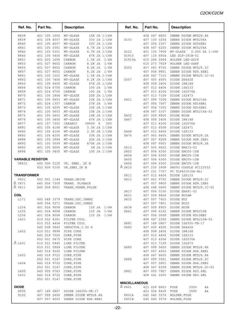
Chassis Electrical Parts List
Ref. No. Part No. Description Ref. No. Part No. Description
Product safety should be considered when a component replacement is made in any area of a receiver. Components indicated by a mark in this parts list and the circuit diagram show components whose value havespecial significance to product safety. It is particularly recommended that only parts specified on the following partslist be used for components replacement pointed out by the mark.
!
Note: Parts order must contain Service Ref. No., Part No., and descriptions. The main PCB unit will be supplied without tuner andflyback transformer. They should be ordered separately.
Read description in the Capacitor and Resistor as follows:
CAPACITORCERAMIC 100P K 50V
Rated Voltage
Tolerance Symbols:Less than 10pFA : Not specified B : ±0.1pF C : ±0.25pFD : ±0.5pF F : ±1PF G : ±2pFR : ±0.25-0pF S : ±0-0.25pF E : +0-1pFMore than 10pFA : Not specified B : ±0.1% C : ±0.25%D : ±0.5% F : ±1% G : ±2%H : ±3% J : ±5% K : ±10%L : ±15% M : ±20% N : ±30%P : +100-0% Q : +30-10% T : +50-10%U : +75-10% V : +20-10% W : +100-10%X : +40-20% Y : +150-10% Z : +80-20%
Rated value: P=pico farad, U=micro farad
Material:CERAMIC........... CeramicMT-PAPER......... Metallized PaperPOLYESTER...... PolyesterMT-POLYEST.....Metallized PolyesterPOLYPRO.......... PolypropyleneMT-POLYPRO....Metallized PolypropyleneCOMPO FILM.....Composite filmMT-COMPO........Metallized CompositeSTYRENE...........StyreneTA-SOLID........... Tantalum SolidAL-SOLID........... Aluminium SolidELECT................ElectrolyticNP-ELECT..........Non-polarised ElectrolyticOS-SOLID.......... Aluminium Solid with Organic Semiconductive ElectrolyticDL-ELECT.......... Double Layered Electrolytic
RESISTORCARBON 4.7K J A 1/4W
Rated Wattage
Performance Symbols:A: General B: Non flammable Z: Low noiseOther: Temperature coefficient
Tolerance Symbols:A: ±0.05% B: ±0.1% C: ±0.25% D: ±0.5%F: ±1% G: ±2% J: ±5% K: ±10%M: ±20% P: +5-15%
Rated value, ohms:K: 1,000, M: 1,000,000
Material:CARBON........... CarbonMT-FILM............ Metal FilmOXIDE-MT......... Oxide Metal FilmSOLID................ CompositionMT-GLAZE......... Metal GlazeWIRE WOUND...Wire WoundCERAMIC RES.. CeramicFUSIBLE RES....Fusible
NOTES:
!
!
!
!
Service Ref. No. CP14SR1-50, CP14SR1(G)-50 CP14SR1-60, CP14SR1(G)-60

Q684 405 011 8401 TR 2SC1740S-Q 405 011 8500 TR 2SC1740S-R 405 011 8609 TR 2SC1740S-S 405 012 2002 TR 2SC1815-GR 405 012 2101 TR 2SC1815-O 405 012 2309 TR 2SC1815-Y 405 020 7501 TR 2SC945A-PA 405 020 7709 TR 2SC945A-QA 405 020 7907 TR 2SC945A-RA
Q685 405 014 4509 TR 2SC2412K T146 R 405 014 4608 TR 2SC2412K T146 S 405 015 8704 TR 2SC2812-L6-TB 405 015 8902 TR 2SC2812-L7-TB 405 173 9803 TR 2SC3928A1R 405 173 9902 TR 2SC3928A1S
Q686 405 134 5905 TR 2SA1037AK-T146-R 405 147 2205 TR 2SA1037AK-S-T146 405 002 0308 TR 2SA1037K T146 R 405 002 0407 TR 2SA1037K T146 S 405 002 6706 TR 2SA1179-M6-TB 405 002 6904 TR 2SA1179-M7-TB 405 173 9605 TR 2SA1235A1E 405 173 9704 TR 2SA1235A1F
Q818 405 014 4509 TR 2SC2412K T146 R 405 014 4608 TR 2SC2412K T146 S 405 015 8704 TR 2SC2812-L6-TB 405 015 8902 TR 2SC2812-L7-TB 405 173 9803 TR 2SC3928A1R 405 173 9902 TR 2SC3928A1S
Q861 405 134 5905 TR 2SA1037AK-T146-R 405 147 2205 TR 2SA1037AK-S-T146 405 002 0308 TR 2SA1037K T146 R 405 002 0407 TR 2SA1037K T146 S 405 002 6706 TR 2SA1179-M6-TB 405 002 6904 TR 2SA1179-M7-TB 405 173 9605 TR 2SA1235A1E 405 173 9704 TR 2SA1235A1F
Q871 405 014 4509 TR 2SC2412K T146 R 405 014 4608 TR 2SC2412K T146 S 405 015 8704 TR 2SC2812-L6-TB 405 015 8902 TR 2SC2812-L7-TB 405 173 9803 TR 2SC3928A1R 405 173 9902 TR 2SC3928A1S
Q881 405 014 4509 TR 2SC2412K T146 R 405 014 4608 TR 2SC2412K T146 S 405 015 8704 TR 2SC2812-L6-TB 405 015 8902 TR 2SC2812-L7-TB 405 173 9803 TR 2SC3928A1R 405 173 9902 TR 2SC3928A1S
Q886 405 014 4509 TR 2SC2412K T146 R 405 014 4608 TR 2SC2412K T146 S 405 015 8704 TR 2SC2812-L6-TB 405 015 8902 TR 2SC2812-L7-TB 405 173 9803 TR 2SC3928A1R 405 173 9902 TR 2SC3928A1S
INTEGRATED CIRCUIT IC001 409 472 4408 IC LA4266 IC201 409 517 5902 IC LA76818A IC202 409 241 5407 IC BA178M05T
409 265 4806 IC L78M05CV 409 172 1509 IC MC78M05CT 409 320 5700 IC UPC78M05AHF
IC501 409 449 4103 IC LA78040 409 507 0900 IC LA78040N
IC651 409 241 5407 IC BA178M05T 409 265 4806 IC L78M05CV
409 172 1509 IC MC78M05CT 409 320 5700 IC UPC78M05AHF
IC801 410 406 3305 IC LC863440V-5Y67-TLM IC802 409 528 8602 IC S524A60X81-DCB0
409 383 6805 IC 24LC08B/P
CAPACITOR C003 404 089 7200 ELECT 100U M 25V
403 044 9501 ELECT 100U M 25V C004 404 084 9209 ELECT 4.7U M 50V
403 051 0607 ELECT 4.7U M 50V C005 404 089 7200 ELECT 100U M 25V
403 044 9501 ELECT 100U M 25V C006 404 087 5109 ELECT 470U M 25V
403 047 5005 ELECT 470U M 25V C007 403 057 3107 POLYESTER 0.1U K 50V
403 181 8207 POLYESTER 0.1U K 50V C008 404 084 8400 ELECT 1000U M 25V
403 045 1504 ELECT 1000U M 25V C012 403 215 2201 CERAMIC 0.01U K 50V C1001 404 084 8905 ELECT 10U M 50V
403 049 4204 ELECT 10U M 50V C1002 404 084 8806 ELECT 1U M 50V
403 049 0008 ELECT 1U M 50V C1003 403 049 4204 ELECT 10U M 50V C1004 403 043 0202 ELECT 220U M 16V C101 404 084 8301 ELECT 470U M 16V
403 044 1703 ELECT 470U M 16V C106 404 084 9308 ELECT 47U M 50V
403 051 3103 ELECT 47U M 50V C107 404 084 9308 ELECT 47U M 50V
403 051 3103 ELECT 47U M 50V C111 403 215 2201 CERAMIC 0.01U K 50V C112 403 215 2201 CERAMIC 0.01U K 50V C113 403 215 2201 CERAMIC 0.01U K 50V C120 403 284 4304 CERAMIC 0.022U K 50V C121 403 215 2201 CERAMIC 0.01U K 50V C122 404 084 7809 ELECT 100U M 16V
403 042 2405 ELECT 100U M 16V C123 401 105 7909 MT-GLAZE 0.000 ZA 1/16W C132 404 084 8707 ELECT 0.47U M 50V
403 048 6308 ELECT 0.47U M 50V C135 404 084 8707 ELECT 0.47U M 50V
403 048 6308 ELECT 0.47U M 50V C138 403 284 4304 CERAMIC 0.022U K 50V C171 403 113 3805 CERAMIC 1000P K 50V C172 403 367 0407 CERAMIC 0.1U K 50V C174 403 157 1904 CERAMIC 10P D 50V C178 404 084 8806 ELECT 1U M 50V
403 049 0008 ELECT 1U M 50V C1902 404 087 5406 ELECT 22U M 50V
403 050 2800 ELECT 22U M 50V C201 404 084 9803 NP-ELECT 1U M 50V
403 086 2300 NP-ELECT 1U M 50V C202 403 058 2604 POLYESTER 0.015U J 50V
403 179 3207 POLYESTER 0.015U J 50V C203 403 215 2201 CERAMIC 0.01U K 50V C204 404 084 8905 ELECT 10U M 50V
403 049 4204 ELECT 10U M 50V C205 404 084 8905 ELECT 10U M 50V
403 049 4204 ELECT 10U M 50V C208 403 367 0407 CERAMIC 0.1U K 50V C209 404 084 8707 ELECT 0.47U M 50V
403 048 6308 ELECT 0.47U M 50V C210 404 084 8301 ELECT 470U M 16V
403 051 4209 ELECT 470U M 50V C211 403 367 0407 CERAMIC 0.1U K 50V
-19-
C2CK/C2CM
Ref. No. Part No. Description Ref. No. Part No. Description

-20-
C2CK/C2CM
C212 403 155 4204 CERAMIC 15P J 50V C221 403 305 3507 CERAMIC 0.1U Z 50V C222 403 305 3507 CERAMIC 0.1U Z 50V C223 403 305 3507 CERAMIC 0.1U Z 50V C224 403 367 0407 CERAMIC 0.1U K 50V C225 404 084 8806 ELECT 1U M 50V
403 049 0008 ELECT 1U M 50V C226 404 084 8806 ELECT 1U M 50V
403 049 0008 ELECT 1U M 50V C230 403 215 2201 CERAMIC 0.01U K 50V C231 403 260 2904 MT-COMPO 0.33U J 50V C232 403 260 2904 MT-COMPO 0.33U J 50V C233 404 084 8905 ELECT 10U M 50V
403 049 4204 ELECT 10U M 50V C234 403 215 2201 CERAMIC 0.01U K 50V C243 403 215 2201 CERAMIC 0.01U K 50V C244 404 084 9308 ELECT 47U M 50V
403 051 3103 ELECT 47U M 50V C245 404 084 9803 NP-ELECT 1U M 50V
403 086 2300 NP-ELECT 1U M 50V C246 404 084 8806 ELECT 1U M 50V
403 049 0008 ELECT 1U M 50V C247 404 084 9001 ELECT 2.2U M 50V
403 049 9803 ELECT 2.2U M 50V C273 403 164 0204 CERAMIC 0.1U Z 25V C283 403 215 2201 CERAMIC 0.01U K 50V C358 404 084 8806 ELECT 1U M 50V
403 049 0008 ELECT 1U M 50V C432 403 075 7101 CERAMIC 1000P K 500V C433 403 076 3102 CERAMIC 3900P K 500V C434 404 087 6007 ELECT 47U M 35V
403 054 0703 ELECT 47U M 35V C435 404 066 5106 MT-POLYPRO 5400P H 1.5K C436 403 275 8403 CERAMIC 390P K 3K C441 403 349 3501 MT-POLYPRO 0.36U J 200V
403 346 7304 MT-POLYPRO 0.36U J 250V C469 404 084 8905 ELECT 10U M 50V
403 049 4204 ELECT 10U M 50V C471 404 056 5307 NP-ELECT 2.2U M 100V
404 084 9902 NP-ELECT 2.2U M 100V C482 404 084 8400 ELECT 1000U M 25V
403 045 1504 ELECT 1000U M 25V C510 404 088 7300 ELECT 22U M 16V
403 042 7707 ELECT 22U M 16V C514 404 084 8905 ELECT 10U M 50V
403 049 4204 ELECT 10U M 50V C515 404 084 8400 ELECT 1000U M 25V
403 045 1504 ELECT 1000U M 25V C517 404 084 9407 ELECT 220U M 35V
403 053 2104 ELECT 220U M 35V C518 403 072 9405 CERAMIC 3300P K 50V C521 404 084 9506 ELECT 470U M 35V
403 054 1502 ELECT 470U M 35V C524 403 064 1202 POLYESTER 0.1U K 100V
403 276 9706 POLYESTER 0.1U K 100V C601 404 093 6107 MT-POLYEST 0.1U M 275V
404 089 1505 MT-POLYEST 0.1U M 275V C602 404 093 6107 MT-POLYEST 0.1U M 275V
404 089 1505 MT-POLYEST 0.1U M 275V C607 404 038 1600 ELECT 100U M 400V
404 067 4009 ELECT 100U M 400V C608 403 247 6505 CERAMIC 680P K 1K
403 271 9800 CERAMIC 680P K 1K C610 403 049 0008 ELECT 1U M 50V C611 403 247 1609 CERAMIC 220P K 1K C612 403 237 8007 MT-COMPO 0.1U J 50V
403 243 6806 MT-COMPO 0.1U J 50V
C613 403 178 9408 POLYESTER 0.012U J 50V 403 249 8903 MT-COMPO 0.012U J 50V
C614 403 056 9704 POLYESTER 0.01U J 50V 403 178 9309 POLYESTER 0.01U J 50V
C627 404 073 5106 CERAMIC 470P K 250V 404 073 3300 CERAMIC 470P M 250V
C629 404 073 3904 CERAMIC 1000P K 250V 404 073 2105 CERAMIC 1000P M 250V 404 088 3104 CERAMIC 1000P M 250V
C631 403 247 5003 CERAMIC 470P K 1K 403 269 1809 CERAMIC 470P K 1K
C633 403 247 5003 CERAMIC 470P K 1K 403 269 1809 CERAMIC 470P K 1K
C634 403 247 5003 CERAMIC 470P K 1K 403 269 1809 CERAMIC 470P K 1K
C641 404 080 0606 ELECT 100U M 160V C643 404 084 9506 ELECT 470U M 35V
403 054 1502 ELECT 470U M 35V C644 404 084 8400 ELECT 1000U M 25V
403 045 1504 ELECT 1000U M 25V C651 403 039 9004 ELECT 1000U M 10V C661 404 084 8806 ELECT 1U M 50V
403 049 0008 ELECT 1U M 50V C662 404 084 7908 ELECT 1000U M 16V
403 042 4805 ELECT 1000U M 16V C685 404 084 8806 ELECT 1U M 50V
403 049 0008 ELECT 1U M 50V C801 403 155 4204 CERAMIC 15P J 50V C802 403 157 2505 CERAMIC 27P J 50V C803 403 215 2201 CERAMIC 0.01U K 50V C805 404 084 7700 ELECT 10U M 16V
403 041 8804 ELECT 10U M 16V C823 403 342 3300 CERAMIC 0.1U K 25V C824 403 367 0407 CERAMIC 0.1U K 50V C825 403 157 3601 CERAMIC 100P J 50V C829 403 342 3300 CERAMIC 0.1U K 25V C835 404 084 8806 ELECT 1U M 50V
403 049 0008 ELECT 1U M 50V C851 403 157 3106 CERAMIC 56P J 50V C852 403 157 3106 CERAMIC 56P J 50V C853 403 157 3106 CERAMIC 56P J 50V C861 404 084 8806 ELECT 1U M 50V
403 049 0008 ELECT 1U M 50V C888 403 155 2200 CERAMIC 3300P K 50V C892 403 342 3300 CERAMIC 0.1U K 25V C893 404 084 9001 ELECT 2.2U M 50V
403 049 9803 ELECT 2.2U M 50V C894 403 281 5007 CERAMIC 0.033U K 25V
RESISTORR003 401 113 5607 MT-GLAZE 750 JA 1/16W R004 401 105 0702 MT-GLAZE 100K JA 1/16W R005 401 025 1308 CARBON 150 JA 1/6W R006 401 024 5604 CARBON 1 JA 1/6W R010 401 105 3307 MT-GLAZE 2.7K JA 1/16W R011 401 105 2904 MT-GLAZE 22K JA 1/16W R1001 401 027 6608 CARBON 75 JA 1/6W R1002 401 024 7004 CARBON 1K JA 1/6W R1003 401 024 7707 CARBON 100K JA 1/6W R1004 401 105 6506 MT-GLAZE 680 JA 1/16W R1005 401 105 0702 MT-GLAZE 100K JA 1/16W R1006 401 027 6608 CARBON 75 JA 1/6W R1007 401 024 7707 CARBON 100K JA 1/6W R103 401 061 8101 OXIDE-MT 39K JA 1W R106 401 024 6700 CARBON 100 JA 1/6W R107 401 024 6700 CARBON 100 JA 1/6W R108 401 105 2102 MT-GLAZE 18K JA 1/16W
Ref. No. Part No. Description Ref. No. Part No. Description
!
!
!

R109 401 105 8203 MT-GLAZE 68K JA 1/16W R111 401 105 0504 MT-GLAZE 1K JA 1/16W R112 401 105 6001 MT-GLAZE 5.6K JA 1/16W R114 401 105 4007 MT-GLAZE 330 JA 1/16W R115 401 027 2105 CARBON 56 JA 1/6W R116 401 105 5806 MT-GLAZE 56 JA 1/16W R130 401 105 7909 MT-GLAZE 0.000 ZA 1/16W R132 401 105 5202 MT-GLAZE 470 JA 1/16W R140 401 105 5905 MT-GLAZE 560 JA 1/16W R141 401 105 5905 MT-GLAZE 560 JA 1/16W R176 401 105 0603 MT-GLAZE 10K JA 1/16W R185 401 068 1600 OXIDE-MT 4.7 JA 2W R1902 401 105 3406 MT-GLAZE 27K JA 1/16W R1903 401 105 1105 MT-GLAZE 12K JA 1/16W R1904 401 105 6001 MT-GLAZE 5.6K JA 1/16W R1905 401 105 4601 MT-GLAZE 3.9K JA 1/16W R1906 401 105 2805 MT-GLAZE 2.2K JA 1/16W R1907 401 024 6700 CARBON 100 JA 1/6W R1911 401 105 2706 MT-GLAZE 220 JA 1/16W R1912 401 105 2706 MT-GLAZE 220 JA 1/16W R1913 401 105 2706 MT-GLAZE 220 JA 1/16W R209 401 113 9506 MT-GLAZE 620K JA 1/16W R210 401 105 3703 MT-GLAZE 3K JA 1/16W R211 401 025 1308 CARBON 150 JA 1/6W R212 401 025 1308 CARBON 150 JA 1/6W R221 401 105 0504 MT-GLAZE 1K JA 1/16W R222 401 105 0504 MT-GLAZE 1K JA 1/16W R223 401 105 0504 MT-GLAZE 1K JA 1/16W R224 401 105 5301 MT-GLAZE 4.7K JA 1/16W R225 401 105 5301 MT-GLAZE 4.7K JA 1/16W R226 401 105 3406 MT-GLAZE 27K JA 1/16W R227 401 105 4205 MT-GLAZE 33K JA 1/16W R228 401 024 7707 CARBON 100K JA 1/6W R229 401 105 6704 MT-GLAZE 680K JA 1/16W R230 401 026 9303 CARBON 47 JA 1/6W R244 401 105 5400 MT-GLAZE 47K JA 1/16W R245 401 105 5400 MT-GLAZE 47K JA 1/16W R263 401 105 0603 MT-GLAZE 10K JA 1/16W R264 401 026 0607 CARBON 270 JA 1/6W R265 401 105 3901 MT-GLAZE 33 JA 1/16W R267 401 026 0607 CARBON 270 JA 1/6W R271 401 105 0405 MT-GLAZE 100 JA 1/16W R272 401 105 0405 MT-GLAZE 100 JA 1/16W R280 401 024 6700 CARBON 100 JA 1/6W R282 401 105 4106 MT-GLAZE 3.3K JA 1/16W R284 401 105 4106 MT-GLAZE 3.3K JA 1/16W R286 401 203 9904 MT-GLAZE 4.7K FA 1/16W R340 401 105 7503 MT-GLAZE 82K JA 1/16W R351 401 027 8602 CARBON 8.2K JA 1/6W R352 401 012 7009 CARBON 10K JA 1/4W R354 401 025 8208 CARBON 22K JA 1/6W R355 401 015 3800 CARBON 18K JA 1/4W R356 401 105 0603 MT-GLAZE 10K JA 1/16W R357 401 026 7002 CARBON 3.9K JA 1/6W R358 401 105 7909 MT-GLAZE 0.000 ZA 1/16W R422 401 023 3700 CARBON 82K JA 1/4W R423 401 023 3700 CARBON 82K JA 1/4W R424 401 024 7004 CARBON 1K JA 1/6W R426 401 024 7400 CARBON 10K JA 1/6W R432 401 024 7004 CARBON 1K JA 1/6W R433 401 007 1104 CARBON 1K JA 1/2W R434 401 008 6702 CARBON 220 JA 1/2W R445 401 068 7800 OXIDE-MT 560 JA 2W R475 401 009 5803 CARBON 330 JA 1/2W R479 401 025 7805 CARBON 2.2K JA 1/6W R481 401 068 1600 OXIDE-MT 4.7 JA 2W R501 401 066 1404 OXIDE-MT 1.8K JA 2W
R510 401 025 8208 CARBON 22K JA 1/6W R511 401 024 7400 CARBON 10K JA 1/6W R514 401 025 1902 CARBON 15K JA 1/6W R515 401 026 1307 CARBON 27K JA 1/6W R516 401 027 2600 CARBON 5.6K JA 1/6W R518 401 009 3106 CARBON 3.3 JA 1/2W R522 401 024 9008 CARBON 120 JA 1/6W R525 401 008 6702 CARBON 220 JA 1/2W R602 402 060 8109 WIRE WOUND 3.9 KA 5W R603 401 010 9203 CARBON 560K JA 1/2W R604 401 066 9103 OXIDE-MT 27 JA 2W R605 401 010 9203 CARBON 560K JA 1/2W R606 401 027 0507 CARBON 470K JA 1/6W R607 401 019 9600 CARBON 47 JA 1/4W R609 401 025 8208 CARBON 22K JA 1/6W R611 401 025 8208 CARBON 22K JA 1/6W R612 402 001 8502 FUSIBLE RES 10 J- 1/2W R613 401 064 3806 OXIDE-MT 1.0 JA 2W R615 401 016 1508 CARBON 22 JA 1/4W R616 401 024 7400 CARBON 10K JA 1/6W R617 402 001 8106 FUSIBLE RES 680 J- 1/4W R618 401 024 7004 CARBON 1K JA 1/6W R619 401 025 8208 CARBON 22K JA 1/6W R620 401 020 0801 CARBON 470 JA 1/4W R628 402 000 8305 SOLID 5.6M KA 1/2W R629 402 000 8305 SOLID 5.6M KA 1/2W R635 401 007 2309 CARBON 100K JA 1/2W R636 401 105 5301 MT-GLAZE 4.7K JA 1/16W R637 401 007 9308 CARBON 150K JA 1/2W R638 401 061 4400 OXIDE-MT 33K JA 1W R639 401 013 6407 CARBON 12K JA 1/4W R642 401 012 7009 CARBON 10K JA 1/4W R643 402 001 8700 FUSIBLE RES 18 J- 1/2W R644 401 142 9508 OXIDE-MT 0.27 JA 1W R645 401 026 3905 CARBON 330 JA 1/6W R646 401 026 1307 CARBON 27K JA 1/6W R661 401 060 7402 OXIDE-MT 270 JA 1W R662 401 066 3002 OXIDE-MT 2.2 JA 2W R663 401 013 6407 CARBON 12K JA 1/4W R681 401 024 7004 CARBON 1K JA 1/6W R682 401 025 8208 CARBON 22K JA 1/6W R683 401 105 6100 MT-GLAZE 560K JA 1/16W R684 401 105 0603 MT-GLAZE 10K JA 1/16W R685 401 105 2904 MT-GLAZE 22K JA 1/16W R688 401 025 8208 CARBON 22K JA 1/6W R689 401 027 3201 CARBON 560K JA 1/6W R801 401 105 3505 MT-GLAZE 270K JA 1/16W R804 401 105 7909 MT-GLAZE 0.000 ZA 1/16W R805 401 105 7909 MT-GLAZE 0.000 ZA 1/16W R811 401 105 3406 MT-GLAZE 27K JA 1/16W R812 401 105 0603 MT-GLAZE 10K JA 1/16W R813 401 105 0603 MT-GLAZE 10K JA 1/16W R814 401 105 0603 MT-GLAZE 10K JA 1/16W R815 401 105 0603 MT-GLAZE 10K JA 1/16W R816 401 105 0603 MT-GLAZE 10K JA 1/16W R817 401 105 3307 MT-GLAZE 2.7K JA 1/16W R818 401 024 7004 CARBON 1K JA 1/6W R819 401 105 0603 MT-GLAZE 10K JA 1/16W R821 401 105 0603 MT-GLAZE 10K JA 1/16W R822 401 105 7909 MT-GLAZE 0.000 ZA 1/16W R830 401 105 0504 MT-GLAZE 1K JA 1/16W R831 401 105 5202 MT-GLAZE 470 JA 1/16W R833 401 105 0603 MT-GLAZE 10K JA 1/16W R834 401 105 0603 MT-GLAZE 10K JA 1/16W R835 401 105 0603 MT-GLAZE 10K JA 1/16W R836 401 105 0603 MT-GLAZE 10K JA 1/16W R837 401 105 1600 MT-GLAZE 15K JA 1/16W
-21-
C2CK/C2CM
Ref. No. Part No. Description Ref. No. Part No. Description
!
!
-22-
C2CK/C2CM
R838 401 105 1600 MT-GLAZE 15K JA 1/16W R839 401 105 4007 MT-GLAZE 330 JA 1/16W R840 401 105 4007 MT-GLAZE 330 JA 1/16W R841 401 105 5301 MT-GLAZE 4.7K JA 1/16W R842 401 105 5301 MT-GLAZE 4.7K JA 1/16W R845 401 105 5400 MT-GLAZE 47K JA 1/16W R851 401 025 1605 CARBON 1.5K JA 1/6W R853 401 027 8602 CARBON 8.2K JA 1/6W R855 401 027 8602 CARBON 8.2K JA 1/6W R857 401 027 8602 CARBON 8.2K JA 1/6W R861 401 105 1501 MT-GLAZE 1.5K JA 1/16W R862 401 105 7404 MT-GLAZE 8.2K JA 1/16W R863 401 105 5400 MT-GLAZE 47K JA 1/16W R866 401 024 6700 CARBON 100 JA 1/6W R869 401 024 6700 CARBON 100 JA 1/6W R870 401 105 2904 MT-GLAZE 22K JA 1/16W R871 401 105 0603 MT-GLAZE 10K JA 1/16W R872 401 026 1307 CARBON 27K JA 1/6W R873 401 105 4205 MT-GLAZE 33K JA 1/16W R874 401 105 0603 MT-GLAZE 10K JA 1/16W R875 401 105 0603 MT-GLAZE 10K JA 1/16W R876 401 105 5400 MT-GLAZE 47K JA 1/16W R877 403 157 7203 CERAMIC 3900P K 50V R881 401 105 4106 MT-GLAZE 3.3K JA 1/16W R882 401 105 4106 MT-GLAZE 3.3K JA 1/16W R883 401 105 4205 MT-GLAZE 33K JA 1/16W R886 401 105 2904 MT-GLAZE 22K JA 1/16W R892 401 105 5509 MT-GLAZE 470K JA 1/16W R893 401 105 8005 MT-GLAZE 1M JA 1/16W R894 401 105 0405 MT-GLAZE 100 JA 1/16W
VARIABLE RESISTORVR631 645 006 5125 VR, SEMI, 2K N
652 000 0100 VR,SEMI,2K N
TRANSFORMER T431 652 001 1144 TRANS,DRIVE T471 645 056 7209 TRANS, FLYBACK T611 645 058 8051 TRANS,POWER,PULSE
COIL L171 645 049 3379 TRANS,OSC,38MHZ
645 054 0271 TRANS,OSC,38MHZ L234 401 024 9008 CARBON 120 JA 1/6W L235 401 024 9008 CARBON 120 JA 1/6W L236 401 024 9008 CARBON 120 JA 1/6W L431 610 032 4381 FILTER COIL
610 032 4404 FILTER COIL 645 008 5642 INDUCTOR,3.3U K
L432 610 031 9998 PIPE CORE 645 018 7025 CORE,PIPE 652 001 0475 PIPE CORE
L601 610 031 5945 LINE FILTER 610 031 5969 LINE FILTER 645 018 9265 LINE FILTER
L603 645 018 9722 CORE,PIPE 652 001 0147 CORE,PIPE
L604 645 018 9722 CORE,PIPE 652 001 0147 CORE,PIPE
L605 645 005 0763 CORE,PIPE L631 645 018 9722 CORE,PIPE
652 001 0147 CORE,PIPE
DIODE D005 407 149 0807 DIODE 1SS355-TE-17 D102 407 099 5600 ZENER DIODE MTZJ6.8A
407 057 4003 ZENER DIODE RD6.8EB1
408 047 8605 ZENER DIODE MTZJ6.8A D103 407 100 0204 ZENER DIODE MTZJ36A
407 056 2307 ZENER DIODE RD36EB1 408 047 6205 ZENER DIODE MTZJ36A
D122 401 105 7909 MT-GLAZE 0.000 ZA 1/16W D1910 407 116 6504 LED SLP-181B-51 D1910A 610 264 5064 HOLDER LED-S2CP
610 273 7929 HOLDER LED-S4KF D352 407 063 8705 ZENER DIODE MTZJ5.1C
407 056 9801 ZENER DIODE RD5.6EB1 408 047 7103 ZENER DIODE MTZJ5.1C-52
D357 407 005 4505 DIODE DS442X 408 008 2406 DIODE 1N4148 407 012 4406 DIODE 1SS133 407 013 4306 DIODE 1S2076A 407 013 7109 DIODE 1S2473
D421 407 099 7208 ZENER DIODE MTZJ16A 407 054 7007 ZENER DIODE RD16EB1 407 054 7205 ZENER DIODE RD16EB3 408 047 5307 ZENER DIODE MTZJ16A-52
D432 407 009 8905 DIODE RU3M D467 408 008 2406 DIODE 1N4148
407 013 4306 DIODE 1S2076A 407 013 6508 DIODE 1S2471
D468 407 012 4406 DIODE 1SS133 D476 407 063 9405 ZENER DIODE MTZJ8.2A
407 057 8209 ZENER DIODE RD8.2EB1 408 047 9503 ZENER DIODE MTZJ8.2A
D512 407 005 8602 DIODE ERA15-02 D603 407 006 6300 DIODE ERC05-10B D604 407 006 6300 DIODE ERC05-10B D605 407 006 6300 DIODE ERC05-10B D606 407 006 6300 DIODE ERC05-10BD610 407 230 3908 PHOTO COUPLE PC123Y52
407 231 7707 PC TLP421F(D4-BL) D611 407 012 4406 DIODE 1SS133 D613 407 063 9702 ZENER DIODE MTZJ9.1C
407 057 9800 ZENER DIODE RD9.1EB3 408 048 0400 ZENER DIODE MTZJ9.1C-52
D617 407 006 0100 DIODE ERA91-02 D631 407 009 8806 DIODE RU3AM D633 407 007 7603 DIODE EU2
407 007 7801 DIODE EU2Z D634 407 009 8905 DIODE RU3M D661 407 099 6102 ZENER DIODE MTZJ10B
407 054 0008 ZENER DIODE RD10EB2 408 047 2306 ZENER DIODE MTZJ10B-52
D681 407 149 0807 DIODE 1SS355-TE-17 D683 407 005 4505 DIODE DS442X
408 008 2406 DIODE 1N4148 407 012 4406 DIODE 1SS133 407 013 4306 DIODE 1S2076A 407 013 7109 DIODE 1S2473
D685 407 099 5600 ZENER DIODE MTZJ6.8A 407 057 4003 ZENER DIODE RD6.8EB1 408 047 8605 ZENER DIODE MTZJ6.8A
D686 407 099 5501 ZENER DIODE MTZJ6.2C 407 057 2801 ZENER DIODE RD6.2EB3 408 047 8308 ZENER DIODE MTZJ6.2C-52
D861 407 055 7907 ZENER DIODE RD3.6EL 408 041 2005 ZENER DIODE RD3.6EL
MISCELLANEOUSF601 423 028 8603 FUSE 250V 4A
423 024 8409 FUSE 250V 4A F601A 645 040 3576 HOLDER,FUSE F601B 645 040 3576 HOLDER,FUSE
Ref. No. Part No. Description Ref. No. Part No. Description
!
!
!
!
!

A101 645 057 2753 TUNER,U/V 645 061 4132 TUNER,U/V
A1901A 645 047 6228 UNIT,REMOCON RECEIVER K1001 645 061 4248 JACK,RCA-2
652 001 2226 JACK,RCA-2 K1002 645 061 4248 JACK,RCA-2
652 001 2226 JACK,RCA-2 K1003 645 040 1275 JACK,RCA-2
652 001 2202 JACK,RCA-2PS601 408 046 4400 THERMISTOR PTDAA1BF9R0Q20 SW1901 645 003 4701 SWITCH,PUSH 1P-1TX1
645 019 4887 SWITCH,PUSH 1P-1TX1 645 027 7382 SWITCH,PUSH 1P-1TX1
SW1902 645 003 4701 SWITCH,PUSH 1P-1TX1 645 019 4887 SWITCH,PUSH 1P-1TX1 645 027 7382 SWITCH,PUSH 1P-1TX1
SW1903 645 003 4701 SWITCH,PUSH 1P-1TX1 645 019 4887 SWITCH,PUSH 1P-1TX1 645 027 7382 SWITCH,PUSH 1P-1TX1
SW1904 645 003 4701 SWITCH,PUSH 1P-1TX1 645 019 4887 SWITCH,PUSH 1P-1TX1 645 027 7382 SWITCH,PUSH 1P-1TX1
SW1905 645 003 4701 SWITCH,PUSH 1P-1TX1 645 019 4887 SWITCH,PUSH 1P-1TX1 645 027 7382 SWITCH,PUSH 1P-1TX1
SW601 645 059 0061 SWITCH, POWER 1P-1TX1 X161 421 009 4606 SAW F TSF5419P X211 645 024 8818 OSC,CRYSTAL 4.433619MHZ
652 001 0154 OSC,CRYSTAL 4.433619MHZ X801 645 004 1938 OSC,CRYSTAL 32.768KHZ
645 004 1945 OSC,CRYSTAL 32.768KHZ
610 307 2951 ASSY,PWB,CRT C4EY1AA0B10S1140B
TRANSISTORQ701 406 000 5104 TR 2SC2229-O(SAN-2)
406 000 5203 TR 2SC2229-Y(SAN-2) 405 040 5600 TR 2SC2228-D 405 029 6901 TR 2SC2228-E
Q703 406 000 5104 TR 2SC2229-O(SAN-2) 406 000 5203 TR 2SC2229-Y(SAN-2) 405 040 5600 TR 2SC2228-D 405 029 6901 TR 2SC2228-E
Q705 406 000 5104 TR 2SC2229-O(SAN-2) 406 000 5203 TR 2SC2229-Y(SAN-2) 405 040 5600 TR 2SC2228-D 405 029 6901 TR 2SC2228-E
Q721 405 001 7407 TR 2SA1015-O(SAN) 405 001 7605 TR 2SA1015-Y(SAN)
Q751 405 002 0308 TR 2SA1037K T146 R 405 002 0407 TR 2SA1037K T146 S 405 002 6706 TR 2SA1179-M6-TB 405 002 6904 TR 2SA1179-M7-TB 405 173 9605 TR 2SA1235A1E 405 173 9704 TR 2SA1235A1F
CAPACITOR C708 404 084 6505 CERAMIC 1000P K 2K
403 077 2708 CERAMIC 1000P P 2K 403 077 2807 CERAMIC 1000P Z 2K 403 312 8304 CERAMIC 1000P Z 2K
C710 403 368 8907 ELECT 4.7U M 250V C751 404 084 7809 ELECT 100U M 16V
403 042 2405 ELECT 100U M 16V
RESISTOR R701 401 105 7206 MT-GLAZE 82 JA 1/16W R702 401 026 0607 CARBON 270 JA 1/6W R704 401 105 7206 MT-GLAZE 82 JA 1/16W R705 401 026 0607 CARBON 270 JA 1/6W R707 401 105 7206 MT-GLAZE 82 JA 1/16W R708 401 026 0607 CARBON 270 JA 1/6W R711 401 065 4604 OXIDE-MT 12K JA 2W R712 401 065 4604 OXIDE-MT 12K JA 2W R713 401 065 4604 OXIDE-MT 12K JA 2W R715 401 009 1508 CARBON 2.7K JA 1/2W R718 401 009 1508 CARBON 2.7K JA 1/2W R719 401 009 1508 CARBON 2.7K JA 1/2W R723 401 105 1006 MT-GLAZE 1.2K JA 1/16W R724 401 026 9600 CARBON 470 JA 1/6W R743 401 024 9701 CARBON 12K JA 1/6W R751 401 105 1501 MT-GLAZE 1.5K JA 1/16W R752 401 105 0603 MT-GLAZE 10K JA 1/16W R753 401 105 0603 MT-GLAZE 10K JA 1/16W
COILL702 645 007 9337 INDUCTOR,270U K
DIODED741 407 149 0807 DIODE 1SS355-TE-17 D742 407 149 0807 DIODE 1SS355-TE-17 D751 407 149 0807 DIODE 1SS355-TE-17 D752 407 149 0807 DIODE 1SS355-TE-17 D753 407 149 0807 DIODE 1SS355-TE-17 D754 407 149 0807 DIODE 1SS355-TE-17
MISCELLANEOUSK701M 645 025 6097 SOCKET,CRT 8P
-23-
C2CK/C2CM
Ref. No. Part No. Description Ref. No. Part No. Description
!
!
!

SANYO Electric Co., Ltd.A14800/April/’03/30 BB
Printed in Japan