Embed Size (px)
Citation preview

TRC: Oct 25-27, 2004
SER Logic Fail SER Logic Fail DeratingDerating: : Estimating Product FIT RatesEstimating Product FIT Rates
Hang Nguyen and Yoad YagilPrincipal EngineerIntel CorporationChandler, AZ
10/27/2004 • Topical Research Conference on Reliability • Slide 2®®
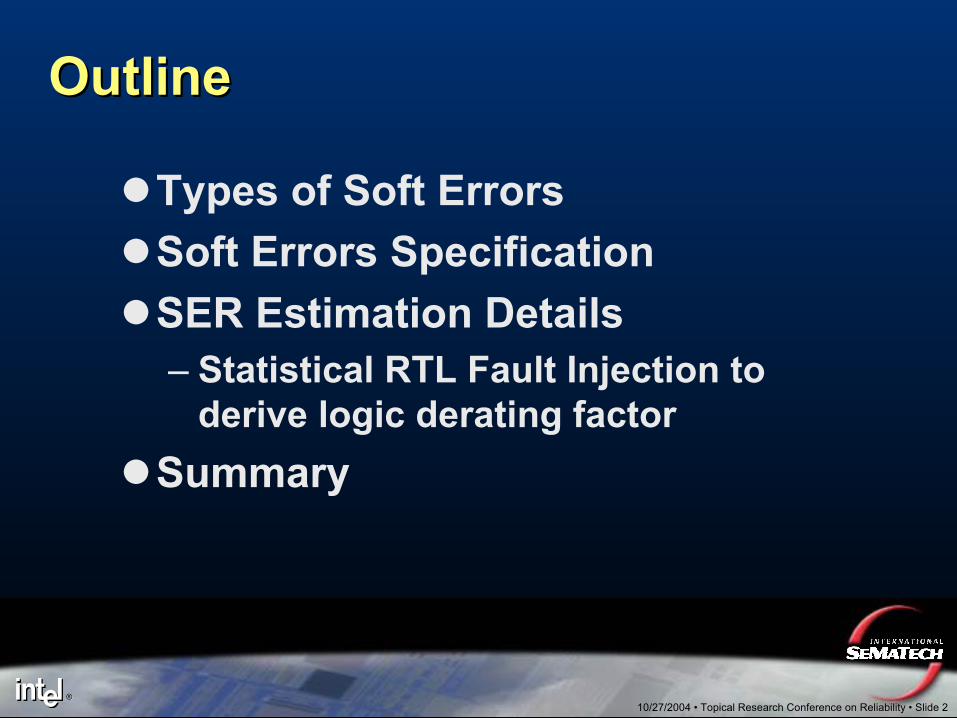
OutlineOutline
Types of Soft Errors Soft Errors SpecificationSER Estimation Details – Statistical RTL Fault Injection to
derive logic derating factorSummary
10/27/2004 • Topical Research Conference on Reliability • Slide 3®®
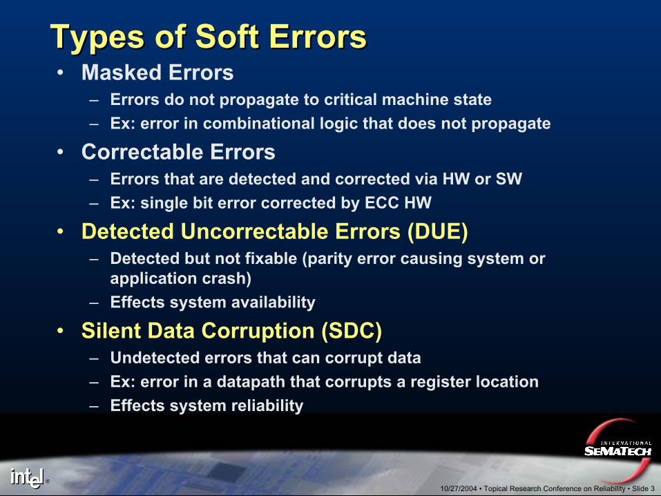
Types of Soft ErrorsTypes of Soft Errors• Masked Errors
– Errors do not propagate to critical machine state– Ex: error in combinational logic that does not propagate
• Correctable Errors– Errors that are detected and corrected via HW or SW– Ex: single bit error corrected by ECC HW
• Detected Uncorrectable Errors (DUE)– Detected but not fixable (parity error causing system or
application crash)– Effects system availability
• Silent Data Corruption (SDC)– Undetected errors that can corrupt data– Ex: error in a datapath that corrupts a register location– Effects system reliability

10/27/2004 • Topical Research Conference on Reliability • Slide 4®®
Sample Soft Errors SpecSample Soft Errors Spec
10 years
25 years1000 years
IBM*
Detected Errors causing application termination (DUE)
Detected Errors causing system termination (DUE)
Silent Data Corruption (SDC)
* D.C.Bossen, IBM Server Group, 2002 Reliability Physics Tutorial, IRPS
• SDC spec is more stringent since error is fatal• DUE spec is more relaxed since error can be
detected and sometimes contained• Per component budget derived from above specs
10/27/2004 • Topical Research Conference on Reliability • Slide 5®®
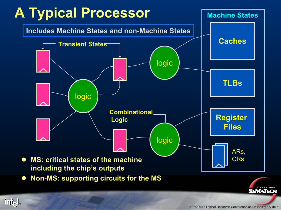
A Typical Processor
Caches
TLBs
Register Files
ARs,CRs
Machine States
logic
logic
logic
Transient States
CombinationalLogic
Includes Machine States and non-Machine States
MS: critical states of the machine including the chip’s outputsNon-MS: supporting circuits for the MS
10/27/2004 • Topical Research Conference on Reliability • Slide 6®®
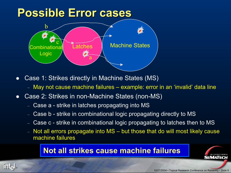
Possible Error casesPossible Error cases
Case 1: Strikes directly in Machine States (MS)– May not cause machine failures – example: error in an ‘invalid’ data line
Case 2: Strikes in non-Machine States (non-MS)– Case a - strike in latches propagating into MS – Case b - strike in combinational logic propagating directly to MS– Case c - strike in combinational logic propagating to latches then to MS– Not all errors propagate into MS – but those that do will most likely cause
machine failures
CombinationalLogic
Latches Machine States
a
c
b
Not all strikes cause machine failures
10/27/2004 • Topical Research Conference on Reliability • Slide 7®®
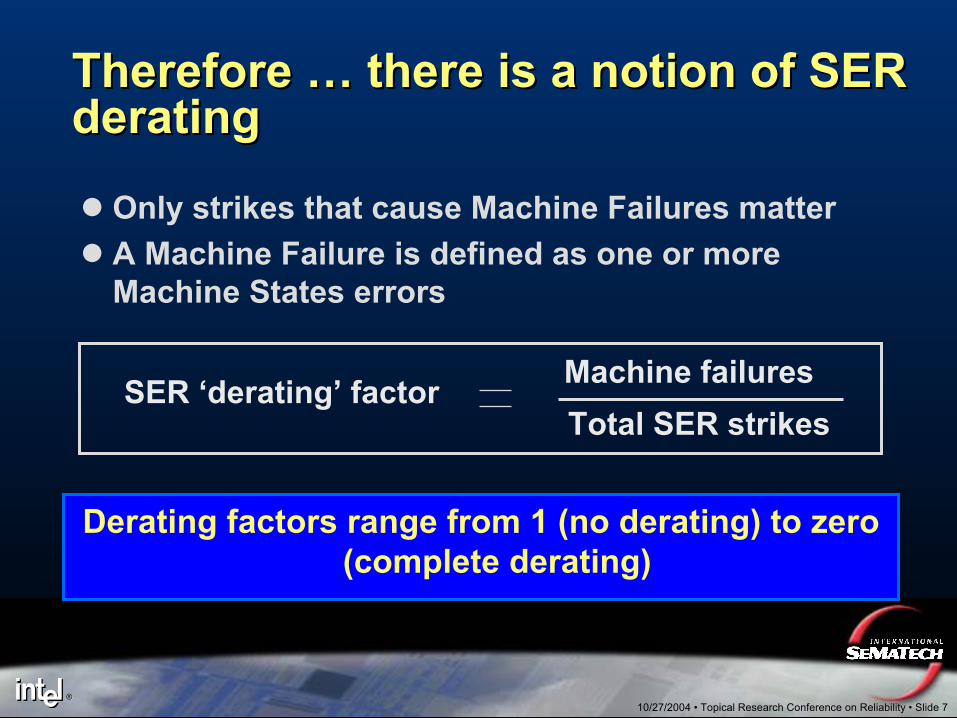
Therefore … there is a notion of SER Therefore … there is a notion of SER deratingderating
SER ‘derating’ factor Machine failuresTotal SER strikes
Only strikes that cause Machine Failures matterA Machine Failure is defined as one or more Machine States errors
Derating factors range from 1 (no derating) to zero (complete derating)

10/27/2004 • Topical Research Conference on Reliability • Slide 8®®
Chip FIT EstimationChip FIT Estimation
Chip FIT rate is the sum of all element FITs on dieNominal FIT – derived from circuit or SER simulations– Failure rate of a circuit element– A function of the circuit topology, device strengths, and
operating conditions (VDD, Temp, Altitude)Derating Factor (DF) includes timing and logic components– Timing Derating (TD) – dependent on the duration the circuit is
sensitive to a strike– Logic Derating (LD) – dependent on how the circuit logically
reacts to a strike. A function of:• The System Application (how the circuit is utilized) AND• The Micro-architecture (how the circuit responds to an error)
∑==
Elements
nDeratingFITChipFIT
1* nominal
10/27/2004 • Topical Research Conference on Reliability • Slide 9®®
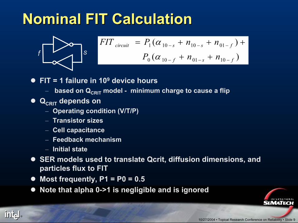
Nominal FIT CalculationNominal FIT Calculation
)(
)(
1001100
0110101
fsf
fsscircuit
nnP
nnPFIT
−−−
−−−
++
+++=
α
α
FIT = 1 failure in 109 device hours – based on QCRIT model - minimum charge to cause a flip
QCRIT depends on – Operating condition (V/T/P) – Transistor sizes– Cell capacitance– Feedback mechanism– Initial state
SER models used to translate Qcrit, diffusion dimensions, and particles flux to FITMost frequently, P1 = P0 = 0.5Note that alpha 0->1 is negligible and is ignored
sf

10/27/2004 • Topical Research Conference on Reliability • Slide 10®®
Machine States FIT EstimateMachine States FIT Estimate∑=
−+
=
)(
1** nominal
ArraysnonArrays
nLDTDFITMSFIT
TD ~1 for ALL MS– MS tend to be of a “storage” nature thus
sensitive most of the timeLD ~1 for non-Array states
– Control and Application registers – These states control the machine
operations and likely to cause machine failure if flipped
LDs for Arrays– Caches, TLBs, Reg Files – Depends on how each array reacts to a
strike - not all strikes are fatal– Can be derived from performance data
ex: % of valid states in arrays
DTLB
Static DominoL2 cache
Clock Latches L1 cache
L3 cache
Floating PointReg File
ITLB
Integer RF
10/27/2004 • Topical Research Conference on Reliability • Slide 11®®
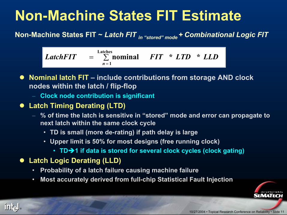
Non-Machine States FIT ~ Latch FIT in “stored” mode + Combinational Logic FIT
Non-Machine States FIT Estimate
∑==
Latches
1** nominal
nLLDLTDFITLatchFIT
Nominal latch FIT – include contributions from storage AND clock nodes within the latch / flip-flop
– Clock node contribution is significantLatch Timing Derating (LTD)
– % of time the latch is sensitive in “stored” mode and error can propagate to next latch within the same clock cycle• TD is small (more de-rating) if path delay is large• Upper limit is 50% for most designs (free running clock)
• TD 1 if data is stored for several clock cycles (clock gating)Latch Logic Derating (LLD)• Probability of a latch failure causing machine failure• Most accurately derived from full-chip Statistical Fault Injection
10/27/2004 • Topical Research Conference on Reliability • Slide 12®®
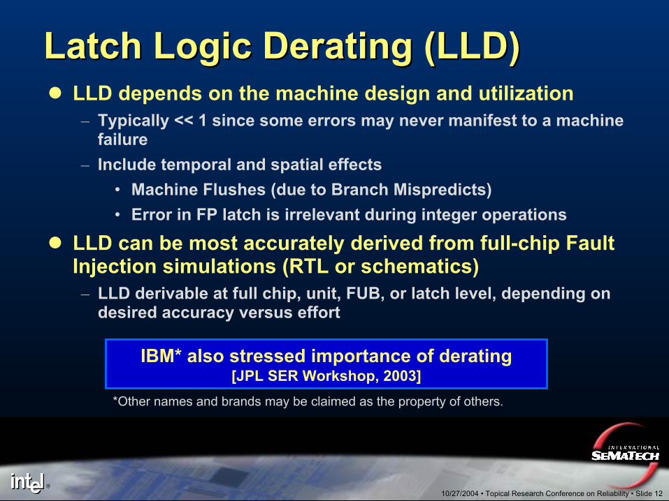
Latch Logic Derating (LLD)Latch Logic Derating (LLD)LLD depends on the machine design and utilization– Typically << 1 since some errors may never manifest to a machine
failure– Include temporal and spatial effects
• Machine Flushes (due to Branch Mispredicts)• Error in FP latch is irrelevant during integer operations
LLD can be most accurately derived from full-chip Fault Injection simulations (RTL or schematics)– LLD derivable at full chip, unit, FUB, or latch level, depending on
desired accuracy versus effort
IBM* also stressed importance of derating[JPL SER Workshop, 2003]
*Other names and brands may be claimed as the property of others.

10/27/2004 • Topical Research Conference on Reliability • Slide 13®®
Statistical RTL Fault Injection to Statistical RTL Fault Injection to derive LLD using 2derive LLD using 2--D samplingD sampling
Using statistics -Latch sample size = 300Time sample size = 1000Each latch maps to 100 time samples giving 30K RTL simulations
0 1B CLK
1000 time samples1 2 1000
300 latch samples
30K RTL simulations to derive chip LLD
Each latch maps to 100 time samples
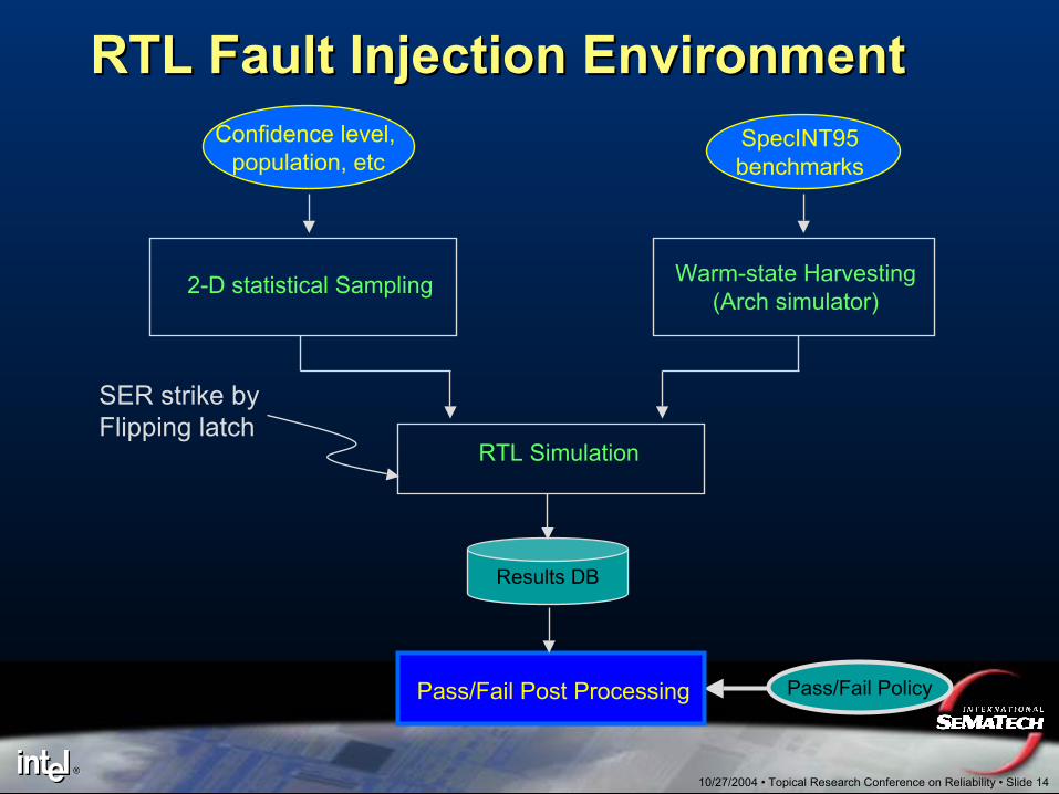
10/27/2004 • Topical Research Conference on Reliability • Slide 14®®
Confidence level, population, etc
2-D statistical Sampling
Pass/Fail Policy
Results DB
SpecINT95 benchmarks
RTL Fault Injection EnvironmentRTL Fault Injection Environment
Warm-state Harvesting(Arch simulator)
RTL Simulation
Pass/Fail Post Processing
SER strike byFlipping latch
10/27/2004 • Topical Research Conference on Reliability • Slide 15®®
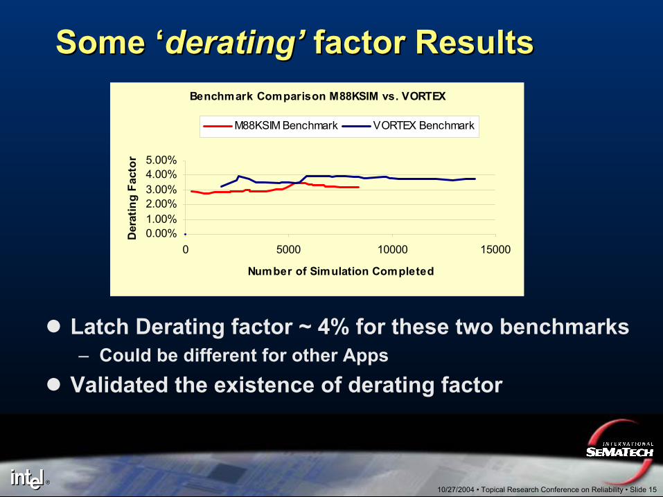
Some ‘Some ‘deratingderating’’ factor Resultsfactor Results
Latch Derating factor ~ 4% for these two benchmarks– Could be different for other Apps
Validated the existence of derating factor
Benchmark Comparison M88KSIM vs. VORTEX
0.00%1.00%2.00%3.00%4.00%5.00%
0 5000 10000 15000
Number of Simulation Completed
Der
atin
g Fa
ctor
M88KSIM Benchmark VORTEX Benchmark
10/27/2004 • Topical Research Conference on Reliability • Slide 16®®
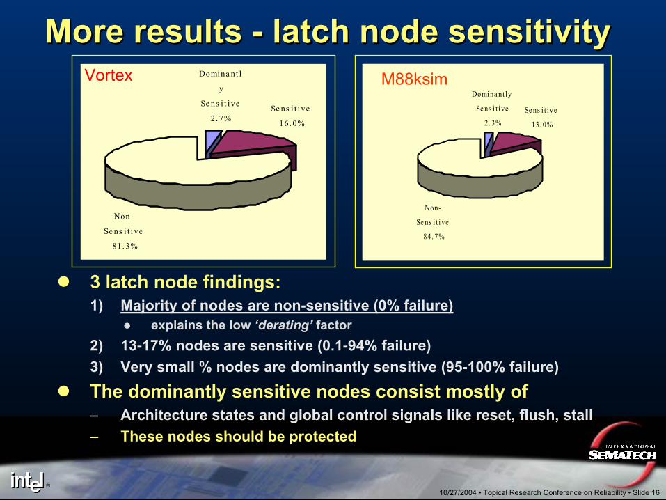
Domina nt ly
Se ns i t i ve
2. 3%Se ns i t i ve
13. 0%
Non-
Se ns i t i ve
84. 7%
More results More results -- latch node sensitivitylatch node sensitivityM88ksim
3 latch node findings: 1) Majority of nodes are non-sensitive (0% failure)
explains the low ‘derating’ factor2) 13-17% nodes are sensitive (0.1-94% failure)3) Very small % nodes are dominantly sensitive (95-100% failure)
The dominantly sensitive nodes consist mostly of – Architecture states and global control signals like reset, flush, stall– These nodes should be protected
Se ns i t i ve
16. 0%
Non-
Se ns i t i ve
81. 3%
Domina nt l
y
Se ns i t i ve
2. 7%
Vortex
10/27/2004 • Topical Research Conference on Reliability • Slide 17®®
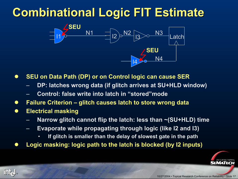
SEU on Data Path (DP) or on Control logic can cause SER– DP: latches wrong data (if glitch arrives at SU+HLD window)– Control: false write into latch in “stored”mode Failure Criterion – glitch causes latch to store wrong dataElectrical masking– Narrow glitch cannot flip the latch: less than ~(SU+HLD) time– Evaporate while propagating through logic (like I2 and I3)
• If glitch is smaller than the delay of slowest gate in the pathLogic masking: logic path to the latch is blocked (by I2 inputs)
Combinational Logic FIT EstimateCombinational Logic FIT Estimate
LatchN1 N2 N3I3I2I1
SEU
N4I4
SEU
10/27/2004 • Topical Research Conference on Reliability • Slide 18®®
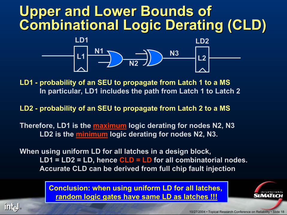
Upper and Lower Bounds of Upper and Lower Bounds of Combinational Logic Combinational Logic DeratingDerating (CLD)(CLD)
LD1 - probability of an SEU to propagate from Latch 1 to a MSIn particular, LD1 includes the path from Latch 1 to Latch 2
LD2 - probability of an SEU to propagate from Latch 2 to a MS
Therefore, LD1 is the maximum logic derating for nodes N2, N3LD2 is the minimum logic derating for nodes N2, N3.
When using uniform LD for all latches in a design block, LD1 = LD2 = LD, hence CLD = LD for all combinatorial nodes.Accurate CLD can be derived from full chip fault injection
Conclusion: when using uniform LD for all latches, random logic gates have same LD as latches !!!
N3N2
N1LD1 LD2
L2L1
10/27/2004 • Topical Research Conference on Reliability • Slide 19®®
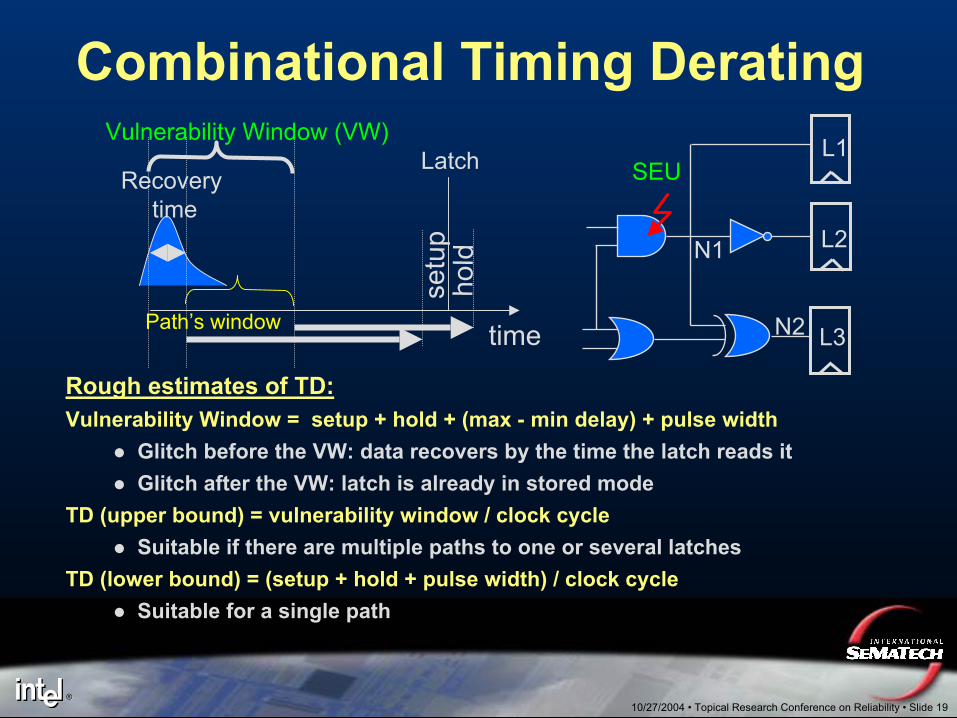
Combinational Timing Derating
Rough estimates of TD:Vulnerability Window = setup + hold + (max - min delay) + pulse width
Glitch before the VW: data recovers by the time the latch reads itGlitch after the VW: latch is already in stored mode
TD (upper bound) = vulnerability window / clock cycleSuitable if there are multiple paths to one or several latches
TD (lower bound) = (setup + hold + pulse width) / clock cycleSuitable for a single path
Latch
setu
pho
ld
Path’s window time
Recoverytime
Vulnerability Window (VW)
N1
N2
L1
L3
L2
SEU

10/27/2004 • Topical Research Conference on Reliability • Slide 20®®
Chip FIT Rate SummaryChip FIT Rate SummaryThree factors make up a device FIT rate: Nominal FIT, TD, LDMS (including caches and register files) occupy most of the area hence dominate the FIT rate and often protected by ECC or parityNon-MS (latches and combinational logic) can become the main SER contributorsCombinational logic FIT can approach latch FIT contributions– Typically, a latch derated FIT can be an order of magnitude larger
than derated FIT of combinational gateNominal Latch FIT is typically larger than that of combinational gateLatch LD ~ combinational LD for most casesLatch TD is larger than combinational TD
– # combinational logic gates can be an order of magnitude higher than # latches
Derating is one of the most effective ways to avoid FIT rate overestimation
![Open Archive TOULOUSE Archive Ouverte (OATAO) · The “Space Product Assurance - Derating - EEE components” ECSS-Q- ST-30-11C [14] specifies electrical derating requirements applicable](https://img.dokumen.tips/doc/110x75/5b9509e309d3f2205c8c0df8/open-archive-toulouse-archive-ouverte-oatao-the-space-product-assurance.jpg)