Embed Size (px)
Citation preview

Special Seminar III
This seminar is dedicated to students taking senior design project or attempting to take it very soon
The focus is on practical aspects of engineering necessary to complete senior design project successfully and professionally
SMT in Practice
Dr. Peter W. PachowiczDepartment of Electrical and Computer Engineering
Volgenau School of Engineering

Goals
To use modern technology available only as SMT components
To understand SMT
To learn SMT soldering and rework techniques
To handle SMT devices with ease
To use senior design lab resources properly and efficiently

Topics
ECE SMT fabrication capabilities
SMT components
SMT tips
SMT soldering techniques
SMT soldering tips
SMT soldering tools
Rework for SMT
Note: Please listen carefully and keep notes. There will be a lot of information provided that is not on these slides.

Additional Resources
Books:
“Mastering Surface Mount Technology,” by V. Himpe
“Surface Mount Technology for PC Boards,” by G. Blackwell & J. Hollmon
On-Line articles:
Intro to SMThttp://www.ece.msstate.edu/~reese/senior_design/pcb/Intro_to_SMT.pdf
Search youtube.com for soldering tips

ECE SMT Fabrication Capabilities
PCB fabrication
Solder paste disposer
IR soldering and rework
Hot air rework, hot tweezers
Quality inspection
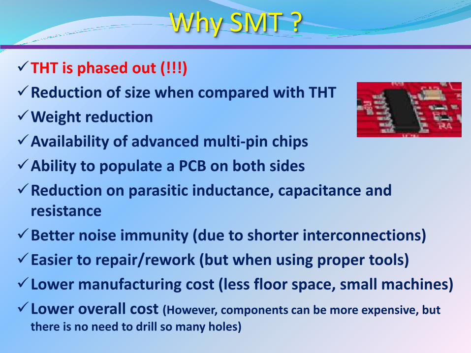
Why SMT ?
THT is phased out (!!!)
Reduction of size when compared with THT
Weight reduction
Availability of advanced multi-pin chips
Ability to populate a PCB on both sides
Reduction on parasitic inductance, capacitance and resistance
Better noise immunity (due to shorter interconnections)
Easier to repair/rework (but when using proper tools)
Lower manufacturing cost (less floor space, small machines)
Lower overall cost (However, components can be more expensive, but
there is no need to drill so many holes)
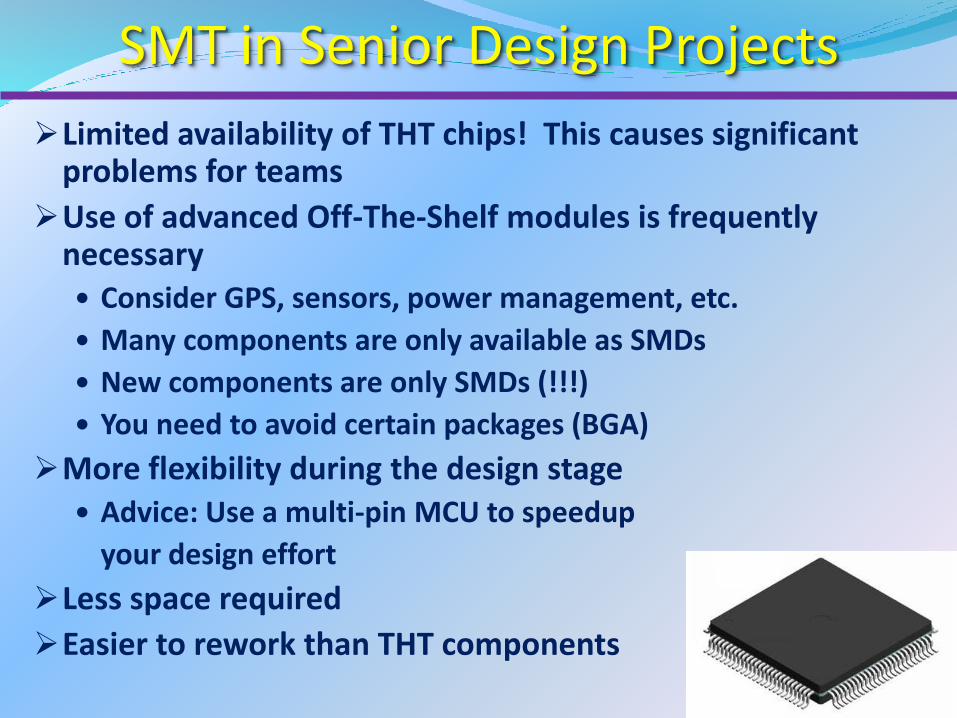
SMT in Senior Design Projects
Limited availability of THT chips! This causes significant problems for teams
Use of advanced Off-The-Shelf modules is frequently necessary Consider GPS, sensors, power management, etc.
Many components are only available as SMDs
New components are only SMDs (!!!)
You need to avoid certain packages (BGA)
More flexibility during the design stage Advice: Use a multi-pin MCU to speedup
your design effort
Less space required
Easier to rework than THT components

SMT Dimensioning
Imperial units are still in use for PCB design
US is the only country left in the world using Imperial units
Think about implications and confusions
Metric units are used most of the time in SMT
Migration to metric is accelerated due to miniaturization
Virtually all new SMDs are metric-dimensioned (!!!)
Plan accordingly when using PCB design software1 mil = 0.0254 mm
Divide your PCB design process into stages and work w/ single dimension units (do not mix them up); e.g.,
1. Sketch board contour inch (or metric) units
2. Assign THT footprints inch units
3. Assign SMD footprints metric (or inch) units
4. Make connections metric (or inch) units

SMT Component Dimensions
Units have implications on device dimension type and indirectly on pad/footprint size
Standardization; e.g.,
Inch notation 1206 implies 0.12”x0.06” (3.048x2.032 mm)
Metric notation 3216 implies 3.2x1.6 mm (0.126”x0.063”)
However, inch 1812 is very similar in size to metric 4532
Plan to work with chips at least 3mm long
Good luck if you decide to work with ultra-small chips
Plan to work with multi-pin chips of pitch >0.5mm
Manual work with pitch 0.5mm or lower is very difficult
If so, allocate a lot of time, be very patient, and learn soldering on a separate breakout board first (!)
Plan to work with larger pads – for easier soldering

SMD Resistor Technology
Standard packages:
0805 (in); 2012 (mm): 0.125W, 150V
1206 (in); 3216 (mm): 0.25W, 200V
1210 (in); 3225 (mm): 0.50W, 200V
1812 (in); 4532 (mm): 0.75W, 200V
Bigger chip higher the cost
Larger chip ratings are really high but the size will make you comfortable to place and solder them
Resistor technology:
Thin film – are of better quality, better tolerances, lower induced noise (E24 and E48 series)
Thick film – low cost, better for very high resistance values >5 MΩ (E12 series)

SMD Resistor Values
No longer color coded
Worse, certain manufactures avoid stamping values
Use a 3 or 4 digit stamped code – it’s a bit of a madhouse
Coding:101 10 followed by 1 zero = 100 Ω
100 10 and 0 zeros = 10 Ω
103 = 10 kΩ
2212 = 22.1 kΩ
10R Most common notation = 10 Ω
8R2 = 8.2 Ω
R100 or R10 = 0.1 Ω
General denomination code
3 digit indicates a 5% part
4 digit indicates a 1% part or better

SMD Capacitor Technology (1)
Standard packages – the same as for SMT resistors
Capacitors have a third dimension
(their thickness) depending on the cap value
Capacitor values are not stamped – don’t mix chips
Ceramic capacitors (general use) come in different grade
NPO, X5R, X7R, Y5V, etc. depending on dielectric material
Highly depend on an application and have tolerances >=10%
Film capacitors
Better quality with tolerances within 5%
Mostly for signal coupling applications in analog electronics

SMD Capacitor Technology (2)
Tantalum Capacitors
Needed, for example, to cut noise in a MCU package
May have different footprints
They have internal fuse and self extinguishing case material
Because, they can malfunction, explode, and/or set fire
They are polarized. It’s important not to reverse voltage on them.
Reverse voltage of 1.5V is enough to cause a catastrophic failure
Electrolytic capacitors
Generally more expensive than ones in THT when ordered in small quantities. Still price is low if you need few of them.
Check footprint spec for one you need (typically: CAN-SMD)

SMD Diodes and Transistors
Diode packages:
SOD-xxx Small Outline Diode
DO-xxx Outline diode
Can be two-, three- or more pin packages (SOT-xxx)
Transistor packages:
SOT-xxx Small Outline Transistor
DPAK and D2PAK
Have minimum three pins (can have more, even to eight pins)
Avoid sizes below 3mm (or <2.5mm)
Attention: diode size can be below 1mm

SMT Integrated Circuits
Contains by far the largest variety of packages
Footprints vary
Dual row style packages
Four sided packages
Complex BGA and QFN style packages
Some of these packages cannot be handled without specialized equipment !
However, there are tricks to solder them properly (ask before working on your own)
I will highlight selected packages which
1. You can solder relatively easily
2. You will need to be very patient
3. You should try to avoid, if possible
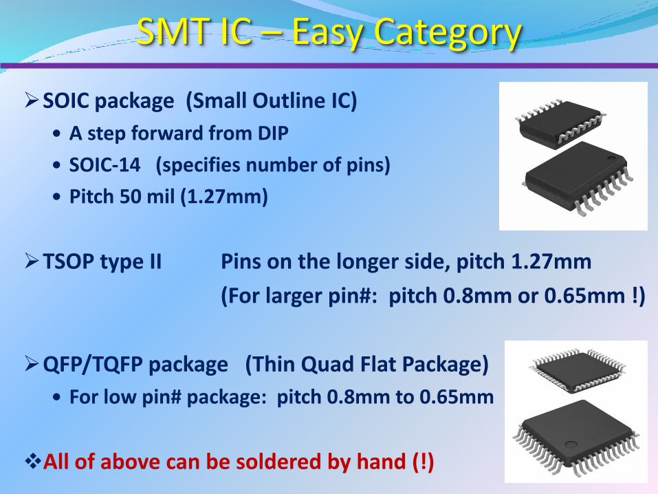
SMT IC – Easy Category
SOIC package (Small Outline IC)
A step forward from DIP
SOIC-14 (specifies number of pins)
Pitch 50 mil (1.27mm)
TSOP type II Pins on the longer side, pitch 1.27mm
(For larger pin#: pitch 0.8mm or 0.65mm !)
QFP/TQFP package (Thin Quad Flat Package)
For low pin# package: pitch 0.8mm to 0.65mm
All of above can be soldered by hand (!)
SMT IC – BeVeryPatient Category
SSOP with pitch 0.65 mm
QFP/TQFP package with larger number of pins (>=64 pins)
Pitch 0.5 mm (you need to be extremely patient)
This is an unavoidable package for many high-pin# MCUs
Practice soldering these chips before the final job
Practice using small breakout boards (cost $5-$7) rather than working directly with your PCB
They can be soldered by hand and traditional iron when: You have experience, work very slowly, and use right tools
HOWEVER:
Soldering should be done in the ECE fabrication lab using solder paste and IR soldering station (!)

SMT IC – TryToAvoid Category
mini-SOIC: pitch 0.5 mm and a very small chip
TSOP type I: pitch 0.5 mm and pins on the shorter side
PLCC: not a SMT package, solderable, but unreworkable
QFP/TQFP very high pin# (100 pins): pitch 0.4 mm
QFN: requires special soldering equipment or extra skills, pitch 0.5 mm and extremely difficult access
BGA: for extremely dense interconnections
All above can be soldered in the lab using solder paste and IR station – special care is needed (!!!)

SMT Component Tips
Size at least 3mm: 1206 (in) package If you are good at soldering then eventually use 0805 (in) or
2012 (mm) – they are popular and low cost
Quality storage boxes are a necessity for storage of SMT components Never store a SMT chip without/outside its own package/tape
Resistors: Buy 1% resistors no matter what (the cost difference is small)
Try to buy the E24 series resistors (common default) However, E48 series resistors are made with more values
Capacitors: Buy X7R type, if possible (caps of relatively stable parameters)
Avoid Y5V type (very unstable)

More SMT Tips
Never touch chips with your fingers – only with tweezers
Tweezers must have rounded tips
Otherwise, you may pierce through a chip
Open chip package right before soldering
Moisture absorption chips; e.g., sensors
Certain devices are sensitive to moisture – try to avoid them
They require soldering within a given time after opening a sealed package.
Usually within 24 hours
Check spec sheet before you buy
Read labels carefully
If time expires then they must be beaked first (!!!)

Zero Ohm Resistor
Use 0Ω resistors to jump traces
SMT resistor of a larger size will jump more than one trace
Be sensitive to price – large packages can be expensive
This resistor will help simplifying your PCB design
You can combine jump resistors but do it only in a series (no more than 45°angle between them)

Soldering Techniques for SMT
It’s difficult to solder SMT chips (!)
There are many methods – search the Internet and YouTube
I focus on methods that work for someone without extensive practice
You will need more than one soldering technique to use
You need a plan! (it depends on your preferences); e.g.,
First, solder most difficult parts (low pitch multi-pin SMDs)
Second, solder SMT resistors, caps, SOIC chips, etc.
Finally, solder connectors and THT chips (see Seminar I)
Have your plan written (!!!)
Each step should be approached with a single soldering technique – do not mix techniques at a single step
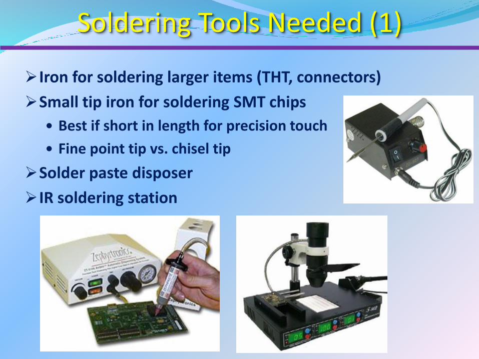
Soldering Tools Needed (1)
Iron for soldering larger items (THT, connectors)
Small tip iron for soldering SMT chips
Best if short in length for precision touch
Fine point tip vs. chisel tip
Solder paste disposer
IR soldering station

Soldering Tools Needed (2)
Cleaner: Isopropyl alcohol
Glue and toothpicks
Quality tweezers (ESD rated, stainless steel, rounded tips)
Dental picks
Flux pen – avoid flux dispensers (too messy)
Solder wire – as thin as possible
Solder paste and needles
Vise to hold your board; Fume extractor
Magnifying lamp or Visor Magnifier

Preparation Before SolderingClean milled PCB from dust, oil residues,
and oxidation
This will greatly improve solder wetting
Isopropyl alcohol and a toothbrush
Do not use acetone in the ECE lab
Remember, re-oxidation starts shortly – you only have about one hour time
Place your board in a vise
Understand how you can gain access from different directions
Understand how you can adjust vise to improve the access
Prepare the iron
Define temperature to work with (!!!)

Soldering Methods
We will discuss two classes of soldering methods, when applied to SMT devices:
1) Traditional manual hand-based methods
2) Modern semi-automated IR soldering methods
(with equipment available in the ECE Fabrication Lab.)

Manual SMT Soldering Technique 1
Using iron and solder in coordination
Process:
1) Apply flux to footprints only
2) Place (glue) chips to the PCB
3) Execute 1-2-3-4 soldering steps
Slide and point iron at pin-2-pad contact
Wait Touch with solder wire Release
Requires an extreme precision when used on small pitch multi-pin chips. It’s more suitable for SMT resistors, etc.
It’s easy for solder to spread around and join pins together
If so, do not panic and use solder-wick to remove excess solder
circuitwork.com

Manual SMD Soldering Technique 2
Using iron only – an effective technique
Process:
1) Apply flux to footprints
2) Apply solder to footprints (not too much, not too little)
Simply move iron with solder deposit through all pads
3) Inspect solder height across all pads – must be uniform
4) Clean and reapply flux
5) Place and hold/press a chip
6) Execute 1-2-3 soldering steps
Push iron down vertically on a single leg
Wait Release
YESNO

Manual Soldering Tips (1)
Do not use Technique 2 when soldering:
Chips of a block structure such as resistors, capacitors, etc.
You can easily damage copper trace and pads
Eventually, you can:
1. Apply solder on one pad only (!)
2. Solder a chip only on one side, so it will stay firm
3. Finally solder a chip on the other side
First, iron was applied here What is going to happen if you Push iron right here after the first step?
Manual Soldering Tips (2)
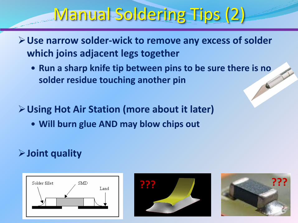
Use narrow solder-wick to remove any excess of solder which joins adjacent legs together
Run a sharp knife tip between pins to be sure there is no solder residue touching another pin
Using Hot Air Station (more about it later)
Will burn glue AND may blow chips out
Joint quality
??? ???

Modern Soldering Technique 1
Applicable to all SMDs
Process:
1) Apply flux to cleaned footprints
2) Glue (if needed) a chip to PCB (do not glue over flux residue)
3) Dispose solder paste at the edge of chip leg (dots or a line)
4) Solder using IR soldering station
5) Use a solder-wick to remove excess solderPaste line Paste dots Final resultGlue
Glue

Modern Soldering Technique 2
The same as the Technique 1, but
Dispose solder paste on footprints first, and next
Align and place a chip over
Difficult to do it precisely without spreading solder paste around
Solder paste disposed: line vs dots Chip placed and aligned
After IR soldering After excess solder removal

Modern Soldering Technique 3
Based on pre-soldering the footprints and following with IR soldering
Process:1) Apply flux to footprints
2) Apply solder to footprints (not too much, not too little)Simply wet the footprints by moving a larger iron with solder deposit through all pads
3) Inspect solder height across all pads – must be of equal height (!!!)
4) Clean and reapply flux
5) Use IR soldering station
(Optionally, push the chip down
using tweezers)
YESNO

Soldering QFN Chips
Soldering these chips is possible but requires a special technique
We soldered many of them already
Ask for help/instructions

Solder Paste Disposer
Zephyrtronics ZT-5100 instrument
Uses externally supplied compressed air (pressure up to 90psi)
Activation via a foot pedal
Parameters to work with:
Air pressure (do not exceed 70psi)
Disposal time (Use extremely small time for small diameter needles and dots)
Back suction
Test your skills first

Solder Paste Disposal Tips
Depending on your hand coordination – small dots are preferred rather than a line (!)
Small dots properly disposed give the best results
Remember: “Less is better”
Solder paste must be of room temperature
Remove from refrigerator minimum 2 hours earlier
Use small diameter needle
Practice on separate piece of cardboard
Experimentally test dispenser parameters
Touch the pad decisively – do not hold the needle above
If there is too much mess, clean the PCB and start over
Do not touch the solder paste with bare hands (!!!)
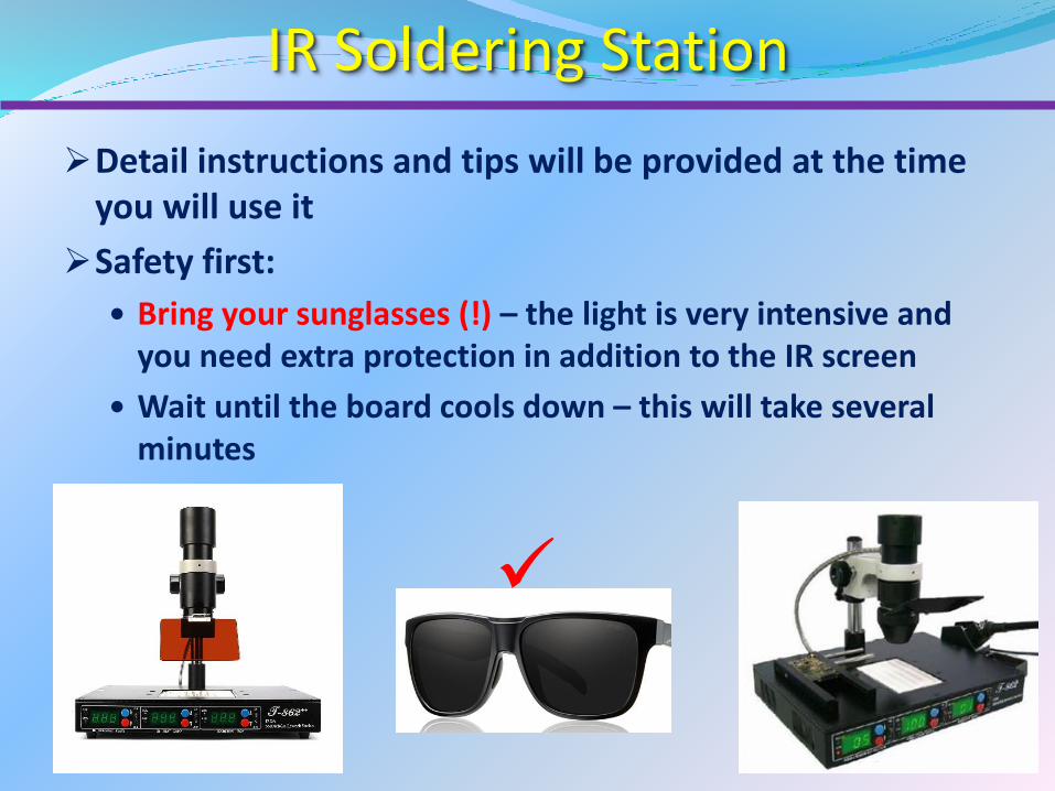
IR Soldering Station
Detail instructions and tips will be provided at the time you will use it
Safety first:
Bring your sunglasses (!) – the light is very intensive and you need extra protection in addition to the IR screen
Wait until the board cools down – this will take several minutes
More Soldering Tips (1)
Design your PCB is such a way that chip placement has a pattern suitable for easy soldering
Align all resistors, caps, etc. in one direction (maximum two) – horizontal or vertical
The same applies to multi-pin chips
In summary, have an order in chip placement on your PCB
This will speed up soldering and you will not miss joints
Watch out for placement errors (it happened to me)
Soldering should be done by one person (if you really need then second person can quietly assist)
Do not touch chips with your fingers !!!
They are already tinned
More Soldering Tips (2)
Do not overheat SMT components
Many are sensitive to heat (even resistors and capacitors)
Remove the iron immediately after smoke from the flux disappears
Approximately within 2sec after solder melts
Do not tin-plate PCB
Seriously, this is not needed for SMT PCBs
Prototype PCBs do not need tin plating anyway

Rework for SMT (1)
More difficult than soldering SMT components
Do not use excessive heat/force no matter what – remember
Copper traces are glued
Components are sensitive to excessive heat
First step: Remove solder using solder-wick (very narrow)
Second step: Use proper tool to remove entire chip
Hot Tweezers – for removal of:
Resistors, capacitors, etc.
Dual-row multi-pin chips
You need to select proper adapter,
if available

Rework for SMT (2)Hot air station – for removal of:
All-around multiple-pin chips
Dual-row multiple-pin chips
Other focused rework
Use proper adapter
IR soldering station – for removal of:
Larger chips
Non-typical chips, etc.
First, heat up PCB from bottom to 150°C
Next, use top heater to gradually increase temp
Remove a chip with thermally isolated tweezers

Rework Tools
Rework tools are available upon request or can be accessed in the ECE Fabrication Lab.
Contact Lab TA/Technician
Tools must be returned immediately
You need to babysit these tools – they are sensitive to abuse
Safety first !!!
NEVER work with hot air tool at temp >400° OR lowest air flow
You will damage this valuable station
It may melt in your hand (!)
Always use sunglasses in addition to IR screen when working with IR soldering

Questions