Embed Size (px)
Citation preview

Order this documentby AN2183/D
Fre
esc
ale
Se
mic
on
du
cto
r, I
nc
...
Semiconductor Products SectorApplication Note
AN2183
Using FLASH as EEPROM on the MC68HC908GP32By Derrick H.J. Klotz
Field Applications EngineerToronto, Canada
Introduction
This application note describes a method for using the on-chip FLASH memory of the MC68HC908GP32 as one would typically use EEPROM (electrically erasable programmable read-only memory). For the purposes of this application note, the FLASH memory that is manipulated via this method is referred to as "FlashEE." It is expected that the reader is somewhat familiar with the MC68HC908GP32/08GP32 Technical Data book, Motorola document order number MC68HC908GP32/H, as well as typical EEPROM device usage.
In many projects, EEPROMs are used as nonvolatile storage for calibration data, control information, data logging, etc. The FLASH memory technology employed in the M68HC908 Family of microcontrollers (MCU) is capable of being reprogrammed easily while the application software is executing. Project cost savings can be realized by simply using an appropriate section of the on-chip FLASH memory as one would use an off-chip EEPROM device.
© Motorola, Inc., 2001
For More Information On This Product, Go to: www.freescale.com

Application Note
F
ree
sca
le S
em
ico
nd
uc
tor,
I
Freescale Semiconductor, Inc.n
c..
.
In order to verify the correct operation of the FlashEE routines, a test program is included in this application note. This program demonstrates how these routines would be integrated into a project. The test program communicates with a host computer via a simple RS-232 connection in order to facilitate testing. User programs that include the FlashEE routines are free to implement them as one would commonly expect to use EEPROM algorithms for various forms of data storage.
FlashEE Implementation
Specifications for the M68HC908 Family FLASH memory indicate a program/erase cycle endurance of 10,000 cycles across the full operating temperature range. This is typically more than sufficient for most applications. However, this value can be mathematically elongated by the number of times a small data block can fit within a FLASH erase page.
It is important to note that the while the FLASH memory is “page” erasable, it is, in fact, byte programmable. It’s organization is configured for efficient “row” programming, but any algorithm must write each location on a byte-by-byte basis. There is no limit to the minimum number of bytes that must be programmed within a row. But every time a row is programmed, the high voltage charge pump must be enabled and disabled, regardless of the number of bytes that are programmed.
A critical FLASH memory specification is the cumulative program high voltage period. This is the maximum total time that a specific FLASH program row is subjected to being programmed between erasures. The technical data for the MC68HC908GP32 lists this maximum specification as being 4 ms.
The subroutines herein are optimized to program relatively small blocks of data sequentially within the FLASH memory, thereby minimizing the total cumulative length of time spent programming. These subroutines will only erase the FlashEE space when there is no more room for the next data block. Each FLASH erase page consists of two program rows. The FLASH erase page size for the MC68HC908GP32 is 128 bytes.
AN2183
2 For More Information On This Product,
Go to: www.freescale.com

Application NoteFlashEE Implementation
F
ree
sca
le S
em
ico
nd
uc
tor,
I
Freescale Semiconductor, Inc.n
c..
.
If an example application uses a FlashEE data block size of four bytes, then 32 program cycles of four bytes each will be performed prior to executing a single erase cycle, at which point this would be considered one complete program/erase cycle. Hence, in this example, the FlashEE endurance would be calculated as being 320,000 program/erase cycles (in other words, 10,000 x 32).
The high voltage program time used by the subroutines herein to program four bytes is less than 150 µs. Each program row would be subjected to a program cycle 16 times (remember, two program rows per erase page). This provides a cumulative time of less than 2.4 ms (150 µs x 16), which is less than the maximum specification given.
The FLASH block protect register (FLBPR) points to the first FLASH memory location to be protected. When programmed, every location from that address to $FFFF will be protected from accidental erasure. For this reason, it is easiest to assign the FlashEE sections to the very beginning of the FLASH memory, assuming that the FLBPR may be used to protect application code.
To simplify the FlashEE implementation, some essential guidelines have been used, specifically:
• FlashEE data is written in blocks of multiple bytes.
• Each FlashEE data block fits within a single FLASH program row.
• The first FlashEE data block byte to be written cannot be equal to $FF.
Programming only one byte is possible, but may result in application code inefficiencies since an entire 128-byte FLASH erase page would need to be reserved for each single byte of FlashEE.
If the data storage space requirement exceeds the size of a single FLASH program row (i.e., more than 64 bytes on the MC68HC908GP32), then the data will need to be split up over multiple FlashEE sections, each occupying one FLASH erase page (i.e., 128 bytes on the MC68HC908GP32). If multiple FlashEE sections are used, they must be manipulated separately. This is demonstrated with the test program provided.
AN2183
For More Information On This Product,
Go to: www.freescale.com

Application Note
F
ree
sca
le S
em
ico
nd
uc
tor,
I
Freescale Semiconductor, Inc.n
c..
.
As part of a search algorithm, the software interrogates the first byte location of each FlashEE data block to see if it is erased (i.e., $FF). For this reason, when writing a new block of data, the first byte must not be $FF. All subsequent data block locations have no restrictions on their stored value.
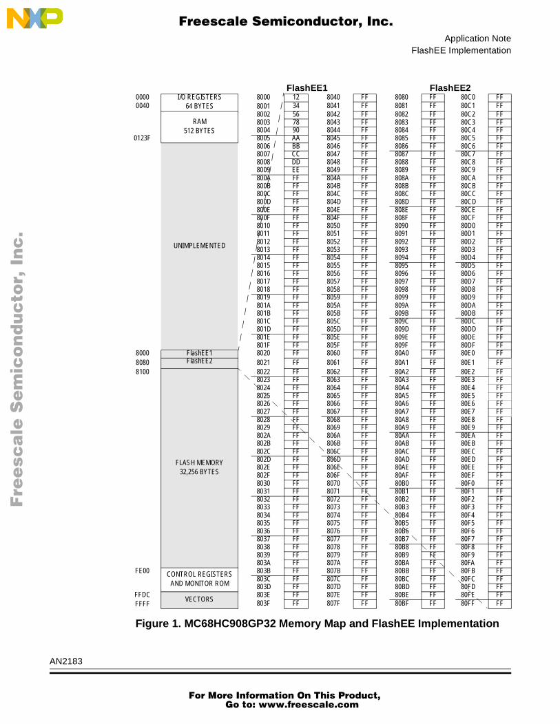
Figure 1 shows the MC68HC908GP32 memory map and the space occupied by two separate FlashEE sections (128 bytes each). Note that the erased state of the FLASH memory is $FF and that the first 10 locations ($8000 to $8009) are not erased. This represents the current state of FlashEE1 at the end of the example host test session shown in Figure 2 and described later in this text.
As defined in the example provided, FlashEE1 starts at address $8000 with a data block size of five bytes. FlashEE2 starts at address $8080 and has a data block size of seven bytes. Although reasonably obvious, delineations are shown in Figure 1 that demonstrate that neither five nor seven evenly fit into a FLASH program row that is 64 bytes in size. The routines provided will store the appropriate data sequentially in the respective FlashEE sections only up to the last complete available data block space. As defined, FlashEE1 will never store a value in the last four locations of its FLASH program row (i.e., locations $803C to $803F and $807C to $807F will always be erased.) Similarly, the last byte in each FLASH program row of FlashEE2 will also remain erased (i.e., locations $80BF and $80FF). A FlashEE section with a data block size of 33 to 64 bytes inclusive will only fit the data into each FLASH program row once, leaving the remaining locations erased.
The program files provided are:
• flashee.equ — FlashEE subroutine operational parameter definitions
• flashee.asm — FlashEE subroutines
• eetest.asm — FlashEE test program
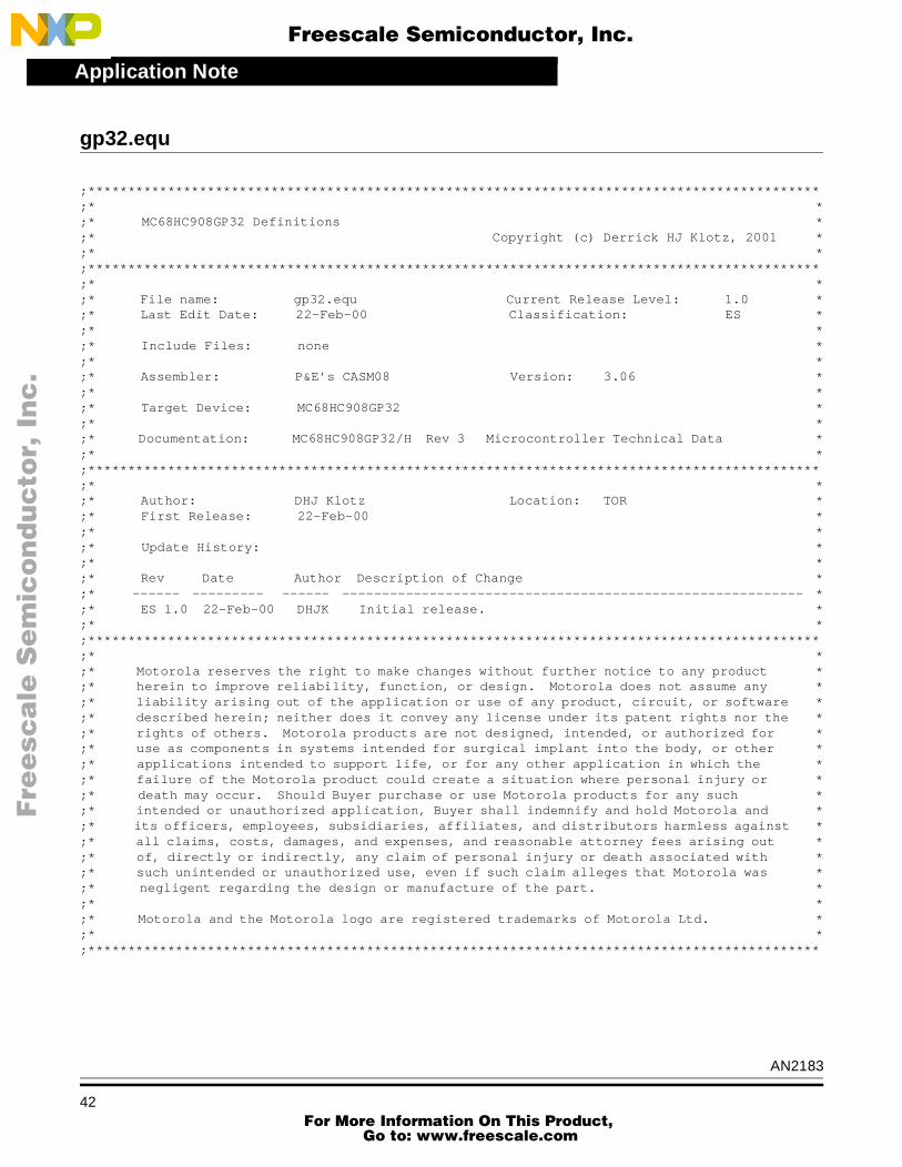
• gp32.equ — MC68HC908GP32 microcontroller definitions
AN2183
4 For More Information On This Product,
Go to: www.freescale.com
Application NoteFlashEE Implementation
F
ree
sca
le S
em
ico
nd
uc
tor,
I
Freescale Semiconductor, Inc.n
c..
.
FlashEE1 FlashEE20000 I/O REGISTERS
64 BYTES80008001
12 8040 FF 8080 FF 80C0 FF0040 34 8041 FF 8081 FF 80C1 FF
RAM 512 BYTES
8002 56 8042 FF 8082 FF 80C2 FF8003 78 8043 FF 8083 FF 80C3 FF8004 90 8044 FF 8084 FF 80C4 FF
0123F 8005 AA 8045 FF 8085 FF 80C5 FF
UNIMPLEMENTED
8006 BB 8046 FF 8086 FF 80C6 FF8007 CC 8047 FF 8087 FF 80C7 FF8008 DD 8048 FF 8088 FF 80C8 FF8009 EE 8049 FF 8089 FF 80C9 FF800A FF 804A FF 808A FF 80CA FF800B FF 804B FF 808B FF 80CB FF800C FF 804C FF 808C FF 80CC FF800D FF 804D FF 808D FF 80CD FF800E FF 804E FF 808E FF 80CE FF800F FF 804F FF 808F FF 80CF FF8010 FF 8050 FF 8090 FF 80D0 FF8011 FF 8051 FF 8091 FF 80D1 FF8012 FF 8052 FF 8092 FF 80D2 FF8013 FF 8053 FF 8093 FF 80D3 FF8014 FF 8054 FF 8094 FF 80D4 FF8015 FF 8055 FF 8095 FF 80D5 FF8016 FF 8056 FF 8096 FF 80D6 FF8017 FF 8057 FF 8097 FF 80D7 FF8018 FF 8058 FF 8098 FF 80D8 FF8019 FF 8059 FF 8099 FF 80D9 FF801A FF 805A FF 809A FF 80DA FF801B FF 805B FF 809B FF 80DB FF801C FF 805C FF 809C FF 80DC FF801D FF 805D FF 809D FF 80DD FF801E FF 805E FF 809E FF 80DE FF801F FF 805F FF 809F FF 80DF FF
8000 FlashEE1 8020 FF 8060 FF 80A0 FF 80E0 FF8080 FlashEE2 8021 FF 8061 FF 80A1 FF 80E1 FF8100
FLASH MEMORY32,256 BYTES
8022 FF 8062 FF 80A2 FF 80E2 FF8023 FF 8063 FF 80A3 FF 80E3 FF8024 FF 8064 FF 80A4 FF 80E4 FF8025 FF 8065 FF 80A5 FF 80E5 FF8026 FF 8066 FF 80A6 FF 80E6 FF8027 FF 8067 FF 80A7 FF 80E7 FF8028 FF 8068 FF 80A8 FF 80E8 FF8029 FF 8069 FF 80A9 FF 80E9 FF802A FF 806A FF 80AA FF 80EA FF802B FF 806B FF 80AB FF 80EB FF802C FF 806C FF 80AC FF 80EC FF802D FF 806D FF 80AD FF 80ED FF802E FF 806E FF 80AE FF 80EE FF802F FF 806F FF 80AF FF 80EF FF8030 FF 8070 FF 80B0 FF 80F0 FF8031 FF 8071 FF 80B1 FF 80F1 FF8032 FF 8072 FF 80B2 FF 80F2 FF8033 FF 8073 FF 80B3 FF 80F3 FF8034 FF 8074 FF 80B4 FF 80F4 FF8035 FF 8075 FF 80B5 FF 80F5 FF8036 FF 8076 FF 80B6 FF 80F6 FF8037 FF 8077 FF 80B7 FF 80F7 FF8038 FF 8078 FF 80B8 FF 80F8 FF8039 FF 8079 FF 80B9 FF 80F9 FF803A FF 807A FF 80BA FF 80FA FF
FE00 CONTROL REGISTERSAND MONITOR ROM
803B FF 807B FF 80BB FF 80FB FF803C FF 807C FF 80BC FF 80FC FF803D FF 807D FF 80BD FF 80FD FF
FFDCFFFF
VECTORS803E FF 807E FF 80BE FF 80FE FF803F FF 807F FF 80BF FF 80FF FF
Figure 1. MC68HC908GP32 Memory Map and FlashEE Implementation
AN2183
For More Information On This Product,
Go to: www.freescale.com

Application Note
F
ree
sca
le S
em
ico
nd
uc
tor,
I
Freescale Semiconductor, Inc.n
c..
.
flashee.equ Subroutines
The FlashEE subroutines are tailored to the needs and operation conditions of a specific application by modifying the parameters provided in this file, which must be included near the top of the application program file. To help avoid assembly language label naming conflicts, all labels used in this file start with either "EE" or "Ram".
The parameters defined are grouped into three specific categories:
• Microcontroller FLASH memory parameters
• FlashEE data parameters
• Microcontroller bus frequency parameters
Microcontroller FLASH Memory Parameters
The specific sizes of the FLASH memory program row and erase page are defined here (64 bytes and 128 bytes, respectively, for the MC68HC908GP32). Also, the erased state of a FLASH byte is also declared as $FF.
These parameters are initially defined as:
EE_FlashPage: equ 128EE_FlashRow: equ 64EE_FlashErased: equ $FF
FlashEE Data Parameters
The starting address of each FlashEE section is declared here. These parameters are not directly used by the FlashEE subroutines. They are passed forward by the application program when these subroutines are called. For demonstration purposes, two separate FlashEE sections are shown, although many more are possible.
The size of each FlashEE data block is also defined. Note that each FlashEE section can have its own unique data block size.
AN2183
6 For More Information On This Product,
Go to: www.freescale.com

Application Noteflashee.asm Subroutines
F
ree
sca
le S
em
ico
nd
uc
tor,
I
Freescale Semiconductor, Inc.n
c..
.
The parameters for FlashEE1 are initially defined as:
EE_StartAddr1: equ $8000EE_BlockSize1: equ 5
The parameters for FlashEE2 are initially defined as:
EE_StartAddr2: equ {EE_StartAddr2+EE_FlashPage}EE_BlockSize2: equ 7
Note that the assembler will assign the label "EE_StartAddr2" with a value of $8080.
Microcontroller Bus Frequency Parameters
The FlashEE subroutines employ delay loops that must be tuned to the microcontroller bus frequency. The values for these parameters for a bus frequency of 7.3728 MHz are provided in the software listing. If a different bus frequency is desired, then these parameters must be changed in accordance with the formula provided, specifically:
Value = ((delay in µs) x (bus frequency in MHz) – 2) ÷ 3
As an example, a delay of 30 µs with a bus frequency of 7.3728 MHz would result in the following:
RamDelay30 = ((30) x (7.3728) – 2) ÷ 3 = 73.06 ≅ 74
For a 7.3728-MHz bus frequency, the required parameters are initially defined as:
RamDelay5: equ 12RamDelay10: equ 24RamDelay30: equ 74RamDelay50: equ 122
flashee.asm Subroutines
This file contains the FlashEE subroutine source code and must be included in the application program file. These subroutines only use local variables on the stack and, hence, do not require any other predefined global variable space resources. The maximum available stack space
AN2183
For More Information On This Product,
Go to: www.freescale.com

Application Note
F
ree
sca
le S
em
ico
nd
uc
tor,
I
Freescale Semiconductor, Inc.n
c..
.
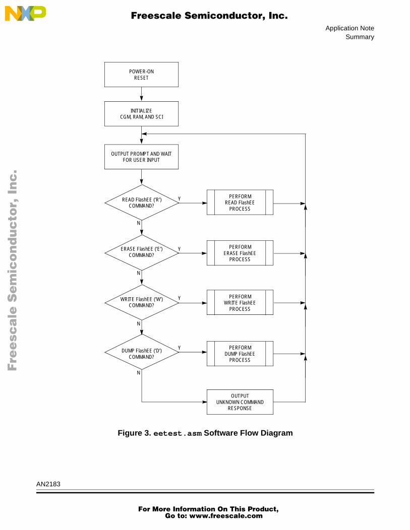
requirement is 80 bytes. To help avoid assembly language label naming conflicts, all labels used start with either "EE" or "Ram". The flow diagrams of these routines (with the exception of the Dump utility, due to its simplicity) are provided in Figure 3 through Figure 8.
The available FlashEE routines are:
• EERead — Read the current valid FlashEE data block
• EEErase — Erase an entire FlashEE section
• EEWrite — Write a new FlashEE data block
EERead This subroutine is called with the 16-bit index register H:X pointing at the starting address of the desired FlashEE section and the accumulator preloaded with that FlashEE section’s data block size. The FlashEE section is sequentially scanned, block by block, until an erased FLASH byte (i.e., $FF) is found occupying the first location of a data block or the end of the section is reached.
This subroutine returns with the 16-bit index register H:X pointing to the first location of the most recent FlashEE data block and the data in that location stored in the accumulator. The calling routine should check the accumulator value for $FF to see if any data has been stored in the FlashEE. Refer to Check_Read subroutine in the eetest.asm. This check should only be needed when an EERead is performed before the very first EEWrite.
EEErase This subroutine is used to erase the contents of a FlashEE section. It is called with the 16-bit index register H:X pointing at the starting address of the desired FlashEE section. The value in H:X is returned unchanged. Regardless of bus frequency, this subroutine will execute in just over one millisecond. (Specifically, at a bus frequency of 7.3728 MHz, this subroutine executes in about 1096 µs.)
Note that this subroutine will copy and execute a program in RAM. This is required due to the fact that erasing FLASH locations cannot be performed by code being executed from the FLASH memory. While executing code from RAM, all interrupts are disabled.
AN2183
8 For More Information On This Product,
Go to: www.freescale.com

Application Noteeetest.asm Subroutines
F
ree
sca
le S
em
ico
nd
uc
tor,
I
Freescale Semiconductor, Inc.n
c..
.
EEWrite This subroutine requires two address pointers when called. The 16-bit starting address of the desired FlashEE section must be saved on the stack just prior to calling this subroutine. In addition, the 16-bit index register H:X must point to the first byte of a source data block, which is typically a buffer located in RAM. As well, the accumulator is preloaded with the FlashEE data block size. This subroutine will then copy the required number of bytes sequentially from the source location into the FlashEE.
As a point of reference toward understanding the speed of this subroutine, consider using a data block of 16 bytes and a bus frequency of 7.3728 MHz. The best case programming time would be about 644 µs. The worst case would involve writing the data block into the FlashEE with no available room. This requires that the FlashEE first be erased prior to programming the data. In this given scenario, this subroutine executes in about 1772 µs, of which just over 1000 µs is due to the FlashEE erasure procedure.
Note that this subroutine will copy and execute a program in RAM. This is required due to the fact that programming FLASH locations cannot be performed by code being executed from the FLASH memory. While executing code from RAM, all interrupts are disabled.
eetest.asm Subroutines
This file provides an executable demo program used to test and verify the use of the FlashEE subroutines and files. Note that the files flashee.equ, flashee.asm, and gp32.equ are incorporated in this test program via the "include" assembler directive.
A simple user interface is provided via the on-chip serial communications interface (SCI) and industry standard RS232 communications with a host computer executing a simple terminal program. The serial bit rate is configured for 115.2 kbaud.
The software implements four single ASCII character commands (case insensitive) and provides the ability to test and interrogate two separate
AN2183
For More Information On This Product,
Go to: www.freescale.com
Application Note
F
ree
sca
le S
em
ico
nd
uc
tor,
I
Freescale Semiconductor, Inc.n
c..
.
FlashEE sections. Each command is followed by either "1" or "2" to indicate the desired FlashEE section.
The commands are:
• R — Read FlashEE
• E — Erase FlashEE
• W — Write FlashEE
• D — Dump FlashEE
An example of the host terminal display during a simple test session using FlashEE1 with a block size of five bytes is shown in Figure 2. The program implements a default prompt to the user of FlashEE>.
The first user command is d1, or "dump the contents of FlashEE1." All 128 bytes are printed out in a format that is relatively easy to read. Note that at this point, the entire FlashEE section is erased (i.e., all locations contain $FF). The second command issued is r1, or "read the most recent FlashEE1 data block." Since FlashEE1 is erased, a message is sent indicating that no data is currently stored in FlashEE1.
Next, the user has requested that a block of data be written into FlashEE1 with w1. The program responds with an equal sign (=) and then accepts the correct number of hexadecimal values (five in total for FlashEE1). The user verifies that the data has been programmed correctly by first using the r1 command, and secondly with d1 which clearly indicates where the data has been stored.
The user enters another block of data with the next w1 command. The following d1 entry shows that the new data has been correctly stored in the next data block location. And the next r1 command confirms that the read subroutine correctly identifies which is the most recent data.
Continuing with this method, the demo program provided was used to test and verify the correct operation of the FlashEE subroutines.
AN2183
10 For More Information On This Product,
Go to: www.freescale.com

Application Noteeetest.asm Subroutines
F
ree
sca
le S
em
ico
nd
uc
tor,
I
Freescale Semiconductor, Inc.n
c..
.
Figure 2. Simple Host Terminal Test Session Display
Read FlashEE (R) After entering the single character R, followed by either "1" or "2", the program will respond by outputting the most recent data byte block. In the example shown, the first time R is entered and the FlashEE is erased as indicated by the software’s response. Subsequent examples show the current data block data being reported back to the host.
Erase FlashEE (E) This command will directly execute the EEErase subroutine and erase the selected FlashEE section.
FlashEE>d1 FF FF FF FF FF FF FF FF FF FF FF FF FF FF FF FF FF FF FF FF FF FF FF FF FF FF FF FF FF FF FF FF FF FF FF FF FF FF FF FF FF FF FF FF FF FF FF FF FF FF FF FF FF FF FF FF FF FF FF FF FF FF FF FF FF FF FF FF FF FF FF FF FF FF FF FF FF FF FF FF FF FF FF FF FF FF FF FF FF FF FF FF FF FF FF FF FF FF FF FF FF FF FF FF FF FF FF FF FF FF FF FFFlashEE>r1 FlashEE erasedFlashEE>w1=12 34 56 78 90FlashEE>r1 12 34 56 78 90FlashEE>d1 12 34 56 78 90 FF FF FF FF FF FF FF FF FF FF FF FF FF FF FF FF FF FF FF FF FF FF FF FF FF FF FF FF FF FF FF FF FF FF FF FF FF FF FF FF FF FF FF FF FF FF FF FF FF FF FF FF FF FF FF FF FF FF FF FF FF FF FF FF FF FF FF FF FF FF FF FF FF FF FF FF FF FF FF FF FF FF FF FF FF FF FF FF FF FF FF FF FF FF FF FF FF FF FF FF FF FF FF FF FF FF FF FF FF FF FF FF FF FF FF FF FF FF FF FF FF FF FFFlashEE>w1= aa bb cc dd eeFlashEE>d1 12 34 56 78 90 AA BB CC DD EE FF FF FF FF FF FF FF FF FF FF FF FF FF FF FF FF FF FF FF FF FF FF FF FF FF FF FF FF FF FF FF FF FF FF FF FF FF FF FF FF FF FF FF FF FF FF FF FF FF FF FF FF FF FF FF FF FF FF FF FF FF FF FF FF FF FF FF FF FF FF FF FF FF FF FF FF FF FF FF FF FF FF FF FF FF FF FF FF FF FF FF FF FF FF FF FF FF FF FF FF FF FF FF FF FF FF FF FF FF FF FF FF FF FF FF FF FF FFFlashEE>r1 AA BB CC DD EEFlashEE>_
AN2183
For More Information On This Product,
Go to: www.freescale.com

Application Note
F
ree
sca
le S
em
ico
nd
uc
tor,
I
Freescale Semiconductor, Inc.n
c..
.
Write FlashEE (W) After entering the single character W, followed by either "1" or "2", the program will respond by prompting the user to enter a data block string of data. Each entry must be a valid hexadecimal value and is echoed back as typed. Entering a non-hexadecimal value results in the process being stopped with the default prompt being output. After entering the required number of bytes, the FlashEE is programmed with the data provided.
Dump FlashEE (D) This command will output the current contents of the selected FlashEE section.
Summary
Most projects using the M68HC908 Family of microcontrollers requiring nonvolatile data storage that is application software programmable need not incur the added cost of external EEPROM devices. A method for using the on-chip FLASH memory for such application purposes has been demonstrated with this application note.
AN2183
12 For More Information On This Product,
Go to: www.freescale.com
Application NoteSummary
F
ree
sca
le S
em
ico
nd
uc
tor,
I
Freescale Semiconductor, Inc.n
c..
.
Figure 3. eetest.asm Software Flow Diagram
POWER-ONRESET
INITIALIZECGM, RAM, AND SCI
OUTPUT PROMPT AND WAITFOR USER INPUT
PERFORMREAD FlashEE
PROCESS
READ FlashEE (’R’)COMMAND?
ERASE FlashEE (’E’)COMMAND?
WRITE FlashEE (’W’)COMMAND?
DUMP FlashEE (’D’)COMMAND?
OUTPUTUNKNOWN COMMAND
RESPONSE
PERFORMERASE FlashEE
PROCESS
PERFORMWRITE FlashEE
PROCESS
PERFORMDUMP FlashEE
PROCESS
Y
Y
Y
Y
N
N
N
N
AN2183
For More Information On This Product,
Go to: www.freescale.com

Application Note
F
ree
sca
le S
em
ico
nd
uc
tor,
I
Freescale Semiconductor, Inc.n
c..
.
Figure 4. Read FlashEE Software Flow Diagram
Y
N
PERFORM FIND FIRSTERASED FLASH
LOCATION PROCESS
PERFORMREAD FlashEE
PROCESS
IS FIRST LOCATIONOF FIRST ROW
ERASED?
IS THEREROOM FOR ANOTHER
DATA BLOCK?
SAVE CURRENTLOCATION POINTER
TEMPORARILY
ADVANCE LOCATION POINTERTO START OF
SECOND PROGRAM ROW
IS FIRST LOCATIONOF SECOND ROW
ERASED?
PERFORM FIND FIRSTERASED FLASH
LOCATION PROCESS
ADJUST LOCATION POINTERBACK ONE
DATA BLOCK SIZE
RETURN WITHFIRST DATA BYTE
FROM BLOCK
RESTORE PREVIOUSLOCATION POINTER
Y
Y
N
N
EXITPROCESS
AN2183
14 For More Information On This Product,
Go to: www.freescale.com

Application NoteSummary
F
ree
sca
le S
em
ico
nd
uc
tor,
I
Freescale Semiconductor, Inc.n
c..
.
Figure 5. Erase FlashEE Software Flow Diagrams
COPYERASE FLASH ROUTINE
ONTO STACK
PERFORMERASE FlashEE
PROCESS
SAVECONDITION CODE REGISTERAND DISABLE INTERRUPTS
EXECUTEERASE FLASH ROUTINE
IN RAM
RESTORECONDITION CODE REGISTER
RETURN WITHFlashEE PAGE EXIT
PROCESSLOCATION POINTER
SET ERASE BIT IN FLCR,READ FLBPR
AND WRITE TO POINTED PAGE
EXECUTEERASE FLASH ROUTINE
IN RAM
WAIT > 10 µs,SET HVEN BIT IN FLCR
AND WAIT > 1 ms
CLEAR ERASE BITIN FLCR
AND WAIT > 5 µs,
CLEAR HVEN BIT IN FLCRAND WAIT > 1 µs,
EXITPROCESS
AN2183
For More Information On This Product,
Go to: www.freescale.com

Application Note
F
ree
sca
le S
em
ico
nd
uc
tor,
I
Freescale Semiconductor, Inc.n
c..
.
Figure 6. Write FlashEE Software Flow Diagram
Y
N
PERFORM FIND FIRSTERASED FLASH
LOCATION PROCESS
PERFORMWRITE FlashEE
PROCESS
IS THEREROOM FOR ANOTHER
DATA BLOCK?
ADVANCE LOCATION POINTERTO START OF
SECOND PROGRAM ROW
IS THEREROOM FOR ANOTHER
DATA BLOCK?
PERFORMERASED FlashEE
PROCESS
COPYPROGRAM FLASH ROUTINE
ONTO STACK
SAVECONDITION CODE REGISTER
AND DISABLEINTERRUPTS
PREPAREBLOCK SIZE COUNTER
Y
N
EXITPROCESS
PERFORM FIND FIRSTERASED FLASH
LOCATION PROCESS
PREPARESOURCE AND DESTINATION
POINTERS
EXECUTEPROGRAM FLASHROUTINE IN RAM
RESTORECONDITION CODE REGISTER
AN2183
16 For More Information On This Product,
Go to: www.freescale.com

Application NoteSummary
F
ree
sca
le S
em
ico
nd
uc
tor,
I
Freescale Semiconductor, Inc.n
c..
.
Figure 7. Write FlashEE RAM Routine Software Flow Diagram
Y
N
SET PGM BIT IN FLCR,READ FLBPR
AND WRITE TO POINTED PAGE
EXECUTEPROGRAM FLASHROUTINE IN RAM
COPY DATA BYTE FROMSOURCE TO DESTINATION
AND WAIT 30-40 µs
IS BLOCK SIZE COUNTER
ZERO?
EXITPROCESS
WAIT > 10 µs,SET HVEN BIT IN FLCR
AND WAIT > 5 µs
ADVANCESOURCE AND DESTINATION
POINTERS
DECREMENTBLOCK SIZECOUNTER
CLEAR PGM BITIN FLCR
AND WAIT > 5 µs
CLEAR HVEN BITIN FLCR
AND WAIT > 1 µs
AN2183
For More Information On This Product,
Go to: www.freescale.com

Application Note
F
ree
sca
le S
em
ico
nd
uc
tor,
I
Freescale Semiconductor, Inc.n
c..
.
Figure 8. Find First Erased FlashEE Data Block Software Flow Diagram
Y
N
INITIALIZEBLOCK COUNTER
PERFORM FIND FIRSTERASED FLASH
LOCATION PROCESS
IS CURRENTLOCATIONERASED?
EXITPROCESS
SUBTRACT BLOCK SIZEFROM BLOCK COUNTER
IS BLOCKCOUNTER
NEGATIVE?
N
Y RETURN WITHBLOCK COUNTER
ADVANCELOCATION POINTER
AN2183
18 For More Information On This Product,
Go to: www.freescale.com

Application Noteflashee.equ
F
ree
sca
le S
em
ico
nd
uc
tor,
I
Freescale Semiconductor, Inc.n
c..
.
flashee.equ
;********************************************************************************************;* *;* Flash as EEPROM - MC68HC908GP32 *;* Copyright (c) Motorola, 2001 *;* *;********************************************************************************************;* *;* This file provides the application specific parameters for the FlashEE routines. *;* This program has been specially tailored towards the MC68HC908GP32. *;* *;********************************************************************************************;* *;* File name: flashee.equ Current Release Level: 1.0 *;* Last Edit Date: 15-Jun-01 Classification: ES *;* *;* Include Files: gp32.equ : MC68HC908GP32 MCU definitions *;* *;* Assembler: P&E’s CASM08Z Version: 3.16 *;* *;* Target: MC68HC908GP32 *;* *;* Documentation: MC68HC908GP32/H Rev 3 *;* Motorola Microcontroller Technical Data *;* *;********************************************************************************************;* *;* Author: DHJ Klotz *;* First Release: 15-Jun-01 *;* *;* Update History: *;* *;* Rev Date Author Description of Change *;* ------ --------- ------ ----------------------------------------------------------- *;* ES 1.0 15-Jun-01 DHJK Initial release. *;* *;********************************************************************************************;* *;* Notes: *;* - This file is intended to be included within another source program along with *;* the program file "flashee.asm". All labels used in this file start with either *;* "EE" or "Ram". *;* *;* - The "FlashEE Data Parameters" and "Microcontroller Bus Frequency Parameters" *;* declared at the start of this listing must be tailored to the specific needs of *;* the target application prior to using the programs herein. *;* *;********************************************************************************************;* *;* Motorola reserves the right to make changes without further notice to any product *;* herein to improve reliability, function, or design. Motorola does not assume any *;* liability arising out of the application or use of any product, circuit, or software *;* described herein; neither does it convey any license under its patent rights nor the *;* rights of others. Motorola products are not designed, intended, or authorized for *
AN2183
For More Information On This Product,
Go to: www.freescale.com

Application Note
F
ree
sca
le S
em
ico
nd
uc
tor,
I
Freescale Semiconductor, Inc.n
c..
.
;* use as components in systems intended for surgical implant into the body, or other *;* applications intended to support life, or for any other application in which the *;* failure of the Motorola product could create a situation where personal injury or *;* death may occur. Should Buyer purchase or use Motorola products for any such *;* intended or unauthorized application, Buyer shall indemnify and hold Motorola and *;* its officers, employees, subsidiaries, affiliates, and distributors harmless against *;* all claims, costs, damages, and expenses, and reasonable attorney fees arising out *;* of, directly or indirectly, any claim of personal injury or death associated with *;* such unintended or unauthorized use, even if such claim alleges that Motorola was *;* negligent regarding the design or manufacture of the part. *;* *;* Motorola and the Motorola logo are registered trademarks of Motorola Ltd. *;* *;********************************************************************************************
;* Mircontroller FLASH Memory Parameters **************************************************;*;* These parameters reflect the specific FLASH memory characteristics of the MC68HC908GP32.;* The FlashEE software can be easily ported to other MC68HC908 family members by changing;* the parameters listed here.;*EE_FlashPage: equ 128 ; Flash Erase Page sizeEE_FlashRow: equ 64 ; Flash Program Row sizeEE_FlashErased: equ $FF ; Flash erased state
;* FlashEE Data Parameters ****************************************************************;*;* By default, the very first Flasherase page is assigned for FlashEE usage, so that the;* rest of the Flash memory can be protected via the Flash Block Protect Register (FLBPR).;*EE_StartAddr1: equ $8000 ; starting address of 1st FlashEEEE_StartAddr2: equ {EE_StartAddr1+EE_FlashPage} ; starting address of 2nd FlashEE;*;*;* The data block size for each FlashEE section is defined here. Each must be less than or;* equal to "EE_FlashRow";*EE_BlockSize1: equ 5 ; data block size for 1st FlashEE EE_BlockSize2: equ 7 ; data block size for 2nd FlashEE
;* Microcontroller Bus Frequency Parameters ***********************************************;*;* Software delay loops are initially calculated for a 7.3728 MHz bus frequency. For other;* frequencies, the following parameters must be modified accordingly.;*;* Microsecond delay parameter calculation is ((N x bus clock) - 2) / 3;* For example,;* if bus = 7.3728 MHz, then 10us -> ((10us x 7372800 - 2)) / 3 = 23.9 = 24;*;* As a check, use ((M x 3) +2) / bus clock;* For example,;* if bus = 7.3728 MHz, then for N = 24 -> ((24 x 3) + 2) / 7372800 = 10us;*RamDelay5: equ 12 ; 5us delay parameterRamDelay10: equ 24 ; 10us delay parameterRamDelay30: equ 74 ; 30us delay parameterRamDelay50: equ 122 ; 50us delay parameter
AN2183
20 For More Information On This Product,
Go to: www.freescale.com

Application Noteflashee.asm
F
ree
sca
le S
em
ico
nd
uc
tor,
I
Freescale Semiconductor, Inc.n
c..
.
flashee.asm
;********************************************************************************************;* *;* Flash as EEPROM - MC68HC908GP32 *;* Copyright (c) Motorola, 2001 *;* *;********************************************************************************************;* *;* This file provides the low level assembly routines for using the Flash as EEPROM. *;* This program has been specially tailored towards the MC68HC908GP32. *;* *;********************************************************************************************;* *;* File name: flashee.asm Current Release Level: 1.0 *;* Last Edit Date: 15-Jun-01 Classification: ES *;* *;* Include Files: gp32.equ : MC68HC908GP32 MCU definitions *;* flashee.equ : FlashEE parameters *;* *;* Assembler: P&E’s CASM08Z Version: 3.16 *;* *;* Target: MC68HC908GP32 *;* *;* Documentation: MC68HC908GP32/H Rev 3 *;* Motorola Microcontroller Technical Data *;* *;********************************************************************************************;* *;* Author: DHJ Klotz *;* First Release: 15-Jun-01 *;* *;* Update History: *;* *;* Rev Date Author Description of Change *;* ------ --------- ------ ----------------------------------------------------------- *;* ES 1.0 15-Jun-01 DHJK Initial release. *;* *;********************************************************************************************;* *;* Notes: *;* - This file is intended to be included within another source program along with *;* the FlashEE parameter file "flashee.equ". All labels used in this file start with *;* either "EE" or "Ram". *;* *;* - The "FlashEE Data Parameters" and "Microcontroller Bus Frequency Parameters" *;* declared in the include file "flashee.equ" must be tailored to the specific needs *;* of the target application prior to using the programs herein. *;* *;* - Callable subroutines are: *;* EERead : returns with H:X pointing to first FlashEE data block entry *;* EEWrite : programs FlashEE with data block pointed to by H:X *;* EEErase : erases entire FlashEE space pointed to by H:X *;* *
AN2183
For More Information On This Product,
Go to: www.freescale.com

Application Note
F
ree
sca
le S
em
ico
nd
uc
tor,
I
Freescale Semiconductor, Inc.n
c..
.
;********************************************************************************************;* *;* Motorola reserves the right to make changes without further notice to any product *;* herein to improve reliability, function, or design. Motorola does not assume any *;* liability arising out of the application or use of any product, circuit, or software *;* described herein; neither does it convey any license under its patent rights nor the *;* rights of others. Motorola products are not designed, intended, or authorized for *;* use as components in systems intended for surgical implant into the body, or other *;* applications intended to support life, or for any other application in which the *;* failure of the Motorola product could create a situation where personal injury or *;* death may occur. Should Buyer purchase or use Motorola products for any such *;* intended or unauthorized application, Buyer shall indemnify and hold Motorola and *;* its officers, employees, subsidiaries, affiliates, and distributors harmless against *;* all claims, costs, damages, and expenses, and reasonable attorney fees arising out *;* of, directly or indirectly, any claim of personal injury or death associated with *;* such unintended or unauthorized use, even if such claim alleges that Motorola was *;* negligent regarding the design or manufacture of the part. *;* *;* Motorola and the Motorola logo are registered trademarks of Motorola Ltd. *;* *;********************************************************************************************
;* Read FlashEE Block Subroutine ==========================================================;*;* This subroutine expects H:X to be pointing to the first FlashEE page location and returns;* with H:X pointing to the most recent FlashEE data. The FlashEE data block size is passed;* forward in ACC.;*;* Calling convention:;*;* ldhx #EE_StartAddr;* lda #EE_BlockSize;* jsr EERead;*;* Returns: H:X -> FlashEE block address;* ACC = first FlashEE data byte;*;* Changes: everything;*EERead:;; Find first erased location within FlashEE page.;; Check for room within first FlashEE row.; If the entire row is erased, then return with H:X unchanged. If the next available; erased FlashEE block is within the first program row, then return pointing to the; block just before it.; psha ; save FlashEE data block size pshx ; save FlashEE address lsb on stack bsr EEFindFirst ; go find next free location cpx 1,sp ; check if start of 1st row is 1st blank location beq EERead3 ; exit if so cmp 2,sp ; check if there’s room for another data block bpl EERead2 ; exit if so;; Check for room within second FlashEE row.
AN2183
22 For More Information On This Product,
Go to: www.freescale.com

Application Noteflashee.asm
F
ree
sca
le S
em
ico
nd
uc
tor,
I
Freescale Semiconductor, Inc.n
c..
.
; If the second row is erased, then return pointing to the last block in the first row.; Otherwise, return pointing to the last used block in the second row.; txa ; save current address lsb pulx ; restore FlashEE address lsb aix #EE_FlashRow ; H:X now points to second program row psha ; save previous address lsb on stack lda ,x ; check if first location cmp #EE_FlashErased ; is erased bne EERead1 ; skip if so pulx ; else, restore previous FlashEE address lsb pshx ; put back on stack for clean exit bra EERead2 ; and exitEERead1: lda 2,sp ; get FlashEE data block size bsr EEFindFirst ; go find next free locationEERead2: txa ; perform sub 2,sp ; 16-bit subtraction tax ; in order pshh ; to adjust pula ; FlashEE pointer sbc #0 ; backwards psha ; one data block pulh ; sizeEERead3: ais #2 ; deallocate stack usage lda ,x ; get first FlashEE data byte rts ; return
;* RAM Executable FlashEE Page Erase Subroutine ===========================================;*;* This subroutine will erase the Flash memory page that is being pointed to by H:X.;* This subroutine is copied into and executed from RAM and expects to be called via;* "jsr ,x".;*RamEraseEE:;; Retrieve page address.; psha ; save previous CCR on stack lda {RamEraseSize},x ; get msb ldx {RamEraseSize+1},x ; and lsb of address psha ; put msb pulh ; into HREG;; Step 1:; Set ERASE, read the Flash Block Protect Register and write any data into Flash page.; lda #{ERASE} ; set ERASE control bit sta flcr ; in Flash Control Register lda flbpr ; read from Flash Block Protect Register sta ,x ; write any data to address within page;
AN2183
For More Information On This Product,
Go to: www.freescale.com

Application Note
F
ree
sca
le S
em
ico
nd
uc
tor,
I
Freescale Semiconductor, Inc.n
c..
.
; Step 2:; Wait for >10us, then set HVEN.; lda #RamDelay10 ; wait dbnza * ; for 10us lda #{ERASE | HVEN} ; set HVEN control bit sta flcr ; in Flash Control Register;; Step 3:; Wait for >1ms, then clear ERASE.; ldx #20 ; outer loopRamEraseEE1: ; set for 20x lda #RamDelay50 ; inner loop dbnza * ; set for 50us dbnzx RamEraseEE1 ; loop back until done lda #{HVEN} ; clear ERASE control bits sta flcr ; in Flash Control Register;; Step 4:; Wait for >5us, then clear HVEN, then wait >1us and return.; lda #RamDelay5 ; wait dbnza * ; for 5us clra ; clear HVEN control bit sta flcr ; in Flash Control Register pula ; retreive previous CCR brn * ; wait for at least 1us before rts ; returning
RamEraseSize: equ {*-RamEraseEE}
;* FlashEE Page Erase Subroutine ==========================================================;*;* This subroutine will erase the Flash memory page that is being pointed to by H:X.;* 60 bytes of stack space is used, including this subroutine’s call return address.;*;* Calling convention:;*;* ldhx #EE_StartAddr;* jsr EEErase;*;* Returns: H:X unchanged;*;* Changes: ACC;*EEErase: pshx ; save pointer pshh ; on stack;; Copy FlashEE page erase routine into RAM; ldhx #RamEraseSize ; initialize pointer
AN2183
24 For More Information On This Product,
Go to: www.freescale.com

Application Noteflashee.asm
F
ree
sca
le S
em
ico
nd
uc
tor,
I
Freescale Semiconductor, Inc.n
c..
.
EEErase1: lda RamEraseEE-1,x ; get program from Flash psha ; copy into Stack dbnzx EEErase1 ; decrement pointer and loop back until done;; Execute program routine in RAM.; tsx ; use H:X to point to RAM executable routine tpa ; get CCR sei ; disable all interrupts jsr ,x ; erase Flash page; ais #RamEraseSize ; deallocate stack space used pulh ; restore pulx ; address pointer tap ; restore previous CCR rts ; return
;* Find First Erased FlashEE Location Subroutine ==========================================;*;* This subroutine is used to find the first erased FlashEE block, starting at the;* address being pointed to by H:X. The FlashEE data block size is passed forward in ACC.;*;* Calling convention:;*;* ldhx #address;* lda #EE_BlockSize;* jsr EEFindFirst;*;* Returns: H:X -> first erased FlashEE block address;* ACC = number of erased FlashEE bytes left;* CCRZ = set if erased location successfully found, otherwise clear;*;* Changes: everything;*EEFindFirst: psha ; save FlashEE data block size lda #EE_FlashRow ; get Flash Program Row size psha ; save on stack as a counterEEFindFirst1: lda #EE_FlashErased ; get erased Flash data cmp ,x ; check if Flash location is erased beq EEFindFirst2 ; exit if so pula ; else, get counter sub 1,sp ; adjust by subtracting block size bmi EEFindFirst3 ; exit if out of room psha ; else, save new count txa ; perform add 2,sp ; 16-bit addition tax ; in order pshh ; to advance pula ; FlashEE pointer adc #0 ; forwards psha ; to the pulh ; next block bra EEFindFirst1 ; loop back
AN2183
For More Information On This Product,
Go to: www.freescale.com

Application Note
F
ree
sca
le S
em
ico
nd
uc
tor,
I
Freescale Semiconductor, Inc.n
c..
.
EEFindFirst2: pula ; retrieve remaining erased bytes countEEFindFirst3: ais #1 ; deallocate stack usage rts ; return
;* FlashEE Block Program Subroutine =======================================================;*;* This subroutine will write the block of data being pointed to by H:X into the FlashEE.;* 80 bytes of stack space is used, including this subroutine call return address. The;* FlashEE data block size is passed forward in ACC.;*;* Calling convention:;*;* ldhx #EE_StartAddr;* pshx;* pshh;* ldhx #BlockSourceAddress;* lda #EE_BlockSize;* jsr WriteEE;* ais #2;*;* Returns: nothing;*;* Changes: everything;*EEWrite: psha ; save FlashEE data block size pshx ; save block pshh ; source pointer;; Check for room within first FlashEE row.; ldx 7,sp ; get first FlashEE row address lsb lda 6,sp ; get first FlashEE psha ; row address pulh ; msb lda 3,sp ; get FlashEE data block size bsr EEFindFirst ; go find next free location cmp 3,sp ; check if there’s room for another data block bpl EEWrite1 ; continue if so;; Check for room within second FlashEE row (which is within the same erase page).; ldx 7,sp ; get first FlashEE row address lsb lda 6,sp ; get first FlashEE psha ; row address pulh ; msb aix #EE_FlashRow ; H:X now points to second program row lda 3,sp ; get FlashEE data block size bsr EEFindFirst ; go find next free location cmp 3,sp ; check if there’s room for another data block bpl EEWrite1 ; continue if so;
AN2183
26 For More Information On This Product,
Go to: www.freescale.com

Application Noteflashee.asm
F
ree
sca
le S
em
ico
nd
uc
tor,
I
Freescale Semiconductor, Inc.n
c..
.
; If there’s no room, then erase entire FlashEE page.; ldx 7,sp ; get first FlashEE row address lsb lda 6,sp ; get first FlashEE psha ; row address pulh ; msb bsr EEErase ; erase entire FlashEE pageEEWrite1: pshx ; save block pshh ; destination pointer;; Copy FlashEE byte program routine into RAM; ldhx #RamWriteSize ; initialize program size counterEEWrite2: lda RamWriteEE-1,x ; get program from Flash psha ; copy onto stack dbnzx EEWrite2 ; decrement pointer and loop back until done;; Prepare source and destination pointers and FlashEE block byte counter.; tsx ; use H:X to point to RAM executable routine lda {RamWriteSize+2},x ; get source address msb sta {RamWriteSRC},x ; save it in RAM executable routine lda {RamWriteSize+3},x ; get source address lsb sta {RamWriteSRC+1},x ; save it in RAM executable routine lda {RamWriteSize},x ; get destination address msb sta {RamWriteDST1},x ; save it in sta {RamWriteDST2},x ; RAM executable routine lda {RamWriteSize+1},x ; get destination address lsb sta {RamWriteDST1+1},x ; save it in sta {RamWriteDST2+1},x ; RAM executable routine;; Execute program routine in RAM.; tpa ; get CCR for current I-bit status sei ; disable all interrupts jsr ,x ; write data into Flash; ais #{RamWriteSize+5} ; deallocate stack space used tap ; restore previous CCR, specifically the I-bit rts ; return
;* RAM Executable FlashEE Block Program Subroutine ========================================;*;* This subroutine controls the FlashEE block programming sequence.;* This subroutine is copied into and executed from RAM. It is self-modifying and expects;* to be called via "jsr ,x".;*
AN2183
For More Information On This Product,
Go to: www.freescale.com

Application Note
F
ree
sca
le S
em
ico
nd
uc
tor,
I
Freescale Semiconductor, Inc.n
c..
.
RamWriteEE: psha ; save previous CCR on stack;; Step 1:; Set PGM, read the Flash Block Protect Register and write any data to first Flash address.; lda #{PGM} ; set PGM control bit sta flcr ; in Flash Control Register lda flbpr ; read from Flash Block Protect Register;; "RamWriteDST1" is location offset relative to "RamWriteEE".; This RAM location is used as a 16-bit destination address pointer.;RamWriteDST1: equ {*-RamWriteEE+1} sta $FFFF ; write any data to first Flash address;; Step 2:; Wait for >10us, then set HVEN, then wait for >5us.; lda #RamDelay10 ; wait dbnza * ; for 10us lda #{PGM | HVEN} ; set HVEN control bit sta flcr ; in Flash Control Register lda #RamDelay5 ; wait dbnza * ; for 5us;; Step 3:; Write data to Flash and wait for 30 - 40us. Repeat until done.;RamWriteEE1:;; "RamWriteSRC" is location offset relative to "RamWriteEE".; This RAM location is used as a 16-bit source address pointer.;RamWriteSRC: equ {*-RamWriteEE+1}
lda $FFFF ; get data;; "RamWriteDST2" is location offset relative to "RamWriteEE".; This RAM location is used as a 16-bit destination address pointer.;RamWriteDST2: equ {*-RamWriteEE+1}
sta $FFFF ; write data to Flash;; Advance source and destination pointers.; This sequence requires between 14 to 22 cycles.; inc {RamWriteDST2+1},x ; advance the destination address lsb bne RamWriteEE2 ; skip if no overflow inc RamWriteDST2,x ; else, advance the destination address msbRamWriteEE2: inc {RamWriteSRC+1},x ; advance the source address lsb bne RamWriteEE3 ; skip if no overflow inc RamWriteSRC,x ; else, advance the source address msb
AN2183
28 For More Information On This Product,
Go to: www.freescale.com

Application Noteflashee.asm
F
ree
sca
le S
em
ico
nd
uc
tor,
I
Freescale Semiconductor, Inc.n
c..
.
RamWriteEE3: lda #{RamDelay30-4} ; wait dbnza * ; for a total of 30us dbnz {RamWriteSize+8},sp,RamWriteEE1 ; decrement byte counter, loop back til done;; Step 4:; Clear PGM and wait for >5us.; lda #{HVEN} ; clear PGM control bit sta flcr ; in Flash Control Register lda #RamDelay5 ; wait dbnza * ; for 5us;; Step 5:; Clear HVEN, wait >1us and return.; clra ; clear HVEN control bit sta flcr ; in Flash Control Register pula ; retreive previous CCR brn * ; wait for at least 1us before rts ; returning
RamWriteSize: equ {*-RamWriteEE}
AN2183
For More Information On This Product,
Go to: www.freescale.com

Application Note
F
ree
sca
le S
em
ico
nd
uc
tor,
I
Freescale Semiconductor, Inc.n
c..
.
eetest.asm
.header ’MC68HC908GP32 Flash as EEPROM Test’
.base 10t
.pagewidth 130
.pagelength 90;********************************************************************************************;* *;* Flash as EEPROM Test - MC68HC908GP32 *;* Copyright (c) Motorola, 2001 *;* *;********************************************************************************************;* *;* Test program for FlashEE. *;* *;********************************************************************************************;* *;* File name: eetest.asm Current Release Level: 1.0 *;* Last Edit Date: 15-Jun-01 Classification: ES *;* *;* Include Files: gp32.equ : MC68HC908GP32 MCU definitions *;* flashee.equ : FlashEE parameters *;* flashee.asm : FlashEE routines *;* *;* Assembler: P&E’s CASM08Z Version: 3.16 *;* *;* Target: MC68HC908GP32 *;* *;* Documentation: MC68HC908GP32/H Rev 3 *;* Motorola Microcontroller Technical Data *;* *;********************************************************************************************;* *;* Author: DHJ Klotz *;* First Release: 15-Jun-01 *;* *;* Update History: *;* *;* Rev Date Author Description of Change *;* ------ --------- ------ ----------------------------------------------------------- *;* ES 1.0 15-Jun-01 DHJK Initial release. *;* *;********************************************************************************************;* *;* Notes: *;* *;********************************************************************************************;* *;* Motorola reserves the right to make changes without further notice to any product *;* herein to improve reliability, function, or design. Motorola does not assume any *;* liability arising out of the application or use of any product, circuit, or software *;* described herein; neither does it convey any license under its patent rights nor the *;* rights of others. Motorola products are not designed, intended, or authorized for *;* use as components in systems intended for surgical implant into the body, or other *;* applications intended to support life, or for any other application in which the *;* failure of the Motorola product could create a situation where personal injury or *
AN2183
30 For More Information On This Product,
Go to: www.freescale.com

Application Noteeetest.asm
F
ree
sca
le S
em
ico
nd
uc
tor,
I
Freescale Semiconductor, Inc.n
c..
.
;* death may occur. Should Buyer purchase or use Motorola products for any such *;* intended or unauthorized application, Buyer shall indemnify and hold Motorola and *;* its officers, employees, subsidiaries, affiliates, and distributors harmless against *;* all claims, costs, damages, and expenses, and reasonable attorney fees arising out *;* of, directly or indirectly, any claim of personal injury or death associated with *;* such unintended or unauthorized use, even if such claim alleges that Motorola was *;* negligent regarding the design or manufacture of the part. *;* *;* Motorola and the Motorola logo are registered trademarks of Motorola Ltd. *;* *;********************************************************************************************
.set simulate ; enable simulation situational assembly
;* Microcontroller Peripheral Equates *****************************************************;* nolist include "gp32.equ" ; include microcontroller definitions file list
init_config2: equ %00000001 ; initial Configuration Register 2init_config1: equ %00000001 ; initial Configuration Register 1init_stack: equ ram_last ; initialize stack pointer to last RAM location
;***** Serial Communications Interface (SCI);*init_scc1: equ %01000000 ; initial SCI Control Register 1init_scc2: equ %00001100 ; initial SCI Control Register 2init_scc3: equ %00000000 ; initial SCI Control Register 3init_scbr: equ %00000000 ; initial SCI Baud Rate Register
include "flashee.equ" ; include FlashEE paramters file
;* Global Variables ***********************************************************************;* org ram_start
buffer: ds 64 ; generic input data buffer
;* Power-on Reset *************************************************************************;* org $9000
Start: sta copctl ; clear the COP counter mov #init_config2,config2 ; initialize Configuration Register 2 mov #init_config1,config1 ; initialize Configuration Register 1 ldhx #init_stack+1 ; initialize txs ; the stack pointer;; Initialize the CGM for 7.3728 MHz bus speed from 32.768 kHz crystal.; ldhx #bus7372800 ; point to 7.372800 MHz parameters jsr PLLset ; change bus speed
AN2183
For More Information On This Product,
Go to: www.freescale.com

Application Note
F
ree
sca
le S
em
ico
nd
uc
tor,
I
Freescale Semiconductor, Inc.n
c..
.
;; Clear all RAM.; ldhx #ram_start ; point to start of RAMClearRAM: clr ,x ; clear RAM location aix #1 ; advance pointer cphx #ram_last+1 ; done ? bne ClearRAM ; loop back if not;; Initialize Port I/O and Variables; mov #init_scc1,scc1 ; initialize SCI Control Register 1 mov #init_scc2,scc2 ; initialize SCI Control Register 2 mov #init_scc3,scc3 ; initialize SCI Control Register 3 mov #init_scbr,scbr ; initialize SCI Baud Rate Register; cli ; enable all interrupts
;* Main Control Loop **********************************************************************;*;* Interface commands:;*;* ’W’ = write following sting into FlashEE;* ’R’ = read back current FlashEE block data;* ’D’ = dump entire FlashEE;* ’E’ = erase entire FlashEE;*cmd_read: equ ’R’ ; Read commandcmd_erase: equ ’E’ ; Erase commandcmd_write: equ ’W’ ; Write commandcmd_dump: equ ’D’ ; Dump command;main: ldhx #msg_hello ; point to hello message jsr PrintString ; output it jsr GetChar ; get a character from the SCI cmp #ascii_CR ; check for ASCII carriage return beq main ; just loop back if so jsr PutChar ; else, echo character back and #$DF ; convert to uppercase;;; Check for Read command and execute. ====================================================;Check_Read: cmp #cmd_read ; check for Read command bne Check_Erase ; skip if not; jsr GetChar ; get a character from the SCI jsr PutChar ; echo character back cmp #’1’ ; check if target is 1st FlashEE beq Check_Read1 ; continue if so cmp #’2’ ; check if target is 2nd FlashEE beq Check_Read2 ; continue if so jmp Check_What ; else, respond to unknown command
AN2183
32 For More Information On This Product,
Go to: www.freescale.com

Application Noteeetest.asm
F
ree
sca
le S
em
ico
nd
uc
tor,
I
Freescale Semiconductor, Inc.n
c..
.
Check_Read1: ldhx #EE_StartAddr1 ; point to start of 1st FlashEE lda #EE_BlockSize1 ; get 1st FlashEE data block size bra Check_Read3 ; continueCheck_Read2: ldhx #EE_StartAddr2 ; point to start of 2nd FlashEE lda #EE_BlockSize2 ; get 2nd FlashEE data block size;Check_Read3: psha ; save FlashEE data block size on stack jsr EERead ; move pointer to FlashEE data cmp #EE_FlashErased ; check if data is erased bne Check_Read4 ; skip if not pula ; else, deallocate stack usage ldhx #msg_erased ; point to FlashEE erased message jsr PrintString ; output it bra main ; loop back to topCheck_Read4: lda #’ ’ ; output jsr PutChar ; a space lda ,x ; read FlashEE data jsr PutHexByte ; output it aix #1 ; advance FlashEE pointer dbnz 1,sp,Check_Read4 ; loop back until done pula ; deallocate stack usage bra main ; loop back to top;;; Check for Erase command and execute. ===================================================;Check_Erase: cmp #cmd_erase ; check for Erase command bne Check_Write ; skip if not; jsr GetChar ; get a character from the SCI jsr PutChar ; echo character back cmp #’1’ ; check if target is 1st FlashEE beq Check_Erase1 ; continue if so cmp #’2’ ; check if target is 2nd FlashEE beq Check_Erase2 ; continue if so jmp Check_What ; else, respond to unknown commandCheck_Erase1: ldhx #EE_StartAddr1 ; point to start of 1st FlashEE bra Check_Erase3 ; continueCheck_Erase2: ldhx #EE_StartAddr2 ; point to start of 2nd FlashEE;Check_Erase3: jsr EEErase ; Erase FlashEE ldhx #msg_erased ; point to FlashEE erased message jsr PrintString ; output it bra main ; loop back to top;;; Check for Write command and execute. ===================================================;
AN2183
For More Information On This Product,
Go to: www.freescale.com

Application Note
F
ree
sca
le S
em
ico
nd
uc
tor,
I
Freescale Semiconductor, Inc.n
c..
.
Check_Write: cmp #cmd_write ; check for Write command bne Check_Dump ; skip if not; jsr GetChar ; get a character from the SCI jsr PutChar ; echo character back cmp #’1’ ; check if target is 1st FlashEE beq Check_Write1 ; continue if so cmp #’2’ ; check if target is 2nd FlashEE beq Check_Write2 ; continue if so jmp Check_What ; else, respond to unknown commandCheck_Write1: ldhx #EE_StartAddr1 ; point to start of 1st FlashEE lda #EE_BlockSize1 ; get 1st FlashEE data block size bra Check_Write3 ; continueCheck_Write2: ldhx #EE_StartAddr2 ; point to start of 2nd FlashEE lda #EE_BlockSize2 ; get 2nd FlashEE data block sizeCheck_Write3: pshx ; save FlashEE address lsb temporarily pshh ; save FlashEE address msb temporarily psha ; save FlashEE data block size temporarily psha ; initialize a counter with value too; lda #’=’ ; output ’=’ to indicate jsr PutChar ; ready for data ldhx #buffer ; reset buffer pointerCheck_Write4: jsr GetHexByte ; go retrieve data byte bne Check_What ; output error if not hexadecimal sta ,x ; save data in buffer lda #’ ’ ; output jsr PutChar ; a space aix #1 ; advance buffer pointer dbnz 1,sp,Check_Write4 ; loop back until entire FlashEE block received pula ; deallocate stack usage; pula ; retrieve FlashEE data block size ldhx #buffer ; point to buffer (FlashEE address is on stack) jsr EEWrite ; write data into FlashEE ais #2 ; deallocte stack usage jmp main ; loop back to top;; Check for Dump command and execute.;Check_Dump: cmp #cmd_dump ; check for Dump command bne Check_What ; skip if not; jsr GetChar ; get a character from the SCI jsr PutChar ; echo character back cmp #’1’ ; check if target is 1st FlashEE beq Check_Dump1 ; continue if so cmp #’2’ ; check if target is 2nd FlashEE beq Check_Dump2 ; continue if so jmp Check_What ; else, respond to unknown command
AN2183
34 For More Information On This Product,
Go to: www.freescale.com

Application Noteeetest.asm
F
ree
sca
le S
em
ico
nd
uc
tor,
I
Freescale Semiconductor, Inc.n
c..
.
Check_Dump1: ldhx #EE_StartAddr1 ; point to start of 1st FlashEE bra Check_Dump3 ; continueCheck_Dump2: ldhx #EE_StartAddr2 ; point to start of 2nd FlashEECheck_Dump3:; lda #8 ; initialize psha ; line counter; txa ; perform sub #16 ; 16-bit subtraction psha ; in order to adjust pshh ; FlashEE pointer pula ; backwards one dump sbc #0 ; print row psha ; and put pointer on the stackCheck_Dump4: ldhx #msg_CRLF ; point to <CR><LF> message jsr PrintString ; output it pulh ; restore pulx ; location pointer aix #16 ; add offset pshx ; save result pshh ; back on stack lda #16 ; initialize psha ; byte counterCheck_Dump5: lda #’ ’ ; output jsr PutChar ; a space lda ,x ; read FlashEE data aix #1 ; move location pointer jsr PutHexByte ; output it dbnz 1,sp,Check_Dump5 ; loop back until all bytes done pula ; deallocate stack usage dbnz 3,sp,Check_Dump4 ; loop back until all lines done ais #3 ; deallocate stack usage jmp main ; loop back to top;; Handle unknown commands.;Check_What: ldhx #msg_what ; point to unknown command message jsr PrintString ; output it jmp main ; loop back to top
;* Messages ===================================================================================;*ascii_CR: equ $0D ; ASCII carriage returnascii_LF: equ $0A ; ASCII line feed;msg_hello: db ascii_CR,ascii_LF,’FlashEE>’,0msg_erased: db ’ FlashEE erased’,0msg_what: db ’ - what?’,0msg_CRLF: db ascii_CR,ascii_LF,0
AN2183
For More Information On This Product,
Go to: www.freescale.com

Application Note
F
ree
sca
le S
em
ico
nd
uc
tor,
I
Freescale Semiconductor, Inc.n
c..
.
;* PrintString Subroutine =================================================================;*;* This subroutine will output the null teminated string pointed to by H:X to the SCI.;*;* Calling convention:;*;* ldhx #string ; point to start of string;* jsr PrintString ; go output it;*;* Returns: nothing;*;* Changes: H:X;*PrintString1: brclr SCTE,scs1,PrintString1 ; wait until SCI transmitter is empty mov x+,scdr ; output character to the SCI and advance pointerPrintString: tst ,x ; test string character bne PrintString1 ; loop back if not null rts ; else, return
;* PutChar Subroutine =====================================================================;*;* This subroutine will output the character passed in ACC to the SCI.;*;* C function prototype:;*;* void PutChar (char data);;*;* Calling convention:;*;* lda data ; get character;* jsr PutChar ; go output it;*;* Returns: nothing;*;* Changes: nothing;*PutChar: brclr SCTE,scs1,PutChar ; wait until SCI transmitter is empty sta scdr ; output character to the SCI rts ; return
;* GetChar Subroutine =====================================================================;*;* This subroutine will wait forever for a character to be received by the SCI and then;* returns with that character in ACC. No error checking is performed. Note that this;* is the primary loop where the COP counter is cleared.;*;* C function prototype:;*;* char GetChar (void);;*;* Calling convention:;*;* jsr GetChar ; get a character from the SCI
AN2183
36 For More Information On This Product,
Go to: www.freescale.com

Application Noteeetest.asm
F
ree
sca
le S
em
ico
nd
uc
tor,
I
Freescale Semiconductor, Inc.n
c..
.
;*;* Returns:;* ACC= data;*GetChar: sta copctl ; clear the COP counter brclr SCRF,scs1,GetChar ; wait forever until SCI receiver is full lda scdr ; get data rts ; return
;* PutHexByte Subroutine ==================================================================;*;* This subroutine converts the data in ACC to its two ASCII byte equivalent and outputs;* them via the SCI.;*;* Calling convention:;*;* lda data;* jsr PutHexByte;*;* Returns: nothing;*;* Changes: ACC;*PutHexByte: psha ; save ACC temporarily nsa ; move upper nibble down bsr FromHex ; convert it to ASCII bsr PutChar ; output it pula ; retrieve data bsr FromHex ; convert lower nibble to ASCII bsr PutChar ; output it rts ; return
;* GetHexByte Subroutine ==================================================================;*;* This subroutine retrieves two ASCII bytes via the SCI and converts (packs) them into one;* hex byte, which is returned in ACC.;*;* Calling convention:;*;* jsr GetHexByte;*;* Returns: CCRZ= 1 if valid hex byte retrieved. Otherwise, CCRZ= 0.;* ACC= data;*;* Changes: ACC;*GetHexByte: bsr GetChar ; get msb character from the SCI bsr PutChar ; echo it back bsr IsHex ; check if valid ASCII hex character bne GetHexByte2 ; exit if not bsr ToHex ; convert ASCII hex character to hex value nsa ; swap lower nibble up psha ; save temporarily
AN2183
For More Information On This Product,
Go to: www.freescale.com

Application Note
F
ree
sca
le S
em
ico
nd
uc
tor,
I
Freescale Semiconductor, Inc.n
c..
.
jsr GetChar ; get lsb character from the SCI bsr PutChar ; echo it back bsr IsHex ; check if valid ASCII hex character bne GetHexByte1 ; exit if not bsr ToHex ; convert ASCII hex character to hex value add 1,sp ; combine msb and lsb nibbles bit #0 ; CCRZ= 1GetHexByte1: ais #1 ; deallocate local variableGetHexByte2: rts ; return
;* FromHex Subroutine =====================================================================;*;* This subroutine converts the value passed in the lower nibble of ACC to it’s ASCII;* equivalent.;*;* Calling convention:;*;* jsr FromHex;*;* Returns: ACC= data.;*;* Changes: ACC;*FromHex: and #$0F ; mask off upper nibble add #’0’ ; add ASCII offset for ’0’ cmp #’9’ ; check if result is between ’0’ to ’9’ bls FromHex1 ; skip if so add #7 ; else, adjust for value between ’A’ to ’F’FromHex1: rts ; return
;* ToHex Subroutine =======================================================================;*;* This subroutine converts the ASCII hex value passed in ACC to a binary hex value.;*;* Calling convention:;*;* lda data;* jsr ToHex;*;* Returns: ACC= data.;*;* Changes: ACC;*ToHex: sub #’0’ ; adjust first by subtracting ’0’ cmp #9 ; check if value was between ’0’ to ’9’ bls ToHex1 ; exit if so sub #7 ; else, adjust for value between ’A’ to ’F’ToHex1: rts ; return
AN2183
38 For More Information On This Product,
Go to: www.freescale.com

Application Noteeetest.asm
F
ree
sca
le S
em
ico
nd
uc
tor,
I
Freescale Semiconductor, Inc.n
c..
.
;* IsHex Subroutine =======================================================================;*;* This subroutine checks if the value passed in ACC is a valid ASCII hex character within;* within the ranges of ’0’ to ’9’ or ’A’ to ’F’ or ’a’ to ’f’. Adjusts ACC if lowercase.;*;* Calling convention:;*;* lda data;* jsr IsHex;*;* Returns: CCRZ= 1 if data is a valid hex character. Otherwise, CCRZ= 0.;*;* Changes: ACC (if lowercsae);*IsHex: cmp #’0’ ; check value against ’0’ blo IsntHex ; not hex if lower cmp #’9’ ; check value against ’9’ bls IsHex1 ; is hex if lower cmp #’A’ ; check value against ’A’ blo IsntHex ; not hex if lower cmp #’F’ ; check value against ’F’ bls IsHex1 ; is hex if lower sub #$20 ; adjust to uppercase cmp #’A’ ; check value against ’A’ blo IsntHex ; not hex if lower cmp #’F’ ; check value against ’F’ bhi IsntHex ; isnt hex if higherIsHex1: bit #0 ; CCRZ= 1IsntHex: rts ; return
;* CGM PLL Bus Frequency Change Subroutine ================================================;*;* This subroutine will program the CGM PLL to change the bus frequency in accordance with;* the data being pointed to by H:X.;*;* Calling convention:;*;* ldhx #busfreq_table;* jsr PLLset;*;* Returns: no data;*;* Changes: H:X;*PLLset: bclr BCS,pctl ; select external reference as base clock bclr PLLON,pctl ; turn off PLL mov x+,pctl ; program P & E mov x+,pmrs ; program L mov x+,pmsh ; program N msb mov x+,pmsl ; program N lsb bset AUTO,pbwc ; enable automatic bandwidth control bset PLLON,pctl ; turn on PLL
AN2183
For More Information On This Product,
Go to: www.freescale.com

Application Note
F
ree
sca
le S
em
ico
nd
uc
tor,
I
Freescale Semiconductor, Inc.n
c..
.
PLLwait:.ifnot simulate brclr LOCK,pbwc,PLLwait ; wait for PLL to lock.endif bset BCS,pctl ; select VCO as base clock rts ; return;;* 8.003584 MHz bus frequency parameters;*bus8003584: db $02 ; P & E db $D0 ; L db $03 ; N msb db $D1 ; N lsb db $01 ; delay_msb db $F4 ; delay_lsb db %00110000 ; SCI Baud Rate Register = 9600 db 200 ; LCD 100us delay parameter;;* 7.3728 MHz bus frequency parameters;*bus7372800: db $02 ; P & E db $C0 ; L db $03 ; N msb db $84 ; N lsb db $01 ; delay_msb db $CC ; delay_lsb db %00010010 ; SCI Baud Rate Register = 9600 db 184 ; LCD 100us delay parameter
include "flashee.asm" ; include FlashEE routines;* Dummy Interrupt Vector Handler *********************************************************;*Dummy: rti
;* Vectors ********************************************************************************;* org vec_timebase ; Timebase vector dw Dummy org vec_adc ; ADC vector dw Dummy org vec_kbd ; Keyboard vector dw Dummy org vec_scitx ; SCI transmit vector dw Dummy org vec_scirx ; SCI receive vector dw Dummy org vec_scierr ; SCI error vector dw Dummy org vec_spitx ; SPI transmit vector dw Dummy org vec_spirx ; SPI receive vector dw Dummy org vec_tim2ov ; Timer 2 overflow vector dw Dummy
AN2183
40 For More Information On This Product,
Go to: www.freescale.com

Application Noteeetest.asm
F
ree
sca
le S
em
ico
nd
uc
tor,
I
Freescale Semiconductor, Inc.n
c..
.
org vec_tim2ch1 ; Timer 2 channel 1 vector dw Dummy org vec_tim2ch0 ; Timer 2 channel 0 vector dw Dummy org vec_tim1ov ; Timer 1 oveflow vector dw Dummy org vec_tim1ch1 ; Timer 1 channel 1 vector dw Dummy org vec_tim1ch0 ; Timer 1 channel 0 vector dw Dummy org vec_pll ; PLL vector dw Dummy org vec_irq ; IRQ vector dw Dummy org vec_swi ; SWI vector dw Dummy org vec_reset ; Reset vector dw Start
end
AN2183
For More Information On This Product,
Go to: www.freescale.com
Application Note
F
ree
sca
le S
em
ico
nd
uc
tor,
I
Freescale Semiconductor, Inc.n
c..
.
gp32.equ
;********************************************************************************************;* *;* MC68HC908GP32 Definitions *;* Copyright (c) Derrick HJ Klotz, 2001 *;* *;********************************************************************************************;* *;* File name: gp32.equ Current Release Level: 1.0 *;* Last Edit Date: 22-Feb-00 Classification: ES *;* *;* Include Files: none *;* *;* Assembler: P&E’s CASM08 Version: 3.06 *;* *;* Target Device: MC68HC908GP32 *;* *;* Documentation: MC68HC908GP32/H Rev 3 Microcontroller Technical Data *;* *;********************************************************************************************;* *;* Author: DHJ Klotz Location: TOR *;* First Release: 22-Feb-00 *;* *;* Update History: *;* *;* Rev Date Author Description of Change *;* ------ --------- ------ ---------------------------------------------------------- *;* ES 1.0 22-Feb-00 DHJK Initial release. *;* *;********************************************************************************************;* *;* Motorola reserves the right to make changes without further notice to any product *;* herein to improve reliability, function, or design. Motorola does not assume any *;* liability arising out of the application or use of any product, circuit, or software *;* described herein; neither does it convey any license under its patent rights nor the *;* rights of others. Motorola products are not designed, intended, or authorized for *;* use as components in systems intended for surgical implant into the body, or other *;* applications intended to support life, or for any other application in which the *;* failure of the Motorola product could create a situation where personal injury or *;* death may occur. Should Buyer purchase or use Motorola products for any such *;* intended or unauthorized application, Buyer shall indemnify and hold Motorola and *;* its officers, employees, subsidiaries, affiliates, and distributors harmless against *;* all claims, costs, damages, and expenses, and reasonable attorney fees arising out *;* of, directly or indirectly, any claim of personal injury or death associated with *;* such unintended or unauthorized use, even if such claim alleges that Motorola was *;* negligent regarding the design or manufacture of the part. *;* *;* Motorola and the Motorola logo are registered trademarks of Motorola Ltd. *;* *;********************************************************************************************
AN2183
42 For More Information On This Product,
Go to: www.freescale.com

Application Notegp32.equ
F
ree
sca
le S
em
ico
nd
uc
tor,
I
Freescale Semiconductor, Inc.n
c..
.
;* Memory Map and Interrupt Vectors ***********************************************************;*ram_start: equ $0040 ; start of RAMram_last: equ $023F ; last RAM locationrom_start: equ $8000 ; start of ROMrom_last: equ $FDFF ; last ROM location;vec_timebase: equ $FFDC ; Timebase vectorvec_adc: equ $FFDE ; ADC vectorvec_kbd: equ $FFE0 ; Keyboard vectorvec_scitx: equ $FFE2 ; SCI transmit vectorvec_scirx: equ $FFE4 ; SCI receive vectorvec_scierr: equ $FFE6 ; SCI error vectorvec_spitx: equ $FFE8 ; SPI transmit vectorvec_spirx: equ $FFEA ; SPI receive vectorvec_tim2ov: equ $FFEC ; Timer 2 overflow vectorvec_tim2ch1: equ $FFEE ; Timer 2 channel 1 vectorvec_tim2ch0: equ $FFF0 ; Timer 2 channel 0 vectorvec_tim1ov: equ $FFF2 ; Timer 1 oveflow vectorvec_tim1ch1: equ $FFF4 ; Timer 1 channel 1 vectorvec_tim1ch0: equ $FFF6 ; Timer 1 channel 0 vectorvec_pll: equ $FFF8 ; PLL vectorvec_irq: equ $FFFA ; IRQ vectorvec_swi: equ $FFFC ; SWI vectorvec_reset: equ $FFFE ; Reset vector
;* Input/Output (I/O) Ports *******************************************************************;*porta: equ $00 ; Port A Data Registerportb: equ $01 ; Port B Data Registerportc: equ $02 ; Port C Data Registerportd: equ $03 ; Port D Data Registerddra: equ $04 ; Port A Data Direction Registerddrb: equ $05 ; Port B Data Direction Registerddrc: equ $06 ; Port C Data Direction Registerddrd: equ $07 ; Port D Data Direction Registerporte: equ $08 ; Port E Data Registerddre: equ $0C ; Port E Data Direction Registerptapue: equ $0D ; Port A Input Pullup Enable Registerptcpue: equ $0E ; Port C Input Pullup Enable Registerptdpue: equ $0F ; Port D Input Pullup Enable Register
;* Serial Peripheral Interface Module (SPI) ****************************************************;*spcr: equ $10 ; SPI Control RegisterSPRIE: equ 7 ; SPI receiver interrupt enable bitSPMSTR: equ 5 ; SPI master bitCPOL: equ 4 ; clock polarity bitCPHA: equ 3 ; clock phase bitSPWOM: equ 2 ; SPI wired-or mode bitSPE: equ 1 ; SPI enableSPTIE: equ 0 ; SPI transmit interrupt enable;
AN2183
For More Information On This Product,
Go to: www.freescale.com

Application Note
F
ree
sca
le S
em
ico
nd
uc
tor,
I
Freescale Semiconductor, Inc.n
c..
.
spscr: equ $11 ; SPI Status and Control RegisterSPRF: equ 7 ; SPI receiver full bitERRIE: equ 6 ; error interrupt enable bitOVRF: equ 5 ; overflow bitMODF: equ 4 ; mode fault bitSPTE: equ 3 ; SPI transmitter empty bitMODFEN: equ 2 ; mode fault enable bitSPR1: equ 1 ; SPI baud rateSPR0: equ 0 ; select bits;spdr: equ $12 ; SPI Data Register
;* Serial Communications Interface (SCI) ******************************************************;*scc1: equ $13 ; SCI Control Register 1LOOPS: equ 7 ; loop mode select bitENSCI: equ 6 ; enable SCI bitTXINV: equ 5 ; transmit inversion bitM: equ 4 ; mode bitWAKE: equ 3 ; wakeup condition bitILTY: equ 2 ; idle line type bitPEN: equ 1 ; parity enable bitPTY: equ 0 ; parity bit;scc2: equ $14 ; SCI Control Register 2SCTIE: equ 7 ; SCI transmit interrupt enable bitTCIE: equ 6 ; transmission complete interrupt enable bitSCRIE: equ 5 ; SCI receive interrupt enable bitILIE: equ 4 ; idle line interrupt enable bitTE: equ 3 ; transmitter enable bitRE: equ 2 ; receiver enable bitRWU: equ 1 ; receiver wakeup bitSBK: equ 0 ; send break bit;scc3: equ $15 ; SCI Control Register 3R8: equ 7 ; received bit 8T8: equ 6 ; transmitted bit 8DMARE: equ 5 ; DMA receive enable bitDMATE: equ 4 ; DMA transfer enable bitORIE: equ 3 ; receiver overrun interrupt enable bitNEIE: equ 2 ; receiver noise error interrupt enable bitFEIE: equ 1 ; receiver framing error interrupt enable bitPEIE: equ 0 ; receiver parity error interrupt enable bit;scs1: equ $16 ; SCI Status Register 1SCTE: equ 7 ; SCI transmitter empty bitTC: equ 6 ; transmission complete bitSCRF: equ 5 ; SCI receiver full bitIDLE: equ 4 ; receiver idle bitOR: equ 3 ; receiver overrun bitNF: equ 2 ; receiver noise flag bitFE: equ 1 ; receiver framing error bitPE: equ 0 ; receiver parity error bit;
AN2183
44 For More Information On This Product,
Go to: www.freescale.com

Application Notegp32.equ
F
ree
sca
le S
em
ico
nd
uc
tor,
I
Freescale Semiconductor, Inc.n
c..
.
scs2: equ $17 ; SCI Status Register 2BKF: equ 1 ; break flag bitRPF: equ 0 ; reception in progress flag bit;scdr: equ $18 ; SCI Data Registerscbr: equ $19 ; SCI Baud Rate Register
;* Keyboard Interrupt Module (KBI) ************************************************************;*intkbscr: equ $1A ; Keyboard Status and Control RegisterKEYF: equ 3 ; keyboard flag bitACKK: equ 2 ; keyboard acknowledge bitIMASKK: equ 1 ; keyboard interrupt mask bitMODEK: equ 0 ; keyboard triggering sensitivity bit;intkbier: equ $1B ; Keyboard Interrupt Enable RegisterKBIE7: equ 7KBIE6: equ 6KBIE5: equ 5KBIE4: equ 4KBIE3: equ 3KBIE2: equ 2KBIE1: equ 1KBIE0: equ 0
;* Timebase Module (TBM) **********************************************************************;*tbcr: equ $1C ; Timebase Control RegisterTBIF: equ 7 ; timebase interrupt flagTBR2: equ 6 ; \TBR1: equ 5 ; timebase rate selectionTBR0: equ 4 ; /TACK: equ 3 ; timebase acknowledgeTBIE: equ 2 ; timebase interrupt enableTBON: equ 1 ; timebase enabled
;* External Interrupt (IRQ) *******************************************************************;*intscr: equ $1D ; IRQ Status and Control RegisterIRQF: equ 3 ; IRQ flag bitACK: equ 2 ; IRQ interrupt request acknowledge bitIMASK: equ 1 ; IRQ interrupt mask bitMODE: equ 0 ; IRQ edge/level select bit
;* Configuration Registers (CONFIG) ***********************************************************;*config2: equ $1E ; Configuration Register 2config1: equ $1F ; Configuration Register 1
AN2183
For More Information On This Product,
Go to: www.freescale.com

Application Note
F
ree
sca
le S
em
ico
nd
uc
tor,
I
Freescale Semiconductor, Inc.n
c..
.
;* Timer Interface module (TIM) ***************************************************************;*t1sc: equ $20 ; Timer 1 Status and Control Registert2sc: equ $2B ; Timer 2 Status and Control RegisterTOF: equ 7 ; TIM overflow flag bitTOIE: equ 6 ; TIM overflow interrupt enable bitTSTOP: equ 5 ; TIM stop bitTRST: equ 4 ; TIM reset bitPS2: equ 2 ; \PS1: equ 1 ; prescaler select bitsPS0: equ 0 ; /;t1sc0: equ $25 ; Timer 1 Channel 0 Status and Control Registert1sc1: equ $28 ; Timer 1 Channel 1 Status and Control Registert2sc0: equ $30 ; Timer 2 Channel 0 Status and Control Registert2sc1: equ $33 ; Timer 2 Channel 1 Status and Control RegisterCHxF: equ 7 ; channel x flag bitCHxIE: equ 6 ; channel x interrupt enableMSxB: equ 5 ; channel x mode select bit BMSxA: equ 4 ; channel x mode select bit AELSxB: equ 3 ; channel x edge/level select bit BELSxA: equ 2 ; channel x edge/level select bit ATOVx: equ 1 ; channel x toggle on overflow bitCHxMAX: equ 0 ; channel x maximum duty cycle bit;t1cnt: equ $21 ; Timer 1 Counter Registert1mod: equ $23 ; Timer 1 Counter Modulo Registert1ch0: equ $26 ; Timer 1 Channel 0 Registert1ch1: equ $29 ; Timer 1 Channel 1 Register;t2cnt: equ $2C ; Timer 2 Counter Registert2mod: equ $2E ; Timer 2 Counter Module Registert2ch0: equ $31 ; Timer 2 Channel 0 Registert2ch1: equ $34 ; Timer 2 Channel 1 Register
;* Clock Generator Module (CGMC) **************************************************************;*pctl: equ $36 ; PLL Control RegisterPLLIE: equ 7 ; PLL interrupt enable bitPLLF: equ 6 ; PLL interrupt flag bitPLLON: equ 5 ; PLL on bitBCS: equ 4 ; base clock select bitPRE1: equ 3 ; prescalerPRE0: equ 2 ; program bitsVPR1: equ 1 ; VCO power-of-twoVPR0: equ 0 ; range select bits;pbwc: equ $37 ; PLL Bandwidth Control RegisterAUTO: equ 7 ; automatic bandwidth control bitLOCK: equ 6 ; lock indicator bitACQ: equ 5 ; acquisition mode bit;pmsh: equ $38 ; PLL Multiplier Select High Registerpmsl: equ $39 ; PLL Multiplier Select Low Registerpmrs: equ $3A ; PLL VCO Select Range Registerpmds: equ $3B ; PLL Reference Divider Select Register
AN2183
46 For More Information On This Product,
Go to: www.freescale.com

Application Notegp32.equ
F
ree
sca
le S
em
ico
nd
uc
tor,
I
Freescale Semiconductor, Inc.n
c..
.
;* Analog-to-Digital Converter (ADC) **********************************************************;*adscr: equ $3C ; ADC Status and Control RegisterCOCO: equ 7 ; conversions complete flagAIEN: equ 6 ; ADC interrupt enable bitADCO: equ 5 ; ADC continuous conversion bitADCH4: equ 4 ; \ADCH3: equ 3 ; \ADCH2: equ 2 ; ADC channel select bitsADCH1: equ 1 ; /ADCH0: equ 0 ; /;adr: equ $3D ; ADC Data Register;adclk: equ $3E ; ADC Clock RegisterADIV2: equ 7 ; \ADIV1: equ 6 ; ADC clock prescaler bitsADIV0: equ 5 ; /ADICLK: equ 4 ; ADC input clock select bit
;* System Integration Module (SIM) ************************************************************;*sbsr: equ $FE00 ; SIM Break Status RegisterSBSW: equ 1 ; SIM break stop/wait;srsr: equ $FE01 ; SIM Reset Status RegisterPOR: equ 7 ; power-on reset bitPIN: equ 6 ; external reset bitCOP: equ 5 ; COP reset bitILOP: equ 4 ; illegal opcode reset bitILAD: equ 3 ; illegal opcode address reset bitMODRST: equ 2 ; monitor mode entry module reset bitLVI: equ 1 ; LVI reset bit;subar: equ $FE02 ; SIM Upper Byte Address Registersbfcr: equ $FE03 ; SIM Break Flag Control RegisterBCFE: equ 7 ; break clear flag enable bitint1: equ $FE04 ; Interrupt Status Register 1int2: equ $FE05 ; Interrupt Status Register 2int3: equ $FE06 ; Interrupt Status Register 3
;* Flash Memory *******************************************************************************;*flcr: equ $FE08 ; Flash Control RegisterHVEN: equ %00001000 ; high-voltage enable bit maskMASS: equ %00000100 ; mass erase control bit maskERASE: equ %00000010 ; erase control bit maskPGM: equ %00000001 ; program control bit mask;flbpr: equ $FF7E ; Flash Block Protect Register
AN2183
For More Information On This Product,
Go to: www.freescale.com

N
ON
-D
IS
CL
OS
UR
E
AG
RE
EM
EN
T
RE
QU
IR
ED
Application Note
F
ree
sca
le S
em
ico
nd
uc
tor,
I
Freescale Semiconductor, Inc.n
c..
.
;* Breakpoint Module (BRK) ********************************************************************;*brkh: equ $FE09 ; Break Address Register Highbrkl: equ $FE0A ; Break Address Register Lowbrkscr: equ $FE0B ; Break Status and Control RegisterBRKE: equ 7 ; break enable bitBRKA: equ 6 ; break active bit
;* Low-Voltage Inhibit (LVI) ******************************************************************;*lvisr: equ $FE0C ; LVI Status RegisterLVIOUT: equ 7 ; LVI output bit
;* Computer Operating Properly (COP) **********************************************************;*copctl: equ $FFFF ; COP Control Register
For More Information On This Product, Go to: www.freescale.com