Embed Size (px)
Citation preview

Semiconductor Nanostructures for
Novel Device Applications
Maria C. Tamargo
The City College of New York
1

Outline
• Bandstructure Engineering
– Band Alignment
– Low Dimensionality
– Strain
– II-VI Materials
• Quantum wells
– R-G-B Emitters
– Intersubband devices
• Quantum dots
– QD-based Emitters
– Type-II QDs: Photovoltaics
• Summary
2
Semiconductor Nanostructures for Novel Device
Applications

Bandgap versus Lattice-Constant for Common Semiconductors
5.1 5.4 5.7 6.0 6.3 6.6-1
0
1
2
3
4
5
6
7
8
3.0 3.3 3.6-1
0
1
2
3
4
5
6
7
8
IVII-VI
III-V
BeSe
MgTe
HgTe
InSbInAs
GeGaSbSi
InPAlSb
GaAs
CdTeCdSeAlAsGaP
ZnTeAlPZnSe
ZnS MgSe
MgS
MgO
ZnO
AlN
GaN
Lattice Constant (A)
InN
Ban
dg
ap
en
erg
y a
t R
T (
eV
)
Semiconductor Nanostructures for Novel Device
Applications
zinc blend
wurtzite

4
Bandstructure Engineering
Bulk semiconductor materials are artificially manipulated to
create a new material with a new “bandstructure” that is
useful for a particular application.
Examples:
• Semiconductor alloys
• Heterostructures
• Quantum wells
• Superlattices
• Quantum dots
Semiconductor Nanostructures for Novel Device
Applications

5.1 5.4 5.7 6.0 6.3 6.6-1
0
1
2
3
4
5
6
7
8
3.0 3.3 3.6-1
0
1
2
3
4
5
6
7
8
BeSe
MgTe
HgTe
InSbInAs
GeGaSbSi
InPAlSb
GaAs
CdTeCdSeAlAsGaP
ZnTeAlPZnSe
ZnS MgSe
MgS
MgO
ZnO
AlN
GaN
Lattice Constant (A)
InN
Ban
dg
ap
en
erg
y a
t R
T (
eV
)Bandgap versus Lattice-Constant for Many Semiconductors
InGaAs/InAlAs/InP
ZnCdMgSe/InP
InGaAs/InAsSb
InGaAlN
ZnMgO
Semiconductor Nanostructures for Novel Device
Applications
Alloy Formation

Heterojunctions: Epitaxial Growth
Layer organizes in a
crystalline arrangement
by “mimicking” the
substrate crystal lattice.
The more similar the
substrate and the layer
crystalline structures are
the easier it is to
achieve good epitaxy.
Substrate
Crystalline Material A
Crystalline Material B
Layer
Semiconductor Nanostructures for Novel Device
Applications

5.1 5.4 5.7 6.0 6.3 6.6-1
0
1
2
3
4
5
6
7
8
3.0 3.3 3.6-1
0
1
2
3
4
5
6
7
8
BeSe
MgTe
HgTe
InSbInAs
GeGaSbSi
InPAlSb
GaAs
CdTeCdSeAlAsGaP
ZnTeAlPZnSe
ZnS MgSe
MgS
MgO
ZnO
AlN
GaN
Lattice Constant (A)
InN
Ban
dg
ap
en
erg
y a
t R
T (
eV
)Bandgap versus Lattice-Constant for Many Semiconductors
InGaAs/InAlAs/InP
ZnCdMgSe/InP
InGaAs/InAsSb
InGaAlN
ZnMgO
Semiconductor Nanostructures for Novel Device
Applications
GaAs and InP are well developed substrate materials
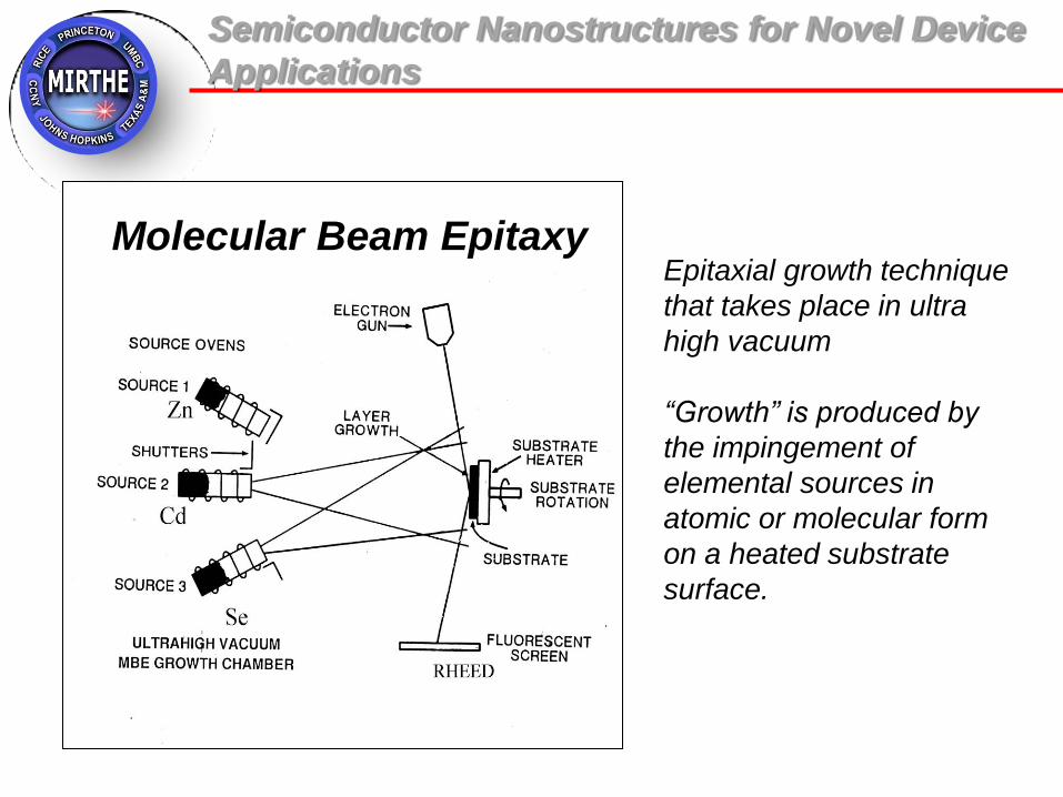
Epitaxial growth technique
that takes place in ultra
high vacuum
“Growth” is produced by
the impingement of
elemental sources in
atomic or molecular form
on a heated substrate
surface.
Molecular Beam Epitaxy
Semiconductor Nanostructures for Novel Device
Applications

Processes during Molecular Beam Epitaxy
9
Many different
processes compete at
the surface during
growth.
The growth conditions
determine which of
these dominate.
Ts, fluxes, substrate
surface orientation, etc.
Semiconductor Nanostructures for Novel Device
Applications

Frank-van der Merwe Volmer-Weber
monolayer-by-monolayer island growth
Layer-by-layer mode is
preferred for high
quality ultrathin layers:
Quantum Wells
MBE Growth Modes
Semiconductor Nanostructures for Novel Device
Applications
Near lattice-matched heteroepitaxy

11
type-I band alignment type-II band alignment
Semiconductor 2
Semiconductor 1
Semiconductor 1
Band Alignment
conduction
band
valence
band
Semiconductor Nanostructures for Novel Device
Applications

Quantum Wells
CB e2
e1
ΔEv VB
Band to band
Band-to-band
transition wavelength
depends on the QW
thickness ‘d’
quantum size effects h1 h2
ΔEc
Semiconductor Nanostructures for Novel Device
Applications
Barrier Barrier QW
d
Eg barrier
Eg well
discrete energy
levels in the well

5.1 5.4 5.7 6.0 6.3 6.6-1
0
1
2
3
4
5
6
7
8
3.0 3.3 3.6-1
0
1
2
3
4
5
6
7
8
BeSe
MgTe
HgTe
InSbInAs
GeGaSbSi
InPAlSb
GaAs
CdTeCdSeAlAsGaP
ZnTeAlPZnSe
ZnS MgSe
MgS
MgO
ZnO
AlN
GaN
Lattice Constant (A)
InN
Ban
dg
ap
en
erg
y a
t R
T (
eV
)Bandgap versus Lattice-Constant for Common Semiconductors
ZnCdMgSe/InP
Semiconductor Nanostructures for Novel Device
Applications

14
- 4 - 2 0 2 41 .5
2 .0
2 .5
3 .0
3 .5
4 .0
1 .5
2 .0
2 .5
3 .0
3 .5
4 .0
Z n T e
C d S e
Z n S e
M g S e
Ba
nd
ga
p E
ne
rg
y (
eV
)
L a t t ic e M is m a tc h to I n P ( % )
0 2 0 4 0 6 0 8 0 1 0 0
2 .0
2 .2
2 .4
2 .6
2 .8
3 .0 Z n
0 .5C d
0 .5S e
Z n0 .3
C d0 .4
M g0 .3
S e
Z n0 .3
C d0 .7
S e ( s t r a i n e d )
T = 1 0 K
En
erg
y (
eV
)
W e l l T h i c k n e s s ( Å )
ZnxCdyMg1-x-ySe on InP substrates
Semiconductor Nanostructures for Novel Device
Applications
• Bandgaps ranging from
2.1 – 3.2 eV (3.6 eV)
• Low defect densities
• n and p-type doping
• p+ contact layer
(ZnSeTe)

ZnxCd(1-x)Se/ZnxCdyMg(1-x-y)Se QWs on InP
0 20 40 60 80 100
2.0
2.2
2.4
2.6
2.8
3.0 Zn
0.5Cd
0.5Se
Zn0.3
Cd0.4
Mg0.3
Se
Zn0.3
Cd0.7
Se (strained)
T = 10K
Ene
rgy
(eV
)
Well Thickness ( Å)
Photoluminescence emission energy
as a function of QW thickness
InP substrate
InGaAs buffer
ZnCdMgSe
ZnCdMgSe ZnCdSe
QW
ZnCdSe
buffer
cap
Semiconductor Nanostructures for Novel Device
Applications
Appl. Phys Letters, 66, 2742 (1995)
App. Phys. Letters, 68, 3446 (1996)
QW structure

400 500 600 700
RT
521 nm
FWHM=17 nm551 nm
FWHM=18 nm
628 nm
FWHM=27 nm500 nm
FWHM=19 nm
Inte
nsity
(a.u
.)
Wavelength (nm)
-6 -4 -2 0 2 4 6
0
20
40
60
80
100
InP substrate
III-V buffer
ZnCdSe buffer
ZnxCdyMg1-x-ySe
ZnSeTe contact
ZnCdSe QW
n+
n
p
p+
nn
ZnxCdyMg1-x-ySe
Cur
rent
(mA
)
Voltage (V)
Light Emitting Diodes (LEDs)
RT Electroluminescence
ZnCdMgSe-based R-G-B Light Emitters
I-V Characteristics
Semiconductor Nanostructures for Novel Device
Applications
J. Crystal Growth 214/215, 1058 (2000)

Photopumped R-G-B laser diodes
604
nm
540
nm
497
nm
400 450 500 550 600 650
Pum
p
Inte
nsit
y (a
.u.)
Wavelength (nm)
Room temperature lasing spectra
for three DH laser structures
InP substrate
InGaAs buffer
ZnCdMgSe ZnCdSe
buffer
ZnCdMgSe
ZnCdSe
QW
cap
ZnCdMgSe
ZnCdMgSe
cladding
cladding
waveguide
waveguide
Double heterostructure (DH)
laser structure
Semiconductor Nanostructures for Novel Device
Applications
Appl. Phys. Lett., 70, 1351, (1997)
Appl. Phys. Lett., 72, 3136 (1998)
Exploring new Vertical External Cavity
Surface Emitting Laser (VECSEL)

Intersubband transitions
CB e2
e1
h1 h2
ΔEv VB
Barrier Barrier QW
Band to band
Intersubband CBO (ΔEc)
ISB transition
short
wavelength
limit is given by
the CBO
Need new materials with large CBO for shorter wavelength
Semiconductor Nanostructures for Novel Device
Applications
Intersubband
transition energy
depend ONLY on the
QW thickness ‘d’

Conduction band offset (CBO)
ZnMgSe (3.6eV, 0.1 µm)
50 Å ZnCdSe QW
ZnMgSe (3.6eV, 0.5 µm)
InP-SI substrate
InGaAs layer (0.1 µm)
ZnCdSe cap layer
LT-ZnCdSe buffer
∆Eg (Eg barrier – Eg well) = 1.5 eV
CBO = 0.8 ∆Eg ~1.12 eV
- 4 - 2 0 2 41 .5
2 .0
2 .5
3 .0
3 .5
4 .0
1 .5
2 .0
2 .5
3 .0
3 .5
4 .0
Z n T e
C d S e
Z n S e
M g S e
Ba
nd
ga
p E
ne
rg
y (
eV
)
L a t t ic e M is m a tc h to I n P ( % )
0 2 0 4 0 6 0 8 0 1 0 0
2 .0
2 .2
2 .4
2 .6
2 .8
3 .0 Z n
0 .5C d
0 .5S e
Z n0 .3
C d0 .4
M g0 .3
S e
Z n0 .3
C d0 .7
S e ( s t r a i n e d )
T = 1 0 K
En
erg
y (
eV
)
W e l l T h i c k n e s s ( Å )
o
ZnxCdyMg(1-x-y)Se
Appl. Phys. Lett. 83, 1995 (2003)
Semiconductor Nanostructures for Novel Device
Applications
Measured the CBO using
Contactless electroreflectance

Growth of doped MQW samples for FT-IR
Zn0.20Cd0.19Mg0.61Se, 0.1m
10X MQW
Zn0.20Cd0.19Mg0.61Se, 0.5m
SI-InP substrate
Zn0.20Cd0.19Mg0.61Se, 14nm
Zn0.5Cd0.5Se (n~1x10¹⁸) 5nm
Eg (barrier) = 3.0 eV
Eg (well) = 2.1 eV
CBO = 0.7 eV
- 4 - 2 0 2 41 .5
2 .0
2 .5
3 .0
3 .5
4 .0
1 .5
2 .0
2 .5
3 .0
3 .5
4 .0
Z n T e
C d S e
Z n S e
M g S e
Ba
nd
ga
p E
ne
rg
y (
eV
)
L a t t ic e M is m a tc h to I n P ( % )
0 2 0 4 0 6 0 8 0 1 0 0
2 .0
2 .2
2 .4
2 .6
2 .8
3 .0 Z n
0 .5C d
0 .5S e
Z n0 .3
C d0 .4
M g0 .3
S e
Z n0 .3
C d0 .7
S e ( s t r a i n e d )
T = 1 0 K
En
erg
y (
eV
)
W e l l T h i c k n e s s ( Å )
Zn0.5Cd0.5Se (n~1x10¹⁸) 5nm
Zn0.5Cd0.5Se (n~1x10¹⁸) 5nm
Semiconductor Nanostructures for Novel Device
Applications
ZnxCdyMg(1-x-y)Se

21
0.1 0.2 0.3 0.4 0.5 0.6
12 9 6 4 3
No
rma
lize
d A
bs
orb
an
ce
Energy (eV)
Sample A
Sample B
Sample C
RT
Wavelength (m)
15 20 25 30 35 40 45 50
3
4
5
6
7C
B
Ab
so
rpti
on
(m)
QW width (A)
Qc=0.70
Qc=0.75
Qc=0.80
Exp.
A
RT
ISB absorption in 4-7 m mid-IR
Bound-to-bound
Appl. Phys. Lett. 89, 131903 (2006)
A = 50Å, B = 40 Å, C = 30 Å
ISB absorption in MQWs: FT-IR spectroscopy
Semiconductor Nanostructures for Novel Device
Applications
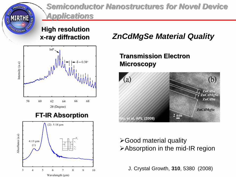
High resolution
x-ray diffraction
Wu, et al, APL (2009) FT-IR Absorption
Transmission Electron
Microscopy
Good material quality
Absorption in the mid-IR region
J. Crystal Growth, 310, 5380 (2008)
ZnCdMgSe Material Quality
Semiconductor Nanostructures for Novel Device
Applications

3-well active region graded “digital alloy” injector region 40 repeats of active/injector Waveguide layers for optical confinement
I
I
E=130 kV/cm
(>800 layers)
InP substrate:n–
InGaAs:n+
ZnCdSe n
ZnCdSe contact:n+
Active core
X 30
Injector (n doped)
Injector (n doped)
ZnCdSe n
ZnCdMgSe n
ZnCdMgSe n
Active region
ZnCdSe (LT)
waveguide
waveguide
Conduction band profile of active/injector region
QC Laser Structures
Semiconductor Nanostructures for Novel Device
Applications
Active
region

QC laser electroluminescence
Narrow EL FWHM (270 cm-1 to 220 cm-1)
Room temperature EL
App. Phys. Lett. 99, 041113 (2011) J. Electron. Mat. 41, 944 (2012)
• Fabricated QC emitters with Pt/Au metal contacts
Semiconductor Nanostructures for Novel Device
Applications

Dimensionality
QUANTUM
DOT
Semiconductor Nanostructures for Novel Device
Applications
d3
2-D structures:
quantum wells
d2
a
1-D structures:
quantum wires
a
b
0-D structures
a
b
c
lower dimensional structures exhibit more efficient
radiative recombination (i.e., light emission)

Frank-van der Merwe Volmer-Weber Stransky-Kranstanov
monolayer-by-monolayer island growth
MBE Growth Modes
self-assembled QDs
Strain-driven QD formation
Wetting
layer
Semiconductor Nanostructures for Novel Device
Applications

27
- 4 - 2 0 2 41 .5
2 .0
2 .5
3 .0
3 .5
4 .0
1 .5
2 .0
2 .5
3 .0
3 .5
4 .0
Z n T e
C d S e
Z n S e
M g S e
Ba
nd
ga
p E
ne
rg
y (
eV
)
L a t t ic e M is m a tc h to I n P ( % )
0 2 0 4 0 6 0 8 0 1 0 0
2 .0
2 .2
2 .4
2 .6
2 .8
3 .0 Z n
0 .5C d
0 .5S e
Z n0 .3
C d0 .4
M g0 .3
S e
Z n0 .3
C d0 .7
S e ( s t r a i n e d )
T = 1 0 K
En
erg
y (
eV
)
W e l l T h i c k n e s s ( Å )
ZnxCdyMg1-x-ySe on InP substrates
Semiconductor Nanostructures for Novel Device
Applications
• Bandgaps ranging from
2.1 – 3.2 eV (3.6 eV)
• Low defect densities
• n and p-type doping
• p+ contact layer
(ZnSeTe)

CdSe SAQDs on ZnCdMgSe
CdSe tD =10” (2 ML)
Height: 1.6 nm
Density: 1.02x109 cm-2
Radius: 30 nm
Ec
Ev
ZnCdMgSe CdSe
Type-I band alignment
Stranski-Krastanov Growth
Semiconductor Nanostructures for Novel Device
Applications
J. Cryst. Growth 294, 296–303 (2006)
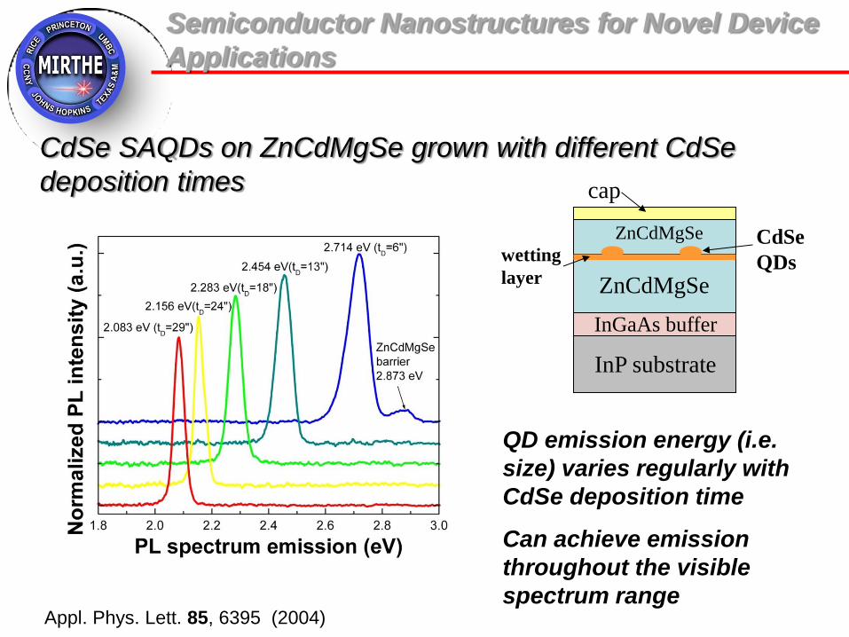
QD emission energy (i.e.
size) varies regularly with
CdSe deposition time
Can achieve emission
throughout the visible
spectrum range
CdSe SAQDs on ZnCdMgSe grown with different CdSe
deposition times
Semiconductor Nanostructures for Novel Device
Applications
InP substrate
InGaAs buffer
ZnCdMgSe
ZnCdMgSe
cap
CdSe
QDs wetting
layer
Appl. Phys. Lett. 85, 6395 (2004)

Stacked-QD LED structure
(white-light source)
Curr
ent
(A)
Voltage (V)
Room
temperature
PL emission
I-V
Semiconductor Nanostructures for Novel Device
Applications
J. Vac. and Sci. Technol. B 23, 1236 (2005)

Stacked multi-QD structures
ZnCdSe (70 Å)
ZnCdSe (60 Å)
ZnCdMgSe (1300 Å)
InP (SI)
ZnCdMgSe
InGaAs (1500 Å)
ZnCdSe
ZnCdMgSe ZnCdMgSe
spacer
CdSe QDs (tD=10”) 29x
Stacked or multi-QD
structure
5 µm
2.5 µm
0 µm
5 µm
2.5 µm
0 µm
7.77 nm
3.89 nm
0 nm
5 µm
2.5 µm
0 µm 0 µm
2.5 µm
5 µm
7.77 nm
AFM image of an uncapped
multi-QD structure:
Lateral alignment: quantum
wires?
Semiconductor Nanostructures for Novel Device
Applications
J. Vac. Sci. Technol. B 24, 1649 (2006)
Stacked QD layers are
vertically aligned

32
type-I band alignment type-II band alignment
Semiconductor 2
Semiconductor 1
Semiconductor 1
Band Alignment
conduction
band
valence
band
Semiconductor Nanostructures for Novel Device
Applications

GaAs Substrate
ZnSe Spacer
ZnSe Spacer
ZnSe Spacer
ZnSe
Zn
Te
Zn
Te
Zn
Te
Zn
ZnSe Buffer
× Nperiods
ZnSe Spacer
Shutter sequence
< 1ML ZnTe:N
Submonolayer type-II QDs
Semiconductor Nanostructures for Novel Device
Applications
Migration Enhanced Epitaxy

< 1ML ZnTe:N
Shutter sequence
Zn
Te
Zn
Te
Zn
Te
Zn
GaAs Substrate
ZnSe Spacer
ZnSe Spacer
ZnSe Spacer
ZnSe
ZnSe Buffer
× Nperiods
ZnSe Spacer
New composite
material made
up of ZnTe
nanoislands
embedded in a
matrix of ZnSe
Submonolayer type-II QDs
Semiconductor Nanostructures for Novel Device
Applications
Phys. Rev. B 77, 15534 (2008)
Migration Enhanced Epitaxy

Frank-van der Merwe Volmer-Weber Stransky-Kranstanov
monolayer-by-monolayer
MBE Growth Modes
self-assembled QDs
Wetting
layer
Semiconductor Nanostructures for Novel Device
Applications
island growth
No wetting layer

Evidence for type-II alignment:
Energy shift of the “green band”
“blue band” “green band”
Ec
Ev
Type I
+
_ A B
Ec
Ev
Type II
+
_
Semiconductor Nanostructures for Novel Device
Applications
Spatial separation of carriers

“blue band” “green band” weak excitation strong excitation
hweak < hstrong
Semiconductor Nanostructures for Novel Device
Applications
Evidence for type-II alignment:
Energy shift of the “green band”

“blue band” “green band”
Figure 2.2: The probability densities of the
ground electron and hole states in type-II
ZnTe/ZnSe QDs.
Spatial separation of electrons and holes and other interesting phenomena
May result in enhanced materials properties for Photovoltaics
Semiconductor Nanostructures for Novel Device
Applications
Phys. Rev. B. 71, 045340 (2005)
Evidence for type-II alignment:
Energy shift of the “green band”

Evidence for QDs:
Structural characterization & magneto optics
TEM studies indicate the presence of stacked nanoislands of high Te content
Magneto optical studies show characteristic signature of 0-d structures (Aharonov-Bohm Effect)
TEM Characterization
J. Appl. Phys. 99, 064913 (2006)
Semiconductor Nanostructures for Novel Device
Applications

Intermediate band solar cell (IBSC)
• An IBSC has an intermediate band (IB)
material with a band of states within the band
gap of the host semiconductor.1,2
• Absorption of below band gap photons is
possible without significant reduction in open
circuit voltage.
• An optimal IBSC with an efficiency of about
63%, has a host band gap of 1.95 eV, and an
IB at 0.71 eV. 1,2
• Can be fabricated using semiconductor QDs
embedded in a host semiconductor matrix.
• Challenges: Unavailability of the appropriate
material systems.3
1Luque, A. & Martí, Phys. Rev. Lett. 78, 5014-5017 (1997). 2Luque, A., Martí, A. & Stanley, C. Nature Photon. 6, 146-152 (2012). 3Luque, A. & Martí, A. Adv. Mater. 22, 160-174 (2010).
Semiconductor Nanostructures for Novel Device
Applications

- 4 - 2 0 2 41 .5
2 .0
2 .5
3 .0
3 .5
4 .0
1 .5
2 .0
2 .5
3 .0
3 .5
4 .0
Z n T e
C d S e
Z n S e
M g S e
Ba
nd
ga
p E
ne
rgy
( e
V )
L a t t ic e M is m a tc h to I n P ( % )
0 2 0 4 0 6 0 8 0 1 0 0
2 .0
2 .2
2 .4
2 .6
2 .8
3 .0 Z n
0 .5C d
0 .5S e
Z n0 .3
C d0 .4
M g0 .3
S e
Z n0 .3
C d0 .7
S e ( s t r a i n e d )
T = 1 0 K
En
erg
y (
eV
)
W e l l T h i c k n e s s ( Å )
o
ZnxCdyMg(1-x-y)Se
ZnCdSe
Eg ~2.1 eV
Semiconductor Nanostructures for Novel Device
Applications
ZnTe
QDs
Proposed (ideal) material for IBSCs

ZnTe QDs in ZnCdSe
• ZnCdSe has a band gap of ~ 2.1 eV
when lattice matched to InP.
• ZnTe-ZnCdSe valence band offset is
0.8 – 1.0 eV.
• Intermediate band at ~ 0.7 eV can
be engineered from the hole
confinement energy level within
ZnTe QDs.
• Type-II band alignment is expected
to suppress both radiative and Auger
recombination and improve the
carrier extraction process
significantly.
Parameters for an ideal IBSC:
Host semiconductor band gap ≈ 1.95 eV
IB at ≈ 0.71 eV
Semiconductor Nanostructures for Novel Device
Applications

• Samples were grown by combination of molecular
beam epitaxy (MBE) and migration enhanced
epitaxy (MEE)
• During MEE, only submonolayer quantities of Zn,
and Te were used along with a specific shutter
sequence.
• .
ZnTe type-II QDs in ZnCdSe
InP Substrate
ZnCdSe Spacer
ZnCdSe Spacer
ZnCdSe
ZnCdSe Buffer
× Nperiods
ZnCdSe Spacer
ZnCdSe Spacer
Expected structure
Semiconductor Nanostructures for Novel Device
Applications
J. Vac. Sci. Technol. B 31(3) C119 (2013).

Optical properties: type-II band alignment
• The HRXRD confirms the high structural quality of the sample
• The excitation intensity dependent PL at 10K showed a shift in PL energy,
demonstrating the type-II nature of the multilayered structure.
Blue
band Green
band
Semiconductor Nanostructures for Novel Device
Applications
HRXRD Photoluminescence (PL)

Vertical correlation and miniband formation
ensure sufficient overlap of the QD confined hole wave functions to facilitate the
miniband formation.
Formation of miniband needed for successful operation of an IBSC to increase
below band gap absorption
Semiconductor Nanostructures for Novel Device
Applications
Exploring growth of larger QDs to achieve vertical correlation

46
• Band structure engineering of semiconductor materials gives rise to a
myriad of novel physical phenomena and device functionalities
• Alloying, heterojunctions, low dimensionality, strain phenomena and
band alignment are some of the parameters that can be manipulated
for bandstructure engineering and device design
• R-G-B light emitters based on band-to-band emission in QW-based
structures of ZnCdMgSe have been demonstrated
• Devices based on intersubband transitions, such as QC lasers and
detectors, and QW infrared photodetetctors (QWIPs) are being
pursued for shorter wavelength applications in the mid-IR
• Strain effects are exploited to fabricate self-assembled QDs in
ZnCdMgSe structures that have shown potential for light emitting
devices
• Type-II QDs and the resultant spatial separation of carriers are being
explored for photovoltaic applications in IBSC
Semiconductor Nanostructures for Novel Device
Applications
Summary
47
Semiconductor Nanostructures for Novel Device
Applications
Acknowledgements: Linfei Zeng, Ning Dai, Abdullah Cavus, Wilson Lin, Catherine
Luo, Oleg Maksimov, Mohammad Sohel, Zuecong Zhou, Noemi
Perez-Paz, Hong Lu, Martin Muñoz, Shiping Guo, William
Charles, Kale Franz, Adrian Alfaro-Martinez, Yu Yao, Qiang
Zhang, Richard Moug, Joel de Jesus, Thor Axtmann Garcia,
Vasilios Deligiannakis, Arvind Ravikumar, Siddarth Dhombar
Aidong Shen, Igor Kuskovsky, I. Cevdet Noyan, Claire Gmachl


![SPIN CURRENTS IN SEMICONDUCTOR NANOSTRUCTURES: A ...bnikolic/PDF/spin_currents_oup.pdf · arXiv:0907.4122v1 [cond-mat.mes-hall] 23 Jul 2009 SPIN CURRENTS IN SEMICONDUCTOR NANOSTRUCTURES:](https://img.dokumen.tips/doc/110x75/5f336dbb72f2ec2b812bb7bc/spin-currents-in-semiconductor-nanostructures-a-bnikolicpdfspincurrentsouppdf.jpg)