Embed Size (px)
Citation preview

© 2016 WILEY-VCH Verlag GmbH & Co. KGaA, Weinheim2896 wileyonlinelibrary.com
CO
MM
UN
ICATI
ON Self-Powered High-Resolution and Pressure-Sensitive
Triboelectric Sensor Matrix for Real-Time Tactile Mapping
Xiandi Wang , Hanlu Zhang , Lin Dong ,* Xun Han , Weiming Du , Junyi Zhai , Caofeng Pan , * and Zhong Lin Wang
X. Wang, H. Zhang, Prof. L. Dong, X. Han, W. Du, Prof. J. Zhai, Prof. C. F. Pan, Prof. Z. L. Wang Beijing Institute of Nanoenergy and Nanosystems Chinese Academy of Sciences 30 Xueyuan Road , Beijing 100083 , P. R. China E-mail: [email protected]; [email protected] Prof. Z. L. Wang School of Materials Science and Engineering Georgia Institute of Technology Atlanta , GA 30332–0245 , USA
DOI: 10.1002/adma.201503407
Here, we report a self-powered, high-resolution, and pres-sure-sensitive TESM based on single-electrode triboelectric generators that enable real-time tactile mapping. When an object moves on the top surface of a polydimethylsiloxane (PDMS) layer, the corresponding electrical response of the TESM is obtained from the charge transfer between the elec-trodes and the ground on the basis of the coupling effect between contact electrifi cation and electrostatic induction. A fl exible 16 × 16 pixelated TESM with a resolution of 5 dpi can map single-point and multi-point tactile stimuli in real time via the multichannel data acquisition method while maintaining an excellent pressure sensitivity of 0.06 kPa −1 and long-term durability. To simplify the device structure and enhance the addressing speed for larger matrices, a cross-type TESM with 36 × 20 pixels was demonstrated; this cross-type TESM can sig-nifi cantly reduce the number of addressing lines from m × n to m + n , which greatly shortens the measurement period and is benefi cial for real-time tactile mapping. The triboelectric sensor matrix exhibits distinct merits, including lower costs and the ability to self-power, in comparison to traditional motion sen-sors, indicating that this device has widespread potential in tac-tile sensing for touchpad, robotics, and human-machine inter-face applications.
Figure 1 a shows a schematic of the self-powered fl exible single-electrode triboelectric sensor matrix. A square piece of polyethylene glycol terephthalate (PET) fi lm with a thickness of 250 µm was utilized as the fl exible dielectric substrate; this fi lm was overlapped by predesigned masks with different patterns on both sides, and then arrayed through-holes were drilled by laser cutting. Next, a layer of Ag was deposited by magnetron sputtering onto both sides of the substrate; these layers serve as patterned Ag electrodes after the mask was peeled away. The electrodes consist of two parts: The aligned regular electrode array on the top side that serves as the charge-sensing element and the circuit confi guration electrodes on the bottom side that connect to external measuring equipment; the electrode array and the confi guration electrodes interconnect with each other via the through-holes (Figure S1, Supporting Information). To ensure a perfect electrical connection, the sputtering time was extended to increase the thickness of the Ag layer. Then, another thin fi lm of PET with ethylene–vinyl acetate copolymer (EVA) was used to cover the bottom side to encapsulate the cir-cuit confi guration electrodes. A PDMS fi lm was spin-coated onto the top and subsequently cured; this fi lm serves as the electrifi cation layer that generates triboelectric charges when being touched. To enhance the triboelectric effect, the cured PDMS layer was dry etched to produce a micro/nanostructured surface to increase the effective charge density, as shown in Figure 1 b. Actually, other materials, including polyvinyl alcohol,
Flexible tactile sensors are essential components in the elec-tronic skin, which is designed to mimic the comprehensive properties of human sensing via electronics. [ 1 ] The achievement of a high-performance tactile sensor is a highly interesting topic for a wide range of applications in artifi cial intelligence, prosthetics, health monitoring, and human-machine inter-actions. [ 2 ] Signifi cant breakthroughs have been achieved in high-sensitivity, high-resolution, and large-scale pressure sen-sors based on different physical transduction mechanisms, including piezoresistivity, [ 3 ] capacitance, [ 4 ] and piezoelectricity. [ 5 ] Recently, many research groups have started to develop multi-functional tactile sensors that are self-healing, [ 6 ] self-powered, [ 7 ] and transmit wirelessly. [ 8 ] However, little research has been reported on high-resolution and high-sensitive tactile sensors with low power consumption for real-time trajectory mapping.
Large-scale and pressure-sensitive sensor matrices based on transistor switches have been developed because the one-way current-passing characteristic of the transistor can enormously reduce both crosstalk among pixels and power consumption. [ 9 ] However, the output signal, which is always based on the resis-tance or capacitance, rapidly changes when the external pressure disappears, which makes continuous monitoring and imaging using serial data readings diffi cult. In contrast, we previously developed an all-optical high-resolution pressure sensor matrix to collect images in real-time of the 2D strain distribution in parallel on the basis of the piezophototronic or piezophotonic effect, with low pressure sensitivity. [ 10 ] Fortunately, the triboelectric generator/sensors were fi rst demonstrated by Wang and co-workers. [ 11 ] These sensors convert random mechanical energy into elec-trical signals without power consumption [ 12 ] but also exhibit out-standing pressure sensitivity. [ 13 ] Additionally, triboelectric charges remain on the surface of insulators until opposite charges are induced to regain the electrostatic equilibrium, which is condu-cive to real-time tactile mapping. [ 14 ] In recent years, different tribo-electric sensor matrices (TESMs) have been developed, including dual-electrode-based [ 15 ] and single-electrode-based matrices, [ 16 ] all of which are small-scale and have a low resolution.
Adv. Mater. 2016, 28, 2896–2903
www.advmat.dewww.MaterialsViews.com

2897wileyonlinelibrary.com© 2016 WILEY-VCH Verlag GmbH & Co. KGaA, Weinheim
CO
MM
UN
ICATIO
N
polytetrafl uoroethylene, and fl uorinated ethylene propylene, can be utilized as the electrifi cation layer material. A photo-graph of an as-fabricated self-powered fl exible 16 × 16 pixelated
TESM with a resolution of 5 dpi is shown in Figure 1 c, and the side length of each pixel is 2.5 mm. In addition, the pixel size can be reduced to the micron-size level using a microfabrication technology for more precise tactile sensing. A square pixel with 500 µm side length was used as the smallest pixel size in our experiment.
The working principle of the TESM is based on the single-electrode triboelectric nanogenerator, which can be explained by the coupling effect between contact electri-fi cation and electrostatic induction (details can be found in Figure S2 in the Sup-porting Information). [ 17 ] The typical electrical responses of the single-electrode triboelectric sensor under an external contact process are shown in Figure S3 in the Supporting Infor-mation, where the contact area between the Al foil and the PDMS fi lm is 16 cm 2 . The device structure and the schematic of the measuring circuit are shown in the inset of
Figure 2 a. Notably, the measured open-circuit voltage, which represents the electric potential difference between two ends of the external resistor in our experiments, changed from a
Adv. Mater. 2016, 28, 2896–2903
www.advmat.dewww.MaterialsViews.com
Figure 1. Structure of the TESM. a) Schematic of a 16 × 16 TESM. Insets: Partially enlarged tilted view and cross-sectional view of the structural design of the top and bottom, respectively. b) Scanning electron microscopy (SEM) image of the etched PDMS surface microstructure. c) Photograph of a fabricated 16 × 16 TESM with good fl exibility.
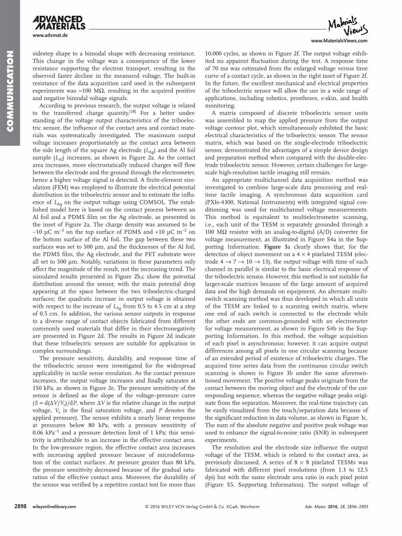
Figure 2. Electrical output characteristics of a triboelectric sensor. a) The output voltage increases with increasing contact area at a pressure of ≈200 kPa. The size ratio between the Ag electrode and Al foil was maintained at 1. b) The output voltage simulated using the fi nite element method with different contact areas. Insets: Sectional views of the simulated potential distribution for the sensor with side lengths of 0.5 and 4.5 cm. c) FEM simulation of the potential distribution around the sensor with a side length of 4.5 cm when the Al foil is kept at a distance of 0.5 mm. d) The output voltage of the sensor with a square Ag electrode (1 cm side length) in response to different contact materials (1 cm side length) at a pressure of ≈200 kPa. e) The output voltage as a function of pressure. The triboelectric sensor exhibits excellent pressure sensitivity in the range from 1 to 80 kPa. f) The durability and time response tests for pressure sensing with an Ag electrode (1 cm side length) with a continuous loading/unloading of a periodic force in contact with an Al foil (1 cm side length). Insets: Partially enlarged views of the voltage versus time curve.
2898 wileyonlinelibrary.com © 2016 WILEY-VCH Verlag GmbH & Co. KGaA, Weinheim
CO
MM
UN
ICATI
ON sidestep shape to a bimodal shape with decreasing resistance.
This change in the voltage was a consequence of the lower resistance supporting the electron transport, resulting in the observed faster decline in the measured voltage. The built-in resistance of the data acquisition card used in the subsequent experiments was ≈100 MΩ, resulting in the acquired positive and negative bimodal voltage signals.
According to previous research, the output voltage is related to the transferred charge quantity. [ 18 ] For a better under-standing of the voltage output characteristics of the triboelec-tric sensor, the infl uence of the contact area and contact mate-rials was systematically investigated. The maximum output voltage increases proportionately as the contact area between the side length of the square Ag electrode ( L Ag ) and the Al foil sample ( L Al ) increases, as shown in Figure 2 a. As the contact area increases, more electrostatically induced charges will fl ow between the electrode and the ground through the electrometer, hence a higher voltage signal is detected. A fi nite-element sim-ulation (FEM) was employed to illustrate the electrical potential distribution in the triboelectric sensor and to estimate the infl u-ence of L Ag on the output voltage using COMSOL. The estab-lished model here is based on the contact process between an Al foil and a PDMS fi lm on the Ag electrode, as presented in the inset of Figure 2 a. The charge density was assumed to be −10 µC m −2 on the top surface of PDMS and +10 µC m −2 on the bottom surface of the Al foil. The gap between these two surfaces was set to 500 µm, and the thicknesses of the Al foil, the PDMS fi lm, the Ag electrode, and the PET substrate were all set to 500 µm. Notably, variations in these parameters only affect the magnitude of the result, not the increasing trend. The simulated results presented in Figure 2 b,c show the potential distribution around the sensor, with the main potential drop appearing at the space between the two triboelectric-charged surfaces; the quadratic increase in output voltage is obtained with respect to the increase of L Ag from 0.5 to 4.5 cm at a step of 0.5 cm. In addition, the various sensor outputs in response to a diverse range of contact objects fabricated from different commonly used materials that differ in their electronegativity are presented in Figure 2 d. The results in Figure 2 d indicate that these triboelectric sensors are suitable for application in complex surroundings.
The pressure sensitivity, durability, and response time of the triboelectric sensor were investigated for the widespread applicability in tactile sense emulation. As the contact pressure increases, the output voltage increases and fi nally saturates at 150 kPa, as shown in Figure 2 e. The pressure sensitivity of the sensor is defi ned as the slope of the voltage–pressure curve ( S = d(Δ V / V s )/d P , where Δ V is the relative change in the output voltage, V s is the fi nal saturation voltage, and P denotes the applied pressure). The sensor exhibits a nearly linear response at pressures below 80 kPa, with a pressure sensitivity of 0.06 kPa −1 and a pressure detection limit of 1 kPa; this sensi-tivity is attributable to an increase in the effective contact area. In the low-pressure region, the effective contact area increases with increasing applied pressure because of microdeforma-tion of the contact surfaces. At pressure greater than 80 kPa, the pressure sensitivity decreased because of the gradual satu-ration of the effective contact area. Moreover, the durability of the sensor was verifi ed by a repetitive contact test for more than
10,000 cycles, as shown in Figure 2 f. The output voltage exhib-ited no apparent fl uctuation during the test. A response time of 70 ms was estimated from the enlarged voltage versus time curve of a contact cycle, as shown in the right inset of Figure 2 f. In the future, the excellent mechanical and electrical properties of the triboelectric sensor will allow the use in a wide range of applications, including robotics, prostheses, e-skin, and health monitoring.
A matrix composed of discrete triboelectric sensor units was assembled to map the applied pressure from the output voltage contour plot, which simultaneously exhibited the basic electrical characteristics of the triboelectric sensor. The sensor matrix, which was based on the single-electrode triboelectric sensor, demonstrated the advantages of a simple device design and preparation method when compared with the double-elec-trode triboelectric sensor. However, certain challenges for large-scale high-resolution tactile imaging still remain.
An appropriate multichannel data acquisition method was investigated to combine large-scale data processing and real-time tactile imaging. A synchronous data acquisition card (PXIe-4300, National Instruments) with integrated signal con-ditioning was used for multichannel voltage measurements. This method is equivalent to multielectrometer scanning, i.e., each unit of the TESM is separately grounded through a 100 MΩ resistor with an analog-to-digital (A/D) converter for voltage measurement, as illustrated in Figure S4a in the Sup-porting Information. Figure 3 a clearly shows that, for the detection of object movement on a 4 × 4 pixelated TESM (elec-trode 4 → 7 → 10 → 13), the output voltage with time of each channel in parallel is similar to the basic electrical response of the triboelectric sensor. However, this method is not suitable for larger-scale matrices because of the large amount of acquired data and the high demands on equipment. An alternate multi-switch scanning method was thus developed in which all units of the TESM are linked to a scanning switch matrix, where one end of each switch is connected to the electrode while the other ends are common-grounded with an electrometer for voltage measurement, as shown in Figure S4b in the Sup-porting Information. In this method, the voltage acquisition of each pixel is asynchronous; however, it can acquire output differences among all pixels in one circular scanning because of an extended period of existence of triboelectric charges. The acquired time series data from the continuous circular switch scanning is shown in Figure 3 b under the same aforemen-tioned movement. The positive voltage peaks originate from the contact between the moving object and the electrode of the cor-responding sequence, whereas the negative voltage peaks origi-nate from the separation. Moreover, the real-time trajectory can be easily visualized from the touch/separation data because of the signifi cant reduction in data volume, as shown in Figure 3 c. The sum of the absolute negative and positive peak voltage was used to enhance the signal-to-noise ratio (SNR) in subsequent experiments.
The resolution and the electrode size infl uence the output voltage of the TESM, which is related to the contact area, as previously discussed. A series of 8 × 8 pixelated TESMs was fabricated with different pixel resolutions (from 1.3 to 12.5 dpi) but with the same electrode area ratio in each pixel point (Figure S5, Supporting Information). The output voltage of
Adv. Mater. 2016, 28, 2896–2903
www.advmat.dewww.MaterialsViews.com

2899wileyonlinelibrary.com© 2016 WILEY-VCH Verlag GmbH & Co. KGaA, Weinheim
CO
MM
UN
ICATIO
N
each pixel, which decreased as the resolution improved, was measured under the contact/separation of a rubber capacitive stylus. Another series was also investigated with a resolution of 5 dpi and an L Ag ranging from 0.5 to 4.5 mm (photographs given in Figure S6 in the Supporting Information). The statis-tical results show that the output voltage is directly proportional to the L Ag , as shown in Figure 3 d, indicating that the increase in the electrode’s area ratio in each pixel can improve the SNR of the sensor.
The large-scale TESM is capable of tracking the trajectory of an object moving on its surface. The speed of the moving object is also a key parameter that infl uences the performance of the trajectory imaging. First, a shorter measurement cycle period was adopted to ensure the accuracy of the trajectory tracking; whereas a longer period would result in missing data points when the objects move at a high speed. In our experiments, the switch interval was set to 2.5 ms, which is also advanta-geous for fast data processing and real-time imaging because of the relatively smaller data volume. Second, the change in effective contact area per unit time was dependent on the
object’s speed, resulting in a change in the output voltage. To gain a better understanding, we systematically investigated tac-tile imaging of an 8 × 8 pixelated TESM in contact mode and sliding mode. The test methods and homemade testing board are presented in Figure S7 in the Supporting Information. In contact mode, the speed of approach/separation and the touching-time interval do not signifi cantly infl uence the ampli-tude of the output when the contact area between the object and the electrode are kept constant, as shown in Figure S8 in the Supporting Information. However, in the sliding mode, the measured voltage increased as the sliding speed of the capacitive stylus over the TESM in a straight path increased. This endowed the corresponding trajectory map with a better SNR, as shown in Figure 4 a. Figure 4 b presents an enlarged view of the acquired signal when the stylus moved at a speed of 10 mm s −1 , where the voltage peaks corresponding to the pixel in each scanning cycle were determinately marked out. Three peaks were collected as the stylus slid across each pixel, which means the change in the effective contact area per cycle is approximately one-third the area of the electrode in each
Adv. Mater. 2016, 28, 2896–2903
www.advmat.dewww.MaterialsViews.com
Figure 3. Measurement method for tactile mapping and the infl uence of the electrode area ratio on the electrical properties. The voltage signals acquired using (a) the synchronous data acquisition card and (b) the multiswitch scanning method when a capacitive stylus touched the surface of a 4 × 4 TESM along a path: E4 → E7 → E10 → E13. Inset of (a): Illustration showing the moving direction of the stylus. c) Mapping fi gures showing the motion trail visualized by a computer program utilizing the negative voltage peaks, the positive voltage peaks, and the sum of the absolute values of the negative and positive voltage peaks, respectively. d) The dependence of the measured output voltage on the side length of the Ag electrode. Multiple pixels (the error bars with different colors) of each TESM were measured. The increase in the electrode’s area ratio in each pixel can enhance the output at a certain resolution.

2900 wileyonlinelibrary.com © 2016 WILEY-VCH Verlag GmbH & Co. KGaA, Weinheim
CO
MM
UN
ICATI
ON
pixel. According to the acquired output voltages, the trajec-tory tracking process was realized by utilizing positive voltage signals, negative voltage signals, and whole voltage signals, respectively (top to bottom), as presented in Figure 4 c and Figure S9 in the Supporting Information.
The ability to identify various touch modes, such as single-point touch, sliding, and multi-point touch, is one of the most important prerequisites for practical application in user-machine interactive operations. As previously discussed, the TESM can easily respond to single-point touch. Figure 5 a pre-sents a schematic of the electrodes of a 16 × 16 pixelated TESM and the order of the stylus in contact with different pixels, on which a “G” shape is marked. Figure 5 b shows the fi nal corre-sponding visualized touch trajectory map (Video S1, Supporting Information). As shown in Figure 5 c, the mapping quality could be further improved by utilizing a fi ltering program to fade out other crosstalk signals in the monitoring process. The TESM can also sense multi-point touch and image pressure distribution. FEM simulation about the single-point and multi-point touch sensing was performed using COMSOL. Figure 5 d presents the simulated result in uni-point, bi-point, and multi-point touch sensing; the potential distinction between the touched and untouched electrodes is intuitively observed, theoretically verifying the feasibility of sensing multi-point touch by the TESM. Figure 5 e is a schematic of how the the sensor matrix images the pressure distribution when a mold in the shape of a “6” is pressed against the top of the TESM. The experimental mapping result is given in Figure 5 f, from
which the shape of the mold could be readily imaged through the simultaneous use of multiple pixels.
When the scale of the sensor matrix is further enlarged, the circuit confi guration on the bottom side of the TESM becomes more complicated. Additionally, the larger number of addressing lines ( m × n ) will present further challenges to achieving fast mapping. To overcome these challenges, we developed a novel cross-type TESM that can reduce the number of scanning channels to just m + n and simplify the device struc-ture. A schematic of the electrode structure design is shown in Figure 6 a. An in-plane aligned rhombic array confi guration was adopted to increase the electrode’s area ratio in each pixel at a certain resolution. Electrodes in each row are electrically connected along the diagonal direction via connecting lines on the top surface of the PET substrate, while electrodes in each column are connected by the lines on the backside. A photo-graph of an 8 × 8 cross-type TESM with a pixel resolution of 5 dpi is shown in Figure 6 b.
The touch-locating method of this cross-type TESM is based on the cross-locating technology. Voltage signals can be mea-sured from both the corresponding row and column ports when an object touches the intersection. Figure 6 d presents the measured signal using the synchronous data acquisition card and shows the detailed locating process when a stylus touches the intersections of row 3 and column 3 (X3Y3, noted as A), row 7 and column 5 (X7Y5, noted as B), and row 5 and column 7 (X5Y7, noted as C) in turn (Video S2, Supporting Informa-tion). Additionally, real-time visualized tactile mapping was
Adv. Mater. 2016, 28, 2896–2903
www.advmat.dewww.MaterialsViews.com
Figure 4. Infl uence of the speed of moving objects on the performance of trajectory imaging. a) Measured output voltage signals of an 8 × 8 TESM and corresponding trajectory mapping at various stylus speeds (2, 5, 10, 20, and 50 mm s −1 ). b) Enlarged view of the measured signal when the stylus slides at a speed of 10 mm s −1 . Each voltage peak was marked corresponding to the pixel in each scanning cycle (distinguished by the dotted line). c) Illustration of the moving process and trajectory imaging. From top to bottom in each inset are the positive voltage signals, the negative voltage signals, and the whole voltage signals, which were used to map the object’s trajectory.

2901wileyonlinelibrary.com© 2016 WILEY-VCH Verlag GmbH & Co. KGaA, Weinheim
CO
MM
UN
ICATIO
N
Adv. Mater. 2016, 28, 2896–2903
www.advmat.dewww.MaterialsViews.com
Figure 6. Design and electrical characteristics of cross-type TESM for large-scale tactile imaging. a) Electrode structural design of the cross-type TESM. b) Photograph of an 8 × 8 cross-type TESM with a pixel resolution of 5 dpi. c) Voltage signals measured using a multiswitch scanning method when a capacitive stylus touches three specifi c nodes on the sensor. Inset: Tactile mapping acquired from the voltage signals. d) Voltage signal measured using the synchronous data acquisition card, and the schematics of the data processing method for tactile mapping by the cross-type TESM. e) Demonstra-tion of a 36 × 20 cross-type TESM fabricated with transparent ITO electrodes attached to a commercial cell phone in which a touching trail of a “3” by a fi nger is indicated. f) Diagrams of the processed voltage signals obtained and the fi nal tactile mapping.
Figure 5. Identifi cation of single-point touch and multi-point touch mode. a) Illustration of the single-point contact on a 16 × 16 TESM pixel in pixels along a specifi c path of “G”. b) Trajectory map obtained from the detected voltages when a capacitive stylus contacts the matrix along the route speci-fi ed in panel (a). c) A high-SNR trajectory map was obtained using a fi ltering program that can fi lter out other crosstalk signals in each scanning cycle. d) Schematic of the pressure mapping process. e) Demonstration of the mapping output voltage of the sensor matrix under the pressure of a module in the shape of a “6”. f) FEM simulation results for the potential distribution in uni-point, bi-point, and multi-point touch sensing.

2902 wileyonlinelibrary.com © 2016 WILEY-VCH Verlag GmbH & Co. KGaA, Weinheim
CO
MM
UN
ICATI
ON
Adv. Mater. 2016, 28, 2896–2903
www.advmat.dewww.MaterialsViews.com
obtained by using a multiswitch scanning method, as shown in Figure 6 c. Two voltage peaks were acquired in each scanning cycle, which correspond to the coordinates of the contact points.
The cross-type TESM with low-power consumption and rapid addressing is highly suitable for the construction of large-scale and fl exible e-skin for use in prostheses, robotics, and human-machine interfaces. A simple touch-panel application is demonstrated in Figure 6 e,f. A 36 × 20 TESM with a pixel reso-lution of 10 dpi was fabricated; the electrode material was sub-stituted by transparent indium tin oxide (ITO), which is widely used in commercial capacitive touch screens. Figure 6 f presents the tactile map obtained when a nitrile-gloved fi nger traced a “3” on the surface of the TESM. A striking contrast between the touched and untouched pixels was observed, revealing the practicability of the TESM in user-interactive interfaces for con-sumer electronics.
In summary, we developed a self-powered high-resolution and pressure-sensitive TESM for the visualization of touch actions or tracking motion trajectories in real-time. The output electric signals generated by the coupling effect between con-tact electrifi cation and electrostatic induction are related to the effective contact area between the monitored object and the surface of the TESM, and no external electrical power is needed. With the assistance of a customized data acquisition and processing system, a 16 × 16 pixelated TESM with high pressure sensitivity and long-term durability was demonstrated and applied to the real-time visualization of single-point touch trajectory and multi-point pressure distribution. Additionally, a cross-type TESM based on cross-locating technology was dem-onstrated; this TESM can further rapidly map touch actions. A 36 × 20 cross-type TESM with transparent ITO electrodes was fabricated to track the sliding trajectory of a nitrile-gloved fi nger as an alternative touch screen instead of the capacitive screen that is widely used in commercial cell phones. We anticipate that this device will open exciting opportunities for the broad application of real-time tactile mapping in motion tracking, touch sensing, and human-machine interfaces.
Experimental Section Fabrication of the TESM and Single Triboelectric Sensor : For the
fabrication of the TESM, a 250-µm-thick fl exible PET fi lm was covered with commercial Kapton tape on both sides. Laser cutting was then used to selectively erase the Kapton tape as predesigned to form a mask pattern on both sides; localized through-holes were subsequently drilled on the PET substrate. Ag or ITO was then deposited via magnetron sputtering (100 W, 20 min, ambient temperature, 3 mTorr) onto both sides of the substrate through the mask as electrodes. The mask was peeled away, and the side of the substrate with the designed circuit confi guration was encapsulated using a 100-µm-thick EVA-covered PET tape; a fi lm of uncured PDMS (Sylgard 184 silicone elastomer, mixed well at a 1:10 weight-ratio of curing agent:polymer) was then spun onto the other side with arrayed square electrodes. After the PDMS was cured at 75 °C for 4–6 h, a micro/nanostructure was constructed on the surface of the PDMS by reactive-ion etching using oxygen plasma for 1 h at a pressure of ≈180 mTorr. The morphology of the etched PDMS surface was characterized using fi eld-emission scanning electron microscopy (Hitachi SU8020). For a single triboelectric sensor, the fabrication process was similar, except that the electrode was deposited onto only one side, no through-holes were drilled, and the encapsulation was not necessary.
Preparation of the Contact Objects : To study the electrical characteristics of the triboelectric sensor, an acrylic sheet with a thickness of 5 mm was cut to the desired substrate dimensions. As the contact surface, a piece of Al foil or other material of the desired size was adhered onto the acrylic substrate using double-sided sticky tape. For the sliding motion detection and single-point touch, a commercial capacitive touch pen was used as the contact object. For the pressure imaging tests, 2-mm-thick synthetic rubber was cut into the desired shape and then adhered onto an acrylic support.
Measurement Setup : For the triboelectric sensors, the output voltage was measured using a high-impedance electrometer (Keithley 6514). The contact force was monitored by a force sensor (ATI Nano17), and the periodical contact/separation motion was controlled by a linear motor (Linmot E1100). The contact force was adjusted and the triboelectric device and contact object were aligned using a 3D mechanical stage.
For the TESM, a homemade testing probe board was employed to connect the electrode ports of the TESM with a synchronous data acquisition card (PXIe-4300, National Instruments) or an electrometer through a scanning matrix switch (PXI-2530, PXI-2630B, National Instruments) for electrical measurements. A rubber capacitive stylus or a prepared rubber pattern was used as the contact object; the acquired data were recorded in real-time and processed using customized LabView programs.
Supporting Information Supporting Information is available from the Wiley Online Library or from the author.
Acknowledgements X.W. and H.Z. contributed equally to this work. The authors are grateful for the support received from the "thousand talents" program for the pioneer researcher and the innovation team in China, the Presidential Funding of the Chinese Academy of Sciences and the National Natural Science Foundation of China (Grant Nos. 51272238, 21321062, 51432005, and 61405040), the Innovation Talent Project of Henan Province (Grant No. 13HASTIT020), the Talent Project of Zhengzhou University (ZDGD13001) and Surface Engineering Key Lab of LIPCA.
Received: July 15, 2015 Revised: November 19, 2015
Published online: February 16, 2016
[1] a) F. W. Clippinger , R. Avery , B. R. Titus , Bull. Prosthet. Res. 1974 , 247 ; b) M. L. Hammock , A. Chortos , B. C. K. Tee , J. B. H. Tok , Z. Bao , Adv. Mater. 2013 , 25 , 5997 .
[2] a) A. Chortos , Z. N. Bao , Mater. Today 2014 , 17 , 321 ; b) Y. Zang , F. Zhang , C.-A. Di , D. Zhu , Mater. Horiz. 2015 , 2 , 140 ; c) X. Wang , L. Dong , H. Zhang , R. Yu , C. Pan , Z. L. Wang , Adv. Sci. 2015 , 2 , 1500169 ; d) D. Son , J. Lee , S. Qiao , R. Ghaffari , J. Kim , J. E. Lee , C. Song , S. J. Kim , D. J. Lee , S. W. Jun , S. Yang , M. Park , J. Shin , K. Do , M. Lee , K. Kang , C. S. Hwang , N. S. Lu , T. Hyeon , D. H. Kim , Nat. Nanotechnol. 2014 , 9 , 397 ; e) S. Jung , J. Lee , T. Hyeon , M. Lee , D. H. Kim , Adv. Mater. 2014 , 26 , 6329 ; f) S. Lim , D. Son , J. Kim , Y. B. Lee , J. K. Song , S. Choi , D. J. Lee , J. H. Kim , M. Lee , T. Hyeon , D. H. Kim , Adv. Funct. Mater. 2015 , 25 , 375 .
[3] a) L. Pan , A. Chortos , G. Yu , Y. Wang , S. Isaacson , R. Allen , Y. Shi , R. Dauskardt , Z. Bao , Nat. Commun. 2014 , 5 , 3002 ; b) C. Pang , G.-Y. Lee , T.-I. Kim , S. M. Kim , H. N. Kim , S.-H. Ahn , K.-Y. Suh , Nat. Mater. 2012 , 11 , 795 ; c) S. Gong , W. Schwalb , Y. Wang , Y. Chen ,

2903wileyonlinelibrary.com© 2016 WILEY-VCH Verlag GmbH & Co. KGaA, Weinheim
CO
MM
UN
ICATIO
N
Adv. Mater. 2016, 28, 2896–2903
www.advmat.dewww.MaterialsViews.com
Y. Tang , J. Si , B. Shirinzadeh , W. Cheng , Nat. Commun. 2014 , 5 , 3132 .
[4] a) D. J. Lipomi , M. Vosgueritchian , B. C. K. Tee , S. L. Hellstrom , J. A. Lee , C. H. Fox , Z. Bao , Nat. Nanotechnol. 2011 , 6 , 788 ; b) S. C. B. Mannsfeld , B. C. K. Tee , R. M. Stoltenberg , C. V. H. H. Chen , S. Barman , B. V. O. Muir , A. N. Sokolov , C. Reese , Z. Bao , Nat. Mater. 2010 , 9 , 859 .
[5] a) C. Pan , L. Dong , G. Zhu , S. Niu , R. Yu , Q. Yang , Y. Liu , Z. L. Wang , Nat. Photonics 2013 , 7 , 752 ; b) W. Wu , X. Wen , Z. L. Wang , Science 2013 , 340 , 952 .
[6] B. C. K. Tee , C. Wang , R. Allen , Z. Bao , Nat. Nanotechnol. 2012 , 7 , 825 .
[7] S. Park , H. Kim , M. Vosgueritchian , S. Cheon , H. Kim , J. H. Koo , T. R. Kim , S. Lee , G. Schwartz , H. Chang , Z. Bao , Adv. Mater. 2014 , 26 , 7324 .
[8] a) D.-H. Kim , N. Lu , R. Ma , Y.-S. Kim , R.-H. Kim , S. Wang , J. Wu , S. M. Won , H. Tao , A. Islam , K. J. Yu , T.-I. Kim , R. Chowdhury , M. Ying , L. Xu , M. Li , H.-J. Chung , H. Keum , M. McCormick , P. Liu , Y.-W. Zhang , F. G. Omenetto , Y. Huang , T. Coleman , J. A. Rogers , Science 2011 , 333 , 838 ; b) J. Kim , M. Lee , H. J. Shim , R. Ghaffari , H. R. Cho , D. Son , Y. H. Jung , M. Soh , C. Choi , S. Jung , K. Chu , D. Jeon , S.-T. Lee , J. H. Kim , S. H. Choi , T. Hyeon , D.-H. Kim , Nat. Commun. 2014 , 5 , 5747 ; c) S. Xu , Y. Zhang , L. Jia , K. E. Mathewson , K.-I. Jang , J. Kim , H. Fu , X. Huang , P. Chava , R. Wang , S. Bhole , L. Wang , Y. J. Na , Y. Guan , M. Flavin , Z. Han , Y. Huang , J. A. Rogers , Science 2014 , 344 , 70 .
[9] a) M. Kaltenbrunner , T. Sekitani , J. Reeder , T. Yokota , K. Kuribara , T. Tokuhara , M. Drack , R. Schwoediauer , I. Graz , S. Bauer-Gogonea , S. Bauer , T. Someya , Nature 2013 , 499 , 458 ; b) T. Sekitani , T. Yokota , U. Zschieschang , H. Klauk , S. Bauer , K. Takeuchi , M. Takamiya , T. Sakurai , T. Someya , Science 2009 , 326 , 1516 ; c) T. Someya , Y. Kato , T. Sekitani , S. Iba , Y. Noguchi , Y. Murase , H. Kawaguchi , T. Sakurai , Proc. Natl. Acad. Sci. USA 2005 , 102 , 12321 ; d) T. Someya , T. Sekitani , S. Iba , Y. Kato , H. Kawaguchi , T. Sakurai ,
Proc. Natl. Acad. Sci. USA 2004 , 101 , 9966 ; e) K. Takei , T. Takahashi , J. C. Ho , H. Ko , A. G. Gillies , P. W. Leu , R. S. Fearing , A. Javey , Nat. Mater. 2010 , 9 , 821 ; f) C. Wang , D. Hwang , Z. Yu , K. Takei , J. Park , T. Chen , B. Ma , A. Javey , Nat. Mater. 2013 , 12 , 899 .
[10] a) R. Bao , C. Wang , L. Dong , R. Yu , K. Zhao , Z. L. Wang , C. Pan , Adv. Funct. Mater. 2015 , 25 , 2884 ; b) X. Wang , H. Zhang , R. Yu , L. Dong , D. Peng , A. Zhang , Y. Zhang , H. Liu , C. Pan , Z. L. Wang , Adv. Mater. 2015 , 27 , 2324 .
[11] F.-R. Fan , Z.-Q. Tian , Z. L. Wang , Nano Energy 2012 , 1 , 328 . [12] a) M. Chen , X. Li , L. Lin , W. Du , X. Han , J. Zhu , C. Pan , Z. L. Wang ,
Adv. Funct. Mater. 2014 , 24 , 5059 ; b) W. Du , X. Han , L. Lin , M. Chen , X. Li , C. Pan , Z. L. Wang , Adv. Energy Mater. 2014 , 4 , 1301592 ; c) F. R. Fan , L. Lin , G. Zhu , W. Wu , R. Zhang , Z. L. Wang , Nano Lett. 2012 , 12 , 3109 .
[13] G. Zhu , W. Q. Yang , T. Zhang , Q. Jing , J. Chen , Y. S. Zhou , P. Bai , Z. L. Wang , Nano Lett. 2014 , 14 , 3208 .
[14] a) F. Saurenbach , D. Wollmann , B. D. Terris , A. F. Diaz , Langmuir 1992 , 8 , 1199 ; b) Y. S. Zhou , Y. Liu , G. Zhu , Z. H. Lin , C. F. Pan , Q. S. Jing , Z. L. Wang , Nano Lett. 2013 , 13 , 2771 .
[15] L. Lin , Y. Xie , S. Wang , W. Wu , S. Niu , X. Wen , Z. L. Wang , ACS Nano 2013 , 7 , 8266 .
[16] a) C. B. Han , C. Zhang , X. H. Li , L. Zhang , T. Zhou , W. Hu , Z. L. Wang , Nano Energy 2014 , 9 , 325 ; b) Y. Yang , H. Zhang , Z. H. Lin , Y. S. Zhou , Q. Jing , Y. Su , J. Yang , J. Chen , C. Hu , Z. L. Wang , ACS Nano 2013 , 7 , 9213 ; c) F. Yi , L. Lin , S. Niu , J. Yang , W. Wu , S. Wang , Q. Liao , Y. Zhang , Z. L. Wang , Adv. Funct. Mater. 2014 , 24 , 7488 .
[17] a) S. Wang , L. Lin , Z. L. Wang , Nano Energy 2015 , 11 , 436 ; b) W. Yang , J. Chen , X. Wen , Q. Jing , J. Yang , Y. Su , G. Zhu , W. Wu , Z. L. Wang , ACS Appl. Mater. Interfaces 2014 , 6 , 7479 .
[18] a) S. M. Niu , Y. Liu , S. H. Wang , L. Lin , Y. S. Zhou , Y. F. Hu , Z. L. Wang , Adv. Funct. Mater. 2014 , 24 , 3332 ; b) S. M. Niu , S. H. Wang , L. Lin , Y. Liu , Y. S. Zhou , Y. F. Hu , Z. L. Wang , Energy Environ. Sci. 2013 , 6 , 3576 .