Embed Size (px)
Citation preview

SELF - CONSISTENT SIMULATION OF HEAT
GENERATION AND CONDUCTION
IN SEMICONDUCTOR DEVICES
P. Dickinger, G. Nanz, S. Selberherr Institute for Microelectronics Technical University Vienna Gufihausstrafie 27-29, A-1040 Vienna, AUSTRIA
Tel. +43/222/58801-3713
Abstract - Heat generation is of special interest. in power semiconductor devices. We have implemented a rigorous treatment of heat generation in semiconductor devices in our two-dimensional device simulator BAMBI in a fully self - consistent way to verify the applicability of this new approach.
Classic Semiconductor Equations Heat generation in semiconductor devices is caused by power dissipation and is of major importance especially in bipolar power devices. The rigorous treatment by Wachutka [1) provides a new approach which is applicable in a general device simulation program without further restrictions and assumptions. The classic semiconductor equations do not include terms that account for generation of heat inside the semiconductor.
div grad¢= ~ (n - p- C) c
.... 8n div Jn - q · Bt = q · ( G - R)
.... 8p div Jp + q · Bt = -q · (G - R)
Jn = -q · (µn · n · grad¢ - Dn · grad n)
JP= -q · (µp · n ·grad¢ - Dp · gradp)
In most simulation programs the temperature Tis assumed to be constant, only temperature dependent physical models for the generation G, recombination R and the mobilities µn and µp can be supplied. Jn,p denote the current densities of electrons and holes, respectively.
Extended Semiconductor Equations The following formulation makes no assumptions concerning the form of the solution of
• • ·;:1"
any operatmg pomt.
div grad¢= R (n - p- C) c
.... 8n div Jn - q · - = q · ( G - R) . 8t
.... 8p div Jp + q · Bt = -q · ( G - R)
Jn= -q · (µn · n ·grad¢ - Dn · gradn + Pn · gradT)
Jp = -q · (µp · n ·grad¢ - Dp · gradp +Pp· gradT)

The coefficients Pn and Pp are the thermoelectric powers associated with the electron -hole system and present new model parameters. The heat flow equation
c ( ~~) =div (K.gradT) + H (1)
(c: heat capacity, K.: thermal conductivity, H: heat generation) must be added to the semiconductor equations where the left term is zero at steady state conditions. For heat generation H different heuristic models have been published [2], [3], [4], [5], but some of them violate the underlying postulates. In the stationary case the heat source H is written in [1] as
..... 2 ..... 2
H = q Jn+ q JP +q (R - G) [</>p - </>n + T (Pn + .Pp) ]-qT (JngradPn + JpgradPp] (2) µnn µpp
where </>n and </>p denote the Quasi-Fermi levels. The first two terms are the Joule heat of electrons and holes, the third describes the recombination and the fourth the Thompson heat.
Boundary conditions For a consistent implementation ta~ng into account the heat fluxes across contacts and other boundaries mixed boundary conditions would be necessary. This problem is similar to current controlled contacts and will provide convergence problems in some cases. The interface conditions for simulating MOS devices are a complex task and will not be discussed in this work.
First Realization We implemented the heat fl.ow equation (1) as a fourth equation in the Gummel algorithm for the stationary case. Now we have the unknowns ¢, n,p, T. We assumed Dirichlet assboundary conditions at the contacts and used physical models which include temperature dependence [6]. Our goal was to show the applicability of the new approach [1] in device simulation under arbitrary operating conditions. The effort of solving the system with the additional equation 'is 16/9 in comparison to the solution of the classical system (if a Newton algorithm is used).
Example The cross section of the diode which we used as an example is shown in Fig. 1. In Fig. 2 the temperature distribution of the backward biased diode at 177 .5V near breakdown is shown. Neglections of the temperature effects will result in a significantly higher breakdown voltage (> 190V). Avalanche generation is taken into account by van Overstraeten's model [7]. It is evident that the generation/recombination term in equation (2) is dominant for this operating point. In Fig. 3, Fig. 4 and Fig. 5 the temperature distributions at forward biases of 0.7V, 0.75 and 0.8V are shown. The significant rise of temperature at higher currents is due to the Joule heat generation terms in equation (2). In Fig. 6 the I - V curves of a bipolar transistor are shown, the dotted line accounts for temperature effects, the solid one neglects temperature dependence.
Conclusion The new model of Wachutka is the first one for general use. It gives plausible results for

different operating conditions in semiconductor devices. On the other hand, additional effort in CPU time and storage is required to solve the heat conduction equation. Dealing with a particular simulation problem one should consider very well whether to take the heat generation into account or not. Also some related problems in numerical mathematics, like convergence control, are not solved yet. The fully self-consistent implementation in the Newton and Gummel algorithm of BAMBI with mixed boundary conditions is under investigation.
Acknowledgement This work has been supported by SI~MENS Bauelemente Ges.m.b.H., Villach, Austria, by the SIEMENS Research Laboratories at -Munich, Germany, and by DIGITAL EQUIPMENT CORP. at Hudson, U.S.A .. The authors are indebted to Prof. H. Potzl for many helpful discussions.
References
[1)
[2]
[3)
(4]
[5]
[6)
[7]
on tad p-!ypG 2.0E20
Wachutka, G. ; Rigorous thermodynamic of heat generaton and conduction in semiconductor device modeling. Simulation of semiconductor devices and processes Vol. 3, edited by G. Baccarani, M. Rudan - Bologna (Italy) September 26-28, 1988 - Tecnoprint Adler, M.S. et al.; Accurate calculations of the forward drop and power dissipation in thyristors. IEEE Transactions on Electron Devices, Vol. ED-25, pp. 16-22 (1978) Chryssafis, A.; Love, W.; A computer-aided analysis of one-dimensional thermal transients in p-n-p power transistors. Solid State Electronics, Vol. 22, pp. 249-266 (1979) Gaur, S; Navon, D.H.; Two - dimensional carrier flow in a transistor structure under nonisothermal conditions. IEEE Transactions on Electron Devices, Vol. ED-23, pp. 50-57 (1976) Nakagawa, A.; Ohashi, H.; A study on GTO turn - off failure mechanism - a time and temperature - dependent 1-D model analysis. IEEE Transactions on Electron Devices, Vol. ED-31, pp. 273-279 (1984) .Selberherr, S.; Analysis and simulation of semiconductor devices. Springer Verlag Wien, New York (1984) Overstraeten, R.V.; DeMan, H.; Measurement of the ionization rates in diffused silicon p-n junctions. Solid-State Electronics, Vol. 13, p. 583-608 (1970)
Con lad
n-rype S.OE20 13
95
n-rype 1.0E14
2
._111----------11 distances in microns ,
4.0 66.0
Fig.1 Cross section of diode Fig.2 Temperature distribution of diode near breakdown
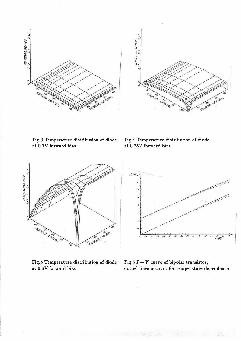
Fig.3 Temperature distribution of diode at 0.7V forward bias
Fig.5 Temperature distribution of diode at 0.8V forward bias
Fig.4 Temperature distribution of diode at 0. 75V forward bias
Fig.6 I - V curve of bipolar transistor, dotted lines account for temperature dependence


![Numerical Simulation of Heat Transfer During the Solidification … · · 2006-01-03Numerical Simulation of Heat Transfer During the Solidification of … , []} → → → →](https://img.dokumen.tips/doc/110x75/5adeb26e7f8b9ad66b8bded9/numerical-simulation-of-heat-transfer-during-the-solidification-simulation-of.jpg)