Embed Size (px)
Citation preview

Master’s thesis
Self-assembled SrRuO3 nanowiresthrough selective growth on DyScO3surface terminations
B. KuiperEnschede, October 9th 2009Applied PhysicsUniversity of TwenteFaculty of Science and TechnologyInorganic Materials Science
Graduation committeeProf. Dr. ing. Dave H.A. BlankProf. Dr. ir. H.J.W. ZandvlietDr. ir. G. KosterIr. J.L. Blok


Abstract
Self assembled SrRuO3 nanowires1 were grown selectively on one DyScO3(110) surface termi-nation by Pulsed Laser Deposition. This selective growth resulted in crystalline nanowires,typically 6 nm high, 80 nm wide and separated by a valley of 100 nm. The physical mechanismwhich drives the formation of these nanowires on mixed terminated substrates was studies usinga Solid-on-Solid model. SrRuO3 was assumed to have a high diffusivity on DyO terminatedareas compared to ScO2 and SrRuO3 covered areas. This resulted in nanowire formation onordered ScO2 terminated areas. Modelled growth on single DyO or ScO2 terminated substratesprovided an explanation for island and smooth growth respectively. Overall the model is ingood qualitative agreement with the deposited films, thus providing a mechanism for nanowiregrowth. A better understanding of the mechanism leads to more control over the properties anddimensions of these nanowires.
Nanowire physical properties were studied using Microwave Impedance Microscopy and 2-point electrical measurements. These indicate a clear contrast between the insulating DyScO3(110)substrates and conducting SrRuO3 wires.
1Cover image: Scanning Tunnelling Microscopy image of SrRuO3 nanowires on a DyScO3(110) substrate grownusing Pulsed Laser Deposition. Lateral dimension 1× 1 µm, wire height approximately 5 nm. More image detailsare depicted in figure 3.6
i


Table of contents
Abbreviations & symbols v
Introduction vii
1 Perovskite crystal growth 1
1.1 Perovskite crystals . . . . . . . . . . . . . . . . . . . . . . . . . . . . . . . . . . . 1
1.2 Crystal growth theory . . . . . . . . . . . . . . . . . . . . . . . . . . . . . . . . . 2
1.2.1 Atomistic view on crystal growth . . . . . . . . . . . . . . . . . . . . . . . 2
1.2.2 Growth modes . . . . . . . . . . . . . . . . . . . . . . . . . . . . . . . . . 3
1.3 Crystal growth by Pulsed Laser Deposition . . . . . . . . . . . . . . . . . . . . . 4
1.3.1 Reflection High-Energy Electron Diffraction . . . . . . . . . . . . . . . . . 4
1.3.2 Termination conversion . . . . . . . . . . . . . . . . . . . . . . . . . . . . 6
1.4 Crystal growth simulations . . . . . . . . . . . . . . . . . . . . . . . . . . . . . . 6
1.4.1 Solid-on-Solid model . . . . . . . . . . . . . . . . . . . . . . . . . . . . . . 6
1.4.2 Monte Carlo . . . . . . . . . . . . . . . . . . . . . . . . . . . . . . . . . . 7
2 Fabrication, characterization & simulation 9
2.1 DyScO3 substrate treatment . . . . . . . . . . . . . . . . . . . . . . . . . . . . . . 9
2.2 Pulsed Laser Deposition growth parameters . . . . . . . . . . . . . . . . . . . . . 10
2.3 Characterization equipment . . . . . . . . . . . . . . . . . . . . . . . . . . . . . . 11
2.3.1 Atomic Force Microscopy . . . . . . . . . . . . . . . . . . . . . . . . . . . 11
2.3.2 Microwave Impedance Microscopy . . . . . . . . . . . . . . . . . . . . . . 11
2.3.3 X-Ray Photoelectron Spectroscopy & X-Ray Diffraction . . . . . . . . . . 11
2.3.4 Nanomanipulator electrical measurements . . . . . . . . . . . . . . . . . . 12
2.4 Nanowire growth simulations . . . . . . . . . . . . . . . . . . . . . . . . . . . . . 12
2.4.1 Simulation parameters . . . . . . . . . . . . . . . . . . . . . . . . . . . . . 12
2.4.2 Modified Solid-on-Solid model . . . . . . . . . . . . . . . . . . . . . . . . . 13
2.4.3 Nanowire growth model . . . . . . . . . . . . . . . . . . . . . . . . . . . . 15
3 Experimental results 17
3.1 Acquiring mixed terminated DyScO3 . . . . . . . . . . . . . . . . . . . . . . . . . 17
3.2 PLD growth of SrRuO3 on DyScO3 . . . . . . . . . . . . . . . . . . . . . . . . . . 18
3.2.1 RHEED before, during and after growth . . . . . . . . . . . . . . . . . . . 19
3.2.2 Nanowire growth . . . . . . . . . . . . . . . . . . . . . . . . . . . . . . . . 21
3.2.3 Island growth . . . . . . . . . . . . . . . . . . . . . . . . . . . . . . . . . . 24
3.2.4 Combined growth patterns . . . . . . . . . . . . . . . . . . . . . . . . . . 25
3.2.5 Initial growth . . . . . . . . . . . . . . . . . . . . . . . . . . . . . . . . . . 25
3.3 DyScO3 termination control . . . . . . . . . . . . . . . . . . . . . . . . . . . . . . 26
3.3.1 SrRuO3 growth on ScO2 . . . . . . . . . . . . . . . . . . . . . . . . . . . . 27
3.3.2 SrRuO3 growth on DyO . . . . . . . . . . . . . . . . . . . . . . . . . . . . 28
iii

iv TABLE OF CONTENTS
3.4 SrRuO3 film properties . . . . . . . . . . . . . . . . . . . . . . . . . . . . . . . . . 293.4.1 SEM imaging & electrical measurements . . . . . . . . . . . . . . . . . . . 293.4.2 Conductivity mapping . . . . . . . . . . . . . . . . . . . . . . . . . . . . . 293.4.3 X-Ray spectroscopy . . . . . . . . . . . . . . . . . . . . . . . . . . . . . . 29
3.5 Model results . . . . . . . . . . . . . . . . . . . . . . . . . . . . . . . . . . . . . . 293.5.1 Nanowire growth . . . . . . . . . . . . . . . . . . . . . . . . . . . . . . . . 303.5.2 Island and smooth growth . . . . . . . . . . . . . . . . . . . . . . . . . . . 313.5.3 Combined growth . . . . . . . . . . . . . . . . . . . . . . . . . . . . . . . 31
4 Discussion: model versus experiments 35
4.1 The DyScO3 surface . . . . . . . . . . . . . . . . . . . . . . . . . . . . . . . . . . 354.2 SrRuO3 nanowire growth . . . . . . . . . . . . . . . . . . . . . . . . . . . . . . . 354.3 Physical mechanism . . . . . . . . . . . . . . . . . . . . . . . . . . . . . . . . . . 374.4 Model validity . . . . . . . . . . . . . . . . . . . . . . . . . . . . . . . . . . . . . . 38
5 Conclusions & Recommendations 39
Dankwoord 41
References 43
Appendices 45
A SOS Model code 45
B Additional results 47
B.1 Sc2O3 on DyScO3 growth . . . . . . . . . . . . . . . . . . . . . . . . . . . . . . . 47B.2 Dy2O3 on DyScO3 growth . . . . . . . . . . . . . . . . . . . . . . . . . . . . . . . 47B.3 X-Ray spectroscopy data . . . . . . . . . . . . . . . . . . . . . . . . . . . . . . . . 47B.4 Tuning SrRuO3 termination sensitivity . . . . . . . . . . . . . . . . . . . . . . . . 48B.5 Island shape control . . . . . . . . . . . . . . . . . . . . . . . . . . . . . . . . . . 48

Abbreviations & symbols
DyScO3 Dysprosium ScandateSrRuO3 Strontium RuthenateSrTiO3 Strontium Titanatea.u. Arbitrary unitsCM-AFM Contact Mode AFMIV curve Current Voltage curveMBE Molecular Beam EpitaxyMIM Microwave Impedance MicroscopyNC-AFM Non-Contact mode AFMPLD Pulsed Laser DepositionRHEED Reflection High-Energy Electron DiffractionSEM Scanning Electron MicroscopeSOS Solid-on-SolidSPM Scanning Probe MicroscopySTM Scanning Tunnelling MicroscopyTM-AFM Tapping Mode AFMu.c. Unit cellUHV Ultra High VacuumUPS Ultraviolet Photoelectron SpectroscopyXPS X-Ray Photoelectron SpectroscopyXRD X-Ray Diffractionα Characteristic jump distance [nm]γf Films surface free energy [J]γs Substrates surface free energy [J]τ Adatom residence time before desorption [sec]υ Hopping attempt frequency [Hz]a, b, c Lattice constants [nm]ap Psuedo-cubic lattice constant [nm]EA Activation energy for diffusion [eV]EB Step-up energy barrier per unit cell [eV/cell]ED Diffusion barrier [eV]EN Nearest neighbour bond energy [eV]ES Substrate bond energy [eV]Eadd Additional step-up energy barrier [eV]h SOS height [cell]hn SOS neighbour height [cell]k Hopping probabilityk0 Attempt frequency for hopping [Hz]kB Boltzmann’s constant [eV K−1]kx Hopping probability in direction x
v

vi TABLE OF CONTENTS
L Total SOS hopping probabilitylD Diffusion length [nm]lt Terrace width [nm]r Random number between 0 and 1S Normalized step densityT Temperature [◦C] or [K]
Introduction
Complex oxide a materials like DyScO3 and SrRuO3 are an interesting class of materials whichcomprise a large range of physical properties such as superconductivity (Y Ba2Cu3O7−x[1]),itinerant ferromagnetism (SrRuO3[2]) and ferroelectricity (PbZrxTi1−xO3[3]). Patterned mi-crostructures of these complex oxides, for example derived from sol-gels[4], create additionalapplications. Other techniques, for example Pulsed Laser Deposition[5] (PLD) allow for coher-ent growth of thin films consisting of these materials. During PLD growth the film thicknessand stoichiometry can be controlled artificially. Creating patterned PLD grown films results incoherently grown functional complex oxides which can be used in devices. For example con-ducting nanowires or ordered arrays of nanodots can be created[6]. The physical propertiesand nano structural control of these materials are being studied in great detail and are verypromising for future electronic applications. Moreover nanowires provide a method for studyingthe fundamental properties of materials at a small scale, for example by quantum confinementin one dimensional platinum chains[7].
In this report nanowire fabrication by self assembly is studied. Perovskite material SrRuO3
is grown on a DyScO3 substrate using PLD. A perovskite like DyScO3 can have two types ofsurface terminations: DyO and ScO2. SrRuO3 grows selectively on one of these terminations.This selective growth behaviour results in SrRuO3 nanowire formation when the substrate showsordered areas of both surface terminations. The goal of this research is to investigate the physicalphenomena which drive the self-assembly of SrRuO3 on DyScO3 chemical terminations duringPLD growth. A Solid-on-Solid (SOS)[8] model is used to simulate the growth on an atomic scalein order to better understand nanowire formation. The model is modified to allow for areas tohave different hopping barriers and it incorporates a basic form of hetroepitaxy.
In chapter 1 the theoretical background required to study growth behaviour of perovskitesduring PLD growth is discussed. An overview of the equipment and conditions used to fabricatethe films and the tools used analyse them is given in chapter 2. In this section the model isdescribed as well. The experimental results are given in chapter 3. In chapter 4 the modeland experimental data are compared and discussed. Chapter 5 contains the conclusions anda few recommendations. Appendix A includes part of the SOS C++ code used for simulatingwire growth, appendix B contains some additional data and a few types of interesting growthbehaviour, which could be studied in more detail in the future.
vii


Chapter 1
Perovskite crystal growth
In this chapter the theoretical background required to study nanowire growth during PulsedLaser Deposition (PLD) is explained. Since both SrRuO3 and DyScO3 are perovskite crystals,first perovskite crystal and the kinetic model which describes their behaviour during growthare discussed. Secondly PLD-RHEED growth is explained, the RHEED measurements arecompared with theoretical growth modes. Finally the theory behind Solid-on-Solid Monte Carlosimulations is discussed.
1.1 Perovskite crystals
Both DyScO3 and SrRuO3 are complex oxide materials which are part of the perovskite ABO3
crystal class. A cubic perovskite is drawn schematically in figure 1.1a, it contains oxygen anionsand two types of cations of different size, A and B. The cations can have a charge ranging from+1 to +5, for example A2+B4+O6−
3. The B-site cation is surrounded by an oxygen octahedron,
drawn in figure 1.1a as well. ABO3 perovskite materials consist of alternating layers of AO andBO2, drawn schematically in figure 1.1b. If the A-site cation has a charge of 2+ and the B-sitecations are 4+, these layers are charge neutral. In the case of (A3+O)+, (B3+O2)
− the layersare polar. DyScO3 is a 3+/3+ perovskite.
(a) Cubic ABO3 (b) Layers
A-site
B-site
Oxygen
Figure: 1.1: Cubic ABO3 perovskite (a) and alternating layers AO, BO2, AO (b) aredrawn schematically
DyScO3 is not cubic, it has a distorted orthorhombic structure with Sc-O-Sc angles be-tween 139-144◦[9]. The orthorhombic structure contains four formula units per full cell. Anorthorhombic DyScO3 structure is drawn schematically in figure 1.2. The Pnma lattice con-stants of DyScO3 are a = 0.5720 nm, b = 0.5442 nm and c = 0.7890 nm which correspond toa psuedo-cubic lattice constant of ap = 1
2
√a2 + b2 ≈ c
2= 0.3945 nm. This pseudo-cubic cell is
drawn in figure 1.2 as well. DyScO3 (110) direction has a square lattice with lattice constant
1

2 CHAPTER 1. PEROVSKITE CRYSTAL GROWTH
ap. One must keep in mind that the DyScO3 (110) pseudo-cubic cell is only square in the (110)direction not in other directions. All Figures and text in this report refer to the pseudo-cubiccrystal where the pseudo-cubic c-axis lies parallel to the growth direction (110) unless specificallydefined otherwise.
Figure: 1.2: Orthorhombic DyScO3 crystal structure (Pnma) showing two psuedo-cubicsubcells inside the orthorhombic unit cell. [9]
SrRuO3 also is an orthorhombic perovskite with psuedo-cubic lattice constant ap = 0.393 nm.The lattice mismatch between DyScO3 and SrRuO3 is small [9], which allows for coherent growth.Another close match to SrRuO3 is SrTiO3 (cubic a = 0.3905 nm) which is commonly used asa substrate material. The SrRuO3 strain with respect to DyScO3 is tensile while the strain iscompressive with respect to SrTiO3. The topmost layer of a perovskite crystal can be either oneof the alternating layers. This surface termination is known to vary locally on the substratessurface. In the case of SrTiO3, SrO can be chemically etched[10] using a buffered HF solutionto acquire only TiO2 termination. During the final stages of this master project a method tocreate single terminated DyScO3 surfaces was developed using a NaOH treatment [11].
1.2 Crystal growth theory
Crystals can be created artificially, using for example PLD. During PLD growth material isevaporated onto a substrate. What happens at the substrate depends on many factors, like thetype of substrate and the type of material being evaporated, but also the temperature and therate at which the material is evaporated. Two ways of describing crystal growth are possible.In equilibrium the surface morphology can be described by thermodynamics[12]. However todescribe nanowire formation during growth, not in equilibrium, a more detailed method foranalysing surfaces is required. Kinetic theory provides this description of the physical mechanismwhich governs nanowire formation.
1.2.1 Atomistic view on crystal growth
Kinetic theory studies the motion of single atoms or individual perovskite unit cells on a crystalsurface. A crystal surface is vicinal, in other words it is tilted with respect to the desired crystaldirection by a certain miscut angle. This tilt results in steps of unit cell (u.c.) height separated

1.2. CRYSTAL GROWTH THEORY 3
by flat terraces. Such a terrace and all possible movements for a single cell are depicted in figure1.3. Cells or atoms arrive at the surface and can adsorb (stick) to the surface (a,f). Once atthe surface they can diffuse (b), nucleate (c), form islands (d), detach from islands (e), stepup/down islands or steps (g) or detach from the surface (j).
Figure: 1.3: Schematic representation of the atomic process during growth: (a) deposi-tion of an adatom on a terrace; (b) diffusion of an adatom on the terrace;(c) nucleation of two adatoms; (d) attachment of adatoms at an island; (e)detachment of atoms from an island; (f) deposition of an adatom or clusteron top of island; (g) step-down diffusion of an adatom; (h) diffusion alonga stepedge; (i) attachment of an adatom at a step; (j) desorption from aterrace. [13]
In the kinetic model surface morphology evolution is determined by a surface diffusion coeffi-cient DS which relates the diffusion distance lD to τ , the adatom residence time before desorptionor incorporation at a step edge. This relation is given by equation 1.1.
lD =√
DSτ (1.1)
The expression for the surface diffusion coefficient is given by equation 1.2. Where υ is thehopping attempt frequency, α the characteristic jump distance, kB Boltzmann’s constant and Tthe temperature. EA represents the activation energy for diffusion.
DS = υα2e
(
−EA
kBT
)
(1.2)
1.2.2 Growth modes
From a thermodynamic point of view two types of growth can be distinguished depending onthe relationship between the substrate surface free energy γs and the film surface free energy γf .If γs > γf three dimensional growth occurs also known as Volmer-Weber growth mode, depictedschematically in figure 1.4a. If γs < γf the substrate is easily wetted by the film resulting in 2Dlayer-by-layer growth also known as Frank- van der Merwe growth mode(b). A combined growth2D/3D growth mode also exists when growing on misfit substrates called Stranski-Krastanov(c).Two dimensional growth can be divided into two group by the kinetic model. If the diffusiondistance lD is small compared to the step width lt atoms will coalesce 1.3(c),(d) to form islandson the terrace, growing in a layer-by-layer fashion (a). If lD is large compared to lt adatomswill nucleate on the step edges instead of forming islands (d). This growth mode is referred toas step-flow-growth.

4 CHAPTER 1. PEROVSKITE CRYSTAL GROWTH
Figure: 1.4: Surface morphology evolution scenarios during growth: (a) three-dimensional island growth, Volmer-Weber; (b) two-dimensional layer-by-layer growth, Frank-van der Merwe; (c) Stranski-Krastanov growth (d)two-dimensional step flow growth. [13]
1.3 Crystal growth by Pulsed Laser Deposition
Pulsed Laser Deposition (PLD) is one of the physical vapour deposition techniques used to growperovskite thin films. Material is ablated from a target and transferred to a substrate. Boththe target and substrate material are placed in a vacuum chamber. The background pressureand gas mixture in the chamber can be controlled and monitored. Material is ablated from thetarget by a high intensity laser. The laser pulse generates a dense plasma of target materialwhich expands away from the target towards the substrate. At the substrate part of the arrivingmaterial will adsorb onto the substrate. The substrate can be heated to allow for better stickingof the arriving species. The amount of material ablated from the target depends on the laserenergy and the spot size. The background pressure, target-substrate distance and the substratetemperature determine the amount of material deposited on the substrate by each pulse.
A schematic drawing of a PLD system is depicted in figure 1.5. A target holder capable ofholding multiple targets allows for sequential deposition of different materials. During growththe substrates surfaces is monitored using an electron beam, RHEED[5]. The RHEED tube andcorresponding CCD-camera are drawn as well.
1.3.1 Reflection High-Energy Electron Diffraction
Reflective High Energy Electron Diffraction (RHEED) can be used during PLD growth. TheRHEED signal can be recorded over time during deposition, because RHEED is used with alow angle of incidence. Due to this low angle of incidence RHEED is very surface sensitive andallows for in-situ monitoring of the surface during growth. The diffraction pattern as a result ofinterference of electrons with the crystal lattice is indicative of the crystal surface. An example2D RHEED pattern is depicted in figure 1.6a. The specular spot is indicated by a square box.

1.3. CRYSTAL GROWTH BY PULSED LASER DEPOSITION 5
Figure: 1.5: Schematic impression of a Pulsed Laser Deposition set-up. A laser beamablates material from a target onto a substrate. During growth the sub-strates surface is monitored using RHEED[13].
This patterns shows the direct beam on the left side and several 2D spots. Figure 1.6b showsan example 3D RHEED pattern showing many spots.
(a) 2D (b) 3D
Figure: 1.6: Example 2D(a) and 3D(b) RHEED patterns. The square box indicates thespecular spot.
The growth modes depicted in figure 1.4 can be distinguished by the RHEED signal. Incase the samples surface contains small islands the electron beam will penetrate the islandsand fulfilment of the Bragg condition leads to additional spots, called 3D spots. These spotsindicated Volmer-Weber like growth during PLD.
In case of layer-by-layer growth, the surface roughness changes while the RHEED patternremains 2D. After half a layer of material is deposited, the film is relatively rough. Completion ofa monolayer will results in a smooth film and a maximum specular spot intensity. So the growthof a single monolayer is indicated by one oscillation. The RHEED signal can be used to tunefilm thickness during growth. Directly after each laser pulse adatoms are distributed randomlyover the surface and the specular spot intensity drops down due to the large amount of unit cellhigh steps caused by the newly arrived atoms. The signal recovers quickly while atoms diffuseand form islands. In case of step-flow growth no islands are formed and the surface roughnessdoes not change, resulting in a steady state RHEED signal. This intensity drop and recoveryafter each laser pulse is much more pronounced in step-flow growth. The RHEED recovery timeis indicative of the adatom residence time τ used in equation 1.1. Surface roughness can alsobe described in terms of step density. A rough surface has many steps compared to a smooth

6 CHAPTER 1. PEROVSKITE CRYSTAL GROWTH
surface. A high step density corresponds to a rough surface and a low specular spot intensity.
1.3.2 Termination conversion
During deposition the target material is converted into a plasma of individual atoms while onlycomplete perovskite cells are expected to adsorb to the substrate surface. In case of SrRuO3
one of the species, RuOx, is very volatile. It is easy to imagine if this volatile species is presentat the topmost layer, it could evaporate. Rijnders et al. [14] have shown this indeed happensduring growth of the first few layers of SrRuO3 on TiO2 terminated SrTiO3(001). During growththe surface termination switches from B-site TiO2 to A-site SrO. The time required to switchis twice the time required to create a single layer. When two complete cells or four half unitcells are expected to grow only three half-unit cells grow. This was registered using RHEED,the period of the first oscillation was twice the normal period. This behaviour is expected tobe related to SrRuO3 and therefore is also expected for growth of SrRuO3 on ScO2 terminatedDyScO3. Therefore it could provide information about which termination nanowires prefer togrow on.
1.4 Crystal growth simulations
The kinetic model described in section 1.2.1 considers individual movement of unit cells ona crystal surface. These movements depicted in figure 1.3 can be simulated. A method forsimulating growth during vapour deposition techniques is described in section 1.4.1. This modelwas used to simulate nanowire growth in this report. Only features which will be applied tothese specific simulations will be discussed.
1.4.1 Solid-on-Solid model
To simulate nanowire growth a Monte Carlo algorithm is applied to the kinetic theory describedin section 1.2.1. Monte Carlo methods rely on repeated random sampling to study the behaviourof systems with many coupled degrees of freedom. This combination of Monte Carlo and kinetictheory is referred to as a Solid-On-Solid[15] (SOS) model. Perovskite unit cells are treated assingle entities on a matrix grid of possible positions. Physically similar to the crystal positionson a crystal surface. The cells are allowed to diffuse according to kinetic theory. Only one cellmoves at a time, selected by a random pick. The chance a cell is selected to move is proportionalto the diffusion coefficient given by equation 1.2. After a cell has moved the next cell is selectedto move. This selection process is repeated for as long as desired.
SOS assumes a n × m grid of possible sites, each site is able to contain single unit cellsstacked upon each other. Cells are only allowed to hop to neighbouring sites. In this report aSOS neighbour is defined by a simple square lattice. The hopping probabilities k is given by anArrhenius type equation, like equation 1.2, more specifically given in equation 1.3 where k0 isthe attempt frequency for hopping.
k = k0e
(
−ED
kBT
)
(1.3)
The diffusion energy ED consists of several individual energy barriers. ES is the of the energybarrier due to bonding with the substrate and EN is the nearest-neighbour bond energy. Thenearest neighbour bond energy is multiplied by the number of nearest-neighbour bonds n beforebeing added to diffusion energy, as given by equation 1.4. The number of nearest-neighboursis calculated by comparing the height of one grid site with its four neighbours. In this SOSmodel ideal sticking of arriving atoms is assumed and no re-evaporation is allowed. Once aunit cell has arrived at the substrate it must diffuse 1.3(b) until it nucleates 1.3(c) or becomes

1.4. CRYSTAL GROWTH SIMULATIONS 7
incorporated bellow a new layer of arriving cells 1.3(f). Atomic processes desorption 1.3(f) andcluster diffusion or deposition 1.3(b),1.3(g) are not considered for nanowire growth simulations.
ED = ES + n · EN (1.4)
RHEED intensity oscillations can also be simulated using a SOS model. The step density canbe calculated from the models matrix grid, using equation 1.5. A large step density correspondsto a rough surface and would be indicated by a low RHEED signal. The RHEED intensityevolution is proportional to 1 minus the normalized step density.
S =1
n × m
∑
i,j
|hi,j − hi,j+1| cos φ + |hi,j − hi+1,j | sin φ (1.5)
To simulate RHEED monitored growth using a SOS model each laser pulse is simulated by arandom deposition of a certain number of unit cells. After this pulse all hopping probabilities ofeach grid position in all four hopping directions are calculated and stored. The cells are allowedto diffuse for a certain amount of time or for a fixed number of simulation steps using the MonteCarlo method described in section 1.4.2. During diffusion surface morphology and step densityevolutions are recorded. After diffusion a new random deposition of cells takes place. Thisprocess continues until the desired amount of cells are deposited.
1.4.2 Monte Carlo
Unit cell or adatom diffusion is simulated by simply selecting one diffusion process or event. Thechance an event is selected depends on its hopping rate. Events with a higher hopping rate havea higher hopping probability. An event is selected by calculating the total hopping probability Lby summing up all individual hopping rates for every grid site (i, j) and every hopping direction(x), L =
∑
i,j
∑
x kx. A random number 0 < r < L is selected and the event corresponding tothis random number is selected. This event selection process is drawn schematically in figure 1.7.An example grid is drawn as well, showing the periodic boundary conditions. Event selectionis repeated millions of times during a simulation. The implementation of event selection is ofgreat importance for minimizing simulation time. A binary chop algorithm is used[16] to selectevents. Binary chop divides all possible events drawn in figure 1.7 into two groups and calculatesthe total hopping rate of the first group L1. It checks if the selected random number within thefirst group: r < L1. If it is in the first group the process is repeated within the first group, if notit is repeated within the second group. Finally it will find a group consisting of only one eventand the event is selected. To decrease simulation time, this binary chop from all possible eventsis divided into two parts, known as fast Monte Carlo [16]. All events are divided into groups.For instance the left quarter of the matrix grid is chosen as one group of events. First a groupis selected by binary chop and secondly an event inside the group is selected. A more detaileddescription of this fast Monte Carlo method is given by Maksym [16].

8 CHAPTER 1. PEROVSKITE CRYSTAL GROWTH
Figure: 1.7: Example 5x5 grid indicating hopping directions up, down, left, right fromgridsite(2,0). Periodic boundary conditions are used, depicted for hoppingto the left. For each possible direction a rate kx is calculated. All ratessummed up and by picking a random number 0 < r <
∑
kx an event isselected by means of a binary chop algorithm.

Chapter 2
Fabrication, characterization &
simulation
This chapter contains an overview of the experimental conditions and equipment used to fabri-cate nanowires and study their properties. The final section of this chapter contains a detaileddescription of the modified SOS model used to simulate SrRuO3 growth on DyScO3.
2.1 DyScO3 substrate treatment
The DyScO3 substrates used for this research were manufactured by CrysTec GmbH using aCzochralski process. This method results high crystallinity and low mosaicity compared to, forexample commonly used SrTiO3 substrates.
(a) As-received (b) After annealing
Figure: 2.1: TM-AFM 10×10 µm images of a DyScO3 substrate before and after an-nealing for 4 hours at 1000 ◦C on a low miscut substrate. Images (a) showsa low miscut sample before annealing. After annealing the steps order instraight lines (b), however unit cell high islands are still present at thesurface.
The received substrates have been cleaned with acetone and ethyl-ethanol before being an-nealed at 1000 ◦C under oxygen flow for various periods of time, ranging from 30 minutes to85 hours. Example as-received and annealed DyScO3 substrate TM-AFM images are depictedin figure 2.1. The as-received (a) image shows the substrates surface before annealing, the stepedges are very rough. Image (b) shows a TM-AFM image of the same sample after annealingfor 4 hours at 1000 ◦C. Due to the low miscut of this sample, resulting in a step width of 1000
9

10 CHAPTER 2. FABRICATION, CHARACTERIZATION & SIMULATION
nm, the annealed substrate still shows unit cell high islands on the terraces.1. Figure 2.2 showstypical AFM images of an atomically smooth DyScO3 surface without these islands or holesindicating unit cell high steps and a stepwidth of approximately 300 nm.
(a) Height image
0 0.5 1 1.5 20
0.5
1
1.5
2
2.5
3
x (µm)
heig
ht (
nm)
300 nm
0.4 nm
(b) Profile
Figure: 2.2: TM-AFM 2×2 µm image with a sharp tip recorded at a scan speed of 1 Hzand a line profile averaged over 5 lines. RMS roughness is below 0.05 nmindicating an atomically smooth surface
Four hours annealed DyScO3 substrates with a miscut angle above 0.07◦ show atomicallysmooth surfaces with unit cell high steps and straight step edges. Typical peak to peak surfaceroughness is below 0.2 nm. For SrTiO3 it is assumed[17, 13] that sodium contamination at thesurface is likely to cause this roughness. Since DyScO3 has polar layers it seems even morelikely to attract these contaminations. An example TM-AFM image recorded with a sharp tipis depicted in figure 2.2.
2.2 Pulsed Laser Deposition growth parameters
All films are grown using Pulsed Laser Deposition (PLD), described in section 1.3. A KrFexcimer laser with a wavelength of 248 nm was used. Maximum pulse energy of the laser is 1000mJ and minimal pulse duration 25 ns. The parameters used for growing SrRuO3 on DyScO3
are presented in table 2.1. Sc2O3 and Dy2O3 growth parameters are shown as well. Depositionfrom these targets on DyScO3 substrates was done in order to manually create ScO2 and DyOsurface terminations.
SrRuO3 Sc2O3 Dy2O3
Temperature (setpoint) 750 950 950 [◦C]Fluency 2.1 2.1 2.1 [J/cm2]
Mask size 60 20 60 [mm2]Laser repetition rate 1 1 1 [Hz]
Target substrate distance 50 50 50 [mm]Pressure 0.3 0.01 0.01 [mbar]
Gas mixture O2/Ar 50 100 100 O2[%]
Table 2.1: Pulsed Laser Deposition growth parameters
1These unit cell deep holes or islands and their evolution during annealing is described in more detail forSrTiO3 substrates[13].

2.3. CHARACTERIZATION EQUIPMENT 11
2.3 Characterization equipment
Most films have been grown in the COMAT system. This system connects 4 UHV chambers witha central distribution chamber. It allows for samples to be transferred under UHV conditionsfrom a PLD-RHEED system to a sputter chamber, a SPM chamber and a XPS/UPS chamber.
2.3.1 Atomic Force Microscopy
In order to investigate the surface morphology of both substrates and films, several types ofscanning probe techniques were used. For analysing substrates and films outside vacuum condi-tions, either the Veeco MultiMode SPM or the Veeco Dimension Icon AFM was used in air andat room temperature. Both can be operated in either Contact-Mode (CM) or Tapping-Mode(TM). For this work CM tips with a thickness of 2 ± 1 µm, a length of 450 ± 10 µm and awidth of 50± 7.5 µm and TM tips with a thickness of 4± 1 µm, a length of 125± 10 µm and awidth of 30 ± 7.5 µm were used. The force constants are 0.02 − 0.72 N/m and 10 − 130 N/mrespectively and the TM-tips had a frequency of 204− 489 kHz. A third SPM system, OmicronMultiMode SPM, is connected via a UHV connection to the PLD chamber and is able to doCM, Non-Contact mode (NC) and STM in vacuum conditions.
Since DyScO3 substrates are insulating, AFM is the main tool to investigate surface mor-phology. Both CM and TM AFM have been used to study the substrates after annealing. Themain difference between these modes of operation is the force regime in which the tip-sampleinteraction takes place.
For CM-AFM the tip is in contact with the surface and de tip deflection in the z directionis fed trough a feedback loop which effectively keeps tip height constant. The repulsive forcesinvolved are in the nano Newton range. The tip can also show deflection in the xy-plane, thetip twists as a result of scanning it across the surface. Measuring this type of deflection is calledlateral force microscopy or friction force microscopy. In case of scanning perovskite materials,both terminations can have a different tip-sample interaction strength which will give rise tolateral force contrast. Figure 3.2 shows an example CM-AFM image with a friction map.
For NC-AFM and TM-AFM an oscillating cantilever is brought into close contact with thesubstrate. A feedback loop is applied to either the amplitude of the oscillation or the frequency.Typical forces involved in NC-AFM are in the pico Newton range, for TM-AFM the forcesinvolved are higher and approach the repulsive regime of CM-AFM. Both TM-AFM and NC-AFM allow for phase imaging. Phase imaging registers the phase shift in the measured signalcompared to the drive signal. A phase shift can be induced by areas of different adhesion ordifferent friction, thus providing information similar to lateral force microscopy.
2.3.2 Microwave Impedance Microscopy
Microwave Impedance Microscopy[18] (MIM) is a technique based on AFM. A modulated mi-crowave (1GHz) signal is applied to a specially fabricated AFM tip. This method provides anabsolute measurement of the local dielectric properties. Both the real (MIM-R) and imaginary(MIM-C) components of the tip impedance are recorded. It can be operated CM-AFM andTM-AFM.
2.3.3 X-Ray Photoelectron Spectroscopy & X-Ray Diffraction
X-Ray Photoelectron Spectroscopy (XPS) spectra for several samples were recorded using anOmicron EA125 Analyser and an Cu Kα1 x-ray source part of the COMAT system. X-RayDiffraction (XRD) was used to measure substrate miscut prior to annealing and to check crystalquality. XRD was performed ex-situ on a Bruker D8 XRD.

12 CHAPTER 2. FABRICATION, CHARACTERIZATION & SIMULATION
2.3.4 Nanomanipulator electrical measurements
In order to measure the transport properties of the nanowires, a Zyvex S100 nanomanipulatorwas combined with a Keithley 4200-SCS Semiconductor Characterization System. These mea-surements were performed during SEM imaging using a Jeol JSM-6490 SEM. This system allowsfor positioning probes onto features down to 100 nm in size.
2.4 Nanowire growth simulations
A SOS model, described in section 1.4.1 was written in C++ programming language, usingMicrosoft Visual C++ 9.0 and compiled for windows 32bit platforms. C++ allows for easyimplementation of well known classes and routines. Most of the classes used are part of theROOT tool kit2.
2.4.1 Simulation parameters
Using a SOS model many PLD growth modes and corresponding RHEED signals can be sim-ulated. For example the RHEED intensity drop and recovery after each laser pulse is clearlyvisible in all simulations. Island growth and step-flow growth can be simulated by choosingthe appropriate parameters. A transition from island shaped layer-by-layer growth to step-flowgrowth can be induced by either increasing the temperature or decreasing the stepwidth. Thelatter is used to verify the models behaviour, described in more detail in section 2.4.1. Anoverview of SOS parameters is shown in table 2.2.
SOS is just a model and results must be interpreted keeping in mind some effects might becaused by the model itself and are not related to any physical phenomena. For example, thegrid size parallel to the step edges is reduced to decrease simulation times. Periodic boundaryconditions are used to model adatoms traversing the grid boundary. On a vicinal substrateboth sides of the grid perpendicular to the step direction have a different substrate height. Acorrection must be applied to compensate the height difference between both sides of the grid.In the direction parallel to the step edges the grid size is reduced, sometimes it is reduced belowthe diffusion length, thus limiting the diffusion length. Since the model is created for nanowiregrowth simulations, the exact behaviour in the direction parallel to the step edges, also parallelto the wires is not of interest. As a result of limiting the diffusion length on top of the wires byreducing the grid size, step density oscillations might be visible when growing step-flow like ontop of nanowires.
Another intrinsic problem is caused by reducing the simulated environment to two dimen-sions. Only the topmost atom on every grid site is allowed to diffuse. Atoms are only allowedto sit on top of other atoms. No 3D overhang is allowed and only 2D growth modes can besimulated easily. In the case of nanowire growth which is 3D, adatoms can hop on and off islandswithout any influence of the height difference they must overcome. This was compensated for bya method described in section 2.4.2, basically introducing a barrier for hopping up a nanowireor island depending on the height difference.
Rijnders [19] determined the diffusivity of SrRuO3 on SrO terminated SrRuO3 and found acorresponding activation energy of 1.0 ± 0.2 eV. The SOS settings used by Rijnders [19] weremodified slightly for SrRuO3 on DyScO3 growth simulations. The temperature used for nanowiresimulations is lowered to save simulation time3. This resulted in a step-flow to layer-by-layer
2The ROOT system provides a set of Object-Oriented frameworks with all the functionality needed to handleand analyse large amounts of data in a very efficient way. Developed at CERN in the context of the NA49experiment. URL: http://root.cern.ch/
3A 512 × 128 simulation at 700 ◦C required 1-2 weeks of simulation time, while at 300 ◦C 12 hours wassufficient.

2.4. NANOWIRE GROWTH SIMULATIONS 13
Rijnders [19] Example Nanowires
Temperature 600 700 300 [◦C]Attempt frequency k0 10 10 10 [THz]
Grid size (n × m) 490 × 490 512 × 128 512 × 128 [pixels]ES 0.75 0.75 0.55-0.85 [eV]EN 0.60 0.65 0.25 [eV]
Pulses per monolayer 20 30 30 [#]Pulse repetition rate 2 4 4 [Hz]
Stepwidth 23-51 23,152 68,102 [nm]
Table 2.2: SOS model growth parameters
growth transition on top of the nanowires, but did not alter the formation of the nanowires sincethe diffusion length remained larger than the nanowire spacing.
Layer-by-Layer to step-flow growth transitions
Figure 2.6 shows SOS results for a layer-by-layer to step-flow growth mode transition as a resultof changing the substrate miscut angle from 0.15◦ to 1.00◦. Rijnders [19] showed this transitionoccurs using the following parameters: ES = 0.75 eV and EN = 0.60 eV . The parameters usedfor this example are depicted in table 2.2.
Figure 2.6a shows a layer-by-layer growth mode. Islands form and coalesce to form a newlayer of material after deposition of 30 pulses. This is clearly visible in the correspondingstep-density function depicted in figure 2.6c (light), which shows oscillations. 2.6b shows a step-flow-growth mode, no islands form and the step density in figure 2.6c (dark) remains constant4.
2.4.2 Modified Solid-on-Solid model
Normally SOS models are used to simulate 2D growth modes, since most 3D growth modesare more easily described by thermodynamics. To simulate the formation of nanowires a 3D-like growth mode must take place. To allow wired growth through diffusion, step-up diffusionmust be allowed. In most SOS models step up diffusion is specifically prohibited. If step-updiffusion is prohibited or energetically unfavourable, step-flow growth will occur. Wire growthsimulations thus require step-up diffusion to be energetically favourable. The difference betweenstep-flow and step-up growth is schematically drawn in figure 2.3. In case it is energeticallyunfavourable to hop onto steps the film remains smooth (left). If adatoms hop up steps on thesurface nanowires start to grow in heigth (right).
Mixed termination anisotropy
In order to grown nanowires the substrates mixed termination must make it energeticallyfavourable to hop up steps. Therefore mixed termination is simulated by creating orderedareas of different diffusion barrier EA
S and EBS while keeping the nearest neighbour interaction
term constant. An higher ES value decreases the hopping rate, this lowers the diffusivity. Thefirst layer of adatom always replicates the ordered areas if diffusion length is large enough foradatoms to reach the area with the highest ES value. The second layer of cells must overcomean addition nearest neighbour bond to jump up the first layer. To allow for nanowires to growin height on areas where ES = EB
S and not in width equation 2.1 should hold. If the differencebetween both sides of equation 2.1 is small, the growth rate plays a role as well. If a new pulse of
4The variations in the step density function for step-flow growth are caused by the finite simulation grid andboundary effects. Steps leave and appear on the simulation grid, causing minor changes in the step density.

14 CHAPTER 2. FABRICATION, CHARACTERIZATION & SIMULATION
Step−upStep−flow
A−site
B−site
New adatom
Adatom
Figure: 2.3: Step flow vs step up diffusion indicating that after completion of one layerof adatoms on top of B-site terminated areas either step-flow growth (left)or step-up growth (right) can occur. The balance between both depends ofthe difference in hopping barrier for both situations, given in equation 2.1.
material is applied before the previous adatoms have reached areas with a high hopping barrier,these new adatoms could hinder the previous adatoms from reaching these areas, by providingextra nearest neighbour bonds..
EAS + EN < EB
S (2.1)
Hetroepitaxy anisotropy
The model simulates SrRuO3 growth on DyScO3. The hopping barrier for hetroepitaxy: SrRuO3
on DyScO3 is expected to be different than the barrier for homoepitaxy SrRuO3 on SrRuO3.This can be introduced by chancing the ES value after growth of one cell[20]. Figure 2.4 gives anexample of such hetroepitaxy. In this example the hopping barrier is lowered locally from 0.75eV to 0.45 eV. This induces a transition from layer-by-layer to step-flow growth after completionof the first monolayer which is clearly visible in the calculated step density values. The nanowiresare simulated by creating an area with a low EA
S value and a high EBS value. The EA
S area hasa high diffusivity and cells prefer to stick at areas with EB
S . The difference between EBS and the
films ES value are assumed to be small. Different types of nearest neighbour interactions[20]are not studied in this report, most neighbours are SrRuO3 except for the substrate step edges.
Step-up barrier
Cells are allowed to hop onto steps, islands and wires independent of the height difference.Without mixed termination anisotropy such a jump would be unfavourable anyway, since anearest neighbour bond must be broken to make the jump. This neighbour is not regainedafter the jump. Also a additional Ehrlich-Schwoebel barrier positive or negative [21] could beincluded. This could prevent or enhance the chance of an atoms stepping down a step. Sincewire growth due to mixed termination anisotropy is studied no additional Erhlich-Schwoebelbarrier is added, which could drastically alter the growth behaviour.
Diffusion along the nanowire or island sides is no different from diffusion along the surface,gravity does not play a role in this force regime. Physically an atom stepping up a nanowire

2.4. NANOWIRE GROWTH SIMULATIONS 15
0 5 10 15 20 25 30Time (sec)
inv.
ste
p de
nsity
(a.
u.)
Figure: 2.4: Simulated increased diffusivity indicated by a change from oscillatingRHEED to steady-state RHEED after completion of the 1th layer. Thechange is induced by a lowering of the energy barrier ES by 0.3 eV atexample SOS condition shown in table 2.2.
should hop up the side of the nanowire step by step. To incorporate this into the model anadditional barrier is added depending on the number of steps required to hop onto a nanowire.This barrier scales with the wire height and is given by equation 2.2. This equation holds onlyfor hn > h where h is the original atom height and hn the height of the neighbour the cell isjumping towards. Equation 1.4 gains an additional term: ED = ES + n · EN + Eadd.
Eadd = EB(hn − h) (2.2)
2.4.3 Nanowire growth model
Mixed termination anisotropy, hetroepitaxy and an additional step-up barrier described aboveare added to the standard SOS model to simulate wire growth. A-site and B-site choice isarbitrary in the model. The energy barrier for diffusion related to the surface interaction at A-site termination is chosen relatively low, EA
S =0.55 eV to force adatoms on A-site to step-flow atthe selected temperature. The surface related energy barrier on B-site is chosen to be EB
S =0.85eV. The adatom-adatom surface interaction hopping barrier is chosen slightly lower, ES=0.75eV. A nearest-neighbour interaction energy of EN=0.25 eV is used. The step-up barrier increaseswith height EB=0.01 eV/cell. An overview of the important energy barriers is depicted in figure2.5. The choice of these parameters is based on the settings proposed by Rijnders [19] andMolecular Beam Epitaxy (MBE) parameters used by Vvedensky et al. [22]5.
ED = EAS + EN
ED = EAS + EN + 3EB
ED = ES + 2EN
ED = EASED = EB
S
B-Site
B-SiteA-Site
A-Site
ES = 0.75 eV
EAS = 0.55 eV
EBS = 0.85 eV
EN = 0.25 eV
EB = 0.01 eV
Figure: 2.5: Overview of typical 2D SOS energy barriers
5Parameters used by Vvedensky et al. [22]: k0=1013 Hz, ES=1.3 eV, EN=0.25 eV and a temperature between0 and 500 ◦C.

16 CHAPTER 2. FABRICATION, CHARACTERIZATION & SIMULATION
(q) 0.15◦ vicinal surface (r) 1.00◦ vicinal surface
0 5 10 15 20 25 30 35 40Time (sec)
Inve
rse
step
dens
ity (
a.u.
)
0.15 miscut1.00 miscut
(s) Corresponding simulated RHEED oscillations
Figure: 2.6: Step-flow to layer-by-layer growth transition for two miscut angles usingexample growth parameters depicted in table 2.2. Images correspond todeposition of 1, 15, 30, 45, 60, 75, 90, 105 and 120 pulses from top tobottom.

Chapter 3
Experimental results
This chapter gives an overview of all experiments relevant for discussion in chapter 4. First allphysical experiments, such as PLD growth and AFM measurements are shown and explained.Finally the SOS model results are listed and clarified.
3.1 Acquiring mixed terminated DyScO3
The first step for growing nanowires is substrate treatment. Since the wires are expected togrow on one of the DyScO3 chemical terminations, this treatment is a crucial step for growingnanowires. The mixed termination ratio was determined using lateral force microscopy. It wasnot always straightforward to record such a lateral force/friction contrast. Several factors makeit difficult to detect mixed termination. The quality of the AFM tip and the alignment of theAFM laser should be optimized. Since optimization is just a matter of time and effort, the actualdifficulty might be surface contaminations. For SrTiO3 sodium and water contaminations areknown to disturb the AFM measurement [13],[17]. DyScO3 has polar layers and different surfacetermination might be more sensitive to different kinds of contaminations. These contaminationscould equalize the surface friction contrast. Contaminations are easily obtained by humanperspiration on beakers or tweezers. The contaminations are difficult to clean chemically. Above500 ◦C in vacuum these contaminations sublimate[17] and thus should not influence the SrRuO3
growth, but might make recording a friction contrast more difficult.The vicinal mixed terminated substrates theoretically allow for three different kinds of or-
dering. These different kinds of stacking are depicted in figure 3.1. Option (a) results fromcontinuous half unit cell high steps, resulting in an alternating friction contrast (inset). Option(b) depicts half unit cell steps down followed by full unit cells step down. This stacking wouldresult in a doubled period of the friction contrast. Stacking option (c) shows half unit cell stepsup followed by 1.5 unit cell steps down, resulting in friction contrast similar to staking (a).
The influence of the anneal time on the mixed termination ratio was measured by annealingthree samples for different periods of time, 30 minutes, 4 hours and 8 hours at 1000 ◦C. Thesubstrates were prepared as described in section 2.1. After annealing the surface morphologywas checked using CM-AFM. The AFM height and friction force images are depicted in figure3.2. The samples were cut from the same 10x10mm, 0.1 ◦miscut substrate. The miscut directionand stepwidth varied slightly over the substrates surface. In general the steps run parallel to abulk crystal edge. The series shows an straightening of the step edges between 30 minutes to4 hours of annealing. The 8 hours sample shows little or no mixed termination. The frictioncontrast around the step edge of the 8 hours sample is likely to be caused mainly by the stepedge and not by mixed termination. The inverted colour of the friction map of sample (c) iscaused by scanning across the substrate in an other direction compared to the first two frictionmaps. For the 30 minutes and the 4 hours sample, the friction force image overlaps perfectly
17

18 CHAPTER 3. EXPERIMENTAL RESULTS
(a) Stackingoption a
(b) Stackingoption b
(c) Stackingoption c
Figure: 3.1: Possible mixed termination stacking variations. Dark boxes correspondto A-site termination, white boxes to B-site termination. Square insetsshow schematic phase or friction contrast resulting from the correspondingstacking. Option (c) is usually measured. A phase or friction contrast foroption (b) has never been recorded.
with the height image. Although it is difficult to find half unit cell, 0.2 nm steps in the heightprofile, a clear contrast in the height images is visible. This contrast area indicates a lower lyingarea before the step upwards. This indicates 1.5 unit cell steps up followed by 0.5 unit cell stepsdown on each terrace, staking option figure 3.1 (c).
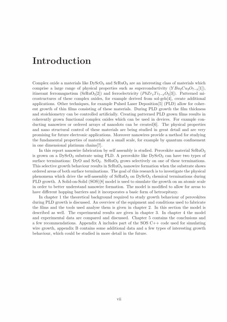
Height and phase TM-AFM images of three different samples which were annealed for 4hours as well, show mixed termination in two cases and possible single termination in one case.The images are depicted in figure 3.3. Sample (a) and (g) have a comparable stepwidth (130vs. 160 nm, while sample (d) has a large stepwidth (600 nm). Sample (a) and (d) show mixedtermination while sample (g) does not. Treatment of all samples was similar, except that sample(g) was cleaned and annealed separately from samples (a) and (d).
The height image of sample (a) shows almost perfectly flat terraces with unit cell 0.4 nmhigh steps, while a strong phase contrast is recorded simultaneously. The height image doesshow vague features centred on the terrace which correspond to the phase image. If any halfunit cell steps had to be appointed to these features it seems to be more likely to be 0.2 nm upinstead of the expected 0.2 nm down. Figure 3.1 (b) gives a schematic representation of a sucha 0.2 nm up, 0.4 nm up stacking and the corresponding friction pattern. This does not matchthe measured phase pattern and thus can not be the case. Stacking option (a) matches themeasured phase image, but does not match the 0.4 nm steps. Possibly the AFM friction forcesinfluence the height measurement and the real stacking is still option (c). Sample (d) clearlyshows that both the straightening of the step edges and the ordering of the mixed terminatedareas is not completed yet, due to the low miscut.
Substrates have also been annealed for 12, 16, 48 and 86 hours (not shown). For mostdifferent anneal times at least one mixed terminated substrate was found during this research.Many substrates did not show mixed termination, but seemed to be single terminated. Eventhough they had a similar miscut and were treated simultaneously.
3.2 PLD growth of SrRuO3 on DyScO3
SrRuO3 was grown by PLD using the experimental conditions described in section 2.2. Forevery sample RHEED images before growth, after growth and the intensity oscillations of thespecular spot were recorded. This section shows some typical examples of the RHEED signalbefore, during and after growth. Generally the evolution of the pattern shape was similar forall samples. The specular spot intensity oscillations did differ slightly. Images shown bellow areindicative of all grown films, nanowires, islands and smooth films.

3.2. PLD GROWTH OF SRRUO3 ON DYSCO3 19
(a) 30 min height (b) 30 min friction
0 200 400 600 8002
4
6
8
Hei
ght (
nm)
x (nm)0 200 400 600 800
50
100
150
200
Late
ral f
orce
(m
V)
(c) 30 min profile
(d) 4 hrs height (e) 4 hrs frictions
0 200 400 600 8000.5
1
1.5
2
2.5
3
3.5
Hei
ght (
nm)
x (nm)0 200 400 600 800
30
40
50
60
70
80
90
Late
ral f
orce
(m
V)
(f) 4 hrs profile
(g) 8 hrs height (h) 8 hrs frictions
0 200 400 600 800−2
0
2
Hei
ght (
nm)
x (nm)0 200 400 600 800
40
60
80
Late
ral f
orce
(m
V)
(i) 8 hrs profile
Figure: 3.2: Contact-AFM 1×1 µm height and friction images for various anneal times.Anneal process done at 1000 ◦C under oxygen flow. Height images (a,d)indicate 0.6 nm high steps preceded by 0.2nm steps near the centre of theterrace, resulting in an average height difference on one terrace of 0.4 nm.Part of the terraces show a different friction force (b,e) related to the 0.2 nmheight difference, these samples are mixed terminated. Images (g,h) showno clear mixed termination. Height and friction profiles (c,f,i) are averagedover 4 scan lines. The linescan position is indicated in the correspondingheight images.
3.2.1 RHEED before, during and after growth
Figure 3.4 (a),(c),(e) show images before growth for three different 2D crystal directions. Thedirections refer to a square representation of the surface. The direction are determined by therelative angles between successive RHEED patters during rotation of the sample. This leavesseveral options for the exact crystal direction. Assuming square symmetry these directionsare similar and are referred to by (10), (12) and (11). The angle between (10) and (12) is26.5◦and the angle between (12) and (11) is 18.5◦. The angles between (01)-(21) and (21)-(11)are 26.5◦and 18.5◦as well. Images (b),(d),(f) correspond to the same directions on the samesample after growth of SrRuO3. Before and after growth, all directions show a clear 2D RHEED
20 CHAPTER 3. EXPERIMENTAL RESULTS
(a) Height image (b) Phase image
0 0.5 1 1.5 20
1
2
3
4
Hei
ght (
nm)
x (µm)0 0.5 1 1.5 2
1
1.5
2
2.5
3
Pha
se (
degr
ees)
(c) Profiles
(d) Heigth image (e) Phase image
0 0.5 1 1.5 2 2.53
3.5
4
4.5
5
Hei
ght (
nm)
x (µm)0 0.5 1 1.5 2 2.5
2
4
6
8
10
Pha
se (
degr
ees)
(f) Profiles
(g) Heigth image (h) Phase image
0 0.5 1 1.5 20
1
2
3H
eigh
t (nm
)
x (µm)0 0.5 1 1.5 2
5
10
15
20
Pha
se (
degr
ees)
(i) Profiles
Figure: 3.3: TM-AFM (2×2 µm, 6×6 µm, 2×2 µm) height and phase images for varioussamples all annealed for 4 hours. Sample (a) and (g) had a similar mis-cut but only (a) shows mixed termination. Low miscut sample (d) showsclear mixed termination, but due to the low miscut the steps and mixedterminated areas are not straight. Profiles (c,f,i) are averaged over 4 scanlines.
pattern including Kikuchi lines[23]. However after growth more spots are visible, indicating a3D component to the surface morphology, normally related to island growth. These 3D spotsare relatively strong after growth in the (10)-direction.
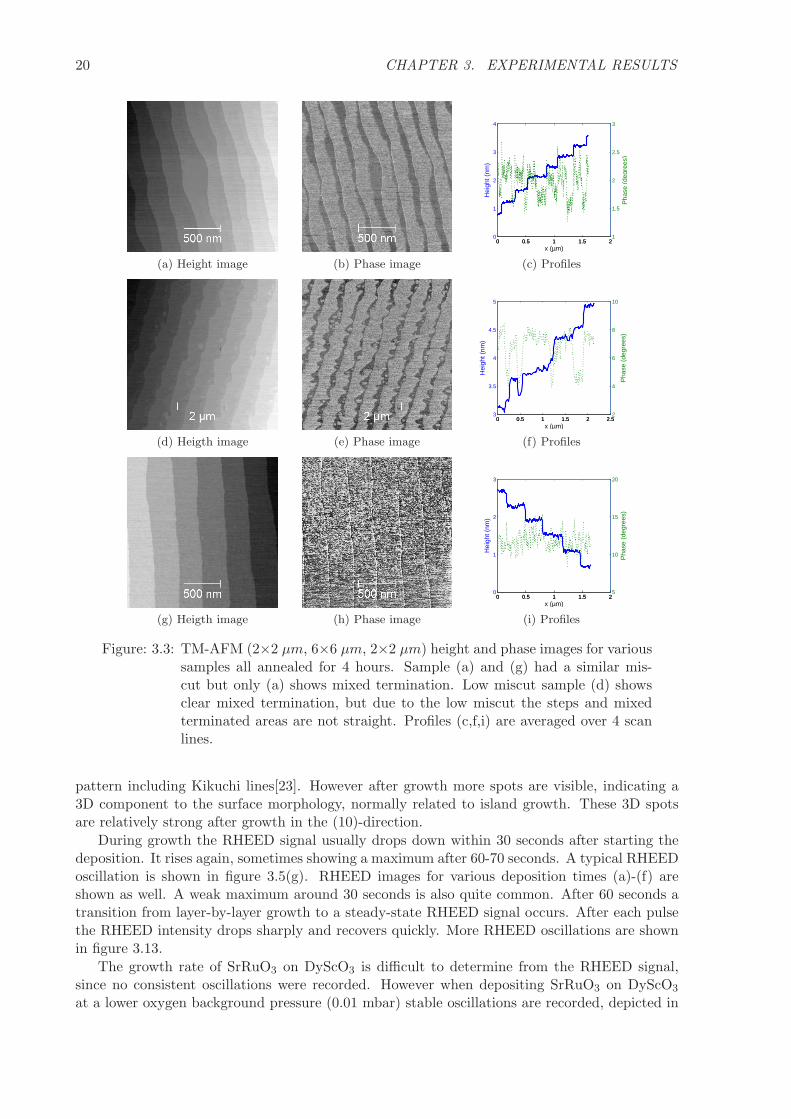
During growth the RHEED signal usually drops down within 30 seconds after starting thedeposition. It rises again, sometimes showing a maximum after 60-70 seconds. A typical RHEEDoscillation is shown in figure 3.5(g). RHEED images for various deposition times (a)-(f) areshown as well. A weak maximum around 30 seconds is also quite common. After 60 seconds atransition from layer-by-layer growth to a steady-state RHEED signal occurs. After each pulsethe RHEED intensity drops sharply and recovers quickly. More RHEED oscillations are shownin figure 3.13.
The growth rate of SrRuO3 on DyScO3 is difficult to determine from the RHEED signal,since no consistent oscillations were recorded. However when depositing SrRuO3 on DyScO3
at a lower oxygen background pressure (0.01 mbar) stable oscillations are recorded, depicted in

3.2. PLD GROWTH OF SRRUO3 ON DYSCO3 21
(a) before (11) (b) after (11)
(c) before (12) (d) after (12)
(e) before (10) (f) after (10)
Figure: 3.4: RHEED images before and after nanowire growth (SrRuO3 on DyScO3)for three different crystal directions. RHEED during growth for the samesample is depicted in figure 3.5. Images recorded at room temperature invacuum.
appendix B.3, figure B.4. These oscillations show 27 pulses are required for each monolayer ofSrRuO3. This roughly matches the first oscillation sometimes registered at higher pressure, 30seconds. For estimating the amount of SrRuO3 on DyScO3 during PLD 30 pulses per monolayerwill be used.
Surface morphology after growth
After growth on substrates shown in figure 3.2, STM image were recorded under vacuum con-ditions. The resulting STM images are depicted in figure 3.6. The SrRuO3 film morphologyclearly mimics the original substrate mixed termination. The lines are discussed in more detailin section 3.2.2. Figure 3.6(e) shows a relatively smooth film with only unit cell high steps. Theoriginal stepwidth is still visible as well. The top-left corner shows a measurement artefact.
3.2.2 Nanowire growth
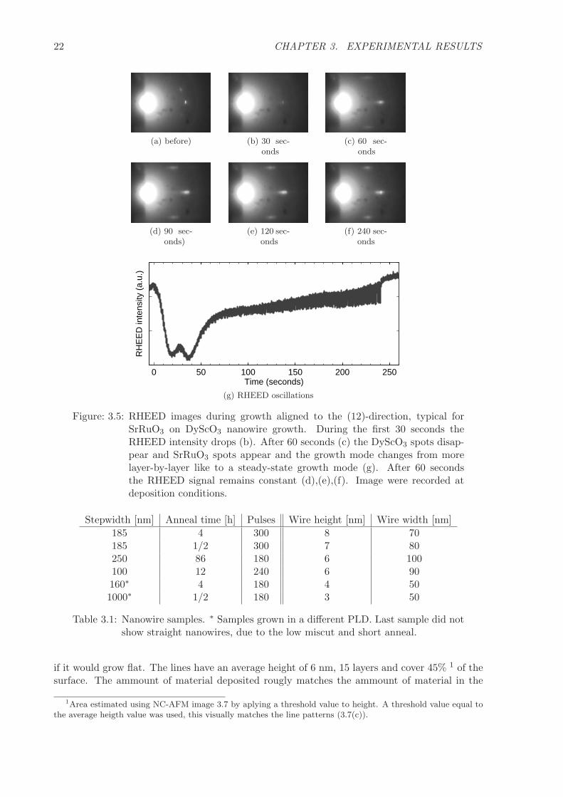
Table 3.1 gives an overview of the substrate and growth parameters which resulted in nanowiregrowth and the corresponding wire properties. The substrates which resulted in line patternedgrowth generally had a similar miscut. Lines were grown for three different deposition times, 3,4 and 5 minutes. The volume of the resulting wires scales with the deposition time. A maximumwire height of 8 nm was found.
The sample depicted in figure 3.7 shows nanowires after growth of 3 minutes, 180 pulses. Ata growth rate of 30 pulses per monolayer this corresponds to approximately 6 layers of SrRuO3
22 CHAPTER 3. EXPERIMENTAL RESULTS
(a) before) (b) 30 sec-onds
(c) 60 sec-onds
(d) 90 sec-onds)
(e) 120 sec-onds
(f) 240 sec-onds
0 50 100 150 200 250Time (seconds)
RH
EE
D in
tens
ity (
a.u.
)
(g) RHEED oscillations
Figure: 3.5: RHEED images during growth aligned to the (12)-direction, typical forSrRuO3 on DyScO3 nanowire growth. During the first 30 seconds theRHEED intensity drops (b). After 60 seconds (c) the DyScO3 spots disap-pear and SrRuO3 spots appear and the growth mode changes from morelayer-by-layer like to a steady-state growth mode (g). After 60 secondsthe RHEED signal remains constant (d),(e),(f). Image were recorded atdeposition conditions.
Stepwidth [nm] Anneal time [h] Pulses Wire height [nm] Wire width [nm]
185 4 300 8 70185 1/2 300 7 80250 86 180 6 100100 12 240 6 90160∗ 4 180 4 501000∗ 1/2 180 3 50
Table 3.1: Nanowire samples. ∗ Samples grown in a different PLD. Last sample did notshow straight nanowires, due to the low miscut and short anneal.
if it would grow flat. The lines have an average height of 6 nm, 15 layers and cover 45% 1 of thesurface. The ammount of material deposited rougly matches the ammount of material in the
1Area estimated using NC-AFM image 3.7 by aplying a threshold value to height. A threshold value equal tothe average heigth value was used, this visually matches the line patterns (3.7(c)).

3.2. PLD GROWTH OF SRRUO3 ON DYSCO3 23
(a) 30 min
0 0.5 12
4
6
8
10
12
x (µm)
heig
ht (
nm)
(b) 30 min profile
(c) 4 hrs
0 0.5 14
6
8
10
12
14
x (µm)he
ight
(nm
)
(d) 4 hrs profile
(e) 8 hrs
0 0.1 0.2 0.3 0.4
0.5
1
1.5
2
x (µm)
heig
ht (
nm)
(f) 8 hrs profile
Figure: 3.6: In-situ 1×1 µm STM images after 5 minutes of SrRuO3 growth for variousDyScO3 anneal times. Substrates correspond to AFM images depicted infigure 3.2. Line profiles (b,d,f) are averaged over 4 scan lines.
lines 45% × 15 = 6.75. This is very rough estimate, but it shows it is likely that no material isevaporated from the surface.
Figure 3.7d shows a height profile averaged over 4 scan lines. Original substrate stepwidthis clearly visible. The lines run directly next to or on top of the original step edge. Smallerlines are higher, thus the amount of material in one line remains constant. This also indicatesno material is evaporated from the surface during deposition.
Image 3.7b shows deep wells in the nanowires. The wells are as deep as the lines are high.These deep wells are expected to be related to defects the original mixed termination. This isnot confirmed. Occasionally and island grows in between the nanowires, four islands are visiblein image 3.7a. The islands have similar dimensions to the lines and the pair of islands in thelower left corner shows an island spacing comparable to the wire spacing. Indicating the wirespacing could be closely related to the diffusion length of SrRuO3 on DyScO3.

24 CHAPTER 3. EXPERIMENTAL RESULTS
(a) Lines (b) Lines zoom (c) Lines area
0 0.2 0.4 0.6 0.8 10
2
4
6
8
10
x (µm)
heig
ht (
nm)
1.2 nm
6.0 nm140 nm
125 nm
(d) Profile
Figure: 3.7: TM-AFM (5×5 µm, 1×1 µm, 5×5 µm) images of nanowires of SrRuO3
on DyScO3 after 3 minutes of SrRuO3 deposition. Image (a) and (b) showheight images and image (c) shows an overlay covering areas higher than theaverage height value of image (a). Image (d) shows a line profile averagedover 4 scan lines. The linescan corresponds to the line indicated in image(b). Typical nanowire properties are indicated as well(d). The originalsubstrates steps are still visible after nanowire growth.
3.2.3 Island growth
Instead of wires, some samples showed islands after growth. The height and width of these islandsare comparable to the height and width of line patterns. An overview of island properties forvarious samples is given in table 3.1 and two samples with islands are depicted in figure 3.8.
Stepwidth [nm] Anneal time [h] Pulses Island height [nm] Island size [nm] Coverage
222 4 360 8 50-90 70%170 1/2 240 4.5 30-100 56%282 15 240 5 30-80 52%
Table 3.2: Properties of samples with island. Islands are usually asymmetrically shapedand sizes distributed inhomogeneously.
The dimensions of the islands scales similar to the dimensions of wires, although their vari-ation in width is much larger. The inter-island distance is smaller and the coverage generallyslightly higher for islands compared to lines.

3.2. PLD GROWTH OF SRRUO3 ON DYSCO3 25
(a) Islands 4 min (b) Islands 6 min
Figure: 3.8: NC-AFM (1.5×1.5 µm, 2×2 µm) images islands after SrRuO3 growth of 4(a) and 6 (b) minutes indicating island growth.
3.2.4 Combined growth patterns
The nanowire sample discussed in the previous section already showed a few islands in betweenthe lines. While most of the time the growth ends up in either lines or islands, a combinedpattern is also possible, depicted in figure 3.9. Before deposition this sample showed areas withclear mixed termination, figure 3.9a and areas which showed almost no mixed termination, figure3.9c. The miscut direction and stepwidth varied locally on the substrate surface. This resultedin lines on certain areas (i) and islands (j) on other areas, but mainly a combination of both(e-h).
This combined growth mode could provide information about the mechanism responsiblefor growing wires. The lines are separated spatially stronger than the islands. Around wires adepletion zone is visible, indicating the lines act as sinks in an Oswald ripening process. Thelines grow at the expense of the smaller islands. However not all islands are influenced by thelines, only the islands closest to the lines. The distance the adatoms travel before nucleationcan be estimated using these images. The distance is related to the diffusion barrier used forsimulations. Figure 3.9e shows single islands between nanowires. The wire spacing is 240 nm,indicating a diffusion distance of 120 nm. Using an attempt frequency for hopping of 10 THzthis results in an activation energy of EA ≈ 1.3eV using equation 1.2. Rijnders [19] has foundan activation energy of 1.0 ± 0.2eV for SrRuO3 on SrTiO3.
3.2.5 Initial growth
To study the initial growth of SrRuO3 on DyScO3 mixed terminations, a short deposition wasperformed on a mixed terminated substrate. 30 Pulses were deposited using normal depositionconditions, table 2.1. Substrate CM-AFM images are depicted in figure 3.10a,b and TM-AFMimages of the film are shown in figure 3.10d,e. The height image and substrate profile 3.10cshow clear mixed termination before deposition. After growth the entire surface is coveredwith material and small islands grow everywhere. The height image and profile after growthshow regions of high islands and regions with lower islands. The ratio between these regions iscomparable to the mixed termination ratio of the substrate. The SrRuO3 film initially mimics thesubstrates mixed termination. Phase contrast is no longer visible after growth, this could indicatesingle termination after SrRuO3 growth. This seem likely when considering that Ru is highlyvolatile. Alternatively NC-AFM is less sensitive to SrRuO3 surface terminations compared toDyScO3 surface terminations.

26 CHAPTER 3. EXPERIMENTAL RESULTS
(a) Bef. height A (b) Bef. friction A
(c) Bef. height B (d) Be. friction B
(e) After (f) After (g) After
(h) After (i) After (j) After
Figure: 3.9: CM-AFM images before deposition (a-d) of SrRuO3 and NC-AFM imagesafter growth. All images are made on the same sample. (a,b,c,d,e,h) 3×3µm. (f,g) 2×2 µm. (i) 1.5×1.5 µm. (j) 2.4×2.4 µm.
3.3 DyScO3 termination control
Nanowire and island growth depends strongly on different growth behaviour of SrRuO3 on bothDyScO3 terminations. To test this different growth behaviour SrRuO3 was grown on DyScO3
with an additional layer of ScO2 and on DyScO3 with an additional layer of DyO.

3.3. DYSCO3 TERMINATION CONTROL 27
(a) height before (b) friction before
0 0.5 10.5
1
1.5
2
x (µm)
heig
ht (
nm)
0.2 nm
0.6 nm
(c) profile before
(d) height after (e) phase after
0 0.5 10
0.5
1
1.5
2
x (µm)
heig
ht (
nm)
(f) profile after
Figure: 3.10: CM-AFM 1×1 µm images of a mixed terminated DyScO3 substrate (a),(b)and TM-AFM images (d),(e) after growth of 30 pulses SrRuO3. Profiles(c),(f) are averaged over 4 scan lines.
3.3.1 SrRuO3 growth on ScO2
ScO2 was grown on DyScO3 from a Sc2O3 target using the parameters displayed in table 2.1.The growth rate of ScO2 was around 32 seconds per monolayer. An example RHEED oscillationis shown in figure B.1a. Exploratory experiments showed that for up to 3 layers of ScO2 theRHEED remained 2D. After the third layer 3D spots appeared. AFM images of a single ScO2
layer showed a smooth film, without any phase or friction contrast, depicted in appendix B, figureB.1a,b. Directly after growing a single layer of ScO2, 240 pulses of SrRuO3 were deposited atnormal SrRuO3 PLD parameters. The resulting NC-AFM images are shown in figure 3.11. Thefilm showed island growth. The phase image shows a contrast between the islands and lowerareas. The corresponding RHEED intensity oscillation is depicted in figure 3.13. The generalshape of this oscillation is common for SrRuO3 growth. The substrate used for growth of ScO2
followed by SrRuO3 had stepwidth of 170 nm.
(a) Height (b) Phase
Figure: 3.11: TM-AFM 1×1 µm images after SrRuO3 growth on ScO2 (a) height, (b)phase.

28 CHAPTER 3. EXPERIMENTAL RESULTS
3.3.2 SrRuO3 growth on DyO
Similarly to ScO2, DyO was grown on DyScO3 using the parameters displayed in table 2.1 froma Dy2O3 target. To growth rate is approximately 30 pulses per monolayer. After growth of 2layers of DyO the RHEED pattern completely disappears indicating no single crystal or epitaxialfilm was grown. Likely caused by the large lattice mismatch between Dy2O3 and DyScO3. Aftergrowth of a single monolayer of DyO, NC-AFM images still indicated a smooth film, almostsimilar to the DyScO3 substrate, depicted in appendix B figure B.2a,b. A RHEED intensityexample for DyO growth is depicted in figure B.2e.
(a) Height (b) Phase
(c) Autocorr. (d) Zoom
Figure: 3.12: TM-AFM images after SrRuO3 growth on DyOImage (a) shows a heightimage, (b) a phase image. Image (d) shows a zoom of the height image.An auto correlation map is plotted in figure (c), indicating ordered islands.(a-c) 6×6 µm, (d) 0.5×0.5 µm.
240 pulses of SrRuO3 were added to this layer of DyO on a substrate with a stepwidthof 200 nm. The RHEED intensity oscillation is shown in figure 3.13. The general shape ofthis oscillation is common for SrRuO3 growth. However the time-scale differs slightly from thegrowth of SrRuO3 on ScO2. When comparing the RHEED oscillation for growth of SrRuO3 onDyO or ScO2 in figure 3.5g: ScO2 matches normal SrRuO3 growth closest. NC-AFM imagesof the SrRuO3 film on DyO show islands, depicted in figure 3.12a,b,d. The islands are clearlyelongated in one direction. Phase image (b) shows a contrast between the islands and lowerareas, indicating the lower areas are likely to be a different material or termination. An auto-correlation function of the height image is shown in figure 3.12c. This auto-correlation functionshows a striped pattern. The stripes are separated roughly by 200 nm, the original substratestepwidth.

3.4. SRRUO3 FILM PROPERTIES 29
0 50 100 150 200 250 300
Time (seconds)
Inte
nsity
(a.
u.)
SRO on DyO (upper line) SRO on ScO (lower line)SRO on DSO
67 sec
28 sec 82 sec
Figure: 3.13: RHEED intensity oscillations for SrRuO3 growth on DyScO3 with eitherone layer of DyO (black), ScO2 (light grey) sandwiched between bothlayers. For comparison also a normal oscillation is shown. (grey)
3.4 SrRuO3 film properties
3.4.1 SEM imaging & electrical measurements
Scanning Electron Microscope (SEM) image of a sample depicted were recorded, depicted infigure 3.7. Two zoom levels of this sample are depicted in figure 3.14(a)(b). Image 3.14a showslong-range ordered nanowires up to at least 25 µm. Nanoprobe IV curves were recorded2. The IVcurves do not give any quantitative information. Figure 3.14e shows a voltage response which islikely due to contact resistance. Both the current running trough the upper and lower probe tipwere recorded and are plotted on different axis. Figure 3.14f shows no voltage response. Mind thedifferent range between figures (e) and (f). In figure 3.14c wires light in the SEM image up duringthe voltage measurements. This indicates current is flowing through the lines which is registeredby the SEM. Such effects were not registered when the probes were positioned perpendicularto the nanowire direction. Several attempts to measure electrical properties by contacting thesurface via gold contacts failed. Either the films were insulating or the measurements failed.
3.4.2 Conductivity mapping
At Stanford, Microwave impedance microscopy scans were made on a nanowire sample. Theresults are depicted in figure 3.15. The MIM images shows a strong contrast related to thenanowires. The MIM tip dimensions matched the nanowire spacing. The tip probably did notreach the bottom of the valleys between the nanowires resulting in resulting in a non uniformMIM-C signal around the nanowires.
3.4.3 X-Ray spectroscopy
XPS data of several films were recorded. Spectra of the Ru 3d band provide more informationabout electron correlation in the SrRuO3 film[24]. The appearance of an additional screenedpeak indicates the transition from insulating to metallic films. This is not studied in this report.Example XPS data are included in appendix B.3.
3.5 Model results
A selection of simulations results is depicted and interpreted in this section. All simulationswere done using the nanowire simulation parameters in table 2.2, variations in parameters areexplicitly mentioned.
2Measurements performed by Peter de Veen.

30 CHAPTER 3. EXPERIMENTAL RESULTS
(a) 5000X (b) 35000X
(c) Par. to lines (d) Perp. to lines
0 2 4 6 8 100
50
100
150
200
AI (
pA)
Applied Voltage (V)0 2 4 6 8 10
−200
−150
−100
−50
0
BI (
pA)
(e) IV curve par.
0 2 4 6 8 10−1
−0.5
0
0.5
1
1.5
2
AI (
pA)
Applied Voltage (V)0 2 4 6 8 10
−1
−0.5
0
0.5
1
1.5
2
BI (
pA)
(f) IV curve perp.
Figure: 3.14: SEM images of SrRuO3 nanowires indicating long-range order (a),(b) andIV curves (e),(f) recorded for directions parallel the lines (c) and per-pendicular to the lines (d). During voltage sweep the nanowires light up(c) indicating a response to the measurement. No transport is measuredperpendicular to the nanowires. Dark square areas image (d) caused bycontaminations due to scanning areas with the SEM.
3.5.1 Nanowire growth
Two nanowire surface morphology evolutions are depicted in figure 3.16 for different valuesof EB. Parameters used for this nanowire simulation were: EA
S = 0.55 eV ; EBS = 0.85 eV ;
ES = 0.75 eV ; EN = 0.25 eV ; T = 573 K and stepwidth = 68 nm. Figure 3.16a shows twodifferent regions of surface diffusion barrier ES , dark areas indicate a low ES value, a highdiffusivity. Morphology evolutions (left) and (right) indicate wire growth for EB = 0.01 eV/celland EB = 0.025 eV/cell respectively.
The first layer grows step-flow on A-site areas, no islands grow on the A-site area. The

3.5. MODEL RESULTS 31
(a) Height A (b) MIM-C A
(c) Height B (d) MIM-C B
Figure: 3.15: AFM (a),(c) and MIM-C (b)(d) images on two nanowire samples. SampleA also depicted in figure 3.6c. Both images show a MIM contrast relatedto the nanowires
materials reaches the B-site areas by step-flow across the A-site areas and sticks as soon asit reaches a B-site area. This is visible around near the boundaries of the B-site areas, mostmaterial initially sticks at the B-site boundary. Material arrives on both sides of the B-siteterminated areas. For the first layer, EB does not yet play a role. After completion of the firstlayer of material on the B-site area, the value of ES changes from EB
S = 0.85 to ES = 0.75.This enhanced diffusion is indicated by larger islands on top of the first layer of the nanowire,compare image row 1 with row 5 for example, but it does not play any major role. If no EB
value is used, EB = 0, the wires will continue to grow, exactly matching the original mixedtermination (not shown). It is not realistic to allow adatoms to jump up high wires or islandsin one single step, so an Eadd barrier is added. Such a barrier for two different EB values asdiscussed in section 2.4.2. A higher EB value results in wider and lower nanowires. ChangingEB with respect to the stepwidth and mixed termination ratio provides a method to tune thesimulated wire properties to match experimental data.
3.5.2 Island and smooth growth
The nanowires simulations were also run without substrate mixed termination on both singleA-site and single B-site termination. The results are depicted in figure 3.17, (left) A-site termi-nation, (right) B-site termination. Simulation was run with the same parameters as for nanowiregrowth depicted in figure 3.16(left). On the A-site, high diffusivity termination high islands ofSrRuO3 grow. The first layer of small SrRuO3 islands act as sink sites for newly arriving SrRuO3
cells, similar to B-site termination and larger islands form on the surface. The SrRuO3 islandprevent step-flow growth mode. In case of B-site termination the difference between substrateand SrRuO3 is much smaller and normal layer-by-layer growth occurs. This smooth growth ismeasured during PLD as well[11] when the substrates are chemically treated.
3.5.3 Combined growth
On substrates with a lower miscut, a combined island and wire growth mode was simulatedusing the SOS model. Parameters used were the same as for nanowire sample 3.16(left), onlythe stepwidth was increased to 102 nm. These results match experimental observations of islandsgrowing in between the nanowires. Low miscut results are depicted in figure 3.18.

32 CHAPTER 3. EXPERIMENTAL RESULTS
(a) Mixed termination
(t) EB = 0.01 eV/cell (u) EB = 0.025 eV/cell
Figure: 3.16: Nanowire SOS simulation results for two different EB values. Image (a)indicates to the original substrate ES values, dark areas correspond to alow ES value, high diffusivity, A-site termination. Left series done usingEB = 0.01 eV/cell, right series using EB = 0.025 eV/cell. The seriesshow a different evolution of the nanowires width and height. Images fromtop to bottom correspond to deposition of 1,15,30,45,60,75,90,105,120,135pulses.

3.5. MODEL RESULTS 33
(u) A-site (v) B-site
Figure: 3.17: Simulation results for single terminated A-site and B-site substrates, EB =0.01 eV . Indicating island growth on A-site termination and a smooth filmis grown on B-site termination. Images from top to bottom correspond todeposition of 1,15,30,45,60,75,90,105,120,135,150 pulses.

34 CHAPTER 3. EXPERIMENTAL RESULTS
(a) Mixed termination
Figure: 3.18: SOS simulation on a sample with a stepwidth of 102 nm and EB = 0.01 eV .Image (a) indicates to the original substrate ES values, dark areas corre-spond to a low ES value, high diffusivity, A-site termination. Islandsgrow on the A-site terrace wile a nanowire grows on the B-site ter-race. Images from top-left to bottom-right correspond to deposition of1,15,30,45,60,75,90,105,120,135,150,165 pulses.

Chapter 4
Discussion: model versus
experiments
In this chapter the experimental data will be discussed, mainly in relationship with the simula-tion results. First DyScO3 substrate influences are discussed. Secondly the proposed physicalmechanism governing wire growth is discussed by comparing PLD grown films and simulations.Finally the validity of the model is discussed.
4.1 The DyScO3 surface
Annealed DyScO3 substrates show ordered areas of both DyO and ScO2 surface terminations.After sufficiently long annealing the mixed terminated regions line up along a step edge. Theminimum anneal time required to acquire line shaped areas of mixed termination is equal tothe time required to create straight step edges. AFM friction or phase images show a contrastrelated to the surface termination usually accompanied by a height contrast. Figure 3.1c showsthe the stacking of mixed terminated areas deduced from AFM height images. On a mixedterminated substrate each terrace consists of a 0.6 nm (1.5 u.c.) step up and a 0.2 nm (0.5u.c.) step down. No clear relation between anneal time and the amount of mixed termina-tion was found. Preliminary anneal experiments indicated mixed termination disappeared afterlong annealing, however two 86 hours annealed substrates still showed clear mixed termination.Moreover mixed termination was detected for substrates annealed for various anneal times. Thesurface stoichiometry seems to change continuously during annealing. The exact ratio betweenDyO and ScO2 at the surface is expected to depend on the mixed termination ratio prior toannealing combined with the substrates terrace width and the anneal time.
4.2 SrRuO3 nanowire growth
AFM and RHEED data show that during PLD growth SrRuO3 mimics the DyScO3 substratemixed termination areas. SrRuO3 nucleates preferentially on one surface termination. Nomaterial is evaporated during growth, as the height of the wires scales with the mixed terminationratio. In other words the volume of the nanowires is equal to volume expected from the RHEEDsignal. Material deposited between the lines diffuses until it nucleates on a nanowire. Thenanowires grow in height and width simultaneously. This kinetic balance is studied successfullyusing a SOS model. The SOS models assumes difference of ∆ES = 0.3 eV between both diffusionbarriers. Compared to the nearest neighbour bond energy of EN = 0.25 eV it is preferential tohop onto the areas with the highest ES value, even if this hop crosses a step in the substrate.Next to this difference in diffusion barriers the diffusion length of adatoms on A-site areas must
35

36 CHAPTER 4. DISCUSSION: MODEL VERSUS EXPERIMENTS
be larger than the step width in order to grow nanowires. Otherwise islands grow in betweenthe nanowires, similar to PLD grown nanowires.
Preferred termination
The model requires a difference in diffusivity for both surface terminations. The terminationwhich has the lowest diffusivity will act as a sink site for adatoms to nucleate, this is thepreferred termination for nanowire growth. SrRuO3 also grows selectively on SrTiO3 mixedterminations [25], where it is assumed to grow on TiO2 termination. This is supported bySrRuO3 growth on chemically treated SrTiO3 substrate [10] resulting in TiO2 termination. Ifnot all SrO is chemically etched, deep trenches remain present after growth of SrRuO3, relatedto the SrO terminated areas. If growth on TiO2 is driven by selective growth of SrRuO3 onB-site terminated crystals, the same preference is expected for growth on DyScO3.
Termination conversion & initial growth
Using similar SrRuO3 PLD parameters on SrTiO3 substrates, a termination conversion in regis-tered in the RHEED signal, described in section 1.3.2. This same conversion is measured whengrowing on DyScO3, indicating a large area of the surface is ScO2 terminated and the nanowiresgrow on this termination. Sometimes a weak oscillation is recorded with a maximum after 30seconds, for example depicted in figure 3.5g. This maximum could be related to the degree ofmixed termination. The A-site area of the substrate would be growing 1 full mono-layer in 30seconds while the remaining B-site area would require more time to switch termination beforecompleting the first mono-layer. This does not provide conclusive evidence about the preferredtermination, since this extra oscillation did not show systematically. The model assumes nomaterial grows on A-site termination, so this explanation does not match the model. Two morephenomena can explain the 30 seconds maximum. In the first place, if SrRuO3 only grows onScO2 which covers 50% of the surface and no material evaporates: the number of pulses requiredto create a smooth layer is expected to be half the number of pulses required for 100% ScO2
termination. This decreased first oscillation length was not registered systematically. Howeverthis change in oscillation period does give an explantion for the irregular lenght of the mea-sured first oscillation, for example between SrRuO3 growth on deposited ScO2 and DyO thisfirst oscillation differed by 15 seconds, figure 3.13. Secondly, during termination conversion anintermediate smooth layer could form, not as smooth as a for full oscillation, but still show upin the RHEED signal. The exact origin of the 30 seconds maximum remains unknown.
AFM images made after growth of 30 seconds of deposition, figure 3.10, shows material clearlygrows more quickly on one termination, even before a termination conversion has occurred.These possible stacking variations are depicted schematically in figure 4.1 assuming substratestacking 3.1c. Initial growth shows 0.8-1.2 nm heigh steps after 30 seconds of deposition. Onlyoption (d) is able to explain these high features after 30 seconds. The termination on top of the0.6 nm step is expected to be the preferred termination. The double period of the first RHEEDoscillation indicates this termination is ScO2.
Controlled surface termination analysis
Deposition of ScO2 and DyO layers on a DyScO3 substrate before SrRuO3 film growth results indifferent RHEED signals. These RHEED intensity oscillations during growth of SrRuO3 on topof these single oxide layers are depicted in figure 3.13. Both show a long first layer completiontime. Likely not the entire surface was covered with DyO after Dy2O3 deposition, leaving theremaining ScO2 to act as sink sites for the anisotropic growth depicted in figure 3.12. The growthof SrRuO3 on ScO2 terminated DyScO3 by deposition of Sc2O3 resulted in island growth. This

4.3. PHYSICAL MECHANISM 37
(a) (b) (c) (d)
B-site: ScO2
A-site: DyO
B-site: RuO2
A-site: SrO
Figure: 4.1: Possible detailed stacking options after growth of SrRuO3 on mixed termi-nated DyScO3 after 60 seconds of deposition, assuming substrate stackingoption 3.1c. If no selective growth occurs and termination conversion takesplace on the lowest terrace areas (a) or on the highest terrace areas (b)and assuming selective growth of SrRuO3 on ScO2 terminated areas: onthe lowest terrace areas (c) or on the highest terrace areas (d).
does not match the idea that nanowires grow coherently on ScO2 termination. Coherent growthis expected for single termination after chemical treatment, most likely ScO2[11]. Possibly thedeposition of a single ScO2 layer from the Sc2O3 target failed.
Comparison with other types of anomalous growth
Wire patterned growth of SrRuO3 on LaAlO3 is explained by a stress relaxation due to therelatively high lattice mismatch between SrRuO3 and LaAlO3[26]. Rippled patterned islandform on the substrate. Island grow on the ripples while inter ripple regions remain uncovered.After growth of 5 nm these island coalesce to form rippled wire structures. This mechanism isvery different from the model proposed in this report, it does not involve mixed termination.The wires resulting from SrRuO3 growth on LaAlO3 are not as well defined as SrRuO3 wires onDyScO3. The wire spacing is small and the height varied greatly.
SrRuO3 wired patterns were grown on SrTiO3 surface terminations[25], similar to DyScO3
surface terminations. The growth of these wires is attributed to a difference in adatom stickingcoefficient. The resulting wires are almost as wide as the original terraces, separated by smalltrenches. These SrRuO3 wires do not show the same long range spatial order and separationas SrRuO3 wires on DyScO3. Other types of anisotropic growth for metals instead of complexoxides originate from preferred nucleation at step edges[27, 7] or form by self-organized growthon strain-relief patterns caused by dislocations[28]. These mechanisms do not involve mixedsurface terminations.
4.3 Physical mechanism
The SOS model explained in section 2.4.3 matches the results in chapter 3 qualitatively. A mixedterminated substrate results in nanowires assuming DyO termination to have a high diffusivitycompared to ScO2 termination ans SrRuO3 covered areas, figure 3.16. Nanowire formation is aresult of mixed terminated areas which have a different diffusivity. By incorporating a step-upbarrier related to the height of the wires the evolution of the wires width and height matchesthe measured evolution. The wires grow in width and height simultaneously in both the modeland the experiments. The model shows that as the wires grow in height the chance of new cells

38 CHAPTER 4. DISCUSSION: MODEL VERSUS EXPERIMENTS
reaching the top of the wire decreases and the wires start growing in width more quickly. Islandsoccasionally grow in between the nanowires. This island growth is simulated by increasing thestepwidth while keeping the other SOS parameters constant. The diffusion length lD of theSrRuO3 cells on DyO termination becomes smaller than the nanowire spacing. This resulting inSrRuO3 island in between the lines. Since the diffusion coefficient of SrRuO3 on these SrRuO3
island is also low compared to SrRuO3 on DyO, these islands grow in height similar to the mixedterminated ScO2 areas.
This diffusion length limit does not explain the combined growth patters measured on asubstrate which showed a large local variation in miscut angle and stepwidth, figure 3.9. Thissample’s wires and islands give rise to an an alternative explanation for island growth. Islandgrowth could also be caused by areas of ScO2 which remain on the substrate after annealing.Annealing is a diffusion driven process, just like PLD growth. Islands of ScO2 are most likelyto be found on the centres of step terraces if they did not reach a step edge during annealing.However these island were never recorded except for this one sample which showed many features.If the annealed substrates do not show friction or phase contrast on the terraces, the islands inbetween nanowires are expected to be caused by diffusion during SrRuO3 growth and not byislands of ScO2 termination.
If single terminated substrates are simulated using the same parameters, the results alsoshow a qualitative match with the measurements. A simulation of DyO termination results inisland growth similar to some PLD results. The model thus implies island growth occurs onsubstrates which do not have ScO2 sinks. Simulation on ScO2 termination result in smoothfilms. According to the SOS model chemically treated single terminated substrates[11] resultingin smooth SrRuO3 films after PLD growth are ScO2 single terminated.
4.4 Model validity
The model nanowires are in good qualitative agreement with the PLD grown nanowires. Themodel requires a difference in the substrate diffusion barrier of 0.3 eV (section 2.4.3). This 0.3eV difference is large enough to change step-flow growth into layer-by-layer growth (2.4.1). Sucha transition is measured for growth of SrRuO3 on SrTiO3 after completion of the first layer[14].The SOS ES parameter varied from 0.75 eV to 1.3 eV for various applications[19, 20, 22] and EN
varied between 0.25 eV and 0.65 eV. The chosen parameters are within this range. Except forthe substrate diffusion barrier on DyO, this EB
S was chosen slightly lower to enhance diffusivity.The chosen parameters are mostly within established ranges. In order to get a quantitativematch, the model should be used at higher temperatures and for lower miscut samples. Thislower miscut requires simulation of larger areas. These large areas combined with the highertemperatures increase simulation time drastically.
Step up barrier
Basic SOS models[8] do not allow atoms to hop onto steps or islands, either by explicitly pro-hibiting this hop or because it is energetically unfavourable. It is not realistic to allow atoms tohop directly onto multiple unit cell high nanowires. The modified SOS models corrects for thisby adding an additional barrier for cells hopping onto a nanowire. The barrier scales with theheight difference an adatom must overcome to hop onto a higher area. Without this barrier thesimulation only provides information on the initial growth of the first few layers. The barrierwas tuned to acquire a qualitative match between simulation and measurements.

Chapter 5
Conclusions & Recommendations
The surface mixed termination ratio of DyScO3(110) substrates can be tuned by annealingfor different periods of time. The exact mixed termination ratio depends on the anneal time,substrates miscut angle and an unknown additional factor, possibly the post-anneal mixed termi-nation ratio. During annealing the surface stoichiometry changes continuously, it is not possibleto achieve single termination by long annealing. The best method for acquiring mixed termina-tion suitable for nanowire growth is to anneal at least 2 hours at 1000 ◦C to straighten the stepedges on pre-selected vicinal substrates, miscut angle ≈ 0.1◦. Annealing for 4 hours resulted inthe highest number of ordered mixed terminated substrates.
AFM analyses after growth indicates SrRuO3 mimics the original DyScO3(110) chemicalterminations during PLD. According the the measured termination conversion RHEED signal,the nanowires grow selectively on ScO2 termination. Typical nanowires show a height of 6 nm,width of 80 nm and are separated by 100 nm. When the nanowire spacing is increased, islandsgrow in between the wires. Growth on substrates which did not show mixed termination usuallyresulted in island growth.
The SrRuO3 nanowires, islands and smooth films were simulated using a Solid-on-Solidmodel by assuming high diffusivity on DyO terminated areas compared to both ScO2 terminatedareas and the SrRuO3 covered areas. By adding an additional hopping barrier which increaseslinearly with the nanowire or island height, the wire width and height evolution during growthwas simulated successfully. The same model was adopted to explain island growth on DyO singleterminated films and smooth film growth on ScO2 single terminated substrates. By changingsubstrate stepwidth or the additional hopping barrier, the height and width evolution duringsimulations can be modified. Simulation resulting in nanowire growth were performed with asurface diffusion barrier of 0.55 eV on DyO terminated areas, 0.85 eV on ScO2 terminated areasand a nearest-neighbour bond energy of 0.25 eV. The additional hopping barrier matched theexperimental data when chosen around 0.01 eV per unit cell high step.
SrRuO3 conducting nanowires physical properties show a clear contrast with respect to theinsulating DyScO3 substrates using MIM. The nanowires show an anisotropic responds to two-point electrical measurements when the probes are aligned either parallel or perpendicular withrespect to the nanowires.
Recommendations
The DyScO3 substrate mixed termination is currently acquired by a method which does notguarantee mixed termination. More control on the mixed termination ratio provides more controlover the nanowire dimensions and quality. During the final stages of this master’s thesis a methodfor acquiring single terminated substrates was developed[11]. These single terminated substratescould be used as a starting point for creating mixed terminated substrates with a controllable
39

40 CHAPTER 5. CONCLUSIONS & RECOMMENDATIONS
amount of both chemical terminations. For example by annealing single terminated substratesfor various periods of time. More knowledge about the DyScO3 substrate will most likely leadto even more well defined nanowires.
The current simulation parameters are based on previously performed SrRuO3 hetroepitaxymeasurements and MBE simulations. A large difference between DyO and ScO2 surface dif-fusivity is assumed in the SOS model. Actual measurements of the diffusivity of SrRuO3 onboth terminations will provide quantitative information on the diffusivity difference. For in-stance by measuring the RHEED recovery time as a function of temperature. This requires alarge dataset and requires to be able to precisely control the surface termination. This could bedone by studying single oxide, Sc2O3, Dy2O3 deposition in more detail and/or use of chemicaltreatment.
Only initial transport measurements were attempted during this research which indicatedSrRuO3 nanowire properties differ from bulk properties, SrRuO3 nanowires seem to have ahigher resistivity compared to bulk SrRuO3. The physical properties of the nanowires areof high interest for their possible applications. These properties should be determined moreprecisely. SrRuO3 shows a metal insulator transition on SrTiO3 substrates as a function of filmthickness[2]. This transition is expected to be different on DyScO3 substrates due to the tensileinstead of compressive strain on DyScO3 with respect to SrTiO3. This transition might occurin the nanowires as well and could provide more information about the mechanism behind thetransition. Initial XPS data depicted in appendix B.3 indicate the SrRuO3 nanowires differ fromthick SrRuO3 films on DyScO3 with respect to their transport properties. Conductive AFM onthe nanowires could provide more information about the electrical properties as well.
PLD growth parameters were mostly kept constant during this research. Variations resultedin interesting growth behaviour depicted in appendix B.3. Changes in PLD conditions could beused to control nanowire dimensions.
SrRuO3 is sensitive to different surface terminations during growth, possibly due to it’s highdiffusivity or the highly volatile Ru species. It is interesting to study why SrRuO3 is sensitiveto mixed termination and why this termination difference gives rise to a difference in diffusivity.There might also be other materials that show selective growth behaviour and have differentfunctional properties. Possibly several materials can be combined to grow structured films withembedded patterns.

Dankwoord
Zes jaar, een maand en negen dagen studeren komen samen in een verslag en een presentatie.Het studentenleven is voorbij, sneller dan je zou verwachten als je er midden in zit. Ik wil graageen aantal mensen bedanken die deze tijd ontzettend leuk en gezellig hebben gemaakt.
Dat zijn allereerst mijn ouders die mij zowel moreel als financieel gesteund hebben. Helaasheeft mijn vader mijn afstuderen niet mogen meemaken. Natuurlijk ook dank aan mijn lievevriendin Marloes voor de gezellige tijd naast het studeren en de enorme morele steun. Ook mijngrootste fan en broertje Rens bedankt voor het veroorzaken van meer afleiding dan hij zelf be-doelt. Natuurlijk ook dank aan alle vrienden voor de nodige afleiding en plezier: studiegenoten,huisgenoten en DIOK’ers. Zowel op de badminton baan als daarnaast.
De vakgroep Inorganic Materials Science bedankt! In de studentenkamer was altijd wel ietste beleven. De gezelligste vakgroep van TNW wat mij betreft. Mijn dagelijks begeleider JeroenBlok heeft mij altijd scherp gehouden en hij heeft mij samen met Gert Jan Koster ruimschootsvoorzien in de wetenschappelijke feedback en input voor mijn onderzoek, waarvoor veel dank.Harold Zandvliet wil ik bedanken voor de nuttige discussies over het ontstaan van de draden.Daarnaast heb ik in het lab veel lol gehad met het hele COMAT team, Hans, Josee, Joost,Andreas en Jeroen, waarvoor eveneens dank.
Bouwe Kuiper - oktober 2009
41


References
[1] J.G. Bednorz and K. A. Muller. Possible high Tc superconductivity in the Ba-La-Cu-Osystem. Zeitschrift fur Physik B Condensed Matter, 64:189–193, 1986.
[2] Jing Xia, W. Siemons, G. Koster, M. R. Beasley, and A. Kapitulnik. Critical thicknessfor itinerant ferromagnetism in ultrathin films of srruo3. Physical Review B (CondensedMatter and Materials Physics), 79(14):140407, 2009.
[3] M. Dawber, K.M. Rabe, and J.F. Scott. Physics of thin-film ferroelectric oxides. Reviewsof Modern Physics, 77:1083–1130, October 2005.
[4] S Seraji, Y Wu, NE Jewell-Larson, MJ Forbess, SJ Limmer, TP Chou, and GZ Cao.Patterned microstructure of sol-gel derived complex oxides using soft lithography. AdvancedMaterials, 12(19):1421–1424, OCT 2 2000.
[5] Dave H. A. Blank, Guus J. H. M. Rijnders, Gertjan Koster, and Horst Rogalla. In-situmonitoring during pulsed laser deposition using rheed at high pressure. Applied SurfaceScience, 127-129:633 – 638, 1998. ISSN 0169-4332.
[6] Paul Marie Riele te. Direct patterning of oxides by pulsed laser stencil deposition. PhDthesis, Enschede, September 2008.
[7] Nuri Oncel, Arie Houselt van, Jeroen Huijben, Ann-Sofie Hallback, Oguzhan Gurlu,Harold J.W. Zandvliet, and Bene Poelsema. Quantum confinement between self-organizedpt nanowires on ge(001). Physical Review Letters, 95(11):116801–1, 2005.
[8] K. Malarz and A.Z. Maksymowicz. A simple solid-on-solid model of epitaxial thin filmsgrowth: surface morphology anisotropy. Int. Journal of Modern Physics C, 10:659, 1999.
[9] M. D. Biegalski, J. H. Haeni, S. Trolier-McKinstry, D. G. Schlom, C. D. Brandle, andA. J. V. Graitis. Thermal expansion of the new perovskite substrates DyScO3 and GdScO3.Journal of Materials Research, 20:952–958, 2005.
[10] Gertjan Koster, Boike L. Kropman, Guus J. H. M. Rijnders, Dave H. A. Blank, and HorstRogalla. Quasi-ideal strontium titanate crystal surfaces through formation of strontiumhydroxide. Applied Physics Letters, 73(20):2920–2922, 1998.
[11] J.E. Kleibeuker and D. Dubbink. Unpublised. Unknown journal; Bachelor’s thesis, 2009.
[12] Ivan V Markov. Crystal growth for beginners: Fundamentals of Nucleation, Crystal Growthand Epitaxy. World Scientific, 1995.
[13] J.J. Broekmaat. In-situ growth monitoring with scanning force microscopy during pulsedlaser deposition. PhD thesis, Enschede, April 2008.
[14] Guus Rijnders, Dave H. A. Blank, Junghoon Choi, and Chang-Beom Eom. Enhancedsurface diffusion through termination conversion during epitaxial srruo growth. AppliedPhysics Letters, 84(4):505–507, 2004.
[15] John D. Weeks and George H. Gilmer. Dynamics of crystal growth. Advances in ChemicalPhysics, 99(1-4):157–228, 1979.
[16] P A Maksym. Fast monte carlo simulation of mbe growth. Semiconductor Science andTechnology, 3(6):594–596, 1988.
43

44 REFERENCES
[17] A. Lopez, T. Heller, T. Bitzer, Q. Chen, and N. V. Richardson. The influence of sodium onthe adsorption of water on srtio3(100)-1x1 surfaces. Surface Science, 494(3):L811 – L814,2001. ISSN 0039-6028.
[18] K. Lai, W. Kundhikanjana, H. Peng, Y. Cui, M. A. Kelly, and Z. X. Shen. Tapping modemicrowave impedance microscopy. Review of Scientific Instruments, 80(4):043707–+, April2009.
[19] A.J.H.M. Rijnders. The initial growth of complex oxides : study and manipulation. PhDthesis, Enschede, October 2001.
[20] T. Kawamura and T. Natori. Extended solid-on-solid model for heteroepitaxial growth.Surface Science, 438(1-3):148 – 154, 1999. ISSN 0039-6028.
[21] M. H. Xie, S. Y. Leung, and S. Y. Tong. What causes step bunching–negative ehrlich-schwoebel barrier versus positive incorporation barrier. Surface Science, 515(1):L459 –L463, 2002. ISSN 0039-6028.
[22] D. D. Vvedensky, S. Clarke, K. J. Hugill, M. R. Wilby, and T. Kawamura. Growth kineticson vicinal surfaces. Journal of Crystal Growth, 99(1-4):54 – 59, 1990. ISSN 0022-0248.
[23] Wolfgang Braun. Applied RHEED: Reflection High-Energy Electron Diffraction duringcrystal growth. Springer, 1999.
[24] Hyeong-Do Kim, Han-Jin Noh, K.H. Kim, and S.-J. Oh. Core-level photoemission revealingthe mott transition. Physica B: Condensed Matter, 359-361:1267 – 1269, 2005. ISSN 0921-4526. Proceedings of the International Conference on Strongly Correlated Electron Systems.
[25] R. Bachelet, F. Sanchez, J. Santiso, C. Munuera, C. Ocal, and J. Fontcuberta. Self-Assemblyof SrTiO3(001) Chemical-Terminations: A Route for Oxide-Nanostructure Fabrication bySelective Growth. Chemistry of materials, 21(12):2494–2498, JUN 23 2009.
[26] E. Vasco, R. Dittmann, S. Karthauser, and R. Waser. Early self-assembled stages in epi-taxial srruo on laalo. Applied Physics Letters, 82(15):2497–2499, 2003.
[27] P. Gambardella, M. Blanc, H. Brune, K. Kuhnke, and K. Kern. One-dimensional metalchains on pt vicinal surfaces. Phys. Rev. B, 61(3):2254–2262, Jan 2000.
[28] H Brune, M Giovannini, K Bromann, and K Kern. Self-organized growth of nanostructurearrays on strain-relief patterns. Nature, 394(6692):451–453, JUL 30 1998.

Appendix A
SOS Model code
Adding the full C++ SOS code to this report does not add to a better understanding of themodel. Some of the most important pieces of code with respect to the actual SOS part areincluded in this appendix. 1
Binary chop
// D: s t a r t event// U: numof even t sint Grid : : b inary chop (double ∗ events , int D, int U){
double R = 0 ;double Rh = 0 ; double rs , Rhlast ;int h ;// Ca l cu l a t e t o t a l Rfor ( int i=D; i<U; i++) { R = R + events [ i ] ; }//Generate a random number ] 0 ,R]r s = r−>Uniform (0 ,R) ;// I f D = + 1 the index i s foundwhile (U−D!=1) {
//Center index rounded downh = D+(U−D)/2 ;Rhlast = Rh;// Ca l cu l a t e Rh upto ha l fway po in tfor ( int i=D; i<h ; i++) { Rh = Rh + events [ i ] ; }// F i r s t h a l f r e s e t Rh and s t o r e new l im i t si f ( rs<Rh) { D = D; U = h ; Rh = Rhlast ; }//Second h a l f save Rh and s t o r e new l im i t selse { D = h ; U = U; Rh = Rh; }
}ktot = R;return D;
}
Deposition
void Grid : : Deposit ( int atoms ){
for ( int i =0; i<atoms ; i++) {int n = int ( f l o o r ( r−>Uniform (0 ,H) ) ) ;int m = int ( f l o o r ( r−>Uniform (0 ,W) ) ) ;s i t e [ n∗W+m] . atom add ( ) ;
}
1The full code is available at request by electronic mail: [email protected].
45

46 APPENDIX A. SOS MODEL CODE
}
Counting the number of neighbours
int GridS i te : : ne ighbours ( int l e v e l ){
int nns = 0 ;int co r r = 0 ;//Upi f ( s i t e [ nn [ 0 ] ] . he ight >=(l e v e l −co r r ) ) nns++;//Downi f ( s i t e [ nn [ 1 ] ] . he ight >=(l e v e l −co r r ) ) nns++;
i f ( c o l==0) { co r r = o f f s e t − s i t e [ nn [ 2 ] ] . o f f s e t ; }else { co r r = 0 ; }//Correct f o r o f f s e t h e i g h t d i f f e r e n c e s// Le f ti f ( s i t e [ nn [ 2 ] ] . he ight >=(l e v e l −co r r ) ) nns++;i f ( c o l==H−1) { co r r = o f f s e t − s i t e [ nn [ 3 ] ] . o f f s e t ; }else { co r r = 0 ; }//Correct f o r o f f s e t h e i g h t d i f f e r e n c e s//Righti f ( s i t e [ nn [ 3 ] ] . he ight >=(l e v e l −co r r ) ) nns++;return nns ;
}
Rate calculation
double GridS i te : : r a t e ( int evt ) {double Et = EsS ;i f ( he ight==o f f s e t +1) { Et = EsS − Es ; }i f ( height<=o f f s e t ) { return 0 ; }else {
int cord = nn [ evt ] ;double E = Et+neighbours ( he ight )∗En ;return k0∗exp(−E/Kb/T) ;
}}
Step density calculation
double GridS i te : : d ens i ty (double phi ) {double s1 = fabs (double ( height−s i t e [ nn [ 0 ] ] . he ight ) ) ;double s2 = fabs (double ( height−s i t e [ nn [ 3 ] ] . he ight ) ) ;double temp = (double ) s1 ∗ cos ( phi )+(double ) s2 ∗ s i n ( phi ) ;return temp ;
}
Height barrier
int GridS i te : : ge t hbar ( int evt , int levO ) {int levN = s i t e [ nn [ evt ] ] . he ight ;i f ( levN<=levO ) {return 0 ;}else {
return levN−levO ;}
}

Appendix B
Additional results
In this chapter some additional results are given and discussed briefly. They provide comple-mentary data or show interesting behaviour. This interesting behaviour could could be studiedin more detail in the future.
B.1 Sc2O3 on DyScO3 growth
A ScO2 single monolayer was deposited on DyScO3 using a Sc2O3 target. The correspondingRHEED and NC-AFM data are depicted in figure B.1. The RHEED intensity oscillationsindicate slightly more than one monolayer was deposited, the maximum at 30 seconds wasovershot by 12 pulses. The resulting film showed atomically flat terraces, but some deep holes.The origin of these deep holes is unknown. The RHEED spots remained clearly 2D even showingKikuchi lines after growth under vacuum conditions. Growth parameters are depicted in table2.1.
B.2 Dy2O3 on DyScO3 growth
A DyO single monolayer was deposited on DyScO3 from a Dy2O3 target. TM-AFM imagesof the resulting film depicted in figure B.2a,b show atomically flat terraces and a strong phasecontrast. The phase contrast shows random areas of different phase. The RHEED intensityoscillations (e) indate a single monolayer plus one additional pulse was deposited. The RHEEDsignal (c),(d) remained fully 2D during and after deposition. Growth parameters are depictedin table 2.1.
B.3 X-Ray spectroscopy data
For future comparison some XPS data are added. An overview of a thick SrRuO3 film is depictedin figure B.3a. A zoom in around the Ru and Sr levels is depicted in figure B.3b for both athick SrRuO3 film resulting from 30 minutes of deposition and a 10 ML thick SrRuO3 filmare shown. They differ only slightly in the Ru 3d3/2 peak around 284 eV, a shoulder appearsfor the nanowire SrRuO3 sample. This shoulder or two-peak structure could be related to thedegree of electron correlation[24] and could be utilized to distinguish between insulating andmetallic films. This shoulder or additional screened peak indicates a weak electron correlationand a more metallic film compared to samples that do not show this screened peak. This wouldindicate the thin film is more metallic than the thick SrRuO3 film. This measurement was notrepeated and only performed on one sample. It interesting to study this in more detail.
47

48 APPENDIX B. ADDITIONAL RESULTS
(a) Height (b) Phase (c) RHEEDbefore
(d) RHEEDafter
0 10 20 30 40 50Time (sec)
RH
EE
D In
tens
ity (
a.u.
)
(e) Intensity oscillations
Figure: B.1: Sc2O3 on DyScO3 growth, RHEED image before growth (c), after growth(d) and the corresponding RHEED intensity oscillation (e). NC-AFM im-ages recorded after deposition show atomically flat terraces with unex-plained deep holes.
Data from figure B.3b is scaled by first matching the low binding energy count rates andsecondly by matching the high binding energy count rates. The nanowire peaks are shifted withrespect to the thick film peaks by compensating the measured shift in oxygen peaks.
B.4 Tuning SrRuO3 termination sensitivity
An SrRuO3 film was grown on DyScO3 using a background pressure of 0.01 mbar instead of 0.3mbar. The RHEED oscillation period remained within 27-30 pulses per layer, depicted in figureB.4e. No double initial oscillation was detected although the second maximum at 60 seconds isslightly higher compared to the maximum at 30 seconds. The resulting film had a smooth surface,depicted in figure B.4a,b. The DyScO3 substrate was cut from a larger substrate. Depositionunder normal PLD conditions on an other substrate cut from the same piece resulted in wiregrowth. This could indicate that the sensitivity on mixed termination diffusivity difference canbe tuned using the background pressure during deposition. Optimizing the pressure might resultin more well defined lines. However by changing the background pressure also the SrRuO3 filmproperties are changed. It seems interesting to investigate this in more detail.
B.5 Island shape control
SrRuO3 films have also been grown using a lower fluency resulting in a much slower growth rate.This resulted in square shaped islands on two occasions, depicted in figure B.5. The low growthrate could force the islands to grow in the kinetic limit. If adatoms not confined and are highlymobile the resulting film shows a minimisation of the number of kinks by creating straight step

B.5. ISLAND SHAPE CONTROL 49
(a) Height (b) Phase (c) Before (d) After
−40 −20 0 20 40 60Time (sec)
RH
EE
D In
tens
ity (
a.u.
)
(e) Intensity oscillations
Figure: B.2: Dy2O3 on DyScO3 growth. TM-AFM images (a),(b) indicate an atomicallysmooth film and a random phase contrast after growth. The RHEED signal(e) indicates the deposition of a single monolayer while the RHEED patternremained fully 2D.
edges, thus resulting in square islands. This matches most SOS simulation results shown in thisreport, which are also kinetically limited.
The fluency could be tuned to grow square islands. Which might be interesting for studyingdimension reduction phenomena and their effect on film properties. More measurements arerequired to prove this hypotheses, but it seems reasonable from these preliminary results.

50 APPENDIX B. ADDITIONAL RESULTS
0200400600800100012000
1
2
3
4
5x 10
4
Binding Energy (eV)
Cou
nts
(a.u
.)
(a) Overview
255260265270275280285290295300305−1
0
1
2
3
4
5
6
7
8x 10
4
Binding energy (ev)
Cou
nts
Thick SRO filmNanowire 10 ML
(b) 255-305 eV
Figure: B.3: XPS spectra. (a) overview spectrum (b) Detailed Ru, Sr spectrum 255-305eV.
(a) Height (b) Phase (c) Before (d) After
0 20 40 60 80 100 120 140 160 180Time (sec)
RH
EE
D In
tens
ity (
a.u.
)
(e) Intensity oscillations
Figure: B.4: SrRuO3 growth at a background pressure of 0.01 mbar showing stableRHEED oscillations (e) and a 2D film (c),(d) resulting in a smooth film(a),(b).

B.5. ISLAND SHAPE CONTROL 51
(a) Height A (b) Phase A
(c) Height B (d) Phase B
Figure: B.5: SrRuO3 square islands on a DyScO3 substrate grown at a slow growth rate.On two different samples, A and B.