Embed Size (px)
Citation preview

Chapter 9
Selenium and Tellurium Containing Precursors
for Semiconducting Materials
Mohammad Azad Malik, Karthik Ramasamy, and Paul O’Brien
9.1 Introduction
This chapter will provide a short overview of some of the chemistry that has been
developed for the preparation of metal selenides or tellurides principally in the form
of thin films or small particles; the later most often crystalline with critical dimen-
sions of the order of nanometres. There are a number of related reviews of this
general area of materials chemistry [1–4] and some older summaries [5–7]. However,
no published work deals solely with the two heavier stable chalcogenides.
Metal chalcogenides have many potential applications: cadmium telluride thin
films form one layer in CdS/CdTe polycrystalline solar cells [8], thin films and
quantum dots in the CIGS family of materials, for our purposes copper indium or
gallium selenide, are important collectors in thin film and hybrid solar cells [9], lead
selenide quantum dots have been touted for use in polymer based solar cells [10, 11]
and there are numerous other examples.
The chapter will emphasize the development of the approach in which both
elements are delivered from a single molecule (the ‘single-source’ precursor route),
the development of the suite of precursors available for such depositions and recent
work in our own group. However the growth of group VI containing materials
by such chemical methods can perhaps be traced to Manasevit’s pioneering work.
He used volatile metal alkyls such as dimethylcadmium (Me2Cd) or dimethylzinc
(Me2Zn) in combination with H2S, H2Se, or Me2Te delivered in dihydrogen [12], as
a carrier gas, effectively inventing and defining the process of MOCVD. Many
films were grown including ZnS, ZnSe, CdS, CdSe, and CdTe. The present review
emphasizes more recent studies and approaches using single-molecular precursors’
M.A. Malik • K. Ramasamy • P. O’Brien (*)
School of Chemistry, The University of Manchester, Oxford Road, Manchester M13 9PL, UK
e-mail: [email protected]
J.D. Woollins and R.S. Laitinen (eds.), Selenium and Tellurium Chemistry,DOI 10.1007/978-3-642-20699-3_9, # Springer-Verlag Berlin Heidelberg 2011
201

and to some extent our own work. The chapter is structured considering each
material type in terms of precursors studied. The structures of the ligands used in
such depositions are summarized in Fig. 9.1.
9.2 II–VI Materials
9.2.1 Metal Selenides/Tellurides from AlkylchalcogenideComplexes
Steigerwald and coworkers [13, 14] reported a series of complexes with the general
formulaM(ER)2 (M ¼ Zn, Cd, Hg: E ¼ S, Se, Te) in the form of adducts with 1,2-bis(diethylphosphino)ethane (depe). Complexes containing one or two mole equivalents
of the phosphine have been isolated with 1:2 species being polymeric and the 1:1 as
dimmers. Crystal structures for [Cd2(SeC6H5)4(depe)]n and [Hg(SeC6H5)2(depe)]2have been reported [13, 14]. The decomposition of [Cd2(SeC6H5)4(depe)]n in
4-ethylpyridine, leads to the deposition of CdSe nanoclusters. Solid-state pyrolysis
of the same complex in a vacuum sealed tube also provided CdSe. The decomposition
of all polymeric or dimeric [15, 16] complexes result in the deposition of metal
chalcogenides.
R
N
R SeH
R
P
R EH
P
HN
P EH
RR
R R
Se
E E
RN
RN
R′
H
Se
EHR Si EH
R
R
R
R
Ra b c
d e f
Fig. 9.1 Some common ligands used to prepare precursors: 2,4,6 substituted aryl chalcogenide
R ¼ tBu (a); trimethylsilylchalcogenol; R ¼ [Si(Me)3] (b); diselenocarbamate, R and R0 are
alkyls (c); diselenocarbamic, R is an alkyl E ¼ E0 ¼ Se, E ¼ S and E0 ¼ Se (d); dichalcogen-
ophosphinic acid, R is an alkyl E ¼ E0 ¼ Se or Te, E ¼ S E0 ¼ Se or Te, E ¼ Se E0 ¼ Te (e);
imidochalcogenophosphinic acid; (f) triorganylselenourea
202 M.A. Malik et al.

9.2.2 Metal Selenides/Tellurides from Arylchalcogenolates
A series of low-coordination metal complexes were prepared by Dilworth et al.[17] with 2,4,6-tri-iso-propylbenzenethiol(tipt). Bochmann et al. [18–21]
produced a range of precursors for II–VI materials based on 2,4,6-tri-tert-butylphenylchalcogenolate. The general preparation method of one such
complex is shown in Eqs. 9.1–9.3, and the structure of the product is given in
Fig. 9.2.
M[N(SiMe3)2]2 + 2 + 2 HN(SiMe3)2
M = Zn, Cd; E = S, Se
(9.1)
M[N(SiMe3)2]2 + 2 + 2 LiN(SiMe3)2
M = Zn, Cd; E = Te
(9.2)
HgX2 + 2
+ 2LiX
E = S, Se, Te
ð9:3Þ
The compounds are dimeric even in the vapour phase and have been used for
the deposition of sulfides or selenides by LP-MOCVD (Low Pressure-Metal
Organic Chemical Vapour Deposition) [22, 23]. Mixed alkyl complexes [24, 25]
with aryl chalcogenates RMSeR0 (SeR0 ¼ SeC6H2iPr3-2,4,6; M ¼ Zn, R ¼ Me,
Et, nPr, iPr; M ¼ Cd, R ¼ Me) have also been prepared which can be suitable
precursors for AA-CVD (Aerosol Assisted-Chemical Vapour Deposition).
ZnTe nanocrystals were prepared by the thermolysis of [Zn(TePh)2][TMEDA]
(TMEDA ¼ tetramethylethylenediamine) in a mixture of trioctylamine and dodecy-
lamine or trioctylamine and dimethylhexylamine [25]. X-Ray structure of [Zn
(TePh)2][TMEDA] shows that it is monomeric and the zinc center adopts a
distorted tetrahedral geometry. TGA (thermogravimetric analysis) of this complex
showed the dissociation of the TMEDA in the first step and then clean residue of
ZnTe at higher temperature [25].
9 Selenium and Tellurium Containing Precursors for Semiconducting Materials 203

9.2.3 Metal Selenides/Tellurides from Bulky SiliconBased Complexes
Arnold and coworkers used a series of precursors with the general formula M[ESi
(SiMe)3]2 (M ¼ Zn, Cd, Hg and E ¼ S, Se or Te) for the deposition of
chalcogenides (Fig. 9.3) [26, 27]. The most detailed work has been reported on
the tellurides: thin films of the tellurides have been deposited by LP-MOCVD [28].
The tellurium-containing ligand, HTeSi(SiMe3)3, is termed HSitel and this reagent
is potentially useful in the preparation of metal tellurolates [29–31]. Metal
complexes of Sitel are generally prepared as illustrated below Eq. 9.4. The decom-
position in the MOCVD proceeds via an elimination path as shown in Eq. 9.5.
M TeSi SiMe3ð Þ3�� �
2sð Þ ! M TeSi SiMe3ð Þ3
�� �2gð Þ (9.4)
MðTeSi SiMe3ð Þ3� �
2gð Þ ! MTeþ Te Si SiMe3ð Þ3
� �2
(M ¼ Zn; Cd; HgÞ (9.5)
Zinc telluride was deposited at temperatures between 250�C and 350�C onto
quartz, silicon, InAs and GaSb substrates. The cadmium precursor showed the
deposition of hexagonal CdSe films.
Fig. 9.2 Molecular structure of [{Cd(SeC6H2Bu3t -2,4,6)2}2]
204 M.A. Malik et al.

9.2.4 Metal Selenides from Diselenophosphinato Complexes
We have synthesized a series of metal complexes with the general formula
[M(R2PSe2)n] (M ¼ ZnII, CdII, PbII, InIII, GaIII, CuI, BiIII, NiII; R ¼ iPr, Ph) and
Mo2VO2Se2(Se2P
iPr2)2 [32]. These complexes have been used for the deposition of
metal selenide thin films by AA-CVD method [33]. The compound [R2PSe2]2Se
(R ¼ iPr, Ph) was prepared by the reaction of NEt3 with iPr2PCl oriPr2PCl and
HSiCl3 in cold toluene. Further development of the synthesis method have led to a
new type of diselenophosphinate ligand. With the notation that (R2PSe2)� anion
may be stabilized, and crystallize as ionic compound if there is enough counter
cation in reaction solution, an excess of HSiCl3/NEt3 have tendency of producing
HNEt3+ cation. However this did not give expected result due to the fact that this
combination led to the forming of (HNEt3)(SiCl3) precipitate. This problem was
solved by using HSi(Et)3 instead of HSiCl3. As a result, the ionic compounds
(HNEt3)[R2PSe2] were obtained. The synthesis process is represented in Eq. 9.6.
R2PCl þ 2 HSiEt3 þ 2 NEt3 ������!Se
tolueneHNEt3ð Þþ R2PSe2ð Þ�
þ HNEt3Clþ Si2Et6
(9.6)
Solid state structures of several of these complexes were determined by single
crystal X-ray crystallography [33].
Fig. 9.3 Molecular structure of [Zn(TeSi(SiMe)3)2]
9 Selenium and Tellurium Containing Precursors for Semiconducting Materials 205

9.2.5 Metal Selenides from Dialkylselenocarbamato Complexes
Dialkyldithio-/diseleno-carbamato metal complexes with the general formula
(M(E2CNR2)2 (symmetrical) or M(E2CNR1R2)2 (unsymmetrical) R ¼ alkyl,
E ¼ S, Se; M ¼ Zn, Cd) are stable crystalline solids. Their solid state structures
have been determined by X-ray crystallography. Most of them e.g. Zn(S2CNR2)2,
with R ¼ Me, Et, or iPr [34–36] and in Cd(S2CNR2)2 Zn(Se2CNEt2)2, Cd
(Se2CNEt2)2 (Fig. 9.4), Zn(S2CNMeR)2, with R ¼ Et, nPr, iPr, or nBu have dimeric
structures [37–40], the metal atom is five coordinate with a geometry between
trigonal bipyramid and a tetragonal pyramid.
Bis(dialkyldithio-/seleno-carbamato)-cadmium/zinc compounds are stable for
periods of years but films obtained were contaminated with Se. However O’Brien
et al. developed some novel air stable unsymmetrical precursors based on bis
(methylalkyldiselenothiocarbamato)zinc or -cadmium which decompose cleanly
in MOCVD to selenides or sulphides [41–43].
A series of other unsymmetrical dithio- and selenocarbamates were also
synthesised to be used as single source precursors for the deposition of thin films.
Bis(n-hexy(methyl)-dithio/selenocarbamato)cadmium/zinc were proved to be the
best unsymmetrical derivatives for the growth of chalogenides [44].
A mechanistic study for the decomposition behavior reported by O’Brien et al.[43] showed that diethyldiselenocarbamato complexes of cadmium or zinc are poor
sources for the deposition of ZnSe or CdSe films. Under similar reaction conditions
the diethyldiselenocarbamates precursors give films of the metal selenide heavily
contaminated with selenium [39]. However, the mixed alkyl diselenocarbamates
complex Eq. 9.7 (Fig. 9.5) have been used successfully to deposit thin films of CdSe
or ZnSe [45, 46].
Me2MþM Se2CNEt2ð Þ2 ! 2 MeM Se2CNEt2ð Þ M ¼ Cd;Zn (9.7)
Fig. 9.4 Molecular structure of [{Cd(SeCNEt2)2}2]
206 M.A. Malik et al.

Zn(Se2CNMenHex)2 is monomeric in the solid phase [41] in contrast to the
analogous diethyldiselenocarbamates and the mixed alkyl diselenocarbamates
complexes which are both dimers.
9.2.6 Metal Selenides from Mixed AlkyldiselenocarbamatoComplexes
Noltes [47] reported the first preparation of these compounds by a insertion reaction
[48] (Eq. 9.8).
2 MeZn NEt2ð Þ þ 2 CS2 ! MeZn S2CNEt2ð Þ2� �
(9.8)
Another method for the preparation of these compounds is conproportionation
(Eq. 9.9) [49–53].
Me2Znþ Zn S2CNEt2ð Þ2 ! MeZn S2CNEt2ð Þ2� �
(9.9)
All these compounds are dimers [48] in the solid state and the parent dimeric
structure has been confirmed for a wide range of compounds where R ¼ Me,
Et, tBu or Me3CCH2, M ¼ Zn or Cd, E ¼ S or Se, and R0 ¼ Me or Et [54, 55]
single crystal X-ray structures of neopentylcadmium diethyldiselenocarbamate and
ethylzincdiethyldithiocarbamate have been determined [56, 57].
An interesting application of the conproportionation reaction is the preparation
of a mixed species such as methylcadmium/methylzinc diethyldiselenocarbamate
[46] which is useful for the deposition of thin films of ternary solid solutions of
Fig. 9.5 Molecular structure of [(Et)Zn(Se2CNEt2)2]
9 Selenium and Tellurium Containing Precursors for Semiconducting Materials 207

Cd0.5,Zn0.5Se. Thus the reaction of Me2Zn with Cd(Se2CNEt2)2 gave Me2CdZn
(Se2CNEt2)2 as shown in Eq. 9.10.
Me2Znþ Cd Se2CNEt2ð Þ2 ! Me2CdZn Se2CNEt2ð Þ2� �
(9.10)
A polycrystalline Cd0.5Zn0.5Se layer, of which the bandgap energy was estimated
to be 2.1 eV, was deposited on a glass substrate by low-pressureMOCVD. The mixed
metal complex showed similar dimeric molecular units, [RM(Se2CNEt2)]2 to other
alkylmetal dithio- and diselenocarbamates. In the solid-state structure, the cadmium
and zinc atoms were modelled as randomly occupying the metal sites [46]. Many
of these mixed alkyl diseleno- and dithio-carbamate compounds have been used to
deposit thin films of metal chalcogenides by low-pressure MOCVD [45].
9.2.7 Metal Selenides/Tellurides fromDichalcogenoimidodiphosphinato Complexes
The dichalcogenoimidodiphosphinate anions were first synthesized by Schmidpeter
et al. in the 1960 [51–53]. Woollins and co-workers initiated the chemistry of
the selenium analogue [58]. Much of the early development of the coordination
chemistry of these ligands with both main group [59] and transition metals [59, 60]
was focused on the phenyl derivatives. Metal complexes incorporating the more
volatile iso-propyl ligand were proved to be better precursors for the variety of
binary metal selenides by CVD techniques [61–63].
Imido-diisopropylphosphineselenides are prepared by the oxidative insertion of
elemental selenium [64–66]. The cadmium bis(imidodiisopropylphosphine selenide)
compound, Cd[N(SePiPr2)2]2 (Fig. 9.6) was first synthesised by Woollins et al. [67]from diisopropylchlorophosphine via a two step strategy. Improved yields for Cd[N
(SePiPr2)2]2 can be afforded by utilising CdCl2/NaOMe conditions rather than
metal carbonates [68, 69] (Eqs. 9.11–9.13).
NH SiMe3ð Þ2 þ iPr2PCl �������������!50� 70oC
Stirring 3 hoursð ÞNH PiPr2
� �2þ 2 Me3SiCl (9.11)
NH PiPr2� �
2�������!E ¼ S; Se
refluxNH EPiPr2
� �2
(9.12)
2 NH ESiMe3ð Þ2 ������������!NaOMe=MCl2
MeOHM EPiPr2
� �2N
� �2þ 2 NaCl (9.13)
208 M.A. Malik et al.

The NH(SePiPr2)2 ligand is more thermally stable than bulky selenolate ligands,
such as [SeSi(SiMe3)3]�, and thermolysis of its complexes produces cleaner
products with reduced contamination caused by undesired ligand degradation
reactions [14, 15].
[M{(EPiPr2)2N}2] (M ¼ Cd, Zn and E ¼ S, Se) and [M{(SePPh2)2N}2] (M ¼Cd, Zn) complexes have been used as precursors for zinc/cadmium selenide films
by LP-MOCVD [68–70] at temperatures between 400�C and 500�C. All of theseprecursors have dimeric structures [70]. The complex [MeCd{(SePiPr2)2N}]2was also prepared by the conproportionation of Me2Cd and Cd[(SePiPr2)2N]2 in
anhydrous toluene [71]. The structure of the compound [71] was determined by
X-ray crystallography and consists of dimeric molecular units; each diselenoimi-
dodiphosphinate chelates to one cadmium atom and bridges to the next. Each
cadmium is four-coordinate and bound to three selenium atoms and one carbon.
The compound is suitable for the deposition of cadmium selenide films by low
pressure chemical vapour deposition.
The aerosol-assisted chemical vapour deposition (AACVD) of CdTe has been
carried out using Cd[(TePiPr2)2N]2 at substrate temperatures between 375�C and
475�C [72]. The synthesis of the Te analogue of Cd[(SePiPr2)2N]2 could not be
achieved by direct reaction of NH(PiPr2)2 with tellurium. An alternative approach
involved metallation of NH(PR)2 with NaH, prior to reaction with tellurium, which
facilitates the preparation of Na[N(TePR2)2] (R ¼ Ph, iPr) [73, 74]. This reagent
was then used in metathetical reactions with metal halides to generate homoleptic
complexes of the type M[(TePiPr2)2N]2 (M ¼ Cd, Hg) (Scheme 9.1) [75].
Although crystalline samples of these metal complexes can be handled in air for
short periods, extended exposure to moist air results in decomposition, especially
for powdered samples. Consequently, these precursors have to be handled under the
inert atmosphere of a glove box.
Fig. 9.6 Molecular structure of [Cd(N(SePiPr2)2)2]
9 Selenium and Tellurium Containing Precursors for Semiconducting Materials 209

XRD of the films grown show the formation of cubic CdTe between 425�C and
475�C. At low deposition temperature (375�C), a mixture of hexagonal tellurium
and cubic cadmium telluride is observed. SEM images reveal that the growth
temperatures do not have a profound effect on the morphologies of films.
The AACVD of Hg[(TePiPr2)2N]2 resulted in deposition of hexagonal tellurium
[73] which may be due to reductive elimination of mercury at higher temperatures.
Previously, mercury chalcogenide compounds have been shown to produce R2E2
(E ¼ S, Se, Te) and Hg under CVD conditions rather than HgE [7, 76]. It is known
that the anionic ligand [(TePiPr2)2N]2 is readily oxidized to the ditelluride
(TePiPr2NiPr2PTe2)2 (which can be viewed as R2E2, where R ¼ TePiPr2N
iPr2P
and E ¼ Te) [77]. Thus reductive elimination of mercury with the concomitant
formation of this ditelluride is a feasible pathway for the decomposition of
Hg[(TePiPr2)2N]2. The subsequent degradation of this ditelluride to give hexagonal
Te films may account for the current observations. To confirm such a decomposi-
tion pathway, pyrolysis of the mercury precursor was carried out at 500�C. Theblack powder obtained was investigated by XRD which confirmed the presence of
hexagonal Te along with cubic HgTe.
9.3 III–VI Materials
9.3.1 Metal Selenides from Selenolate Complexes
Indium selenide thin films have been prepared from the selenolate complexes [78].
Barron and co-workers prepared a number of dialkylindium selenolates and
alkylindium selenides [79], and deposited indium selenide films by LP-MOCVD
[80]. Whilst [IntBu2(SetBu)]2 deposited indium rich films at temperatures between
230�C and 420�C, [In(CEtMe2)(m3�Se)]4 gave crystalline films of InSe; however,
the film quality depended on the growth temperature. Gysling et al. have also
prepared thin films of indium selenide from [InMe2(SePh)] or [In(SePh)3], by
a spray-assisted MOCVD technique, on GaAs(100) [78]. Different phases of InSe
Na[(PiPr2)2N] + 2TeHot Toluene
TMEDA(tmeda)Na[N(TePiPr2)2]
MX2 + 2 (tmeda)Na[N(TePiPr2)2]Hot Toluene
-2 NaX, -tmedaM[(TePiPr2)2N]2
M = Cd(1), X = I; M = Hg(2), X = Cl, tmeda = tetramethylethylenediamine
Scheme 9.1 Synthetic scheme for the preparation of dichalcogenoimidophosphinato-metal
complexes
210 M.A. Malik et al.

were grown at different substrate temperatures, with a cubic phase observed at
deposition temperatures between 310�C and 365�C. Pyrolysis of [In(SePh)3] gavehexagonal films of In2Se3 at temperatures of 470–530�C. In addition to these, a
number of other potential precursors for the growth of indium selenide have been
prepared with more bulky alkyl substituents [81].
9.3.2 Metal Selenides from Indium Diselenocarbamates
Indium diselenocarbamates have proved to be useful compounds for the deposition
of indium selenide thin films. For example, [In(Se2CNMenHex)3] has been used to
deposit thin films of cubic In2Se3 [82]. At growth temperature of 450�C, films of
cubic In2Se3 were deposited on glass substrates with a preferred (111) orientation.
The results are similar to those of Arnold and co-workers who prepared cubic
In2Se3 films from [In{SeC(SiMe3)3}3] [83].
9.3.3 Metal Selenide/Tellurides from Cubane Selenideor Telluride Precursors
The hypothesis that molecular structure can influence the phase of the as-deposited
films was investigated with the cubane selenide or telluride precursors [GaR
(m3�E)]4 (E ¼ S, Se, Te; R ¼ CMe3, CEtMe2, CEt2Me or Et3C) (Fig. 9.7) [83,
84]. However, in contrast to the sulfides, the hexagonal phase of GaSe was
deposited by atmospheric pressure (AP)-MOCVD (�350�C) and similarly meta-
stable hexagonal GaTe was deposited by LP-MOCVD [85]. It was suggested that
the formation of hexagonal GaSe and GaTe a consequence of the “controlled”
cleavage of the appropriate Ga4E4 core during MOCVD. There are also examples of
cubanes with indium chalcogenides [79]. However, [tBuInSe]4 was found to give
only indium metal films by LP-MOCVD. The complex [(Me2EtC)InSe]4 gave
hexagonal InSe in LP-MOCVD [80].
Fig. 9.7 Molecular structure of [(GaTe(m3-CMe))4]
9 Selenium and Tellurium Containing Precursors for Semiconducting Materials 211

9.3.4 Metal Selenide/Tellurides fromDichalcogenoimidodiphosphinato Complexes
Dialkyl indium and gallium complexes (Fig. 9.8) with dichalcogenoimido-
phosphinato ligands also proved useful compounds for MOCVD studies [86]. The
acidic nature of the imino proton in [NH(SePiPr2)2] makes it a good candidate for
alkane elimination reactions with group 13 metal alkyls. Thermodynamic stable
cubic Ga2Se3 could be grown on glass substrates by LP-MOCVD and AACVD.
However, the quality of films interms of morphology is somewhat better in low
pressure studies in comparison with AACVD.
To prepare the indium complex of [N(TePiPr2)2]� anion, indium(I) chloride in
the presence of elemental tellurium were used to give trimeric complex {In(m�Te)
[N(TePiPr2)2]}3 comprised of a central In2Te3 ring instead of expected octahedral
complex (Fig. 9.9) [87]. The gallium analogue can be obtained in a similar manner
by using GaI instead of InCl. AACVD studies of indium complex deposited cubic
In2Te3 films whereas, gallium complexes yielded a mixture of Ga2Te3, GaTe and
elemental tellurium on silicon substrates [87]. Mass spectrometric studies indicate
that the indium complex deposits In2Te3 by the fragmentation of the central In3Te3ring, with the remaining species In[(TePiPr2P)2N]2
+ and [N(TePiPr2)2N]2� staying
intact. Gallium complex undergoes a similar fragmentation process; however it is
significantly more susceptible to hydrolysis and oxidation than its indium counter-
part. This is a possible explanation of the formation of Te during the AACVD
deposition of the Ga complex.
Fig. 9.8 Molecular structure of [Me2Ga(SePiPr2)2N]
212 M.A. Malik et al.
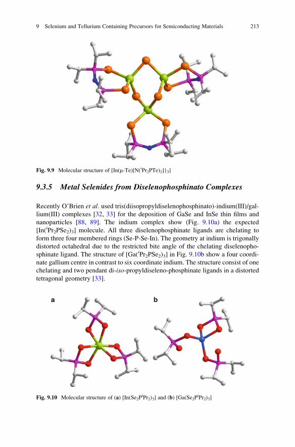
9.3.5 Metal Selenides from Diselenophosphinato Complexes
Recently O’Brien et al. used tris(diisopropyldiselenophosphinato)-indium(III)/gal-
lium(III) complexes [32, 33] for the deposition of GaSe and InSe thin films and
nanoparticles [88, 89]. The indium complex show (Fig. 9.10a) the expected
[In(iPr2PSe2)3] molecule. All three diselenophosphinate ligands are chelating to
form three four membered rings (Se-P-Se-In). The geometry at indium is trigonally
distorted octahedral due to the restricted bite angle of the chelating diselenopho-
sphinate ligand. The structure of [Ga(iPr2PSe2)3] in Fig. 9.10b show a four coordi-
nate gallium centre in contrast to six coordinate indium. The structure consist of one
chelating and two pendant di-iso-propyldiseleno-phosphinate ligands in a distorted
tetragonal geometry [33].
Fig. 9.9 Molecular structure of [In(m-Te)[N(iPr2PTe)2]}3]
Fig. 9.10 Molecular structure of (a) [In(Se2PiPr2)3] and (b) [Ga(Se2P
iPr2)3]
9 Selenium and Tellurium Containing Precursors for Semiconducting Materials 213
9.4 IV–VI Materials
9.4.1 Lead Selenides/Tellurides
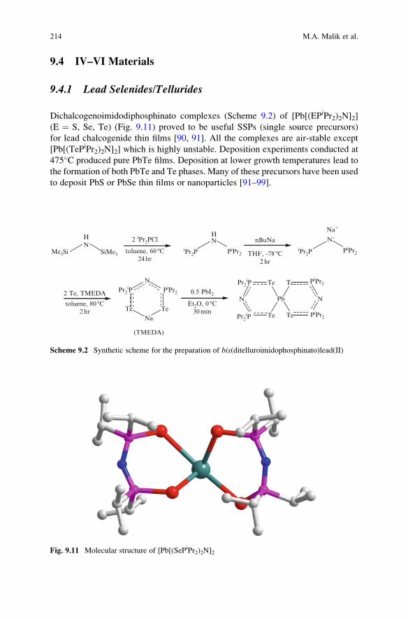
Dichalcogenoimidodiphosphinato complexes (Scheme 9.2) of [Pb[(EPiPr2)2N]2]
(E ¼ S, Se, Te) (Fig. 9.11) proved to be useful SSPs (single source precursors)
for lead chalcogenide thin films [90, 91]. All the complexes are air-stable except
[Pb[(TePiPr2)2N]2] which is highly unstable. Deposition experiments conducted at
475�C produced pure PbTe films. Deposition at lower growth temperatures lead to
the formation of both PbTe and Te phases. Many of these precursors have been used
to deposit PbS or PbSe thin films or nanoparticles [91–99].
Me3Si
HN
SiMe3
2 iPr2PCl
toluene, 60 ºC24hr
iPr2PiPr2P
HN
PiPr2PiPr2
nBuNa
THF, -78 ºC2hr
N-
Na+
2 Te, TMEDA
toluene, 80 ºC2hr
Pr2iP
Pr2iP
Pr2iP
Te
Na
Te
PiPr2
PiPr2
PiPr2
N
(TMEDA)
0.5 PbI2
Et2O, 0 ºC30min
Te
N
Te
Pb
Te
N
Te
Scheme 9.2 Synthetic scheme for the preparation of bis(ditelluroimidophosphinato)lead(II)
Fig. 9.11 Molecular structure of [Pb[(SePiPr2)2N]2
214 M.A. Malik et al.
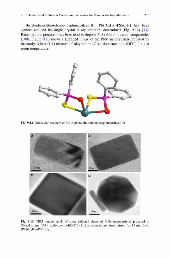
Bis(di-phenylthioselenophosphinato)lead(II) [Pb{(C6H5)2PSSe)}2] has been
synthesised and its single crystal X-ray structure determined (Fig. 9.12) [33].
Recently, this precursor has been used to deposit PbSe thin films and nanoparticles
[100]. Figure 9.13 shows a HRTEM image of the PbSe nanocrystals prepared by
thermolysis in a (1:1) mixture of oleylamine (OA): dodecanethiol (DDT) (1:1) at
room temperature.
Fig. 9.12 Molecular structure of bis[di-phenylthioselenophosphinato)]lead(II)
10nm 10nm
10nm 10nm
a b
c d
Fig. 9.13 TEM images (a–d) of some selected shape of PbSe nanoparticles prepared in
Oleyal amine (OA): dodecanethiol(DDT) (1:1) at room temperature stirred for 15 min from
[Pb{(C6H5)2PSSe)}2]
9 Selenium and Tellurium Containing Precursors for Semiconducting Materials 215
The deposition of PbSe thin films from diselenophosphinato- and imidodisele-
nodiphosphinato-lead complexes [90, 91] always results in contamination of
phosphorous. In order to overcome this problem, O’Brien et al. have synthesized
(4-nitro-N,N-di-iso-butyl-N-benzoylselenoureato)Pb(II) andN,N-diethyl-N-benzoylse-lenoureato) Pb(II) complexes to be used as SSP for the deposition of PbSe thin
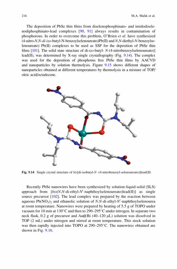
films [101]. The solid state structure of di-iso-butyl- N-(4-nitrobenzoylselenoureato)]lead(II), was determined by X-ray single crystallography (Fig. 9.14). The complex
was used for the deposition of phosphorus free PbSe thin films by AACVD
and nanoparticles by solution thermolysis. Figure 9.15 shows different shapes of
nanoparticles obtained at different temperatures by thermolysis in a mixture of TOP/
oleic acid/octadecene.
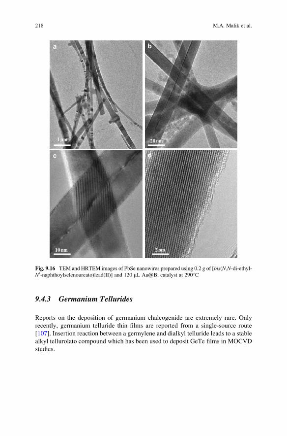
Recently PbSe nanowires have been synthesized by solution-liquid-solid (SLS)
approach from [bis(N,N-di-ethyl-N0-naphthoylselenoureato)lead(II)] as single
source precursor [102]. The lead complex was prepared by the reaction between
aqueous Pb(NO3)2 and ethanolic solution of N,N-di-ethyl-N0-naphthoylselenoureaat room temperature. Nanowires were prepared by heating of 5.5 g of TOPO under
vacuum for 10 min at 130�C and then to 290–295�C under nitrogen. In separate two
neck flask, 0.2 g of precursor and Au@Bi (40–120 mL) solution was dissolved in
TOP (2 mL) under nitrogen and stirred at room temperature. This stock solution
was then rapidly injected into TOPO at 290–295�C. The nanowires obtained are
shown in Fig. 9.16.
Fig. 9.14 Single crystal structure of bis[di-isobutyl-N -(4-nitrobenzoyl-selenoureato)]lead(II)
216 M.A. Malik et al.

9.4.2 Tin Selenides/Tellurides
Dahmen and co-workers have used bis[bis(trimethylsilyl)methyl]tin chalcogenides,
[Sn{CH(SiMe3)2}2(m�E)]2 (E ¼ Se, Te) for the MOCVD of SnSe and SnTe thin
films [103, 104]. These complexes are dimers in solution as well as in the solid
state. The compounds are air-stable and volatile [105]. MOCVD experiments
indicated that both compounds show strong selectivity in the decomposition reac-
tion towards the metallic substrates, thus demonstrating the need for a seeding
metallic layer to initiate the growth. In the case of non-metallic substrates, no film
deposition was obtained under all experimental conditions.
The [SnCl4{o-C6H4(CH2SeMe)2}] deposits poor quality SnSe2 films at 600�C.The Et2Se derivative, [SnCl4(Et2Se)2] leads to uniform deposition of SnSe2 with
growth perpendicular to the substrate [106].
Fig. 9.15 (a, b) TEM image and HRTEM image of spherical shape PbSe nanoparticles prepared
from bis[di-isobutyl-N-(4-nitrobenzoylseleno-ureato)]lead(II)at 200�C, (c, d) cubic shape PbSe
nanoparticles prepared at 250�C (all in TOP/oleic acid/octadecene)
9 Selenium and Tellurium Containing Precursors for Semiconducting Materials 217
9.4.3 Germanium Tellurides
Reports on the deposition of germanium chalcogenide are extremely rare. Only
recently, germanium telluride thin films are reported from a single-source route
[107]. Insertion reaction between a germylene and dialkyl telluride leads to a stable
alkyl tellurolato compound which has been used to deposit GeTe films in MOCVD
studies.
c d
a b
1µm
2nm10nm
20nm
Fig. 9.16 TEM and HRTEM images of PbSe nanowires prepared using 0.2 g of [bis(N,N-di-ethyl-N0-naphthoylselenoureato)lead(II)] and 120 mL Au@Bi catalyst at 290�C
218 M.A. Malik et al.

9.5 V–VI Materials
9.5.1 Antimony Selenides/Tellurides
The V–VI materials attracted a considerable interest due to their thermo-electric
and photovoltaic properties which find applications in thermo-electric and
optoelectronic devices [108–111], television cameras [113, 114], and solar cells
[115]. While there are several reports on V–VI metal sulfides [116–121], the work
on metal selenides has recently started [122]. Previously the selenides have been
prepared by heating elements (Sb/Bi and Se) at high temperatures [123–125].
Recently other techniques, such as solvothermal, hydrothermal, microwave assisted
synthesis and chemical bath deposition have been used to prepare thin films and
nanoparticles [126–130]. There are only few examples of using single source
precursors for the preparation of V–VI materials [131–134]. The preparation of
Sb2Se3 nanowires from [Sb{Se2P(OiPr)2}3] under solvothermal conditions has been
reported by Chang et al. [131]. In a later study the authors have studied the
electrical and optical properties of a single Sb2Se3 nanorod with an average size
of 70 nm in diameter and a length of ~1–2 mm [135]. Recently complexes with the
general formula [M{Se–C5H3(R-3)N}3] (M ¼ Sb or Bi) have been prepared by the
reaction of SbCl3 or BiCl3 with M0Se–C5H3(R-3)N (M0 ¼ Li or Na; R ¼ H or Me)
and the molecular structures of both complexes have been determined by X-ray
crystallography (Fig. 9.17a, b) [136].
The structure of antimony complex (Fig. 9.17a) is monomer in which antimony
atom is bonded to three selenolates of monodentate Se–C5H3(Me-3)N ligands to
acquire a trigonal pyramidal configuration. The void in the coordination sphere of
Fig. 9.17 Molecular structures of (a) Sb{Se–C5H3(Me-3)N}3]; (b) Bi{Se–C5H3(Me-3)N}3]
9 Selenium and Tellurium Containing Precursors for Semiconducting Materials 219

antimony can be viewed conventionally as filled by a stereochemically active lone
pair of electrons. The structure of the bismuth complex (Fig. 9.17b) is based on
a distorted square pyramidal configuration by two chelating and a monodentate
selenolate ligands. The monodentate ligand occupies the apical position and the
position opposite is filled by stereochemically active lone pair of electrons, while
the two chelating ligands occupy the corners of the square. Pyrolysis of antimony and
bismuth complexes at 400�C and 450�C for 1 h under argon in a furnace produced
black residues which were characterized by pXRD and SEM as orthorhombic Sb2Se3rods (Fig. 9.18) and hexagonal BiSe flowers (Fig. 9.19) whereas thermolysis of these
complexes in HDA provided orthorhombic Sb2Se3 and rhombohedral Bi2Se3 [136].
Thin films of these materials were also obtained by AACVD method.
The homoleptic antimony(III) complex [Sb[(TePiPr2)2N)2]3] (Fig. 9.20) have
been used as single source precursor by O’Brien et al. to prepare hexagonal-shapednanoplates of pure rhombohedral Sb2Te3 thin films by AACVD method in the
temperature range 375–475�C [134].
9.5.2 Bismuth Selenides
Bismuth chalcogenide films have been reported from CVD studies of air-stable
complexes of Bi[(EPR2)2N]3 (E ¼ S, Se; R ¼ Ph, iPr) [133]. The compounds were
prepared using methodology developed byWoollins et al. (Scheme 9.3) [67]. These
neutral ligands are readily deprotonated to the monoanions by treatment with bases
such as sodium methoxide. Subsequent metathetical reactions with metal halides
produce homoleptic complexes in good yields.
Fig. 9.18 SEM images of Sb2Se3 nanorods obtained by pyrolysis of [Sb{Se–C5H3(Me-3)N}3] (2)
in a furnace at 400�C for 1 h
220 M.A. Malik et al.

Fig. 9.20 Molecular structure of [Sb[(TePPri2)2N)2]3]
Fig. 9.19 (a–d) SEM images of different magnifications of BiSe flowers obtained by pyrolysis of
[Bi{Se–C5H3(Me-3)N}3] at 450�C for 1 h, respectively
9 Selenium and Tellurium Containing Precursors for Semiconducting Materials 221

Crystalline thin films of rhombohedral Bi2Se3 (from Bi[(SePiPr2)2N]3), hexago-
nal BiSe (from Bi[(SePPh2)2N]3, and orthorhombic Bi2S3 (from Bi[(SPR2)2N]3have been deposited on glass substrates [133]. The suggested reason for the
deposition of monophasic Bi2Se3 and BiSe from isopropyl and phenyl substituted
precursors, respectively is that the difference in electron-donating character of the
alkyl group on the P atoms affects the relative bond strengths within the structures
and hence the decomposition profiles of the parent molecules.
Thin films composed of hexagonal Bi2Se3 nanoplates have also been deposited
from MOCVD of bismuth diselenophosphato complex, [Bi(Se2P{OiPr)2}3] on
modified and unmodified Si substrates [137]. The deposited Bi2Se3 nanoplates
indicate a superior thermoelectric property over bulk Bi2Se3.
9.6 The CIS and CIGS Family of Materials
Compound semiconducting materials of the I-III-VI2 family such as CuInSe2 (CIS),
CuGaSe2 and CuIn(1�x)GaxSe2 (CIGS) are amongst the leading candidate absorber
materials for photovoltaic applications. The attraction chalcopyrite based I-III-VI2photovoltaic materials lies in their high conversion efficiency, higher absorption
coefficients, photo-irradiation stability and lower toxicity [138, 139]. CuInSe2 has a
direct bandgap of 1.04 eV which can be further broadened by incorporation of Ga
leading to formation of CuInGaSe2 (CIGS). The bandgap of the materials, generally
as represented by CuIn(1�x)GaxSe2, can be tuned from 1.04 to 1.68 eV by controlled
substitution of Ga for In atoms [140].
Previously we have reported synthesis of CuInSe2 nanoparticles by a two step
reaction using CuCl, InCl3 and TOPSe in TOPO [141]. Castro and co-workers have
synthesized chalcopyrite semiconductor nanoparticles of CuInS2 and CuInSe2 by
thermal decomposition of ternary molecular single source precursors (PPh3)2CuIn
(SEt)4 and (PPh3)2CuIn(SePh)4 in dioctyl phthalate at temperatures from 200�C to
300�C [142]. Allan and Bawendi have reported the synthesis of Cu-In-Se quantum
dots of varying stoichiometric compositions, which exhibited high photolumine-
scence quantum yields (PLQY) from the red to near infrared (NIR) region [143].
R2P PR2
HN 2 E
HN
R2P
E E
PR2NaOMe
N
R2P
E E
PR2
E = S, R = PhE = S, R = Pri
E = Se, R = PhE = Se, R = Pri
–
Scheme 9.3 Synthetic scheme for the preparation of dichalcogenoimidophosphinato ligand
222 M.A. Malik et al.
Their approach involved the use of the metal halides of copper and indium
precursors and bis(trimethylsilyl)selenide [(Me3Si)2Se] as the chalcogenide precur-
sor, whereas a combination of tri-n-octylphosphine (TOP) and oleylamine (OA)
was used as a coordinating solvent and capping ligand. However, the stoichiometric
compositions obtained were not CuInSe2 but materials of stoichiometry CuIn5Se8,
CuIn2.4Se4, and CuIn1.5Se3.
CuInSe2, CuGaSe2 and CuIn(1�x)GaxSe2 (CIGS) nanoparticles were deposited
from the diisopropyldiselenophosphinatometal complexes Mx[iPr2PSe2]y (M ¼ Cu,
In, Ga) by thermal decomposition of precursors in HDA/TOP system at 120–210�Cand 250�C, respectively [89]. The semiconductor nanoparticles obtained were
characterized by X-ray diffraction (XRD), scanning electron microscopy (SEM),
transmission electron microscopy (TEM) and energy dispersive X-ray (EDX) analy-
sis. Figure 9.21 shows the TEM images and SAED pattern and a histogram
representing size distribution of tetragonal CuIn0.7Ga0.3Se2 nanoparticles.
The corresponding diisopropyldiselenophosphinatometal complexesMx[iPr2PSe2]y
(M ¼ Cu, In, Ga) were also used to deposit CuSe, g-In2Se3, CuInSe2, CuGaSe2,and CuIn0.7Ga0.3Se2, thin films by AA-CVD method. Figure 9.22 shows SEM
images of as deposited (a) g-In2Se3 thin film at 450�C (b) CuGaSe2 thin at 300�C(b) 500�C (d) 3D AFM image of CuGaSe2 thin films at 450�C from 1:4 equivalent
of [Cu4(iPr2P2Se2)4] and [Ga(iPr2PSe2)3]. Figure 9.23 shows SEM images of as
Fig. 9.21 (a–d) TEM images of tetragonal CuIn0.7Ga0.3Se2 quantum dots (e) SAED pattern of the
CuIn0.7Ga0.3Se2 nanoparticles and (f) histogram representing size distribution for CuIn0.7Ga0.3Se2quantum dots
9 Selenium and Tellurium Containing Precursors for Semiconducting Materials 223

dμm/div
μm/div
0.072
0
0.20
μm/div0.20
Fig. 9.22 SEM images of as deposited (a) g-In2Se3 thin film at 450�C (b) CuGaSe2 thin at 300�C
(b) 500�C (d) 3D AFM image of as grown CuGaSe2 thin films at 450�C from 1:4 equivalent of
[Cu4(iPr2P2Se2)4] and [Ga(iPr2PSe2)3]
Fig. 9.23 SEM images of as deposited CuIn0.7Ga0.3Se2 at (a) 300�C, (b) 350�C, (c) 400�C and
(d) 450�C from 1:4:4 equivalent of [Cu4(iPr2P2Se2)4], [In(iPr2PSe2)3] and [Ga(iPr2PSe2)3],
respectively
224 M.A. Malik et al.

deposited CuIn0.7Ga0.3Se2 at different temperatures from 1:4:4 equivalent of
[Cu4(iPr2P2Se2)4], [In(
iPr2PSe2)3] and [Ga(iPr2PSe2)3] respectively.
9.7 Transition Metal Selenides and Tellurides
9.7.1 Nickel and Cobalt Selenides
Air-stable, metal-organic compounds of the type [M{iPr2P(S)NP(Se)iPr2}2], (M ¼
Ni, Co) were synthesised by the metathetical reaction between the sodium salt of
the S/Se containing imidodiphosphinate ligand with the appropriate metal salt in
methanol and the structure of cobalt complex was determined by X-ray crystallog-
raphy [144]. Both compounds are monomeric and isomorphous with tetrahedral
coordination geometry at the metal centre. These compounds have been used as
single-source precursors to deposit thin films of metal phosphide or selenide by
AA-CVD and LP-CVD methods. The mechanism of the unique formation of
phosphide or selenide films from the same precursor was studied by pyrolysis
GC-MS and by ab initio computational studies [144].
Diisopropylimidodiselenophosphinato complexes [Ni[(SePiPr2)2N]2], [Co
[(SePiPr2)2N)2] and diisopropyldiselenophosphinato [Ni(Se2PiPr2)2] and [Co
(Se2PiPr2)2] were synthesized and the single crystal X-ray structures of Ni
[(SePiPr2)2N]2 and [Ni(Se2PiPr2)2] were determined [145]. All these compounds
were used to deposit thin films of nickel and cobalt selenide by CVD.
The recrystallisation of [Ni[(SePiPr2)2N)]2] from THF solution at room temper-
ature gave deep red and green colour crystals. Single crystal X-ray structure of the
red crystals showed the nickel in tetrahedral geometry whereas in square planar
geometry in green crystals (Fig. 9.24a, b). The square planar geometry also showed
the presence of a molecule of water in partial occupancy in the crystal lattice.
The diselenophosphinato nickel complexes are square planar (Fig. 9.25). The Ni
atoms are surrounded by a distorted square of four Se atoms belonging to two
bidentate chelating ligands as in the iPr2PSe2 complex.
Fig. 9.24 X-ray crystal structure of Ni[(SePiPr2)2N]2 (a) tetrahedral and (b) square planar
9 Selenium and Tellurium Containing Precursors for Semiconducting Materials 225

The deposition by AA-MOCVD from Ni[(SePiPr2)2N]2 produced uniform black
films at temperatures between 400�C and 500�C. XRD studies show that in each
case, monophasic hexagonal Ni0.85Se was deposited, with preferred orientation in
the (101) direction. SEM studies revealed that the films comprise of mixtures
of fibrous wires and rods. The morphology of the films change from thin and
short wires to thicker and longer wires as the deposition temperatures increases
(Fig. 9.26a–d).
Deposition from [Ni(Se2PiPr2)2] gave thick black films at 350�C, 400�C and
450�C. XRD results showed that all films were composed of hexagonal Ni0.85Se
with preferred growth along (101) plane. SEM images showed that morphologies
Fig. 9.25 X-ray crystal structure of [Ni(iPr2PSe2)2]
a
c
b
d
2 μm 2 μm
2 μm2 μm
Fig. 9.26 SEM images of nickel selenide films deposited on glass from [Ni{(SePiPr2)2N}2] at (a)
425�C, (b) 450�C, (c) 475�C and (d) 500�C
226 M.A. Malik et al.

varied from a mixture of cubic crystallites and flakes at 350�C to spherical particles
connected by wires at 400�C. Deposition from [Co(Se2PiPr2)2] by AA-MOCVD
gave thick black films at 450�C. No deposition was obtained at lower temperatures.
The films consits of a mixture of Co9Se8 and CoP phases as revealed by XRD
analysis. The morphology appears to be irregular grains of varing sizes. Deposition
of thin films was also carried out from selenophosphinato nickel/cobalt(II) and the
results were compared to imidoselenophosphinato nickel/cobalt(II) and seleno-
phophinato nickel/cobalt(II).
9.7.2 Copper/Silver Selenides/Tellurides
A series of dichalcogenophosphinato and imidodichalcogenodiphosphinato silver
(I) complexes including [Ag(Se2PiPr2)], [Ag4(SSeP
iPr2)4], [Ag{iPr2P(S)NP
(Se)iPr2}]3 and [Ag(SePiPr2)2N]3 have been synthesised and structures of
[Ag4(SSePiPr2)4] and [Ag{iPr2P(S)NP(Se)
iPr2}]3 were determined by X-ray single
crystallography [146]. The structure of [Ag4(SSePiPr2)4] consists of tetrahedral
array of four Ag(I) atoms capped by four bidentate [iPr2PSSe] ligands coordinated
to the Ag atoms through S or Se atoms (Fig. 9.27).
Each ligand caps one triangular face of the Ag(I) tetrahedrons by one bridging
and one terminal chalcogen atom. Each Ag atom has coordination number of five
with distorted trigonal distribution. The molecular structure of [Ag{iPr2P(S)NP
Fig. 9.27 Molecular structure of [Ag4(SSePiPr2)4]
9 Selenium and Tellurium Containing Precursors for Semiconducting Materials 227

(Se)iPr2}]3 shows a trimeric unit along with toluene as solvate (Fig. 9.28) similar to
that of the silver-selenium analogue [Ag(SePiPr2)2N]3 [63].
All four compounds were used as single-source precursors for the deposition of
silver selenide thin films by AA-CVD and LP-CVD methods. All precursors gave
silver selenide (Ag2Se) films by AACVD; whereas only [Ag{iPr2P(S)NP(Se)iPr2}]3
and [Ag(SePiPr2)2N]3 gave silver selenide films by LPCVD.
Films deposited from [Ag{iPr2P(S)NP(Se)iPr2}]3 at 325�C were mainly com-
posed of monodispersed spherical silver selenide nanoparticles (0.05–0.1 mm) but a
significant change in morphology occurred at higher deposition temperatures
(375–475�C) (Fig. 9.29). Films deposited at all temperatures were silver deficient
and selenium rich.
Metal ditelluroimidodiphosphinate complexes {Cu[N(TePiPr2)2]}3, {Ag[N
(TePiPr2)2]}6, Au(PPh3)[N(TePiPr2)2] and in {Ag[N(TePPh2)2}4·2THF have been
prepared by the reactions of Na(tmeda)[N(TePiPr2)2] in THF solution with CuCl,
AgI or AuCl respectively [147]. X-ray structures single crystal structure of {Cu[N
(TePiPr2)2]} (Fig.9.30) consists of three six membered CuTe2P2N rings, which are
linked together to form two central, highly distorted Cu3Te3 rings.
The distortion of these central rings results in surprisingly short copper–copper
distances of 2.626(1) and 2.637(2) A. Two of the ligands are equivalent with similar
metrical parameters, each containing one tellurium which is complexed to one
copper centre and one tellurium bridging two copper centres.
Structure of {Ag[N(TePiPr2)2]}6 consists of six Ag[N(TePiPr2)2] units to give
the hexamer (Fig. 9.31). The molecule lies on an inversion centre so the two halves
Fig. 9.28 Molecular structure of [Ag{iPr2P(S)NP(Se)iPr2}]3
228 M.A. Malik et al.

Fig. 9.29 SEM images of silver selenide films deposited on glass by AACVD from [Ag{iPr2P(S)
NP(Se)iPr2}]3 at flow rate of 160 sccm and growth temperatures of (a) 325�C, (b) 375�C, (c)425�C and (d) 475�C
Fig. 9.30 Molecular structure of [Cu{N(iPr2PTe)2}]3
9 Selenium and Tellurium Containing Precursors for Semiconducting Materials 229

of the hexamer are crystallographically equivalent. The silver centres are each
bound to two tellurium centres from one ligand and one tellurium from an adjacent
Ag[N(TePiPr2)2] moiety. Each silver centre is coordinated equally between two
bridging tellurium centres of adjacent [N(TePiPr2)2] ligands forming a central
Fig. 9.31 Molecular structure of [Ag{N(iPr2PTe)2}]6
Fig. 9.32 Molecular structure of {Ag[N(Ph2PTe)2]}4
230 M.A. Malik et al.
twelve membered Ag6Te6 ring. The replacement of the iPr groups on phosphorus by
Ph results in a tetramer with a boat-shaped Ag4Te4 ring in [Ag{N(Ph2PTe)2}4]·2THF
(Fig. 9.32).
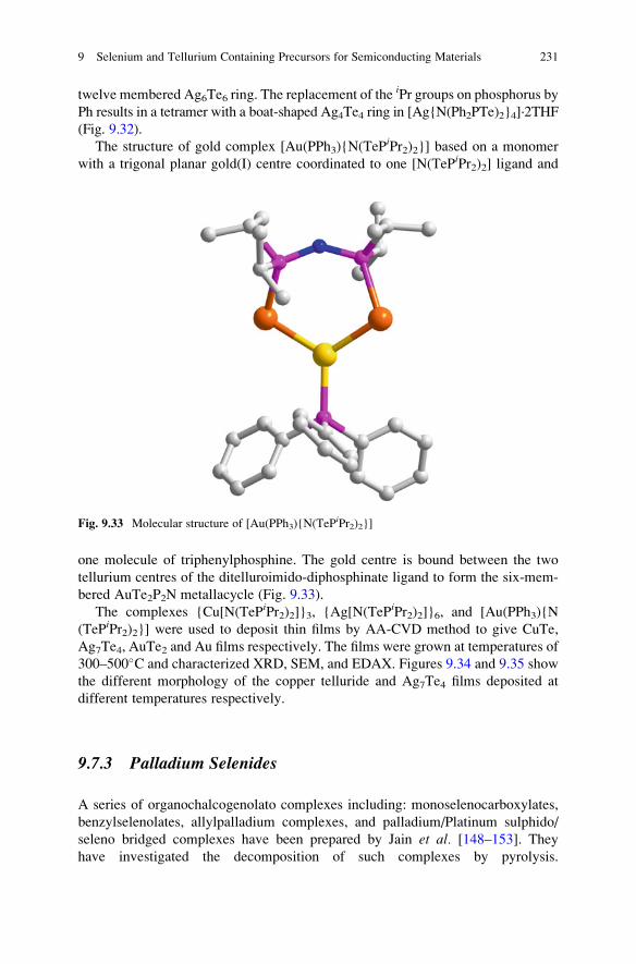
The structure of gold complex [Au(PPh3){N(TePiPr2)2}] based on a monomer
with a trigonal planar gold(I) centre coordinated to one [N(TePiPr2)2] ligand and
one molecule of triphenylphosphine. The gold centre is bound between the two
tellurium centres of the ditelluroimido-diphosphinate ligand to form the six-mem-
bered AuTe2P2N metallacycle (Fig. 9.33).
The complexes {Cu[N(TePiPr2)2]}3, {Ag[N(TePiPr2)2]}6, and [Au(PPh3){N
(TePiPr2)2}] were used to deposit thin films by AA-CVD method to give CuTe,
Ag7Te4, AuTe2 and Au films respectively. The films were grown at temperatures of
300–500�C and characterized XRD, SEM, and EDAX. Figures 9.34 and 9.35 show
the different morphology of the copper telluride and Ag7Te4 films deposited at
different temperatures respectively.
9.7.3 Palladium Selenides
A series of organochalcogenolato complexes including: monoselenocarboxylates,
benzylselenolates, allylpalladium complexes, and palladium/Platinum sulphido/
seleno bridged complexes have been prepared by Jain et al. [148–153]. Theyhave investigated the decomposition of such complexes by pyrolysis.
Fig. 9.33 Molecular structure of [Au(PPh3){N(TePiPr2)2}]
9 Selenium and Tellurium Containing Precursors for Semiconducting Materials 231

The decomposition of [M2Cl2(m�SenPr)2(PnPr3)2] in tributylphosphate at 195�C
gave Pd17Se15 whereas the pyrolysis of related allylpalladium complexes in xylene
gave Pd4Se19 [154–156]. In another study Pd(acac)2 (or PdCl2) was reacted with
nanowires of trigonal selenium (t-Se, as a template) in refluxing ethanol to generate
Pd17Se15 on the surface of each t-Se nanowire. Recently for the first time a single
source precursor [bis(N,N-diethyl-N0-naphthoylselenoureato)palladium(II)] was
used to deposit thin films by AACVD at deposition temperatures of 400–500�Cand nanoparticles by colloidal method [157].
Fig. 9.35 SEM images of Ag7Te4 films deposited at (a) and (b) 300�C, (c) 350�C, (d) 400�C, (e)450�C and (f) 500�C. The inset in (b) shows the SAED of truncated hexagonal plates. The inset in
(f) shows the morphology of the film at 450�C after etching
Fig. 9.34 SEM images of copper telluride films deposited at (a) 300�C, (b) 350�C, (c) 400�C, (d)450�C and (e) 500�C
232 M.A. Malik et al.
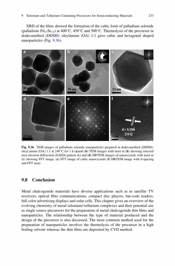
XRD of the films showed the formation of the cubic form of palladium selenide
(palladisite Pd17Se15) at 400�C, 450�C and 500�C. Thermolysis of the precursor in
dodecanethiol (DDSH): oleylamine (OA) 1:1 gave cubic and hexagonal shaped
nanoparticles (Fig. 9.36).
9.8 Conclusion
Metal chalcogenide materials have diverse applications such as in satellite TV
receivers, optical fibre communications, compact disc players, bar-code readers,
full color advertising displays and solar cells. This chapter gives an overview of the
evolving chemistry of metal selenium/-tellurium complexes and their potential use
as single source precursors for the preparation of metal chalcogenide thin films and
nanoparticles. The relationship between the type of material produced and the
design of the precursor is also discussed. The most common method used for the
preparation of nanoparticles involves the thermolysis of the precursor in a high
boiling solvent whereas the thin films are deposited by CVD method.
Fig. 9.36 TEM images of palladium selenide nanoparticles prepared in dodecanethiol (DDSH):
oleyl amine (OA) 1:1 at 240�C for 1 h (a)and (b) TEM images with inset in (b) showing selected
area electron diffraction (SAED) pattern (c) and (d) HRTEM images of nanocrystals with inset in
(c) showing FFT image. (e) FFT image of cubic nanocrystals (f) HRTEM image with d-spacing
and FFT inset
9 Selenium and Tellurium Containing Precursors for Semiconducting Materials 233

References
1. Malik MA, Afzaal M, O’Brien P (2010) Chem Rev 110:4417–4446
2. Malik MA, Afzaal M, O’Brien P (2010) J Mater Chem 20:4031–4040
3. Trindade T, O’Brien P, Pickett NL (2001) Chem Mater 13:3843–3858
4. Pickett NL, O’Brien P (2001) Chem Rec 1:467–479
5. O’Brien P (1991) Chemtronics 5:61–70
6. O’Brien P, Nomura R (1995) J Mater Chem 5:1761–1773
7. Bochmann M (1996) Chem Vap Deposition 2:85–96
8. Boyle DS, Hearne S, Johnson DR, O’Brien P (1999) J Mater Chem 9:2879–2884
9. Park JH, Afzaal M, Kemmler M, O’Brien P, Otway DJ, Raftery J, Waters J (2003) J Mater
Chem 13:1942–1949
10. Ahmad K, Afzaal M, O’Brien P, Hua GH, Woollins DJ (2010) Chem Mater 22:4619–4624
11. Ma W, Luther JM, Zheng H, Wu Y, Alivisatos P (2009) Nano Lett 9:1699–1703
12. Manasevi HM (1981) J Cryst Growth 55:10–23
13. Brennan JG, Segrist T, Carroll PJ, Stuczynski SM, Reynders P, Brus LE, Steigerwald ML
(1989) J Am Chem Soc 111:4141–4143
14. Brennan JG, Siegrist T, Carroll PJ, Stuczynski SM, Reynders P, Brus LE, Steigerwald ML
(1990) Chem Mater 2:403–409
15. Osakada K, Yamamoto T (1987) J Chem Soc Chem Commun 1117–1118
16. Steigerwald ML, Sprinkle CR (1987) J Am Chem Soc 109:7200–7201
17. Zeng D, Hampden-Smith MJ, Densler EN (1994) Inorg Chem 33:5376–5377
18. Bochmann M, Webb K, Harman M, Hursthouse MB (1990) Angew Chem Int Ed Engl
29:638–639
19. Bochmann M, Webb KJ, Hursthouse MB, Mazid M (1991) J Chem Soc Dalton Trans
2317–2323
20. Bochmann M, Webb KJ (1991) J Chem Soc Dalton Trans 9:2325–2329
21. Bochmann M, Bwembya GC, Grinter R, Powell AK, Webb KJ, Hursthouse MB, Abdel
Malik KM, Mazid MA (1994) Inorg Chem 33:2290–2296
22. Bochmann M, Webb KJ (1991) Mater Res Soc Symp Proc 204:149–154, Chem. Abstr 1992,
116, 33194h
23. Bochmann M, Webb KJ, Hails J-E, Wolverson D (1992) Eur J Solid State Inorg Chem
29:155–166
24. Bochmann M, Coleman AP, Powell AK (1992) Polyhedron 11:507–512
25. Jun YW, Choi CS, Cheon J (2001) Chem Commum 101–102
26. Dabbousi BO, Bonasia PJ, Arnold J (1991) J Am Chem Soc 113:3186–3188
27. Bonasi PJ, Arnold J (1992) Inorg Chem 31:2508–2514
28. Arnold J, Walker JM, Yu KM, Bonasia PJ, Seligson AL, Bourret ED (1992) J Cryst Growth
124:647–653
29. Bonasia PJ, Gindelberger DE, Dabbousi BO, Arnold J (1992) J Am Chem Soc
114:5209–5214
30. Bonasia PJ, Mitchell GP, Hollander FJ, Arnold J (1994) Inorg Chem 33:1797–1802
31. Arnold J, Bonasia PJ (1992) US Pat 5157136; Chem. Abstr. 1993, 118, 213295s
32. Adeogun A, Nguyen CQ, Afzaal M, Malik MA, O’Brien P (2006) Chem Commun
2179–2181
33. Nguyen CQ, Adeogun A, Afzaal M, Malik MA, O’Brien P (2006) Chem Commun
2182–2184
34. Klug HP (1966) Acta Crystallogr 21:536–546
35. Bonamico M, Mazzone G, Vaciago A, Zambonelli L (1965) Acta Crystallogr 19:898–909
36. Miyame H, Ito M, Iwasaki H (1979) Acta Crystallogr B B35:1480–1482
37. Domenicano A, Torelli L, Vaciago A, Zambonelli L (1968) J Chem Soc A 1351–1361
38. Bonamico M, Dessy G (1971) J Chem Soc A 264–26939. Hursthouse MB, Malik MA, Motevalli M, O’Brien P (1992) Polyhedron 11:45–48
234 M.A. Malik et al.

40. Motevalli M, O’Brien P, Walsh JR, Watson IM (1996) Polyhedron 15:2801–2808
41. Chunggaze M, McAleese J, O’Brien P, Otway DJ (1998) J Chem Soc Chem Commun
7:833–834
42. O’Brien P, Otway DJ, Walsh JR (1997) Adv Mater CVD 3:227–229
43. Chunggaz M, Malik MA, O’Brien P (1999) J Mater Chem 9:2433–2437
44. Ludolph B, Malik MA, O’Brien P, Revaprasadu N (1998) Chem Commun 17:1849–1850
45. Malik MA, O’Brien P (1994) Adv Mater Opt Electron 3:171–175
46. Hursthouse MB, Malik MA, Motevalli M, O’Brien P (1992) J Mater Chem 9:949–955
47. Noltes JG (1965) Recl Trav Chim Pay-B 84:126
48. Hursthouse MB, Malik MA, Motevalli M, O’Brien P (1991) Organometallics 10:730–732
49. Nyman M, Hampden-Smith MJ, Duesler E (1996) Chem Vap Deposition 2:171–174
50. Nyman M, Jenkins K, Hampden-Smith MJ, Kodas TT, Duesler EN, Rheingold AL,
Liable-Sands ML (1998) Chem Mater 10:914–921
51. Schmidpeter A, Bohm R, Groeger H (1964) Angew Chem Int Ed Engl 3:704
52. Schmidpeter A, Stoll K (1967) Angew Chem Int Ed Engl 6:252–253
53. Schmidpeter A, Stoll K (1968) Angew Chem Int Ed Engl 7:549–550
54. Malik MA, O’Brien P (1991) Chem Mater 3:999–1000
55. Malik MA, Motevalli M, O’Brien P, Walsh JR (1992) Organometallics 11:3136–3139
56. Abrahams I, Malik MA, Motevalli M, O’Brien P (1994) J Organomet Chem 465:73–77
57. Malik MA, Motevalli M, O’Brien P (1996) Acta Crystallogr C C52:1931–1933
58. Bhattacharyya P, Slawin AMZ, Williams DJ, Woollins JD (1995) J Chem Soc, Dalton Trans
2489–2495
59. Silvestru C, Drake JE (2001) Coord Chem Rev 223:117–216
60. Ly TQ, Woollins JD (1998) Polyhedron 176:451–480
61. Afzaal M, Crouch D, Malik MA, Motevalli M, O’Brien P, Park J-H, Woollins JD (2004) Eur
J Inorg Chem 171–177
62. Crouch DJ, O’Brien P, Malik MA, Skabara PJ, Wright SP (2003) Chem Commun
1454–1455
63. Afzaal M, Crouch DJ, O’Brien P, Raftery J, Skabara PJ, White AJP, Williams DJ (2004)
J Mater Chem 14:233–237
64. Dance IG, Choy A, Scudder ML (1984) J Am Chem Soc 106:6285–6295
65. Lee GSH, Fisher KJ, Craig DC, Scudder M, Dance IG (1990) J Am Chem Soc
112:6435–6437
66. Cumberland SL, Hanif KM, Javier A, Khitrov GA, Strouse GF, Woessner SM, Yun CS
(2002) Chem Mater 14:1576–1584
67. Cupertino D, Birdsall DJ, Slawin AMZ, Woollins JD (1999) Inorg Chim Acta 290:1–7
68. Afzaal M, Aucott SM, Crouch D, O’Brien P, Woollins JD, Park JH (2002) Chem Vap
Deposition 8:187–189
69. Afzaal M, Crouch D, O’Brien P, Park JH (2002) Mater Res Soc Symp Proc 692–698
70. Afzaal M, Crouch D, Malik MA, Motevalli M, O’Brien P, Park JH, Woollins JD (2004) Eur
J Inorg Chem 171–177
71. Afzaal M, Crouch D, Malik MA, Motevalli M, O’Brien P, Park JH (2003) J Mater Chem
13:639–640
72. Garje SS, Ritch JS, Eisler DJ, Afzaal M, O’Brien P, Chivers T (2006) J Mater Chem
16:966–969
73. Briand GG, Chivers T, Parvez M (2002) Angew Chem Int Ed 41:3468–3470
74. Chivers T, Eisler DJ, Ritch JS (2005) Dalton Trans 2675–2677
75. Green M, Wakefield G, Dobson PJ (2003) J Mater Chem 13:1076–1078
76. Okamoto Y, Yano T (1971) J Organomet Chem 29:99–103
77. Chivers T, Eisler DJ, Ritch JS, Tuononen HM (2005) Angew Chem Int Ed 44:4953–4956
78. Gysling HJ, Wernberg AA, Blanton TN (1992) Chem Mater 4:900–905
79. Stoll SL, Bott SG, Barron AR (1997) J Chem Soc, Dalton Trans 1315–1322
80. Stoll SL, Barron AR (1998) Chem Mater 10:650–657
9 Selenium and Tellurium Containing Precursors for Semiconducting Materials 235

81. Rahbarnoohi W, Wells RL, Liable-Sands LM, Yap GPA, Rheingold AL (1997)
Organometallics 16:3959–3964
82. O’Brien P, Otway DJ, Walsh JR (1997) Chem Vap Deposition 3:227–229
83. Cheon J, Arnold J, Yu K-M, Bourret ED (1995) Chem Mater 7:2273–2276
84. Gillan EG, Barron AR (1997) Chem Mater 9:3037–3048
85. Gillan EG, Bott SG, Barron AR (1997) Chem Mater 9:796–806
86. Pernot P, Barron AR (1995) Chem Vap Deposition 1:75–78
87. Park J-H, Afzaal M, Helliwell M, Malik MA, O’Brien P, Raftery J (2003) Chem Mater
15:4205–4210
88. Malik S, Mehboob S, Malik MA, O’Brien P (2011) J Mater Chem to be submitted
89. Malik S, Mehboob S, Malik MA, O’Brien P, Raftery J (2011) J Mater Chem to be submitted
90. Afzaal M, Ellwood K, Pickett NL, O’Brien P, Raftery J, Waters J (2004) J Mater Chem
14:1310–1315
91. Ritch JS, Ahmad K, Afzaal M, Chivers T, O’Brien P (2010) Inorg Chem 49:1158–1205
92. Trindade T, O’Brien P, Zhang X-M, Motevalli M (1997) J Mater Chem 7:1011–1016
93. Trindade T, Monteiro OC, O’Brien P, Motevalli M (1999) Polyhedron 18:1171–1175
94. Lee SM, Jun YW, Cho SN, Cheon J (2002) J Am Chem Soc 124:11244–11245
95. Duan T, Lou W, Wang X, Xue Q (2007) Colloid Surface A 310:86–93
96. Lee SM, Cho SN, Cheon J (2003) Adv Mater 15:441–444
97. Zhihua Z, Lee SH, Vittal JJ, Chin WS (2006) J Phys Chem B 110:6649–6654
98. Pradhan N, Katz B, Efrima S (2003) J Phys Chem B 107:13843–13854
99. Acharya S, Gautam UJ, Sasaki T, Bando Y, Golan Y, Ariga K (2008) J Am Chem Soc
130:4594–4595
100. Akhtar J, Malik MA, Stubbs SK, O’Brien P, Helliwell M, Binksv DJ (2011) Inorg Chem
submitted for publication
101. Akhtar J, Bruce JC, Malik MA, Klaus RK, Afzaal M, O’Brien P (2009) Mater Res Soc Symp
Proc 1148-PP12-08
102. Akhtar J, Malik MA, O’Brien P (2011) Eur J Inorg Chem submitted for publication
103. Chuprakov IS, Dahmen K-H, Schneider JJ, Hagen J (1998) Chem Mater 10:3467–3470
104. Chuprakov IS, Dahmen K-H (1999) J Phys IV 9:313–319
105. Schneider JJ, Hagen J, Heinemann O, Bruckmann J, Kr€uger C (1997) Thin Solid Films
304:144–148
106. Reid SD, Hector AL, Levason W, Reid G, Waller BJ, Webster M (2007) Dalton Trans
42:4769–4777
107. Chen T, Hunks W, Chen PS, Stauf GT, Cameron TM, Xu C, DiPasuale AG, Rheingold AL
(2009) Eur J Inorg Chem 2047–2049
108. Rowe DM (1995) CRC handbook of thermoelectric. CRS Press, Inc, Boca Raton
109. Bayaz AA, Giani A, Foucaran A, Delannoy FP, Boyer A (2003) Thin Solid Films 441:1–5
110. Kim IH (2000) Mater Lett 43:221–224
111. Zheng X, Xie Y, Zhu L, Jiang X, Jia Y, Song W, Sun Y (2002) Inorg Chem 41:455–461
112. Cope D (1959) U S Pat 2875359
113. Rajpure KY, Bhosale CH (2000) Mater Chem Phys 64:70–74
114. Kalyanasundaram K (1985) Sol Cells 15:93–156
115. Chaudhari KR, Wadawale AP, Ghoshal S, Chopade SM, Sagoria VS, Jain VK (2009) Inorg
Chim Acta 362:1819–1824
116. Chaudhari KR, Yadav N, Wadawale A, Jain VK, Bohra R (2010) Inorg Chim Acta
363:375–380
117. Crouch DJ, Helliwell M, O’Brien P, Park JH, Waters J, Williams DJ (2003) Dalton Trans
1500–1504
118. Rodriguez-Castro J, Dale P, Mahon MF, Molloy KC, Peter LM (2007) Chem Mater
19:3219–3226
119. Koh YW, Lai CS, Du AY, Tiekink ERT, Loh KP (2003) Chem Mater 15:4544–4554
120. Zhang H, Ji Y, Ma X, Yang D (2003) Nanotechnology 14:974–977
236 M.A. Malik et al.

121. Ye C, Meng G, Jiang Z, Wang Y, Wang G, Zhang L (2002) J Am Chem Soc
124:15180–15181
122. Ko TY, Sun KW (2009) J Lumin 129:1747–1749
123. Arivuoli D, Gnanam FD, Ramasamy P (1988) J Mater Sci Lett 7:711–713
124. Okamoto H (1994) J Phase Equilib 15:195–201
125. Sankapal BR, Lokhande CD (2002) Mater Chem Phys 73:151–155
126. Harpeness R, Gedanken A (2003) New J Chem 27:1191–1193
127. Xie Q, Liu Z, Shao M, Kong L, Yu W, Qian Y (2003) J Cryst Growth 252:570–574
128. Sigman MB, Korgel BA (2005) Chem Mater 17:1655–1660
129. Liu H, Cui H, Han F, Li X, Wang J, Boughton RI (2005) Cryst Growth Des 5:1711–1714
130. Ma J, Wang Y, Wang Y, Chen Q, Lian J, Zheng W (2009) J Phys Chem C 113:13588–13592
131. Chang HW, Sarkar B, Liu CW (2007) Cryst Growth Des 7:2691–2695
132. Monterio OC, Trindade T, Paz FAA, Klinowski J, Watersand J, O’Brien P (2003) J Mater
Chem 13:3006–3010
133. Waters J, Crouch D, Raftery J, O’Brien P (2004) Chem Mater 16:3289–3298
134. Garje SS, Eisler DJ, Ritch JS, Afzaal M, O’Brien P, Chivers T (2006) J Am Chem Soc
128:3120–3121
135. Ko TY, Yang CH, Sun KW, Chang HW, Sarker B, Liu CW (2009) Cent Eur J Chem
7:197–204
136. Sharma RK, Kedarnath G, Jain VK, Wadawale A, Nalliath M, Pillai CGS, Vishwanadh B
(2010) Dalton Trans 39:8779–8787
137. Lin Y-F, Chang H-W, Lu S-Y, Liu CW (2007) J Phys Chem C 111:18538–18544
138. Kessler F, Rudmann D (2004) Sol Energy 77:685–695
139. Ramanathan K, Contreras MA, Perkins CL, Asher S, Hasson FS, Keane J, Young D, Romero
M, Metzger W, Noufi R, Ward J, Duda A (2003) Prog Photovolt Res Appl 11:225–230
140. Yamaguchi T, Matsufusa J, Yoshida A (1992) Jpn J Appl Phys 31:L703–L705
141. Malik MA, O’Brien P, Revaprasadu N (1999) Adv Mater 11:1441–1444
142. Castro SL, Bailey SG, Rafello RF, Banger KK, Hepp AF (2003) Chem Mater 15:3142–3147
143. Allen PM, Bawendi MG (2008) J Am Chem Soc 130:9240–9241
144. Panneerselvam A, Periyasamy G, Ramasamy K, Afzaal M, Malik MA, O’Brien P,
Burton NA, Waters J, van Dongen BE (2010) Dalton Trans 39:6080–6091
145. Panneerselvam A, Nguyen CQ, Waters J, Malik MA, O’Brien P, Raftery J, Helliwell M
(2008) Dalton Trans 33:4499–4506
146. Panneerselvam A, Nguyen CQ, Malik MA, O’Brien P, Raftery J (2009) J Mater Chem
19:419–427
147. Copsey MC, Panneerselvam A, Afzaal M, Chivers T, O’Brien P (2007) Dalton Trans
15:1528–1538
148. Singhal A, Jain VK, Mishra R, Varghese B (2000) J Mater Chem 10:1121–1124
149. Kumbhare LB, Jain VK, Phadnis PP, Nethaji M (2007) J Organomet Chem 692:1546–1556
150. Dey S, Jain VK, Varghese B (2001) J Organomet Chem 623:48–55
151. Dey S, Jain VK, Chaudhury S, Knoedler A, Lissner F, Kaim W (2001) J Chem Soc Dalton
Trans 5:723–728
152. Dey S, Jain VK, Singh J, Trehan V, Bhasin KK, Varghese B (2003) Eur J Inorg Chem
4:744–750
153. Kumbhare BL, Jain VK, Varghese B (2006) Inorg Chim Acta 359:409–416
154. Dey S, Narayan S, Singhal A, Jain VK (2000) Indian Acad Sci Chem Sci 112:187–196
155. Jain VK, Kumbhare BL, Dey S, Ghavale ND (2008) Phosphorus Sulfur 183:1003–1008
156. Kumbhare BL, Wadawale AP, Jain VK, Kolay S, Nethaji M (2009) J Organomet Chem
694:3892–3901
157. Akhtar J, Mehmood RF, Malik MA, Iqbal N, O’Brien P, Raftery J (2010) Chem Commun.
doi:10.1039/c0cc03079a
9 Selenium and Tellurium Containing Precursors for Semiconducting Materials 237