Embed Size (px)
Citation preview
Nuclear Instruments and Methods in Physics Research B32 (1988) 11-22 North-Holland. Amsterdam
11
Section I. Ceramics
ION IMPLANTATION AND ANNEALING OF CRYSTALLINE OXIDES AND CERAMIC MATERIALS ++
C.W. WHITE, L.A. BOATNER, P.S. SKLAD, C.J. McHARGUE, J. RANKIN *, G.C. FARLOW * *
and M.J. AZIZ +
Oak Ridge Natronal Laboratory, Oak Ridge, TN 37831, USA
The response of several crystalline oxides or ceramic materials to ion implantation and subsequent thermal annealing is described. For both SrTiO, and CaTiOs single crystals, the near-surface region can be turned amorphous by relatively low doses of heavy ions (Pb, 10’5/cm2, 540 keV). During annealing, the amorphous region recrystallizes epitaxlally with the underlying substrate by simple solid-phase epitaxy, and the crystallization kinetics have been determined for both of these materials. In Also,, the amorphous phase of the pure material is produced by a stoichiometric implant at liquid nitrogen temperature. During annealing, the amorphous film crystallizes in the (crystalline) y phase, followed by the transformation of the y to the a phase at a well-defined interface. The kinetics characterizing the growth of a-Also, have been determined. Preliminary results are presented on the effect of impurities (Fe) on the nature and kinetics of the crystallization of amorphous AlaOs.
1. Introduction
Ion implantation is being investigated extensively as a method to alter the near-surface properties of a wide range of materials in a manner that is independent of many of the constraints associated with conventional processing methods. Any element can be injected into a solid in a controlled and reproducible manner by ion implantation, and this doping process is also nonequi- librium in nature - a feature that often leads to the formation of compositions and structures that cannot be obtained by conventional processing methods. Ion implantation doping has experienced its greatest success by far in the area of semiconductor technology [l], and the technique has also been extensively investigated as a means of altering the physical and chemical properties of metals [2]. Until recently, however, there were only a few reported investigations dealing with ion implanta- tion of insulating materials [3-81.
Current activities in the areas of integrated optical circuits and the tailoring of ceramic properties for specific applications have led to renewed interest in the use of ion implantation to alter the near-surface optical, electrical, or mechanical properties of ceramic materials
* Massachusetts Institute of Technology, Cambridge, MA 02139, USA.
* * Wright State University, Dayton, OH 45435, USA. + Division of Applied Sciences, Harvard University, Cam-
bridge, MA 02138, USA ++ Research sponsored by the Division of Materials Sciences,
US Department of Energy under contrast DE-ACOS- 84OR21400 with Martin Marietta Energy Systems, Inc.
0168-583X/88/$03.50 0 Elsevier Science Publishers B.V. (North-Holland Physics Publishing Division)
or crystalline oxides [9-191. For many of the potential applications, it will be necessary to anneal these materials following implantation in order to remove the radiation damage associated with the implantation pro- cess. Numerous investigations of ion implantation damage removal or alteration by annealing after im- plantation have been carried out for both elemental and compound (e.g., GaAs) semiconductors, but there are only a few reports of similar studies [g-12,16-22] of implanted crystalline oxides.
In the present work, we will discuss the response of several crystalline oxides to ion implantation damage and their behavior during subsequent thermal anneal- ing. In the case of SrTiO, and CaTiO,, we find that moderate doses of Pb (- 10i5/cm2) implanted at liquid nitrogen temperature are sufficient to turn the near- surface region amorphous. Thermal annealing at rela- tively low temperatures (< 500” C) causes the amorphous region to crystallize epitaxially with the underlying substrate. In these two materials, annealing takes place by simple solid-phase epitaxy where the amorphous + crystal transformation occurs at an inter- face that moves toward the surface [22,23]. The kinetics associated with the solid-phase transformation have been determined for several growth directions in these materials. The crystallization of amorphous Al,O, is shown to be more complex than that observed for the two titanates [21,22]. In cx-A1203, a stoichiometric im- plant at liquid nitrogen temperature was used to pro- duce an amorphous film of the pure material on a crystalline substrate. During annealing, the amorphous film first crystallizes into the (crystalline) y phase of Al,O,, followed by the transformation of y to the (Y
I. CERAMICS
12 C. W. White et al. / Ion implantation of crystalline oxides and ceramu
phase [21]. The kinetics associated with the growth of (Y from y have been determined. Preliminary results are presented also that suggest that the transformation kinetics can be changed considerably by the implan- tation of impurities (Fe) into the amorphous film.
2. Experimental details
Single crystals of CaTiO, and SrTiO, were im- planted with Pb (250 or 540 keV) to doses of (l-4) X
10i5/cmz at liquid nitrogen temperature. CaTiO, has an orthorhombic structure and crystal faces of both low symmetry (a- or c-axis oriented, with a = c) and high symmetry (b-axis oriented) were used. SrTiO, has a cubic structure and crystals with faces with a (100) orientation were used primarily, although limited stud- ies were also carried out using crystals with a (110) or (111) orientation. Following implantation, these crystals were annealed in air at temperatures in the range of 270-550 o C for time periods ranging from a few minutes to many hours. For the experiments on Al,O,, single crystals of cy-Al,O, (c-axis oriented) were subjected to a stoichiometric implant (two parts Al, three parts 0, with the ion energies adjusted to give the same pro- jected range) at liquid nitrogen temperature in order to produce the amorphous phase of the pure material on a crystalline a-alumina substrate [20]. In this case, a stoichiometric implant was used initially so that the crystallization behavior of the pure material could be determined. Later, various impurities were implanted at liquid nitrogen temperature in order to form an amorphous film that was also doped with the implanted impurities. These crystals were used to determine the effect of selected impurities on the crystallization behav- ior. The implanted Al,O, crystals were annealed in flowing Ar at temperatures in the range of 800-1200 o C for time periods ranging from a few minutes to 100 h.
Crystals were examined in the as-implanted state and after thermal annealing using 2-MeV He+ Ruther- ford backscattering (RBS) and ion channeling tech- niques. Selected crystals of CaTiO, and Al 203 were also examined by transmission electron microscopy (TEM).
3. Implantation and annealing of SrTiO,
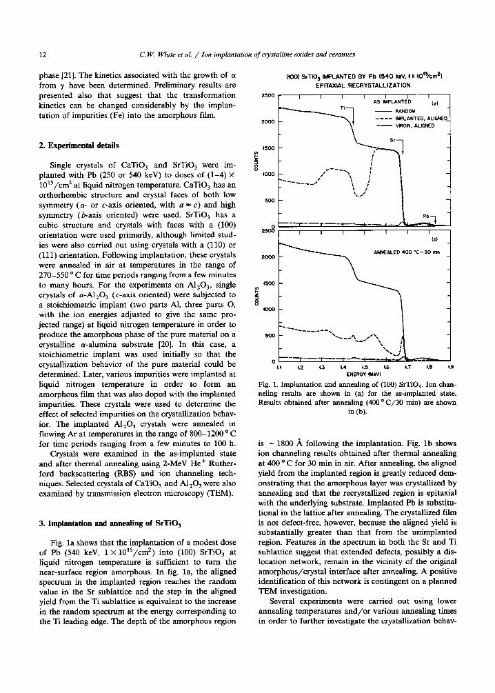
Fig. la shows that the implantation of a modest dose of Pb (540 keV, 1 X lO”/cm’) into (100) SrTiO, at liquid nitrogen temperature is sufficient to turn the near-surface region amorphous. In fig. la, the aligned spectrum in the implanted region reaches the random value in the Sr sublattice and the step in the aligned yield from the Ti sublattice is equivalent to the increase in the random spectrum at the energy corresponding to the Ti leading edge. The depth of the amorphous region
(KIO) SrTD3 IMPLANTED BY Pb (540 keV, IX ~O’%X?)
EPITAXIAL RECRYSTALLIZATION
Sr kl : :
I”----\ : ----___/’
\ \ : \ \ 1’ \ ..’
I I I I I I I
lb1
AWEALED 400 T-30 mn 2OQO
Fig. 1. Implantation and annealing of (100) SrTiO,. Ion chan- neling results are shown in (a) for the as-implanted state. Results obtained after annealing (400°C/30 min) are shown
in (b).
is - 1800 A following the implantation. Fig. lb shows ion channeling results obtained after thermal annealing at 400 o C for 30 min in air. After annealing, the aligned yield from the implanted region is greatly reduced dem- onstrating that the amorphous layer was crystallized by annealing and that the recrystallized region is epitaxial with the underlying substrate. Implanted Pb is substitu- tional in the lattice after annealing. The crystallized film is not defect-free, however, because the aligned yield is substantially greater than that from the unimplanted region. Features in the spectrum in both the Sr and Ti sublattice suggest that extended defects, possibly a dis- location network, remain in the vicinity of the original amorphous/crystal interface after annealing. A positive identification of this network is contingent on a planned TEM investigation.
Several experiments were carried out using lower annealing temperatures and/or various annealing times in order to further investigate the crystallization behav-
C. W. White et al. / Ion implantation of crystalline oxldes and ceramics 13
RECRYSTALLIZATION OF Pb (540 keV, 4 x ~O’%xn*) IMPLANTED (100) SrTi03
500 - RAWM
---- AS IMPLANTED -- ANNEALED 302 *C/45 mm
1
d
t.t 4.2 L3 4.4 4.5 1.6 L7 19 (9
ENERGY (MeVI
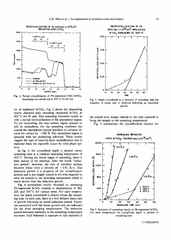
Fig. 2. Partial crystallization of Pb-implanted (100) SrTiO,. Annealing was carried out at 302 o C for 45 min.
ior of implanted SrTiO,. Fig. 2 shows the channeling results obtained after annealing implanted SrTiO, at 302°C for 45 min. This annealing treatment results in only a partial recrystallization of the amorphous region. To ion channeling, the near-surface region appears to still be amorphous, but the annealing treatment has caused the amorphous/crystal interface to advance to- ward the surface by - 800 A. The crystallized region is epitaxial with the underlying substrate. These results suggest the type of layer-by-layer crystallization that is expected when the regrowth occurs by solid-phase epi- taxy.
In fig. 3, the crystallized depth is plotted versus annealing time at a constant annealing temperature of 302°C. During the initial stages of annealing, there is little motion of the interface. After the initial “induc- tion period”, however, the rate of interface motion becomes linear with a velocity of - 0.91 A/s. This induction period is a property of the crystallization process and is not simply related to the time required to raise the sample to the annealing temperature which is much shorter than the induction period.
Fig. 4 summarizes results obtained by annealing Pb-implanted SrTiO, crystals at temperatures of 302, 325, and 350 o C for various times. For each tempera- ture, the depth crystallized is plotted versus the anneal- ing time. In each case, there is a well defined linear rate of growth following an initial induction period. Veloci- ties associated with this linear growth rate are indicated for the three annealing temperatures. The induction period decreases markedly as the annealing temperature increases. Such behavior is opposite to that expected if
RECRYSTALLIZATION OF Pb
(540 krV, IX ~O’S/ctn2, IMPLANTED
SrTi03 ANNEALING AT 302 =X
I I I I I I
0 10 20 30 40 50 60 TIME
Fig. 3. Depth crystallized as a function of annealing time (in minutes). A linear rate is observed following an induction
period.
the period were simply related to the time required to bring the sample to the annealing temperature.
Fig. 5 summarizes the crystallization kinetics for
ANNEALING BEHAVIOR
((00) SrTi03- Pb(540 keV,~rt0’%m2)
0
I I I I I
0 10 20 30 40 50 60
ANNEALING TIME (mn)
Fig. 4. Summary of annealing results of Pb-implanted SrTiO,. For each temperature the crystallized depth is plotted vs
annealing time.
I. CERAMICS
14 C. W. White et al. / Ion implantation of crystalhe oxrdes and ceramics
CRYSTALLIZATION OF AMORPHOUS SrT103
AMORPHOUS --c CRYSTAL TRANSFORMATION
T(‘C)
350 325 300 275
0.1 I I I I I I I I.55 1.65 4.75 4.65
+ xf03(“K-‘)
Fig. 5. Kinetics of crystallization of Pb-implanted (100) SrTiO,. Growth velocities are the linear rates measured following an
induction period at each temperature.
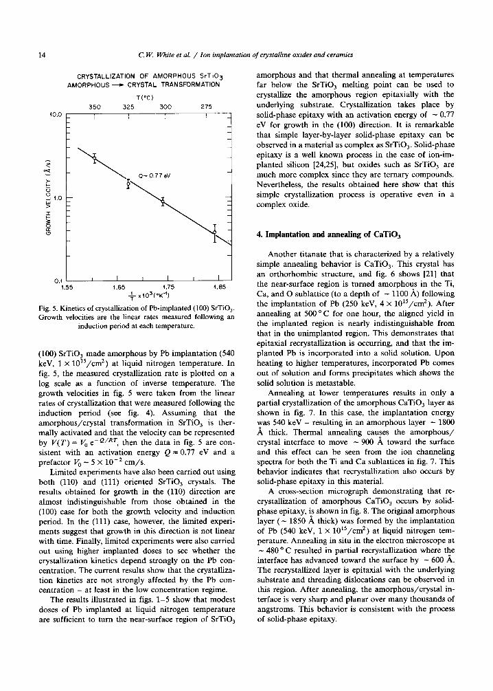
(100) SrTiO, made amorphous by Pb implantation (540 keV, 1 x 10r5/cm2) at liquid nitrogen temperature. In fig. 5, the measured crystallization rate is plotted on a log scale as a function of inverse temperature. The growth velocities in fig. 5 were taken from the linear rates of crystallization that were measured following the induction period (see fig. 4). Assuming that the amorphous/crystal transformation in SrTiO, is ther- mally activated and that the velocity can be represented by V(T) = V, e- QiRT, then the data in fig. 5 are con- sistent with an activation energy Q = 0.77 eV and a prefactor V0 - 5 X lo-* cm/s.
Limited experiments have also been carried out using both (110) and (111) oriented SrTiO, crystals. The results obtained for growth in the (110) direction are almost indistinguishable from those obtained in the (100) case for both the growth velocity and induction period. In the (111) case, however, the limited experi- ments suggest that growth in this direction is not linear with time. Finally, limited experiments were also carried out using higher implanted doses to see whether the crystallization kinetics depend strongly on the Pb con- centration. The current results show that the crystalliza- tion kinetics are not strongly affected by the Pb con- centration - at least in the low concentration regime.
The results illustrated in figs. l-5 show that modest doses of Pb implanted at liquid nitrogen temperature are sufficient to turn the near-surface region of SrTiO,
amorphous and that thermal annealing at temperatures far below the SrTiO, melting point can be used to crystallize the amorphous region epitaxially with the underlying substrate. Crystallization takes place by solid-phase epitaxy with an activation energy of - 0.77 eV for growth in the (100) direction. It is remarkable that simple layer-by-layer solid-phase epitaxy can be observed in a material as complex as SrTiO,. Solid-phase epitaxy is a well known process in the case of ion-im- planted silicon [24,25], but oxides such as SrTiO, are much more complex since they are ternary compounds. Nevertheless, the results obtained here show that this simple crystallization process is operative even in a complex oxide.
4. Implantation and annealing of CaTiOs
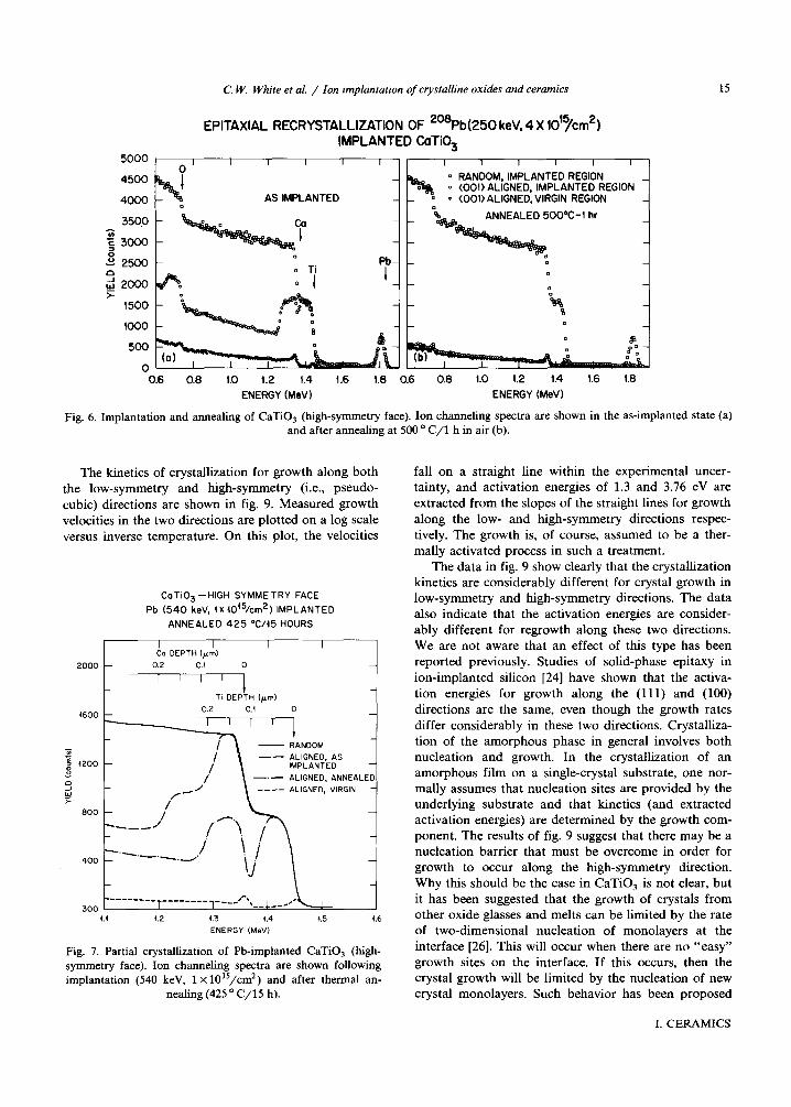
Another titanate that is characterized by a relatively simple annealing behavior is CaTiO,. This crystal has an orthorhombic structure, and fig. 6 shows [21] that the near-surface region is turned amorphous in the Ti, Ca, and 0 sublattice (to a depth of - 1100 A) following the implantation of Pb (250 keV, 4 x 10¹⁵/cm2). After annealing at 500°C for one hour, the aligned yield in the implanted region is nearly indistinguishable from that in the unimplanted region. This demonstrates that epitaxial recrystallization is occurring, and that the im- planted Pb is incorporated into a solid solution. Upon heating to higher temperatures, incorporated Pb comes out of solution and forms precipitates which shows the solid solution is metastable.
Annealing at lower temperatures results in only a partial crystallization of the amorphous CaTiO, layer as shown in fig. 7. In this case, the implantation energy was 540 keV - resulting in an amorphous layer - 1800 A thick. Thermal annealing causes the amorphous/ crystal interface to move - 900 A toward the surface and this effect can be seen from the ion channeling spectra for both the Ti and Ca sublattices in fig. 7. This behavior indicates that recrystallization also occurs by solid-phase epitaxy in this material.
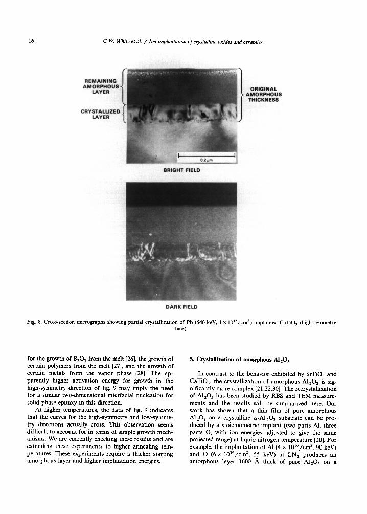
A cross-section micrograph demonstrating that re- crystallization of amorphous CaTiO, occurs by solid- phase epitaxy, is shown in fig. 8. The original amorphous layer (- 1850 A thick) was formed by the implantation of Pb (540 keV, 1 X 10’5/cm2) at liquid nitrogen tem- perature. Annealing in situ in the electron microscope at - 480 o C resulted in partial recrystallization where the interface has advanced toward the surface by - 600 A. The recrystallized layer is epitaxial with the underlying substrate and threading dislocations can be observed in this region. After annealing, the amorphous/crystal in- terface is very sharp and planar over many thousands of angstroms. This behavior is consistent with the process of solid-phase epitaxy.
AS IMPLANTED
3500 ? E 3000 a
2 2500 D p 2000
I500
0.6 0.8 t.0 1.2 I.4 1.6 1.8 0.6 0.8 I.0 1.2 1.4 1.6 1.8
ENERGY b&V) ENERGY @VW’)
C. W. White et al. / Ion implantation of crystalline oxides and ceramics
EPITAXIAL RECRYSTALLIZATION OF 208Pb(250 keV, 4 X 10’5/Crn2) IMPLANTED CaTiO,
15
Fig. 6. Implantation and annealing of CaTiOs (high-symmetry face). Ion channeling spectra are shown in the as-implanted state (a) and after annealing at 500 o C/l h in air (b).
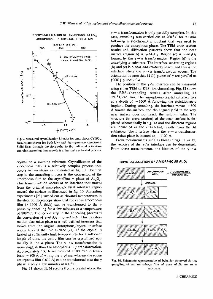
The kinetics of crystallization for growth along both the low-symmetry and high-symmetry (i.e., pseudo- cubic) directions are shown in fig. 9. Measured growth velocities in the two directions are plotted on a log scale versus inverse temperature. On this plot, the velocities
CaTi03 -HIGH SYMMETRY FACE
Pb (540 keV, 4 x ~0’5/cm2) IMPLANTED
ANNEALED 425 OC/i5 HOURS
2000
1600 I “1 0 I
\
-- ALIGNED, AS IMPLANTED
-‘- ALIGNED,
./ ---- ALIGNED, VIRGIN
3nn ___ 1.1 4.2 4.3 4.4 4.5 +.6
ENERGY It&V)
Fig. 7. Partial crystallization of Pb-implanted CaTiO, (high- symmetry face). Ion channeling spectra are shown following implantation (540 keV, 1 x 10i5/cm2) and after thermal an-
nealing (425 o C/15 h).
fall on a straight line within the experimental uncer- tainty, and activation energies of 1.3 and 3.76 eV are extracted from the slopes of the straight lines for growth along the low- and high-symmetry directions respec- tively. The growth is, of course, assumed to be a ther- mally activated process in such a treatment.
The data in fig. 9 show clearly that the crystallization kinetics are considerably different for crystal growth in low-symmetry and high-symmetry directions. The data also indicate that the activation energies are consider- ably different for regrowth along these two directions. We are not aware that an effect of this type has been reported previously. Studies of solid-phase epitaxy in ion-implanted silicon [24] have shown that the activa- tion energies for growth along the (111) and (100) directions are the same, even though the growth rates differ considerably in these two directions. Crystalliza- tion of the amorphous phase in general involves both nucleation and growth. In the crystallization of an amorphous film on a single-crystal substrate, one nor- mally assumes that nucleation sites are provided by the underlying substrate and that kinetics (and extracted activation energies) are determined by the growth com- ponent. The results of fig. 9 suggest that there may be a nucleation barrier that must be overcome in order for growth to occur along the high-symmetry direction. Why this should be the case in CaTiO, is not clear, but it has been suggested that the growth of crystals from other oxide glasses and melts can be limited by the rate of two-dimensional nucleation of monolayers at the interface [26]. This will occur when there are no “easy” growth sites on the interface. If this occurs, then the crystal growth will be limited by the nucleation of new crystal monolayers. Such behavior has been proposed
I. CERAMICS
16 C. W. White et al. / Ion implantation of cytalline oxides and ceramics
DARK FIELD
Fig. 8. Cross-section micrographs showing partial crystallization of Pb (540 keV, 1 X 10’5/cm2) implanted CaTiO, (high-symmetry face).
for the growth of B,O, from the melt [26], the growth of certain polymers from the melt [27], and the growth of certain metals from the vapor phase [28]. The ap- parently higher activation energy for growth in the high-symmetry direction of fig. 9 may imply the need for a similar two-dimensional interfacial nucleation for solid-phase epitaxy in this direction.
At higher temperatures, the data of fig. 9 indicates that the curves for the high-symmetry and low-symme- try directions actually cross. This observation seems difficult to account for in terms of simple growth mech- anisms. We are currently checking these results and are extending these experiments to higher annealing tem- peratures. These experiments require a thicker starting amorphous layer and higher implantation energies.
5. Crystallization of amorphous Al24
In contrast to the behavior exhibited by SrTiO, and CaTiO,, the crystallization of amorphous Al,O, is sig- nificantly more complex [21,22,30]. The recrystallization of Al,O, has been studied by RBS and TEM measure- ments and the results will be summarized here. Our work has shown that a thin film of pure amorphous Al,O, on a crystalline cy-Al,O, substrate can be pro- duced by a stoichiometric implant (two parts Al, three parts 0, with ion energies adjusted to give the same projected range) at liquid nitrogen temperature [20]. For example, the implantation of Al (4 x 10’6/cm2, 90 keV) and 0 (6 X 10¹⁶/cm2, 55 keV) at LN, produces an amorphous layer 1600 A thick of pure Al,O, on a
C. W. White et al. / Ion wnplantatron of crystalhne oxldes and ceramics 17
RECRYSTALLIZATION OF AMORPHOUS CaTi
AMORPHOUS - CRYSTAL TRANSITION
TEMPERATURE (“C)
500 450 400
I I I 0 LOW SYMMETRY FACE -
0 HIGH SYMMETRY FACE -
kO-’ 4.3 1.4 1.5
$ (OK-‘) X IO3
Fig. 9. Measured crystallization kinetics for amorphous CaTiO,. Results are shown for both low- and high-symmetry directions. Solid lines through the data refer to the indicated activation energies, assuming that growth is a thermally activated process.
crystalline a alumina substrate. Crystallization of the amorphous film is a relatively complex process that occurs in two stages as illustrated in fig. 10. The first step in the annealing process is the conversion of the amorphous film to the crystalline y phase of Al,O,. This transformation occurs at an interface that moves from the original amorphous/crystal interface region toward the surface as illustrated in fig. 10. Annealing experiments [29] carried out at elevated temperatures in the electron microscope show that the entire amorphous film (- 1600 A thick) can be transformed to the y phase by annealing for a few minutes at a temperature of 800°C. The second step in the annealing process is the conversion of y-Al,O, into a-Alz03. This transfor- mation also takes place at a well-defined interface that moves from the original amorphous/crystal interface region toward the free surface [21]. If the crystal is heated at sufficiently high temperatures for a sufficient length of time, the entire film can be crystallized epi- taxially in the a phase. The y -+ a transformation is more sluggish than the amorphous + y transformation. Approximately 100 h are required at 800°C to trans- form - 800 A of y into the a phase, whereas the entire amorphous film (1600 A) can be transformed into the y phase in only a few minutes at 800 ’ C.
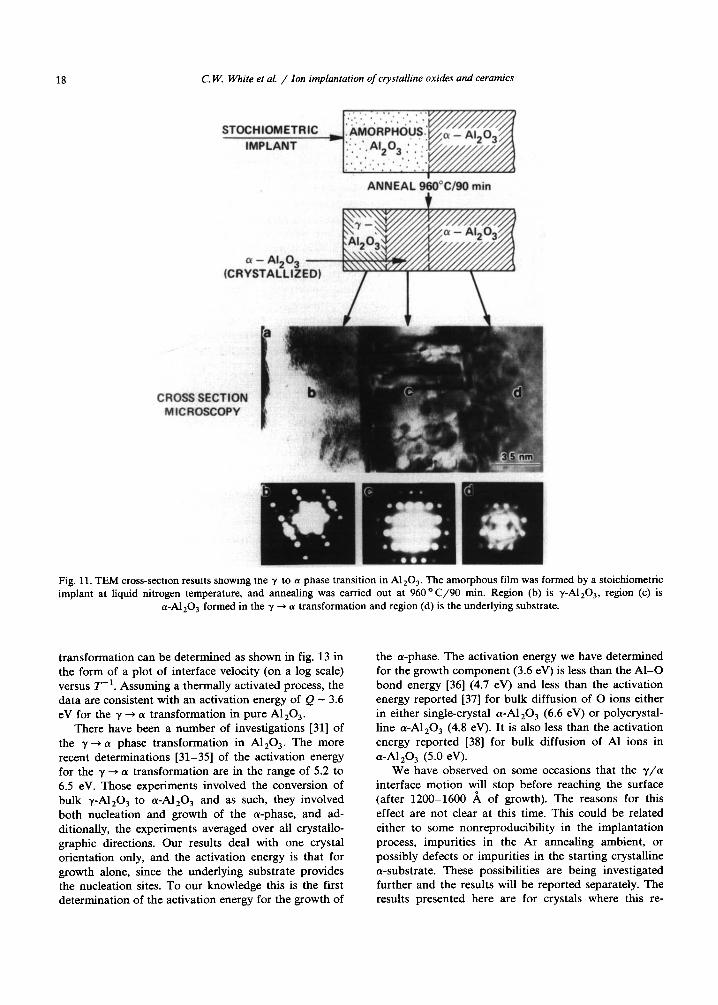
Fig. 11 shows TEM results from a crystal where the
y -+ a transformation is only partially complete. In this case, annealing was carried out at 96O’C for 90 min following a stoichiometric implant that was used to produce the amorphous phase. The TEM cross-section results and diffraction patterns show that the near surface (region b) is y-A120,. Region (c) is a-Al,O, formed by the y + LY transformation. Region (d) is the underlying a-substrate. The interface separating regions (b) and (c) is planar and relatively sharp, and this is the interface where the y + a transformation occurs. The orientation is such that (111) planes of y are parallel to (0001) planes of a.
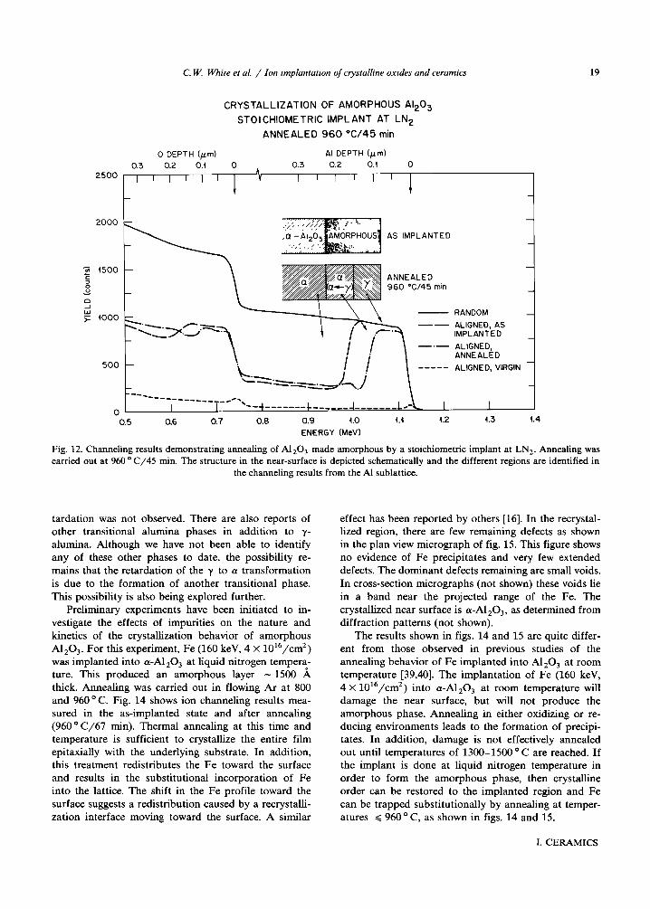
The position of the y/a interface can be measured using either TEM or RBS-ion channeling. Fig. 12 shows the RBS-channeling results after annealing at 950°C/45 min. The amorphous/crystal interface lies at a depth of - 1600 A following the stoichiometric implant. During annealing, the interface moves - 500 A toward the surface, and the aligned yield in the very near surface does not reach the random value. The structure (in cross section) of the near surface is de- picted schematically in fig. 12 and the different regions are identified in the channeling results from the Al sublattice. The interface where the y + a transforma- tion takes place is located at - 1100 A.
From measurements such as those in figs. 11 or 12, the velocity of the y/a interface can be determined. From these measurements, the kinetics of the y + a
CRYSTALLIZATION OF AMORPHOUS AI,01
STOCHIOMETRIC
IMPLANT-LN,
1 ANNEAL
Fig. 10. Schematic representation of behavior observed during annealing of an amorphous film of pure Al,O, on an a
substrate.
I. CERAMICS
C. W. Whiie et al. / Ion implantation of crystalline oxides and ceramics
Fig. 11. TEM cross-sectron resuns snowmg tne y to (x phase transition in Al,O,. The amorphous film was formed by a stoichiometric implant at liquid nitrogen temperature, and annealing was carried out at 960 o C/90 min. Region (b) is y-Al,O,, region (c) is
(~-Alr0~ formed in the y + a transformation and region (d) is the underlying substrate.
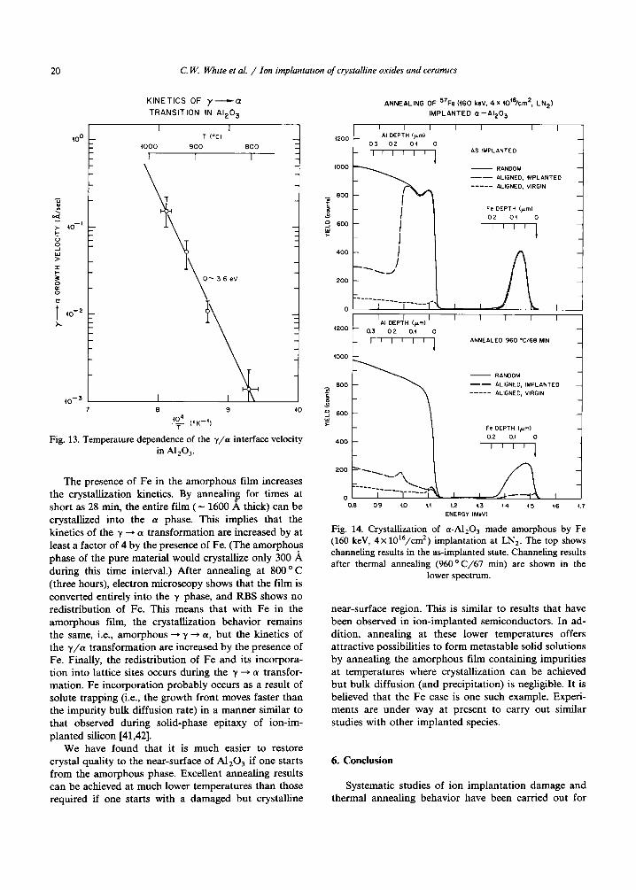
transformation can be determined as shown in fig. 13 in the form of a plot of interface velocity (on a log scale) versus T-‘. Assuming a thermally activated process, the data are consistent with an activation energy of Q - 3.6 eV for the y + (Y transformation in pure Al,O,.
There have been a number of investigations [31] of the y -+ (Y phase transformation in Al,O,. The more recent determinations [31-351 of the activation energy for the y + (Y transformation are in the range of 5.2 to 6.5 eV. Those experiments involved the conversion of bulk y-Al,O, to a-A1203 and as such, they involved both nucleation and growth of the a-phase, and ad- ditionally, the experiments averaged over all crystallo- graphic directions. Our results deal with one crystal orientation only, and the activation energy is that for growth alone, since the underlying substrate provides the nucleation sites. To our knowledge this is the first determination of the activation energy for the growth of
the o-phase. The activation energy we have determined for the growth component (3.6 ev) is less than the Al-O bond energy [36] (4.7 eV) and less than the activation energy reported [37] for bulk diffusion of 0 ions either in either single-crystal cu-Al,O, (6.6 eV) or polycrystal- line a-Al,O, (4.8 ev). It is also less than the activation energy reported [38] for bulk diffusion of Al ions in a-A1203 (5.0 eV).
We have observed on some occasions that the u/a: interface motion will stop before reaching the surface (after 1200-1600 A of growth). The reasons for this effect are not clear at this time. This could be related either to some nonreproducibility in the implantation process, impurities in the Ar annealing ambient, or possibly defects or impurities in the starting crystalline a-substrate. These possibilities are being investigated further and the results will be reported separately. The results presented here are for crystals where this re-
C. W. White et al. / Ion rmplantatron of crystalline oxrdes and ceramics
CRYSTALLIZATION OF AMORPHOUS A&O3 STOICHIOMETRIC IMPLANT AT LN2
ANNEALED 960 “C/45 min
0 DEPTH (pm) Al DEPTH (pm)
0.3 0.2 0.1 0 0.3 0.2 0.4 0
11’1’1’1 V I 1 I ’ I ’ 1
AS IMPLANTED
ANNEALED 960 ‘C/45 min
- RANDOM -I y 4000 ALIGNED, AS IMPLANTED
-.- ALIGNED, ANNEALED
500 ----- ALIGNED, VIRGIN
”
0.5 0.6 0.7 0.0 0.9 1.0 1.4 i.2
ENERGY (t&V)
4.3 4.4
19
Fig. 12. Channeling results demonstrating annealing of Al 203 made amorphous by a stoichiometric implant at LN,. Annealing was
carried out at 960 o C/45 min. The structure in the near-surface is depicted schematically and the different regions are identified in
the channeling results from the Al sublattice.
tardation was not observed. There are also reports of other transitional alumina phases in addition to y- alumina. Although we have not been able to identify any of these other phases to date, the possibility re- mains that the retardation of the y to (Y transformation is due to the formation of another transitional phase. This possibility is also being explored further.
Preliminary experiments have been initiated to in- vestigate the effects of impurities on the nature and kinetics of the crystallization behavior of amorphous Al,O,. For this experiment, Fe (160 keV, 4 x 10’6/cm2) was implanted into c~-Al,O, at liquid nitrogen tempera- ture. This produced an amorphous layer - 1500 A thick. Annealing was carried out in flowing Ar at 800 and 96O’C. Fig. 14 shows ion channeling results mea- sured in the as-implanted state and after annealing (960 o C/67 min). Thermal annealing at this time and temperature is sufficient to crystallize the entire film epitaxially with the underlying substrate. In addition, this treatment redistributes the Fe toward the surface and results in the substitutional incorporation of Fe into the lattice. The shift in the Fe profile toward the surface suggests a redistribution caused by a recrystalli- zation interface moving toward the surface. A similar
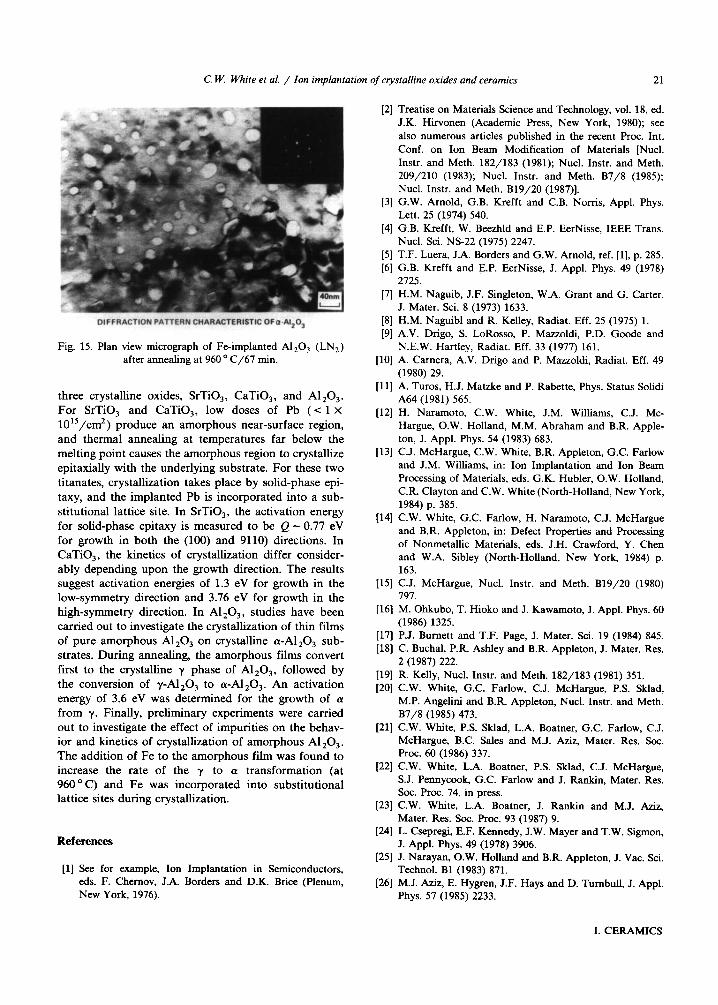
effect has been reported by others [16]. In the recrystal- lized region, there are few remaining defects as shown in the plan view micrograph of fig. 15. This figure shows no evidence of Fe precipitates and very few extended defects. The dominant defects remaining are small voids. In cross-section micrographs (not shown) these voids lie in a band near the projected range of the Fe. The crystallized near surface is cr-Al,O,, as determined from diffraction patterns (not shown).
The results shown in figs. 14 and 15 are quite differ- ent from those observed in previous studies of the annealing behavior of Fe implanted into Al *03 at room temperature [39,40]. The implantation of Fe (160 keV, 4 X 10r6/cm2) into o-Al,O, at room temperature will damage the near surface, but will not produce the amorphous phase. Annealing in either oxidizing or re- ducing environments leads to the formation of precipi- tates. In addition, damage is not effectively annealed out until temperatures of 1300-1500 o C are reached. If the implant is done at liquid nitrogen temperature in order to form the amorphous phase, then crystalline order can be restored to the implanted region and Fe can be trapped substitutionally by annealing at temper- atures Q 960°C, as shown in figs, 14 and 15.
I. CERAMICS
20 C. W. White et al. / Ion implantation of crystalline oxides and ceramws
KINETICS OF y-a ANNEALING OF “Fe 060 keV, 4 X ~O’6/,rt2, LN2)
TRANSITION IN AI,O, IMPLANTED o -A1203
I I I I I I I I I I I I 1 T (“Cl
(000 900 800
1 I I
40-3 L I I I\ 7 a 9 10
!g (OK-Q
Fig. 13. Temperature dependence of the y/a interface velocity in Al,O,.
The presence of Fe in the amorphous film increases the crystallization kinetics. By annealing for times at short as 28 min, the entire film (- 1600 A thick) can be crystallized into the a phase. This implies that the kinetics of the y + a transformation are increased by at least a factor of 4 by the presence of Fe. (The amorphous phase of the pure material would crystallize only 300 A during this time interval.) After annealing at 800°C (three hours), electron microscopy shows that the film is converted entirely into the y phase, and RBS shows no redistribution of Fe. This means that with Fe in the amorphous film, the crystallization behavior remains the same, i.e., amorphous + y + a, but the kinetics of the y/a transformation are increased by the presence of Fe. Finally, the redistribution of Fe and its incorpora- tion into lattice sites occurs during the y + a transfor- mation. Fe incorporation probably occurs as a result of solute trapping (i.e., the growth front moves faster than the impurity bulk diffusion rate) in a manner similar to that observed during solid-phase epitaxy of ion-im- planted silicon [41,42].
We have found that it is much easier to restore crystal quality to the near-surface of Al,O, if one starts from the amorphous phase. Excellent annealing results can be achieved at much lower temperatures than those required if one starts with a damaged but crystalline
Fe DEPTH (pm1
++i
0 I
I I AI DEPTH (pm1
I I I I I I
‘2oo - 0.3 02 0.4 0
1000
ANNEALED 960 T/58 MN
- RANDOM
-- ALIGNED. IMPLANTED ----- ALIGNED. VIRGIN
Fc DEPTH Qml
0.2 0.4 0
I 1 I 1
I
-0.0 09 4.0 4.4 1.2 4.3 (4 45 (6 4.7 ENERGY (Me”)
Fig. 14. Crystallization of a-Al,O, made amorphous by Fe (160 keV, 4~1O’~/crn’) implantation at LN,. The top shows channeling results in the as-implanted state. Channeling results after thermal annealing (960 o C/67 min) are shown in the
lower spectrum.
near-surface region. This is similar to results that have been observed in ion-implanted semiconductors. In ad- dition, annealing at these lower temperatures offers attractive possibilities to form metastable solid solutions by annealing the amorphous film containing impurities at temperatures where crystallization can be achieved but bulk diffusion (and precipitation) is negligible. It is believed that the Fe case is one such example. Experi- ments are under way at present to carry out similar studies with other implanted species.
6. Conclusion
Systematic studies of ion implantation damage and thermal annealing behavior have been carried out for
C. W. White et al. / Ion implantation of crystalline oxides and ceramics 21
Fig. 15. Plan view micrograph of Fe-implanted Al,O, (LN,) after annealing at 960 ’ C/67 min.
three crystalline oxides, SrTiO,, CaTiO,, and Al 203. For SrTiO, and CaTiO,, low doses of Pb (< 1 x
10i5/cm2) produce an amorphous near-surface region, and thermal annealing at temperatures far below the melting point causes the amorphous region to crystallize epitaxially with the underlying substrate. For these two titanates, crystallization takes place by solid-phase epi- taxy, and the implanted Pb is incorporated into a sub- stitutional lattice site. In SrTiO,, the activation energy for solid-phase epitaxy is measured to be Q - 0.77 eV for growth in both the (100) and 9110) directions. In CaTiO,, the kinetics of crystallization differ consider- ably depending upon the growth direction. The results suggest activation energies of 1.3 eV for growth in the low-symmetry direction and 3.76 eV for growth in the high-symmetry direction. In Al,O,, studies have been carried out to investigate the crystallization of thin films of pure amorphous Al,O, on crystalline a-Al,O, sub- strates. During annealing, the amorphous films convert first to the crystalline y phase of Al,O,, followed by the conversion of y-Al,O, to a-Al,O,. An activation energy of 3.6 eV was determined for the growth of a! from y. Finally, preliminary experiments were carried out to investigate the effect of impurities on the behav- ior and kinetics of crystallization of amorphous Al,O,. The addition of Fe to the amorphous film was found to increase the rate of the y to a transformation (at 960°C) and Fe was incorporated into substitutional lattice sites during crystallization.
References
[l] See for example, Ion Implantation in Semiconductors,
eds. F. Chemov, J.A. Borders and D.K. Brice (Plenum,
New York, 1976).
PI
131
141
[51
WI
[71
PI
[91
WI
1111
WI
1131
1141
1151
WI
[I71
WI
1191
PO1
WI
WI
1231
v41
v51
WI
Treatise on Materials Science and Technology, vol. 18, ed.
J.K. Hirvonen (Academic Press, New York, 1980); see
also numerous articles published in the recent Proc. Int.
Conf. on Ion Beam Modification of Materials [Nucl.
Instr. and Meth. 182/183 (1981); Nucl. Instr. and Meth.
209/210 (1983); Nucl. Instr. and Meth. B7/8 (1985);
Nucl. Instr. and Meth. B19/20 (1987)].
G.W. Arnold, G.B. Krefft and C.B. Norris, Appl. Phys.
Lett. 25 (1974) 540.
G.B. Krefft, W. Beezhld and E.P. EerNisse, IEEE Trans.
Nucl. Sci. NS-22 (1975) 2247.
T.F. Luera, J.A. Borders and G.W. Arnold, ref. [l], p. 285.
G.B. Krefft and E.P. EerNisse, J. Appl. Phys. 49 (1978) 2725.
H.M. Naguib, J.F. Singleton, W.A. Grant and G. Carter,
J. Mater. Sci. 8 (1973) 1633.
H.M. Naguibl and R. Kelley, Radiat. Eff. 25 (1975) 1.
A.V. Drigo, S. LoRosso, P. Mazzoldi, P.D. Goode and
N.E.W. Hartley, Radiat. Eff. 33 (1977) 161.
A. Camera, A.V. Drigo and P. Mazzoldi, Radiat. Eff. 49
(1980) 29.
A. Turos, H.J. Matzke and P. Rabette, Phys. Status Solidi A64 (1981) 565.
H. Naramoto, C.W. White, J.M. Williams, C.J. Mc-
Hargue, O.W. Holland, M.M. Abraham and B.R. Apple-
ton, J. Appl. Phys. 54 (1983) 683.
C.J. McHargue, C.W. White, B.R. Appleton, G.C. Farlow
and J.M. Williams, in: Ion Implantation and Ion Beam
Processing of Materials, eds. G.K. Hubler, O.W. Holland,
C.R. Clayton and C.W. White (North-Holland, New York,
1984) p. 385.
C.W. White, G.C. Farlow, H. Naramoto, C.J. McHargue
and B.R. Appleton, in: Defect Properties and Processing
of Nonmetallic Materials, eds. J.H. Crawford, Y. Chen
and W.A. Sibley (North-Holland, New York, 1984) p. 163.
C.J. McHargue, Nucl. Instr. and Meth. B19/20 (1980) 797.
M. Ohkubo, T. Hioko and J. Kawamoto, J. Appl. Phys. 60
(1986) 1325.
P.J. Burnett and T.F. Page, J. Mater. Sci. 19 (1984) 845.
C. Buchal, P.R. Ashley and B.R. Appleton, J. Mater. Res.
2 (1987) 222.
R. Kelly, Nucl. Instr. and Meth. 182/183 (1981) 351.
C.W. White, G.C. Farlow, C.J. McHargue, P.S. Sklad,
M.P. Angelini and B.R. Appleton, Nucl. Instr. and Meth.
B7/8 (1985) 473.
C.W. White, P.S. Sklad, L.A. Boatner, G.C. Farlow, C.J. McHargue, B.C. Sales and M.J. AZ&, Mater. Res. Sot.
Proc. 60 (1986) 337.
C.W. White, L.A. Boatner, P.S. Sklad, C.J. McHargue,
S.J. Pennycook, G.C. Farlow and J. Rankin, Mater. Res. Sot. Proc. 74, in press.
C.W. White, L.A. Boatner, J. Rankin and M.J. Aziz, Mater. Res. Sot. Proc. 93 (1987) 9.
L. Csepregi, E.F. Kennedy, J.W. Mayer and T.W. Sigmon, J. Appl. Phys. 49 (1978) 3906.
J. Narayan, O.W. Holland and B.R. Appleton, J. Vat. Sci. Technol. Bl (1983) 871.
M.J. Aziz, E. Hygren, J.F. Hays and D. Tumbull, J. Appl.
Phys. 57 (1985) 2233.
I. CERAMICS
22 C. W. White et al. / Ion implantation of crystalline oxides and ceramics
[27] J.D. Hoffman, G.T. Davis and J.I. Lauritzen, Jr., in:
Treatise on Solid State Chemistry, vol. 3, ed. N.B. Hannay (Plenum, New York, 1976) p. 541.
[28] J.P. Hirth and G.M. Pund, Progress in Materials Science,
vol. 11, ed. B. Chalmers (Pergamon, New York, 1963) p.
87. [29] P.S. Sklad, private communication.
[30] G.C. Farlow, P.S. Sklad, C.W. White, C.J. McHargue and
B.R. Appleton, Mater. Res. Sot. Proc. 60 (1986) 387.
[31] For a summary of some of the previous experiments, see
D.S. Tucker and J.J. Hren, Mater. Res. Sot. Proc. 31
(1984) 337.
[32] H. Schaper and L.L. Van Reijen, Thermochem. Acta 77
(1984) 383.
[33] S.J. Wilson and J.D. McConnell, J. Sol. Stat. Chem. 34
(1980) 315.
[34] B.E. Yoldas, Ceram. Bull. 54 (1975) 286.
[35] C.J.P. Steines, D.P.H. Hasselman and R.M. Spriggs, J. Am. Ceram. Sot. 54 (1971) 412.
[36] Handbook of Chemistry and Physics, 52nd ed. (Chem.
Rubber Co., Cleveland, Ohio, 1971) p. F-177.
[37] Y. Oishi and W.D. Kingery, J. Chem. Phys. 33 (1960) 480. [38] A.E. Paladin0 and W.D. Kingery, J. Chem. Phys. 37
(1962) 957.
[39] G.C. Farlow, C.W. White, C.J. McHargue, P.S. Sklad and
B.R. Appleton, Nucl. Instr. and Meth. B7/8 (1985) 541.
[40] C.J. McHargue, G.C. Farlow, P.S. SkIad, C.W. White, A.
Prez, N. Komilios and G. Marest, Nucl. Instr. and Meth.
B19/20 (1987) 813.
[41] S.U. Campisano, E. Rimini, P. Baeri and G. Foti, Appl.
Phys. Lett. 37 (1980) 170; S.U. Campisano, G. Foti, P.
Baeri, M.G. Grimaldi and E. Rimini, Appl. Phys. Lett. 37
(1980) 719.
[42] J.S. Williams and R.G. Elliman, Nucl. Instr. and Meth.
182/183 (1981) 289.