Embed Size (px)
Citation preview
Interrupts6
Section 6. Interrupts
HIGHLIGHTSThis section of the manual contains the following topics:
6.1 Introduction .................................................................................................................... 6-26.2 Non-Maskable Traps...................................................................................................... 6-66.3 Interrupt Processing Timing ......................................................................................... 6-116.4 Interrupt Control and Status Registers......................................................................... 6-146.5 Interrupt Setup Procedures.......................................................................................... 6-426.6 Register Map................................................................................................................6-436.7 Design Tips .................................................................................................................. 6-446.8 Related Application Notes............................................................................................ 6-456.9 Revision History ........................................................................................................... 6-46
© 2007 Microchip Technology Inc. DS70053D-page 6-1

dsPIC30F Family Reference Manual
6.1 IntroductionThe dsPIC30F interrupt controller module reduces the numerous peripheral interrupt requestsignals to a single interrupt request signal to the dsPIC30F CPU and has the following features:
• Up to 8 processor exceptions and software traps• 7 user selectable priority levels• Interrupt Vector Table (IVT) with up to 62 vectors• A unique vector for each interrupt or exception source• Fixed priority within a specified user priority level• Alternate Interrupt Vector Table (AIVT) for debug support• Fixed interrupt entry and return latencies
6.1.1 Interrupt Vector Table
The Interrupt Vector Table (IVT) is shown in Figure 6-1. The IVT resides in program memory,starting at location 0x000004. The IVT contains 62 vectors consisting of 8 non-maskable trapvectors plus up to 54 sources of interrupt. In general, each interrupt source has its own vector.Each interrupt vector contains a 24-bit wide address. The value programmed into each interruptvector location is the starting address of the associated Interrupt Service Routine (ISR).
6.1.2 Alternate Vector Table
The Alternate Interrupt Vector Table (AIVT) is located after the IVT as shown in Figure 6-1.Access to the AIVT is provided by the ALTIVT control bit (INTCON2<15>). If the ALTIVT bit isset, all interrupt and exception processes will use the alternate vectors instead of the defaultvectors. The alternate vectors are organized in the same manner as the default vectors.
The AIVT supports emulation and debugging efforts by providing a means to switch betweenan application and a support environment without requiring the interrupt vectors to bereprogrammed. This feature also enables switching between applications for evaluation ofdifferent software algorithms at run-time. If the AIVT is not needed, the AIVT should beprogrammed with the same addresses used in the IVT.
6.1.3 Reset Sequence
A device Reset is not a true exception because the interrupt controller is not involved in the Resetprocess. The dsPIC30F device clears its registers in response to a Reset which forces the PC tozero. The processor then begins program execution at location 0x000000. The user programsa GOTO instruction at the Reset address which redirects program execution to the appropriatestart-up routine.
Note: Any unimplemented or unused vector locations in the IVT and AIVT should beprogrammed with the address of a default interrupt handler routine that contains aRESET instruction.
DS70053D-page 6-2 © 2007 Microchip Technology Inc.

Section 6. InterruptsInterrupts
6
Figure 6-1: Interrupt Vector TableTable 6-1: Trap Vector Details
Dec
reas
ing
Nat
ural
Ord
er P
riorit
y
0x000000
0x000014
Reserved
Address Error Trap VectorStack Error Trap Vector
ReservedReservedReserved
Interrupt Vector 0Interrupt Vector 1
———
Interrupt Vector 52Interrupt Vector 53
Arithmetic Error Trap Vector
Oscillator Fail Trap Vector
ReservedInterrupt Vector 0Interrupt Vector 1
———
Interrupt Vector 52Interrupt Vector 53
IVT
AIVT
0x0000800x00007E
0x0000FE
ReservedReserved
Address Error Trap VectorStack Error Trap Vector
ReservedReserved
Arithmetic Error Trap Vector
Oscillator Fail Trap Vector
0x000094
Reset – GOTO InstructionReset – GOTO Address 0x000002
Reserved0x0000820x000084
0x000004
See Table 6-2
Vector details.for Interrupt
Vector Number IVT Address AIVT Address Trap Source
0 0x000004 0x000084 Reserved1 0x000006 0x000086 Oscillator Failure2 0x000008 0x000088 Address Error3 0x00000A 0x00008A Stack Error4 0x00000C 0x00008C Arithmetic Error5 0x00000E 0x00008E Reserved6 0x000010 0x000090 Reserved7 0x000012 0x000092 Reserved
© 2007 Microchip Technology Inc. DS70053D-page 6-3

dsPIC30F Family Reference Manual
Table 6-2: Interrupt Vector Details
Vector Number IVT Address AIVT Address Interrupt Source
8 0x000014 0x000094 INT0 – External Interrupt 09 0x000016 0x000096 IC1 – Input Compare 110 0x000018 0x000098 OC1 – Output Compare 111 0x00001A 0x00009A T1 – Timer 112 0x00001C 0x00009C IC2 – Input Capture 213 0x00001E 0x00009E OC2 – Output Compare 214 0x000020 0x0000A0 T2 – Timer 215 0x000022 0x0000A2 T3 – Timer 316 0x000024 0x0000A4 SPI1 17 0x000026 0x0000A6 U1RX – UART1 Receiver18 0x000028 0x0000A8 U1TX – UART1 Transmitter19 0x00002A 0x0000AA ADC – ADC Convert Done20 0x00002C 0x0000AC NVM – NVM Write Complete21 0x00002E 0x0000AE I2C™ Slave Operation – Message
Detect22 0x000030 0x0000B0 I2C Master Operation – Message
Event Complete23 0x000032 0x0000B2 Change Notice Interrupt24 0x000034 0x0000B4 INT1 – External Interrupt 125 0x000036 0x0000B6 IC7 – Input Capture 726 0x000038 0x0000B8 IC8 – Input Capture 827 0x00003A 0x0000BA OC3 – Output Compare 328 0x00003C 0x0000BC OC4 – Output Compare 429 0x00003E 0x0000BE T4 – Timer 430 0x000040 0x0000C0 T5 – Timer 531 0x000042 0x0000C2 INT2 – External Interrupt 232 0x000044 0x0000C4 U2RX – UART2 Receiver33 0x000046 0x0000C6 U2TX – UART2 Transmitter34 0x000048 0x0000C8 SPI2 35 0x00004A 0x0000CA CAN136 0x00004C 0x0000CC IC3 – Input Capture 337 0x00004E 0x0000CE IC4 – Input Capture 438 0x000050 0x0000D0 IC5 – Input Capture 539 0x000052 0x0000D2 IC6 – Input Capture 640 0x000054 0x0000D4 OC5 – Output Compare 541 0x000056 0x0000D6 OC6 – Output Compare 642 0x000058 0x0000D8 OC7 – Output Compare 743 0x00005A 0x0000DA OC8 – Output Compare 844 0x00005C 0x0000DC INT3 – External Interrupt 345 0x00005E 0x0000DE INT4 – External Interrupt 446 0x000060 0x0000E0 CAN2 47 0x000062 0x0000E2 PWM – PWM Period Match48 0x000064 0x0000E4 QEI – Position Counter Compare49 0x000066 0x0000E6 DCI – Codec Transfer Done50 0x000068 0x0000E8 LVD – Low Voltage Detect51 0x00006A 0x0000EA FLTA – MCPWM Fault A52 0x00006C 0x0000EC FLTB – MCPWM Fault B
53-61 0x00006E-0x00007E 0x00006E-0x00007E Reserved
DS70053D-page 6-4 © 2007 Microchip Technology Inc.

Section 6. InterruptsInterrupts
6
6.1.4 CPU Priority StatusThe CPU can operate at one the of sixteen priority levels, 0-15. An interrupt or trap source musthave a priority level greater than the current CPU priority in order to initiate an exception process.Peripheral and external interrupt sources can be programmed for level 0-7, while CPU prioritylevels 8-15 are reserved for trap sources. A trap is a non-maskable interrupt source intended todetect hardware and software problems (see Section 6.2 “Non-Maskable Traps”). The prioritylevel for each trap source is fixed and only one trap is assigned to a priority level. Note that aninterrupt source programmed to priority level 0 is effectively disabled, since it can never begreater than the CPU priority.The current CPU priority level is indicated by the following four status bits:
• IPL<2:0> status bits located in SR<7:5>• IPL3 status bit located in CORCON<3>
The IPL<2:0> status bits are readable and writable, so the user may modify these bits to disableall sources of interrupts below a given priority level. If IPL<2:0> = 3, for example, the CPU willnot be interrupted by any source with a programmed priority level of 0, 1, 2 or 3. Trap events have higher priority than any user interrupt source. When the IPL3 bit is set, a trapevent is in progress. The IPL3 bit can be cleared, but not set by the user. In some applications,it may be desirable to clear the IPL3 bit when a trap has occurred and branch to an instructionother than the instruction after the one that originally caused the trap to occur.All user interrupt sources can be disabled by setting IPL<2:0> = 111.
6.1.5 Interrupt Priority
Each peripheral interrupt source can be assigned to one of the seven priority levels. The userassignable interrupt priority control bits for each individual interrupt are located in the LeastSignificant 3 bits of each nibble within the IPCx register(s). Bit 3 of each nibble is not used andis read as a ‘0’. These bits define the priority level assigned to a particular interrupt. The usablepriority levels start at ‘1’ as the lowest priority and level 7 as the highest priority. If the IPC bitsassociated with an interrupt source are all cleared, then the interrupt source is effectivelydisabled.
Since more than one interrupt request source may be assigned to a specific priority level, anoption is provided to resolve priority conflicts within a given user-assigned level. Each source ofinterrupt has a natural order priority based on its location in the IVT. Table 6-2 shows the locationof each interrupt source in the IVT. The lower numbered interrupt vectors have higher naturalpriority, while the higher numbered vectors have lower natural priority. The overall priority levelfor any pending source of interrupt is determined first by the user-assigned priority of that sourcein the IPCx register, then by the natural order priority within the IVT.Natural order priority is used only to resolve conflicts between simultaneous pending interruptswith the same user-assigned priority level. Once the priority conflict is resolved and the exceptionprocess begins, the CPU can only be interrupted by a source with a higher user-assigned priority.Interrupts with the same user-assigned priority but a higher natural order priority, that becomepending after the exception process begins, will remain pending until the current exceptionprocess completes.The ability for the user to assign each interrupt source to one of seven priority levels means thatthe user can give an interrupt with a low natural order priority a very high overall priority level. Forexample: the PLVD (Programmable Low Voltage Detect) can be given a priority of 7 and the INT0(External Interrupt 0) may be assigned to priority level 1, thus giving it a very low effective priority.
Note: The IPL<2:0> bits become read only bits when interrupt nesting is disabled. SeeSection 6.2.4.2 “Interrupt Nesting” for more information.
Note: If the application program reconfigures the interrupt priority levels on the fly, it mustdisable the interrupts while doing so. Failure to disable interrupts can produceunexpected results.
Note: The peripherals and sources of interrupt available in the IVT will vary depending onthe specific dsPIC30F device. The sources of interrupt shown in this documentrepresent a comprehensive listing of all interrupt sources found on dsPIC30Fdevices. Refer to the specific device data sheet for further details.
© 2007 Microchip Technology Inc. DS70053D-page 6-5

dsPIC30F Family Reference Manual
6.2 Non-Maskable TrapsTraps can be considered as non-maskable, nestable interrupts which adhere to a fixed prioritystructure. Traps are intended to provide the user a means to correct erroneous operation duringdebug and when operating within the application. If the user does not intend to take correctiveaction in the event of a trap error condition, these vectors must be loaded with the address of asoftware routine that will reset the device. Otherwise, the trap vector is programmed with theaddress of a service routine that will correct the trap condition.
The dsPIC30F has the four implemented sources of non-maskable traps listed below:
• Oscillator Failure Trap• Stack Error Trap• Address Error Trap• Arithmetic Error Trap
Note that many of these trap conditions can only be detected when they happen. Consequently,the instruction that caused the trap is allowed to complete before exception processing begins.Therefore, the user may have to correct the action of the instruction that caused the trap.
Each trap source has a fixed priority as defined by its position in the IVT. An oscillator failure traphas the highest priority, while an arithmetic error trap has the lowest priority (see Figure 6-1). Inaddition, trap sources are classified into two distinct categories: ‘Hard’ traps and ‘Soft’ traps.
6.2.1 Soft Traps
The arithmetic error trap (priority level 11) and stack error trap (priority level 12) are categorizedas ‘soft’ trap sources. Soft traps can be treated like non-maskable sources of interrupt thatadhere to the priority assigned by their position in the IVT. Soft traps are processed like interruptsand require 2 cycles to be sampled and Acknowledged prior to exception processing. Therefore,additional instructions may be executed before a soft trap is Acknowledged.
6.2.1.1 Stack Error Trap (Soft Trap, Level 12)
The stack is initialized to 0x0800 during Reset. A stack error trap will be generated should thestack pointer address ever be less than 0x0800.
There is a Stack Limit register (SPLIM) associated with the stack pointer that is uninitialized atReset. The stack overflow check is not enabled until a word write to SPLIM occurs.
All Effective Addresses (EA) generated using W15 as a source or destination pointer arecompared against the value in SPLIM. Should the EA be greater than the contents of the SPLIMregister, then a stack error trap is generated. In addition, a stack error trap will be generatedshould the EA calculation wrap over the end of data space (0xFFFF).
A stack error can be detected in software by polling the STKERR status bit (INTCON1<2>). Toavoid re-entering the Trap Service Routine, the STKERR status flag must be cleared in softwareprior to returning from the trap with a RETFIE instruction.
DS70053D-page 6-6 © 2007 Microchip Technology Inc.

Section 6. InterruptsInterrupts
6
6.2.1.2 Arithmetic Error Trap (Soft Trap, Level 11)Any of the following events will cause an arithmetic error trap to be generated:
• Accumulator A Overflow • Accumulator B Overflow• Catastrophic Accumulator Overflow• Divide by Zero• Shift Accumulator (SFTAC) operation exceeding +/-16 bits
There are three enable bits in the INTCON1 register that enable the three types of accumulatoroverflow traps. The OVATE control bit (INTCON1<10>) is used to enable traps for anAccumulator A overflow event. The OVBTE control bit (INTCON1<9>) is used to enable traps foran Accumulator B overflow event. The COVTE control bit (INTCON1<8>) is used to enable trapsfor a catastrophic overflow of either accumulator.
An Accumulator A or Accumulator B overflow event is defined as a carry-out from bit 31. Notethat no accumulator overflow can occur if the 31-bit Saturation mode is enabled for theaccumulator. A catastrophic accumulator overflow is defined as a carry-out from bit 39 of eitheraccumulator. No catastrophic overflow can occur if accumulator saturation (31-bit or 39-bit) isenabled.
Divide-by-zero traps cannot be disabled. The divide-by-zero check is performed during the firstiteration of the REPEAT loop that executes the divide instruction.
Accumulator shift traps cannot be disabled. The SFTAC instruction can be used to shift theaccumulator by a literal value or a value in one of the W registers. If the shift value exceeds+/-16 bits, an arithmetic trap will be generated. The SFTAC instruction will execute, but the resultsof the shift will not be written to the target accumulator.
An arithmetic error trap can be detected in software by polling the MATHERR status bit(INTCON1<4>). To avoid re-entering the Trap Service Routine, the MATHERR status flag mustbe cleared in software prior to returning from the trap with a RETFIE instruction. Before theMATHERR status bit can be cleared, all conditions that caused the trap to occur must also becleared. If the trap was due to an accumulator overflow, the OA and OB status bits (SR<15:14>)must be cleared. The OA and OB status bits are read only, so the user software must perform adummy operation on the overflowed accumulator (such as adding ‘0’) that will cause thehardware to clear the OA or OB status bit.
6.2.2 Hard Traps
Hard traps include exceptions of priority level 13 through level 15, inclusive. The address error(level 13) and oscillator error (level 14) traps fall into this category.
Like soft traps, hard traps can also be viewed as non-maskable sources of interrupt. Thedifference between hard traps and soft traps is that hard traps force the CPU to stop codeexecution after the instruction causing the trap has completed. Normal program execution flowwill not resume until after the trap has been Acknowledged and processed.
6.2.2.1 Trap Priority and Hard Trap Conflicts
If a higher priority trap occurs while any lower priority trap is in progress, processing of the lowerpriority trap will be suspended and the higher priority trap will be Acknowledged and processed.The lower priority trap will remain pending until processing of the higher priority trap completes.
Each hard trap that occurs must be Acknowledged before code execution of any type maycontinue. If a lower priority hard trap occurs while a higher priority trap is pending, Acknowledged,or is being processed, a hard trap conflict will occur. The conflict occurs because the lowerpriority trap cannot be Acknowledged until processing for the higher priority trap completes.
The device is automatically reset in a hard trap conflict condition. The TRAPR status bit(RCON<15>) is set when the Reset occurs, so that the condition may be detected in software.
© 2007 Microchip Technology Inc. DS70053D-page 6-7

dsPIC30F Family Reference Manual
6.2.2.2 Oscillator Failure Trap (Hard Trap, Level 14)
An oscillator failure trap event will be generated for any of the following reasons:
• The Fail-Safe Clock Monitor (FSCM) is enabled and has detected a loss of the system clock source.
• A loss of PLL lock has been detected during normal operation using the PLL.• The FSCM is enabled and the PLL fails to achieve lock at a Power-On Reset (POR).
An oscillator failure trap event can be detected in software by polling the OSCFAIL status bit(INTCON1<1>), or the CF status bit (OSCCON<3>). To avoid re-entering the Trap ServiceRoutine, the OSCFAIL status flag must be cleared in software prior to returning from the trap witha RETFIE instruction.
For more information about the FSCM, refer to Section 7. “Oscillator” and Section24. “Device Configuration”.
6.2.2.3 Address Error Trap (Hard Trap, Level 13)
The following paragraphs describe operating scenarios that would cause an address error trapto be generated:
1. A misaligned data word fetch is attempted. This condition occurs when an instructionperforms a word access with the LSb of the effective address set to ‘1’. The dsPIC30FCPU requires all word accesses to be aligned to an even address boundary.
2. A bit manipulation instruction using the Indirect Addressing mode with the LSb of theeffective address set to ‘1’.
3. A data fetch from unimplemented data address space is attempted.4. Execution of a “BRA #literal” instruction or a “GOTO #literal” instruction, where
literal is an unimplemented program memory address.5. Executing instructions after modifying the PC to point to unimplemented program memory
addresses. The PC may be modified by loading a value into the stack and executing aRETURN instruction.
Data space writes will be inhibited whenever an address error trap occurs, so that data is notdestroyed.
An address error can be detected in software by polling the ADDRERR status bit (INTCON1<3>).To avoid re-entering the Trap Service Routine, the ADDRERR status flag must be cleared insoftware prior to returning from the trap with a RETFIE instruction.
6.2.3 Disable Interrupts Instruction
The DISI (disable interrupts) instruction has the ability to disable interrupts for up to 16384instruction cycles. This instruction is useful when time critical code segments must be executed.
The DISI instruction only disables interrupts with priority levels 1-6. Priority level 7 interrupts andall trap events still have the ability to interrupt the CPU when the DISI instruction is active.
The DISI instruction works in conjunction with the DISICNT register. When the DISICNT registeris non-zero, priority level 1-6 interrupts are disabled. The DISICNT register is decremented oneach subsequent instruction cycle. When the DISICNT register counts down to ‘0’, prioritylevel 1-6 interrupts will be re-enabled. The value specified in the DISI instruction includes allcycles due to PSV accesses, instruction stalls, etc.
The DISICNT register is readable and writable. The user can terminate the effect of a previousDISI instruction early by clearing the DISICNT register. The amount of time that interrupts aredisabled can also be increased by writing to or adding to DISICNT.
Note: In the MAC class of instructions, the data space is split into X and Y spaces. In theseinstructions, unimplemented X space includes all of Y space, and unimplemented Yspace includes all of X space.
DS70053D-page 6-8 © 2007 Microchip Technology Inc.

Section 6. InterruptsInterrupts
6
Note that if the DISICNT register is zero, interrupts cannot be disabled by writing a non-zerovalue to the register. Interrupts must first be disabled by using the DISI instruction. Once theDISI instruction has executed and DISICNT holds a non-zero value, the interrupt disable timecan be extended by modifying the contents of DISICNT.The DISI status bit (INTCON2<14>) is set whenever interrupts are disabled as a result of theDISI instruction.
6.2.4 Interrupt Operation
All interrupt event flags are sampled during each instruction cycle. A pending Interrupt Request(IRQ) is indicated by the flag bit being equal to a ‘1’ in an IFSx register. The IRQ will cause aninterrupt to occur if the corresponding bit in the Interrupt Enable (IECx) registers is set. For therest of the instruction cycle in which the IRQ is sampled, the priorities of all pending interruptrequests are evaluated.
No instruction will be aborted when the CPU responds to the IRQ. The instruction that was inprogress when the IRQ is sampled will be completed before the ISR is executed.
If there is a pending IRQ with a user-assigned priority level greater than the current processorpriority level, indicated by the IPL<2:0> status bits (SR<7:5>), an interrupt will be presented tothe processor. The processor then saves the following information on the software stack:
• the current PC value• the low byte of the Processor Status register (SRL)• the IPL3 status bit (CORCON<3>)
These three values that are saved on the stack allow the return PC address value, MCU statusbits, and the current processor priority level to be automatically saved.
After the above information is saved on the stack, the CPU writes the priority level of the pendinginterrupt into the IPL<2:0> bit locations. This action will disable all interrupts of less than, or equalpriority, until the Interrupt Service Routine (ISR) is terminated using the RETFIE instruction.
Figure 6-2: Stack Operation for Interrupt Event
6.2.4.1 Return from Interrupt
The RETFIE (Return from Interrupt) instruction will unstack the PC return address, IPL3 statusbit and SRL register to return the processor to the state and priority level prior to the interruptsequence.
Note: Software modification of the DISICNT register is not recommended.
Note: The DISI instruction can be used to quickly disable all user interrupt sources if nosource is assigned to CPU priority level 7.
<Free Word>
PC<15:0>PC<22:16>
015
W15 (before IRQ)
W15 (after IRQ)
Stac
k G
row
s To
war
dsH
ighe
r Add
ress
SR<7:0>
This stack location usedto store the IPL3 statusbit (CORCON<3>).
© 2007 Microchip Technology Inc. DS70053D-page 6-9
dsPIC30F Family Reference Manual
6.2.4.2 Interrupt Nesting
Interrupts, by default, are nestable. Any ISR that is in progress may be interrupted by anothersource of interrupt with a higher user-assigned priority level. Interrupt nesting may be optionallydisabled by setting the NSTDIS control bit (INTCON1<15>). When the NSTDIS control bit is set,all interrupts in progress will force the CPU priority to level 7 by setting IPL<2:0> = 111. Thisaction will effectively mask all other sources of interrupt until a RETFIE instruction is executed.When interrupt nesting is disabled, the user-assigned interrupt priority levels will have no effect,except to resolve conflicts between simultaneous pending interrupts.
The IPL<2:0> bits become read only when interrupt nesting is disabled. This prevents the usersoftware from setting IPL<2:0> to a lower value, which would effectively re-enable interruptnesting.
6.2.5 Wake-up from Sleep and Idle
Any source of interrupt that is individually enabled, using its corresponding control bit in the IECxregisters, can wake-up the processor from Sleep or Idle mode. When the interrupt status flag fora source is set and the interrupt source is enabled via the corresponding bit in the IEC Controlregisters, a wake-up signal is sent to the dsPIC30F CPU. When the device wakes from Sleep orIdle mode, one of the following actions may occur:
1. If the interrupt priority level for that source is greater than the current CPU priority level,then the processor will process the interrupt and branch to the ISR for the interrupt source.
2. If the user-assigned interrupt priority level for the source is less than or equal the currentCPU priority level, then the processor will simply continue execution, starting with theinstruction immediately following the PWRSAV instruction that previously put the CPU inSleep or Idle mode.
6.2.6 A/D Converter External Conversion Request
The INT0 external interrupt request pin is shared with the A/D converter as an externalconversion request signal. The INT0 interrupt source has programmable edge polarity, which isalso available to the A/D converter external conversion request feature.
6.2.7 External Interrupt Support
The dsPIC30F supports up to 5 external interrupt pin sources (INT0-INT4). Each externalinterrupt pin has edge detection circuitry to detect the interrupt event. The INTCON2 register hasfive control bits (INT0EP-INT4EP) that select the polarity of the edge detection circuitry. Eachexternal interrupt pin may be programmed to interrupt the CPU on a rising edge or falling edgeevent. See Register 6-4 for further details.
Note: User interrupt sources that are assigned to CPU priority level 0 cannot wake theCPU from Sleep or Idle mode, because the interrupt source is effectively disabled.To use an interrupt as a wake-up source, the CPU priority level for the interrupt mustbe assigned to CPU priority level 1 or greater.
DS70053D-page 6-10 © 2007 Microchip Technology Inc.

Section 6. InterruptsInterrupts
6
6.3 Interrupt Processing Timing6.3.1 Interrupt Latency for One-Cycle Instructions
Figure 6-3 shows the sequence of events when a peripheral interrupt is asserted during aone-cycle instruction. The interrupt process takes four instruction cycles. Each cycle is numberedin the Figure for reference.
The interrupt flag status bit is set during the instruction cycle after the peripheral interrupt occurs.The current instruction completes during this instruction cycle. In the second instructioncycle after the interrupt event, the contents of the PC and SRL registers are saved into atemporary buffer register. The second cycle of the interrupt process is executed as a NOP tomaintain consistency with the sequence taken during a two-cycle instruction (see Section 6.3.2“Interrupt Latency for Two-Cycle Instructions”). In the third cycle, the PC is loaded with thevector table address for the interrupt source and the starting address of the ISR is fetched. In thefourth cycle, the PC is loaded with the ISR address. The fourth cycle is executed as a NOP whilethe first instruction in the ISR is fetched.
Figure 6-3: Interrupt Timing During a One-Cycle Instruction
4 6 6 64 4
INST(PC-2) INST(PC) FNOP FNOP ISRINST
Executed
Interrupt Flag
PUSH Low 16 bits of PC
PUSH SRL and High 8 bits of PC
64
ISR + 2 ISR + 4
CPU Priority
Fetch
2000 (ISR) 2002 2004 2006PC PC+2PC
Vector
Save PC in
Status bit
Vector#
Peripheral interrupt eventoccurs at or before midpoint
TCY 1 2 3 4
temporarybuffer.
of this cycle.
(from temporary buffer).
(from temporary buffer).
© 2007 Microchip Technology Inc. DS70053D-page 6-11
dsPIC30F Family Reference Manual
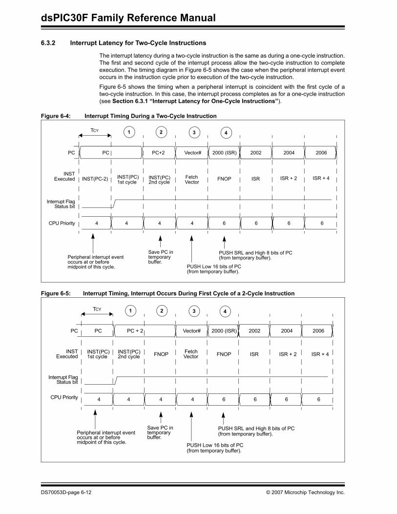
6.3.2 Interrupt Latency for Two-Cycle Instructions
The interrupt latency during a two-cycle instruction is the same as during a one-cycle instruction.The first and second cycle of the interrupt process allow the two-cycle instruction to completeexecution. The timing diagram in Figure 6-5 shows the case when the peripheral interrupt eventoccurs in the instruction cycle prior to execution of the two-cycle instruction.
Figure 6-5 shows the timing when a peripheral interrupt is coincident with the first cycle of atwo-cycle instruction. In this case, the interrupt process completes as for a one-cycle instruction(see Section 6.3.1 “Interrupt Latency for One-Cycle Instructions”).
Figure 6-4: Interrupt Timing During a Two-Cycle Instruction
Figure 6-5: Interrupt Timing, Interrupt Occurs During First Cycle of a 2-Cycle Instruction
4 6 6 64 4
INST(PC-2) INST(PC) INST(PC) FNOP ISRINST
Executed
Interrupt Flag
PUSH Low 16 bits of PC
PUSH SRL and High 8 bits of PC
64
ISR + 2 ISR + 4
CPU Priority
Fetch
2000 (ISR) 2002 2004 2006PC PC+2PC
Vector
Save PC in
Status bit
Vector#
Peripheral interrupt eventoccurs at or before
TCY 1 2 3 4
2nd cycle1st cycle
temporarybuffer.
midpoint of this cycle.
(from temporary buffer).
(from temporary buffer).
4 6 6 64 4
INST(PC) INST(PC) FNOP ISRINSTExecuted
Interrupt Flag
PUSH Low 16 bits of PC
PUSH SRL and High 8 bits of PC
64
ISR + 2 ISR + 4
CPU Priority
Fetch
2000 (ISR) 2002 2004 2006PC PC + 2PC
Vector
Save PC in
Status bit
Vector#
Peripheral interrupt eventoccurs at or before
TCY 1 2 3 4
2nd cycle1st cycle
temporarybuffer.
FNOP
midpoint of this cycle.(from temporary buffer).
(from temporary buffer).
DS70053D-page 6-12 © 2007 Microchip Technology Inc.
Section 6. InterruptsInterrupts
6
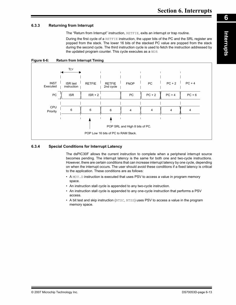
6.3.3 Returning from InterruptThe “Return from Interrupt” instruction, RETFIE, exits an interrupt or trap routine.
During the first cycle of a RETFIE instruction, the upper bits of the PC and the SRL register arepopped from the stack. The lower 16 bits of the stacked PC value are popped from the stackduring the second cycle. The third instruction cycle is used to fetch the instruction addressed bythe updated program counter. This cycle executes as a NOP.
Figure 6-6: Return from Interrupt Timing
6.3.4 Special Conditions for Interrupt Latency
The dsPIC30F allows the current instruction to complete when a peripheral interrupt sourcebecomes pending. The interrupt latency is the same for both one and two-cycle instructions.However, there are certain conditions that can increase interrupt latency by one cycle, dependingon when the interrupt occurs. The user should avoid these conditions if a fixed latency is criticalto the application. These conditions are as follows:
• A MOV.D instruction is executed that uses PSV to access a value in program memory space.
• An instruction stall cycle is appended to any two-cycle instruction.• An instruction stall cycle is appended to any one-cycle instruction that performs a PSV
access.• A bit test and skip instruction (BTSC, BTSS) uses PSV to access a value in the program
memory space.
4 4 4 46 6CPU
Priority
RETFIE RETFIE PCINSTExecuted
FNOPISR last
6
PC + 2 PC + 4
POP Low 16 bits of PC to RAM Stack.
POP SRL and High 8 bits of PC.
PC PC + 2 PC + 4 PC + 6ISR ISR + 2PC
2nd cycle
TCY
instruction
© 2007 Microchip Technology Inc. DS70053D-page 6-13

dsPIC30F Family Reference Manual
6.4 Interrupt Control and Status RegistersThe following registers are associated with the interrupt controller:
• INTCON1, INTCON2 RegistersGlobal interrupt control functions are derived from these two registers. INTCON1 contains the Interrupt Nesting Disable (NSTDIS) bit, as well as the control and status flags for the processor trap sources. The INTCON2 register controls the external interrupt request signal behavior and the use of the alternate vector table.
• IFSx: Interrupt Flag Status RegistersAll interrupt request flags are maintained in the IFSx registers, where ‘x’ denotes the register number. Each source of interrupt has a Status bit, which is set by the respective peripherals or external signal and is cleared via software.
• IECx: Interrupt Enable Control RegistersAll Interrupt Enable Control bits are maintained in the IECx registers, where ‘x’ denotes the register number. These control bits are used to individually enable interrupts from the peripherals or external signals.
• IPCx: Interrupt Priority Control RegistersEach user interrupt source can be assigned to one of eight priority levels. The IPC registers are used to set the interrupt priority level for each source of interrupt.
• SR: CPU Status Register The SR is not specifically part of the interrupt controller hardware, but it contains the IPL<2:0> Status bits (SR<7:5>) that indicate the current CPU priority level. The user may change the current CPU priority level by writing to the IPL bits.
• CORCON: Core Control Register The CORCON is not specifically part of the interrupt controller hardware, but it contains the IPL3 Status bit which indicates the current CPU priority level. IPL3 is a Read Only bit so that trap events cannot be masked by the user software.
Each register is described in detail on the following pages.
6.4.1 Assignment of Interrupts to Control Registers
The interrupt sources are assigned to the IFSx, IECx and IPCx registers in the same sequencethat they are listed in Table 6-2. For example, the INT0 (External Interrupt 0) is shown as hav-ing vector number and a natural order priority of ‘0’. Thus, the INT0IF Status bit is found inIFS0<0>. The INT0 interrupt uses bit 0 of the IEC0 register as its Enable bit and the IPC0<2:0>bits assign the interrupt priority level for the INT0 interrupt.
Note: The total number and type of interrupt sources will depend on the device variant.Refer to the specific device data sheet for further details.
DS70053D-page 6-14 © 2007 Microchip Technology Inc.

Section 6. InterruptsInterrupts
6
Register 6-1: SR: Status Register (In CPU)Register 6-2: CORCON: Core Control Register
Upper Byte:R-0 R-0 R/C-0 R/C-0 R-0 R/C-0 R-0 R-0OA OB SA SB OAB SAB DA DC
bit 15 bit 8
Lower Byte:R/W-0 R/W-0 R/W-0 R-0 R/W-0 R/W-0 R/W-0 R/W-0
IPL<2:0> RA N OV Z Cbit 7 bit 0
bit 7-5 IPL<2:0>: CPU Interrupt Priority Level Status bits111 = CPU interrupt priority level is 7 (15). User interrupts disabled.110 = CPU interrupt priority level is 6 (14)101 = CPU interrupt priority level is 5 (13)100 = CPU interrupt priority level is 4 (12)011 = CPU interrupt priority level is 3 (11)010 = CPU interrupt priority level is 2 (10)001 = CPU interrupt priority level is 1 (9)000 = CPU interrupt priority level is 0 (8)
Note 1: The IPL<2:0> bits are concatenated with the IPL<3> bit (CORCON<3>) to form the CPUinterrupt priority level. The value in parentheses indicates the IPL if IPL<3> = 1.
2: The IPL<2:0> status bits are read only when NSTDIS = 1 (INTCON1<15>).
Legend:R = Readable bit W = Writable bit U = Unimplemented bit, read as ‘0’ C = Bit can be cleared-n = Value at POR ‘1’ = Bit is set ‘0’ = Bit is cleared x = Bit is unknown
Upper Byte:U-0 U-0 U-0 R/W-0 R/W-0 R-0 R-0 R-0— — — US EDT DL<1:0>
bit 15 bit 8
Lower Byte:R/W-0 R/W-0 R/W-1 R/W-0 R/C-0 R/W-0 R/W-0 R/W-0SATA SATB SATDW ACCSAT IPL3 PSV RND IF
bit 7 bit 0
bit 3 IPL3: CPU Interrupt Priority Level Status bit 31 = CPU interrupt priority level is greater than 70 = CPU interrupt priority level is 7 or less
Note 1: The IPL3 bit is concatenated with the IPL<2:0> bits (SR<7:5>) to form the CPU interrupt prioritylevel.
Legend:R = Readable bit W = Writable bit U = Unimplemented bit, read as ‘0’ C = Bit can be cleared-n = Value at POR ‘1’ = Bit is set ‘0’ = Bit is cleared x = Bit is unknown
© 2007 Microchip Technology Inc. DS70053D-page 6-15

dsPIC30F Family Reference Manual
Register 6-3: INTCON1: Interrupt Control Register 1 Upper Byte:
R/W-0 U-0 U-0 U-0 U-0 R/W-0 R/W-0 R/W-0NSTDIS — — — — OVATE OVBTE COVTE
bit 15 bit 8
Lower Byte:U-0 U-0 U-0 R/W-0 R/W-0 R/W-0 R/W-0 U-0— — — MATHERR ADDRERR STKERR OSCFAIL —
bit 7 bit 0
bit 15 NSTDIS: Interrupt Nesting Disable bit1 = Interrupt nesting is disabled0 = Interrupt nesting is enabled
bit 14-11 Unimplemented: Read as ‘0’ bit 10 OVATE: Accumulator A Overflow Trap Enable bit
1 = Trap overflow of Accumulator A0 = Trap disabled
bit 9 OVBTE: Accumulator B Overflow Trap Enable bit1 = Trap overflow of Accumulator B0 = Trap disabled
bit 8 COVTE: Catastrophic Overflow Trap Enable bit1 = Trap on catastrophic overflow of Accumulator A or B enabled0 = Trap disabled
bit 7-5 Unimplemented: Read as ‘0’ bit 4 MATHERR: Arithmetic Error Status bit
1 = Overflow trap has occurred0 = Overflow trap has not occurred
bit 3 ADDRERR: Address Error Trap Status bit1 = Address error trap has occurred0 = Address error trap has not occurred
bit 2 STKERR: Stack Error Trap Status bit1 = Stack error trap has occurred0 = Stack error trap has not occurred
bit 1 OSCFAIL: Oscillator Failure Trap Status bit1 = Oscillator failure trap has occurred0 = Oscillator failure trap has not occurred
bit 0 Unimplemented: Read as ‘0’
Legend:R = Readable bit W = Writable bit U = Unimplemented bit, read as ‘0’-n = Value at POR ‘1’ = Bit is set ‘0’ = Bit is cleared x = Bit is unknown
DS70053D-page 6-16 © 2007 Microchip Technology Inc.

Section 6. InterruptsInterrupts
6
Register 6-4: INTCON2: Interrupt Control Register 2 Upper Byte:R/W-0 R-0 U-0 U-0 U-0 U-0 U-0 U-0ALTIVT DISI — — — — — —
bit 15 bit 8
Lower Byte:U-0 U-0 U-0 R/W-0 R/W-0 R/W-0 R/W-0 R/W-0— — — INT4EP INT3EP INT2EP INT1EP INT0EP
bit 7 bit 0
bit 15 ALTIVT: Enable Alternate Interrupt Vector Table bit1 = Use alternate vector table0 = Use standard (default) vector table
bit 14 DISI: DISI Instruction Status bit1 = DISI instruction is active0 = DISI is not active
bit 13-5 Unimplemented: Read as ‘0’ bit 4 INT4EP: External Interrupt 4 Edge Detect Polarity Select bit
1 = Interrupt on negative edge 0 = Interrupt on positive edge
bit 3 INT3EP: External Interrupt 3 Edge Detect Polarity Select bit1 = Interrupt on negative edge 0 = Interrupt on positive edge
bit 2 INT2EP: External Interrupt 2 Edge Detect Polarity Select bit1 = Interrupt on negative edge 0 = Interrupt on positive edge
bit 1 INT1EP: External Interrupt 1 Edge Detect Polarity Select bit1 = Interrupt on negative edge 0 = Interrupt on positive edge
bit 0 INT0EP: External Interrupt 0 Edge Detect Polarity Select bit1 = Interrupt on negative edge 0 = Interrupt on positive edge
Legend:R = Readable bit W = Writable bit U = Unimplemented bit, read as ‘0’-n = Value at POR ‘1’ = Bit is set ‘0’ = Bit is cleared x = Bit is unknown
© 2007 Microchip Technology Inc. DS70053D-page 6-17

dsPIC30F Family Reference Manual
Register 6-5: IFS0: Interrupt Flag Status Register 0 Upper Byte:
R/W-0 R/W-0 R/W-0 R/W-0 R/W-0 R/W-0 R/W-0 R/W-0CNIF MI2CIF SI2CIF NVMIF ADIF U1TXIF U1RXIF SPI1IF
bit 15 bit 8
Lower Byte:R/W-0 R/W-0 R/W-0 R/W-0 R/W-0 R/W-0 R/W-0 R/W-0T3IF T2IF OC2IF IC2IF T1IF OC1IF IC1IF INT0IF
bit 7 bit 0
bit 15 CNIF: Input Change Notification Flag Status bit1 = Interrupt request has occurred0 = Interrupt request has not occurred
bit 14 MI2CIF: I2C Bus Collision Flag Status bit1 = Interrupt request has occurred0 = Interrupt request has not occurred
bit 13 SI2CIF: I2C Transfer Complete Interrupt Flag Status bit1 = Interrupt request has occurred0 = Interrupt request has not occurred
bit 12 NVMIF: Non-Volatile Memory Write Complete Interrupt Flag Status bit1 = Interrupt request has occurred0 = Interrupt request has not occurred
bit 11 ADIF: A/D Conversion Complete Interrupt Flag Status bit1 = Interrupt request has occurred0 = Interrupt request has not occurred
bit 10 U1TXIF: UART1 Transmitter Interrupt Flag Status bit1 = Interrupt request has occurred0 = Interrupt request has not occurred
bit 9 U1RXIF: UART1 Receiver Interrupt Flag Status bit1 = Interrupt request has occurred0 = Interrupt request has not occurred
bit 8 SPI1IF: SPI1 Interrupt Flag Status bit1 = Interrupt request has occurred0 = Interrupt request has not occurred
bit 7 T3IF: Timer3 Interrupt Flag Status bit1 = Interrupt request has occurred0 = Interrupt request has not occurred
bit 6 T2IF: Timer2 Interrupt Flag Status bit1 = Interrupt request has occurred0 = Interrupt request has not occurred
bit 5 OC2IF: Output Compare Channel 2 Interrupt Flag Status bit1 = Interrupt request has occurred0 = Interrupt request has not occurred
bit 4 IC2IF: Input Capture Channel 2 Interrupt Flag Status bit1 = Interrupt request has occurred0 = Interrupt request has not occurred
bit 3 T1IF: Timer1 Interrupt Flag Status bit1 = Interrupt request has occurred0 = Interrupt request has not occurred
bit 2 OC1IF: Output Compare Channel 1 Interrupt Flag Status bit1 = Interrupt request has occurred0 = Interrupt request has not occurred
DS70053D-page 6-18 © 2007 Microchip Technology Inc.

Section 6. InterruptsInterrupts
6
Register 6-5: IFS0: Interrupt Flag Status Register 0 (Continued)bit 1 IC1IF: Input Capture Channel 1 Interrupt Flag Status bit1 = Interrupt request has occurred0 = Interrupt request has not occurred
bit 0 INT0IF: External Interrupt 0 Flag Status bit1 = Interrupt request has occurred0 = Interrupt request has not occurred
Legend:R = Readable bit W = Writable bit U = Unimplemented bit, read as ‘0’-n = Value at POR ‘1’ = Bit is set ‘0’ = Bit is cleared x = Bit is unknown
© 2007 Microchip Technology Inc. DS70053D-page 6-19
dsPIC30F Family Reference Manual
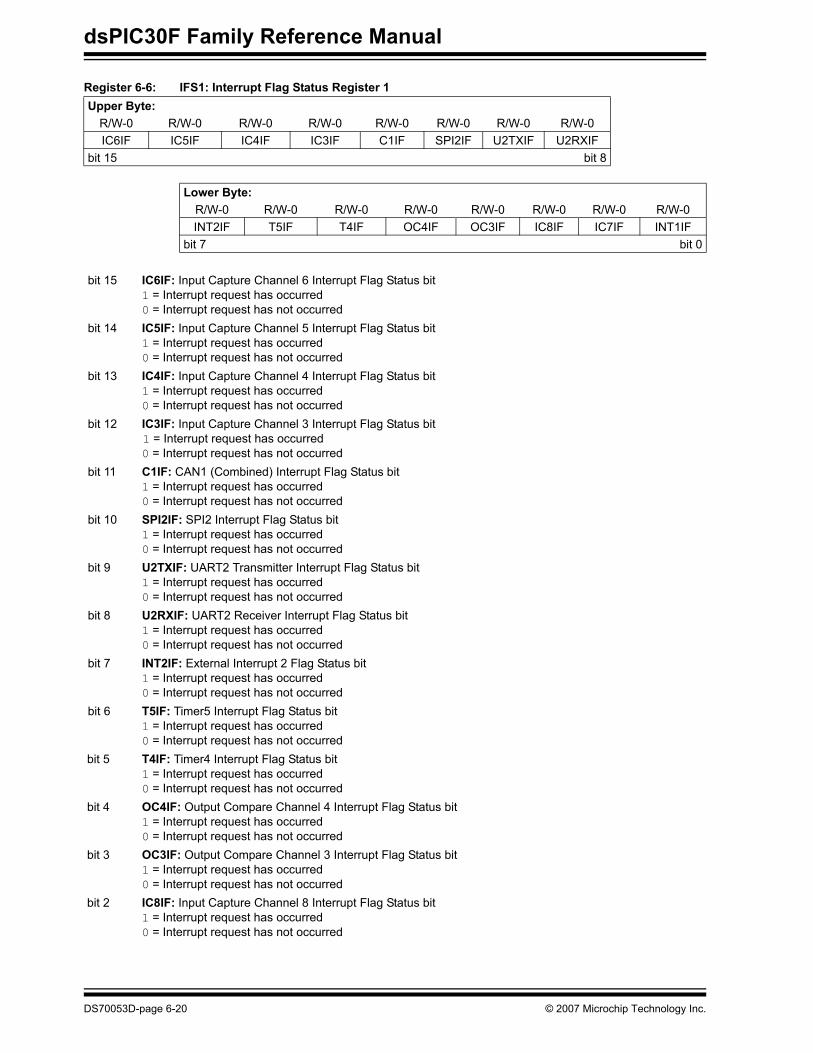
Register 6-6: IFS1: Interrupt Flag Status Register 1 Upper Byte:
R/W-0 R/W-0 R/W-0 R/W-0 R/W-0 R/W-0 R/W-0 R/W-0IC6IF IC5IF IC4IF IC3IF C1IF SPI2IF U2TXIF U2RXIF
bit 15 bit 8
Lower Byte:R/W-0 R/W-0 R/W-0 R/W-0 R/W-0 R/W-0 R/W-0 R/W-0INT2IF T5IF T4IF OC4IF OC3IF IC8IF IC7IF INT1IF
bit 7 bit 0
bit 15 IC6IF: Input Capture Channel 6 Interrupt Flag Status bit1 = Interrupt request has occurred0 = Interrupt request has not occurred
bit 14 IC5IF: Input Capture Channel 5 Interrupt Flag Status bit1 = Interrupt request has occurred0 = Interrupt request has not occurred
bit 13 IC4IF: Input Capture Channel 4 Interrupt Flag Status bit1 = Interrupt request has occurred0 = Interrupt request has not occurred
bit 12 IC3IF: Input Capture Channel 3 Interrupt Flag Status bit1 = Interrupt request has occurred0 = Interrupt request has not occurred
bit 11 C1IF: CAN1 (Combined) Interrupt Flag Status bit1 = Interrupt request has occurred0 = Interrupt request has not occurred
bit 10 SPI2IF: SPI2 Interrupt Flag Status bit1 = Interrupt request has occurred0 = Interrupt request has not occurred
bit 9 U2TXIF: UART2 Transmitter Interrupt Flag Status bit1 = Interrupt request has occurred0 = Interrupt request has not occurred
bit 8 U2RXIF: UART2 Receiver Interrupt Flag Status bit1 = Interrupt request has occurred0 = Interrupt request has not occurred
bit 7 INT2IF: External Interrupt 2 Flag Status bit1 = Interrupt request has occurred0 = Interrupt request has not occurred
bit 6 T5IF: Timer5 Interrupt Flag Status bit1 = Interrupt request has occurred0 = Interrupt request has not occurred
bit 5 T4IF: Timer4 Interrupt Flag Status bit1 = Interrupt request has occurred0 = Interrupt request has not occurred
bit 4 OC4IF: Output Compare Channel 4 Interrupt Flag Status bit1 = Interrupt request has occurred0 = Interrupt request has not occurred
bit 3 OC3IF: Output Compare Channel 3 Interrupt Flag Status bit1 = Interrupt request has occurred0 = Interrupt request has not occurred
bit 2 IC8IF: Input Capture Channel 8 Interrupt Flag Status bit1 = Interrupt request has occurred0 = Interrupt request has not occurred
DS70053D-page 6-20 © 2007 Microchip Technology Inc.

Section 6. InterruptsInterrupts
6
Register 6-6: IFS1: Interrupt Flag Status Register 1 (Continued)bit 1 IC7IF: Input Capture Channel 7 Interrupt Flag Status bit1 = Interrupt request has occurred0 = Interrupt request has not occurred
bit 0 INT1IF: External Interrupt 1 Flag Status bit1 = Interrupt request has occurred0 = Interrupt request has not occurred
Legend:R = Readable bit W = Writable bit U = Unimplemented bit, read as ‘0’-n = Value at POR ‘1’ = Bit is set ‘0’ = Bit is cleared x = Bit is unknown
© 2007 Microchip Technology Inc. DS70053D-page 6-21

dsPIC30F Family Reference Manual
Register 6-7: IFS2: Interrupt Flag Status Register 2 Upper Byte:
U-0 U-0 U-0 R/W-0 R/W-0 R/W-0 R/W-0 R/W-0— — — FLTBIF FLTAIF LVDIF DCIIF QEIIF
bit 15 bit 8
Lower Byte:R/W-0 R/W-0 R/W-0 R/W-0 R/W-0 R/W-0 R/W-0 R/W-0PWMIF C2IF INT4IF INT3IF OC8IF OC7IF OC6IF OC5IF
bit 7 bit 0
bit 15-13 Unimplemented: Read as ‘0’ bit 12 FLTBIF: Fault B Input Interrupt Flag Status bit
1 = Interrupt request has occurred0 = Interrupt request has not occurred
bit 11 FLTAIF: Fault A Input Interrupt Flag Status bit1 = Interrupt request has occurred0 = Interrupt request has not occurred
bit 10 LVDIF: Programmable Low Voltage Detect Interrupt Flag Status bit1 = Interrupt request has occurred0 = Interrupt request has not occurred
bit 9 DCIIF: Data Converter Interface Interrupt Flag Status bit1 = Interrupt request has occurred0 = Interrupt request has not occurred
bit 8 QEIIF: Quadrature Encoder Interface Interrupt Flag Status bit1 = Interrupt request has occurred0 = Interrupt request has not occurred
bit 7 PWMIF: Motor Control Pulse Width Modulation Interrupt Flag Status bit1 = Interrupt request has occurred0 = Interrupt request has not occurred
bit 6 C2IF: CAN2 (Combined) Interrupt Flag Status bit1 = Interrupt request has occurred0 = Interrupt request has not occurred
bit 5 INT4IF: External Interrupt 4 Flag Status bit1 = Interrupt request has occurred0 = Interrupt request has not occurred
bit 4 INT3IF: External Interrupt 3 Flag Status bit1 = Interrupt request has occurred0 = Interrupt request has not occurred
bit 3 OC8IF: Output Compare Channel 8 Interrupt Flag Status bit1 = Interrupt request has occurred0 = Interrupt request has not occurred
bit 2 OC7IF: Output Compare Channel 7 Interrupt Flag Status bit1 = Interrupt request has occurred0 = Interrupt request has not occurred
DS70053D-page 6-22 © 2007 Microchip Technology Inc.

Section 6. InterruptsInterrupts
6
Register 6-7: IFS2: Interrupt Flag Status Register 2 (Continued)bit 1 OC6IF: Output Compare Channel 6 Interrupt Flag Status bit1 = Interrupt request has occurred0 = Interrupt request has not occurred
bit 0 OC5IF: Output Compare Channel 5 Interrupt Flag Status bit1 = Interrupt request has occurred0 = Interrupt request has not occurred
Legend:R = Readable bit W = Writable bit U = Unimplemented bit, read as ‘0’-n = Value at POR ‘1’ = Bit is set ‘0’ = Bit is cleared x = Bit is unknown
© 2007 Microchip Technology Inc. DS70053D-page 6-23
dsPIC30F Family Reference Manual
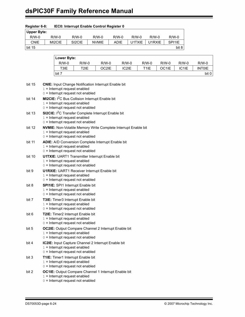
Register 6-8: IEC0: Interrupt Enable Control Register 0 Upper Byte:
R/W-0 R/W-0 R/W-0 R/W-0 R/W-0 R/W-0 R/W-0 R/W-0CNIE MI2CIE SI2CIE NVMIE ADIE U1TXIE U1RXIE SPI1IE
bit 15 bit 8
Lower Byte:R/W-0 R/W-0 R/W-0 R/W-0 R/W-0 R/W-0 R/W-0 R/W-0T3IE T2IE OC2IE IC2IE T1IE OC1IE IC1IE INT0IE
bit 7 bit 0
bit 15 CNIE: Input Change Notification Interrupt Enable bit1 = Interrupt request enabled0 = Interrupt request not enabled
bit 14 MI2CIE: I2C Bus Collision Interrupt Enable bit1 = Interrupt request enabled0 = Interrupt request not enabled
bit 13 SI2CIE: I2C Transfer Complete Interrupt Enable bit1 = Interrupt request enabled0 = Interrupt request not enabled
bit 12 NVMIE: Non-Volatile Memory Write Complete Interrupt Enable bit1 = Interrupt request enabled0 = Interrupt request not enabled
bit 11 ADIE: A/D Conversion Complete Interrupt Enable bit1 = Interrupt request enabled0 = Interrupt request not enabled
bit 10 U1TXIE: UART1 Transmitter Interrupt Enable bit1 = Interrupt request enabled0 = Interrupt request not enabled
bit 9 U1RXIE: UART1 Receiver Interrupt Enable bit1 = Interrupt request enabled0 = Interrupt request not enabled
bit 8 SPI1IE: SPI1 Interrupt Enable bit1 = Interrupt request enabled0 = Interrupt request not enabled
bit 7 T3IE: Timer3 Interrupt Enable bit1 = Interrupt request enabled0 = Interrupt request not enabled
bit 6 T2IE: Timer2 Interrupt Enable bit1 = Interrupt request enabled0 = Interrupt request not enabled
bit 5 OC2IE: Output Compare Channel 2 Interrupt Enable bit1 = Interrupt request enabled0 = Interrupt request not enabled
bit 4 IC2IE: Input Capture Channel 2 Interrupt Enable bit1 = Interrupt request enabled0 = Interrupt request not enabled
bit 3 T1IE: Timer1 Interrupt Enable bit1 = Interrupt request enabled0 = Interrupt request not enabled
bit 2 OC1IE: Output Compare Channel 1 Interrupt Enable bit1 = Interrupt request enabled0 = Interrupt request not enabled
DS70053D-page 6-24 © 2007 Microchip Technology Inc.
Section 6. InterruptsInterrupts
6
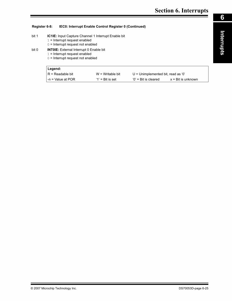
Register 6-8: IEC0: Interrupt Enable Control Register 0 (Continued)bit 1 IC1IE: Input Capture Channel 1 Interrupt Enable bit1 = Interrupt request enabled0 = Interrupt request not enabled
bit 0 INT0IE: External Interrupt 0 Enable bit1 = Interrupt request enabled0 = Interrupt request not enabled
Legend:R = Readable bit W = Writable bit U = Unimplemented bit, read as ‘0’-n = Value at POR ‘1’ = Bit is set ‘0’ = Bit is cleared x = Bit is unknown
© 2007 Microchip Technology Inc. DS70053D-page 6-25

dsPIC30F Family Reference Manual
Register 6-9: IEC1: Interrupt Enable Control Register 1 Upper Byte:
R/W-0 R/W-0 R/W-0 R/W-0 R/W-0 R/W-0 R/W-0 R/W-0IC6IE IC5IE IC4IE IC3IE C1IE SPI2IE U2TXIE U2RXIE
bit 15 bit 8
Lower Byte:R/W-0 R/W-0 R/W-0 R/W-0 R/W-0 R/W-0 R/W-0 R/W-0INT2IE T5IE T4IE OC4IE OC3IE IC8IE IC7IE INT1IE
bit 7 bit 0
bit 15 IC6IE: Input Capture Channel 6 Interrupt Enable bit1 = Interrupt request enabled0 = Interrupt request not enabled
bit 14 IC5IE: Input Capture Channel 5 Interrupt Enable bit1 = Interrupt request enabled0 = Interrupt request not enabled
bit 13 IC4IE: Input Capture Channel 4 Interrupt Enable bit1 = Interrupt request enabled0 = Interrupt request not enabled
bit 12 IC3IE: Input Capture Channel 3 Interrupt Enable bit1 = Interrupt request enabled0 = Interrupt request not enabled
bit 11 C1IE: CAN1 (Combined) Interrupt Enable bit1 = Interrupt request enabled0 = Interrupt request not enabled
bit 10 SPI2IE: SPI2 Interrupt Enable bit1 = Interrupt request enabled0 = Interrupt request not enabled
bit 9 U2TXIE: UART2 Transmitter Interrupt Enable bit1 = Interrupt request enabled0 = Interrupt request not enabled
bit 8 U2RXIE: UART2 Receiver Interrupt Enable bit1 = Interrupt request enabled0 = Interrupt request not enabled
bit 7 INT2IE: External Interrupt 2 Enable bit1 = Interrupt request enabled0 = Interrupt request not enabled
bit 6 T5IE: Timer5 Interrupt Enable bit1 = Interrupt request enabled0 = Interrupt request not enabled
bit 5 T4IE: Timer4 Interrupt Enable bit1 = Interrupt request enabled0 = Interrupt request not enabled
bit 4 OC4IE: Output Compare Channel 4 Interrupt Enable bit1 = Interrupt request enabled0 = Interrupt request not enabled
bit 3 OC3IE: Output Compare Channel 3 Interrupt Enable bit1 = Interrupt request enabled0 = Interrupt request not enabled
bit 2 IC8IE: Input Capture Channel 8 Interrupt Enable bit1 = Interrupt request enabled0 = Interrupt request not enabled
DS70053D-page 6-26 © 2007 Microchip Technology Inc.

Section 6. InterruptsInterrupts
6
Register 6-9: IEC1: Interrupt Enable Control Register 1 (Continued)bit 1 IC7IE: Input Capture Channel 7 Interrupt Enable bit1 = Interrupt request enabled0 = Interrupt request not enabled
bit 0 INT1IE: External Interrupt 1 Enable bit1 = Interrupt request enabled0 = Interrupt request not enabled
Legend:R = Readable bit W = Writable bit U = Unimplemented bit, read as ‘0’-n = Value at POR ‘1’ = Bit is set ‘0’ = Bit is cleared x = Bit is unknown
© 2007 Microchip Technology Inc. DS70053D-page 6-27

dsPIC30F Family Reference Manual
Register 6-10: IEC2: Interrupt Enable Control Register 2 Upper Byte:
U-0 U-0 U-0 R/W-0 R/W-0 R/W-0 R/W-0 R/W-0— — — FLTBIE FLTAIE LVDIE DCIIE QEIIE
bit 15 bit 8
Lower Byte:R/W-0 R/W-0 R/W-0 R/W-0 R/W-0 R/W-0 R/W-0 R/W-0
PWMIE C2IE INT4IE INT3IE OC8IE OC7IE OC6IE OC5IEbit 7 bit 0
bit 15-13 Unimplemented: Read as ‘0’ bit 12 FLTBIE: Fault B Input Interrupt Enable bit
1 = Interrupt request enabled0 = Interrupt request not enabled
bit 11 FLTAIE: Fault A Interrupt Enable bit1 = Interrupt request enabled0 = Interrupt request not enabled
bit 10 LVDIE: Programmable Low Voltage Detect Interrupt Enable bit1 = Interrupt request enabled0 = Interrupt request not enabled
bit 9 DCIIE: Data Converter Interface Interrupt Enable bit1 = Interrupt request enabled0 = Interrupt request not enabled
bit 8 QEIIE: Quadrature Encoder Interface Interrupt Enable bit1 = Interrupt request enabled0 = Interrupt request not enabled
bit 7 PWMIE: Motor Control Pulse Width Modulation Interrupt Enable bit1 = Interrupt request enabled0 = Interrupt request not enabled
bit 6 C2IE: CAN2 (Combined) Interrupt Enable bit1 = Interrupt request enabled0 = Interrupt request not enabled
bit 5 INT4IE: External Interrupt 4 Enable bit1 = Interrupt request enabled0 = Interrupt request not enabled
bit 4 INT3IE: External Interrupt 3 Enable bit1 = Interrupt request enabled0 = Interrupt request not enabled
bit 3 OC8IE: Output Compare Channel 8 Interrupt Enable bit1 = Interrupt request enabled0 = Interrupt request not enabled
bit 2 OC7IE: Output Compare Channel 7 Interrupt Enable bit1 = Interrupt request enabled0 = Interrupt request not enabled
DS70053D-page 6-28 © 2007 Microchip Technology Inc.

Section 6. InterruptsInterrupts
6
Register 6-10: IEC2: Interrupt Enable Control Register 2 (Continued)bit 1 OC6IE: Output Compare Channel 6 Interrupt Enable bit1 = Interrupt request enabled0 = Interrupt request not enabled
bit 0 OC5IE: Output Compare Channel 5 Interrupt Enable bit1 = Interrupt request enabled0 = Interrupt request not enabled
Legend:R = Readable bit W = Writable bit U = Unimplemented bit, read as ‘0’-n = Value at POR ‘1’ = Bit is set ‘0’ = Bit is cleared x = Bit is unknown
© 2007 Microchip Technology Inc. DS70053D-page 6-29

dsPIC30F Family Reference Manual
Register 6-11: IPC0: Interrupt Priority Control Register 0 Upper Byte:
U-0 R/W-1 R/W-0 R/W-0 U-0 R/W-1 R/W-0 R/W-0— T1IP<2:0> — OC1IP<2:0>
bit 15 bit 8
Lower Byte:U-0 R/W-1 R/W-0 R/W-0 U-0 R/W-1 R/W-0 R/W-0— IC1IP<2:0> — INT0IP<2:0>
bit 7 bit 0
bit 15 Unimplemented: Read as ‘0’ bit 14-12 T1IP<2:0>: Timer1 Interrupt Priority bits
111 = Interrupt is priority 7 (highest priority interrupt)•••001 = Interrupt is priority 1000 = Interrupt source is disabled
bit 11 Unimplemented: Read as ‘0’ bit 10-8 OC1IP<2:0>: Output Compare Channel 1 Interrupt Priority bits
111 = Interrupt is priority 7 (highest priority interrupt)•••001 = Interrupt is priority 1000 = Interrupt source is disabled
bit 7 Unimplemented: Read as ‘0’ bit 6-4 IC1IP<2:0>: Input Capture Channel 1 Interrupt Priority bits
111 = Interrupt is priority 7 (highest priority interrupt)•••001 = Interrupt is priority 1000 = Interrupt source is disabled
bit 3 Unimplemented: Read as ‘0’ bit 2-0 INT0IP<2:0>: External Interrupt 0 Priority bits
111 = Interrupt is priority 7 (highest priority interrupt)•••001 = Interrupt is priority 1000 = Interrupt source is disabled
Legend:R = Readable bit W = Writable bit U = Unimplemented bit, read as ‘0’-n = Value at POR ‘1’ = Bit is set ‘0’ = Bit is cleared x = Bit is unknown
DS70053D-page 6-30 © 2007 Microchip Technology Inc.

Section 6. InterruptsInterrupts
6
Register 6-12: IPC1: Interrupt Priority Control Register 1 Upper Byte:U-0 R/W-1 R/W-0 R/W-0 U-0 R/W-1 R/W-0 R/W-0— T3IP<2:0> — T2IP<2:0>
bit 15 bit 8
Lower Byte:U-0 R/W-1 R/W-0 R/W-0 U-0 R/W-1 R/W-0 R/W-0— OC2IP<2:0> — IC2IP<2:0>
bit 7 bit 0
bit 15 Unimplemented: Read as ‘0’ bit 14-12 T3IP<2:0>: Timer3 Interrupt Priority bits
111 = Interrupt is priority 7 (highest priority interrupt)•••001 = Interrupt is priority 1000 = Interrupt source is disabled
bit 11 Unimplemented: Read as ‘0’ bit 10-8 T2IP<2:0>: Timer2 Interrupt Priority bits
111 = Interrupt is priority 7 (highest priority interrupt)•••001 = Interrupt is priority 1000 = Interrupt source is disabled
bit 7 Unimplemented: Read as ‘0’ bit 6-4 OC2IP<2:0>: Output Compare Channel 2 Interrupt Priority bits
111 = Interrupt is priority 7 (highest priority interrupt)•••001 = Interrupt is priority 1000 = Interrupt source is disabled
bit 3 Unimplemented: Read as ‘0’ bit 2-0 IC2IP<2:0>: Input Capture Channel 2 Interrupt Priority bits
111 = Interrupt is priority 7 (highest priority interrupt)•••001 = Interrupt is priority 1000 = Interrupt source is disabled
Legend:R = Readable bit W = Writable bit U = Unimplemented bit, read as ‘0’-n = Value at POR ‘1’ = Bit is set ‘0’ = Bit is cleared x = Bit is unknown
© 2007 Microchip Technology Inc. DS70053D-page 6-31
dsPIC30F Family Reference Manual
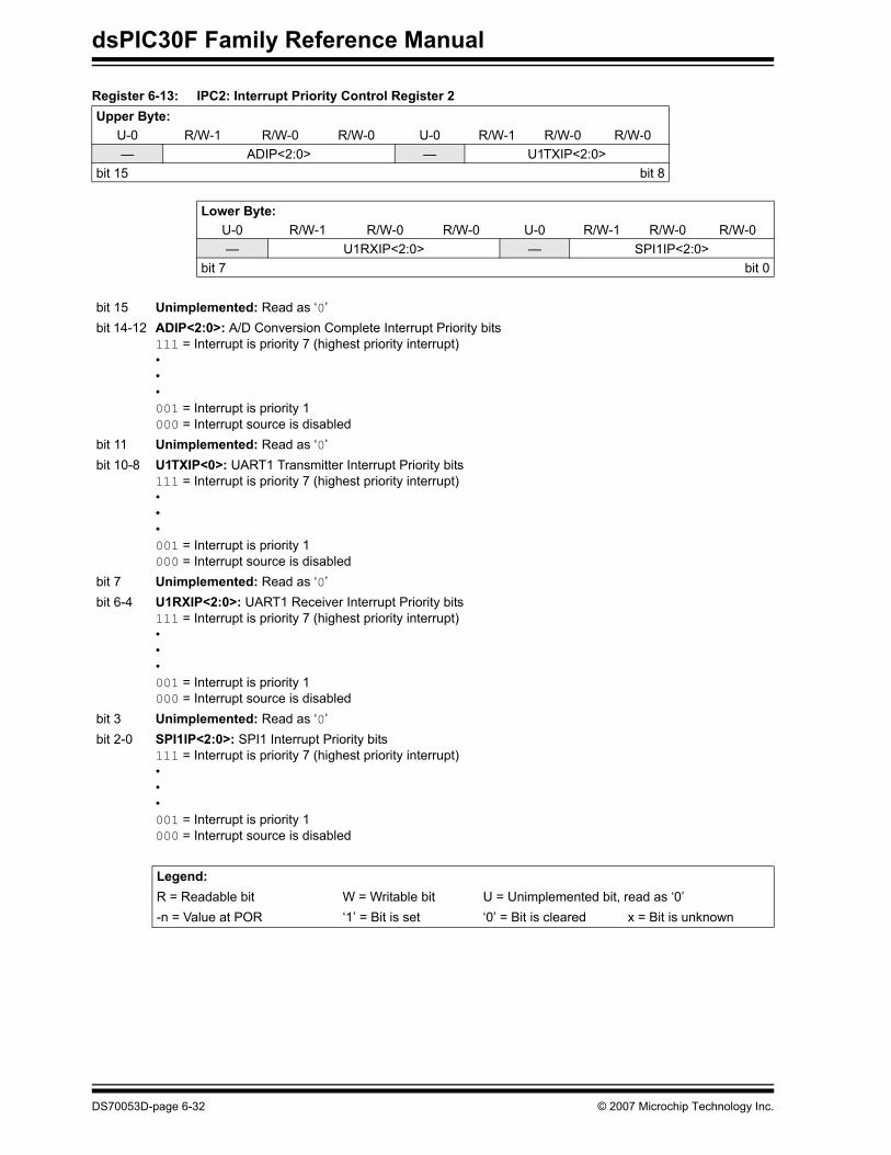
Register 6-13: IPC2: Interrupt Priority Control Register 2 Upper Byte:
U-0 R/W-1 R/W-0 R/W-0 U-0 R/W-1 R/W-0 R/W-0— ADIP<2:0> — U1TXIP<2:0>
bit 15 bit 8
Lower Byte:U-0 R/W-1 R/W-0 R/W-0 U-0 R/W-1 R/W-0 R/W-0— U1RXIP<2:0> — SPI1IP<2:0>
bit 7 bit 0
bit 15 Unimplemented: Read as ‘0’ bit 14-12 ADIP<2:0>: A/D Conversion Complete Interrupt Priority bits
111 = Interrupt is priority 7 (highest priority interrupt)•••001 = Interrupt is priority 1000 = Interrupt source is disabled
bit 11 Unimplemented: Read as ‘0’ bit 10-8 U1TXIP<0>: UART1 Transmitter Interrupt Priority bits
111 = Interrupt is priority 7 (highest priority interrupt)•••001 = Interrupt is priority 1000 = Interrupt source is disabled
bit 7 Unimplemented: Read as ‘0’ bit 6-4 U1RXIP<2:0>: UART1 Receiver Interrupt Priority bits
111 = Interrupt is priority 7 (highest priority interrupt)•••001 = Interrupt is priority 1000 = Interrupt source is disabled
bit 3 Unimplemented: Read as ‘0’ bit 2-0 SPI1IP<2:0>: SPI1 Interrupt Priority bits
111 = Interrupt is priority 7 (highest priority interrupt)•••001 = Interrupt is priority 1000 = Interrupt source is disabled
Legend:R = Readable bit W = Writable bit U = Unimplemented bit, read as ‘0’-n = Value at POR ‘1’ = Bit is set ‘0’ = Bit is cleared x = Bit is unknown
DS70053D-page 6-32 © 2007 Microchip Technology Inc.

Section 6. InterruptsInterrupts
6
Register 6-14: IPC3: Interrupt Priority Control Register 3 Upper Byte:U-0 R/W-1 R/W-0 R/W-0 U-0 R/W-1 R/W-0 R/W-0— CNIP<2:0> — MI2CIP<2:0>
bit 15 bit 8
Lower Byte:U-0 R/W-1 R/W-0 R/W-0 U-0 R/W-1 R/W-0 R/W-0— SI2CIP<2:0> — NVMIP<2:0>
bit 7 bit 0
bit 15 Unimplemented: Read as ‘0’ bit 14-12 CNIP<2:0>: Input Change Notification Interrupt Priority bits
111 = Interrupt is priority 7 (highest priority interrupt)•••001 = Interrupt is priority 1000 = Interrupt source is disabled
bit 11 Unimplemented: Read as ‘0’ bit 10-8 MI2CIP<2:0>: I2C Bus Collision Interrupt Priority bits
111 = Interrupt is priority 7 (highest priority interrupt)•••001 = Interrupt is priority 1000 = Interrupt source is disabled
bit 7 Unimplemented: Read as ‘0’ bit 6-4 SI2CIP<2:0>: I2C Transfer Complete Interrupt Priority bits
111 = Interrupt is priority 7 (highest priority interrupt)•••001 = Interrupt is priority 1000 = Interrupt source is disabled
bit 3 Unimplemented: Read as ‘0’ bit 2-0 NVMIP<2:0>: Non-Volatile Memory Write Interrupt Priority bits
111 = Interrupt is priority 7 (highest priority interrupt)•••001 = Interrupt is priority 1000 = Interrupt source is disabled
Legend:R = Readable bit W = Writable bit U = Unimplemented bit, read as ‘0’-n = Value at POR ‘1’ = Bit is set ‘0’ = Bit is cleared x = Bit is unknown
© 2007 Microchip Technology Inc. DS70053D-page 6-33

dsPIC30F Family Reference Manual
Register 6-15: IPC4: Interrupt Priority Control Register 4 Upper Byte:
U-0 R/W-1 R/W-0 R/W-0 U-0 R/W-1 R/W-0 R/W-0— OC3IP<2:0> — IC8IP<2:0>
bit 15 bit 8
Lower Byte:U-0 R/W-1 R/W-0 R/W-0 U-0 R/W-1 R/W-0 R/W-0— IC7IP<2:0> — INT1IP<2:0>
bit 7 bit 0
bit 15 Unimplemented: Read as ‘0’ bit 14-12 OC3IP<2:0>: Output Compare Channel 3 Interrupt Priority bits
111 = Interrupt is priority 7 (highest priority interrupt)•••001 = Interrupt is priority 1000 = Interrupt source is disabled
bit 11 Unimplemented: Read as ‘0’ bit 10-8 IC8IP<2:0>: Input Capture Channel 8 Interrupt Priority bits
111 = Interrupt is priority 7 (highest priority interrupt)•••001 = Interrupt is priority 1000 = Interrupt source is disabled
bit 7 Unimplemented: Read as ‘0’ bit 6-4 IC7IP<2:0>: Input Capture Channel 7 Interrupt Priority bits
111 = Interrupt is priority 7 (highest priority interrupt)•••001 = Interrupt is priority 1000 = Interrupt source is disabled
bit 3 Unimplemented: Read as ‘0’ bit 2-0 INT1IP<2:0>: External Interrupt 1 Priority bits
111 = Interrupt is priority 7 (highest priority interrupt)•••001 = Interrupt is priority 1000 = Interrupt source is disabled
Legend:R = Readable bit W = Writable bit U = Unimplemented bit, read as ‘0’-n = Value at POR ‘1’ = Bit is set ‘0’ = Bit is cleared x = Bit is unknown
DS70053D-page 6-34 © 2007 Microchip Technology Inc.

Section 6. InterruptsInterrupts
6
Register 6-16: IPC5: Interrupt Priority Control Register 5 Upper Byte:U-0 R/W-1 R/W-0 R/W-0 U-0 R/W-1 R/W-0 R/W-0— INT2IP<2:0> — T5IP<2:0>
bit 15 bit 8
Lower Byte:U-0 R/W-1 R/W-0 R/W-0 U-0 R/W-1 R/W-0 R/W-0— T4IP<2:0> — OC4IP<2:0>
bit 7 bit 0
bit 15 Unimplemented: Read as ‘0’ bit 14-12 INT2IP<2:0>: External Interrupt 2 Priority bits
111 = Interrupt is priority 7 (highest priority interrupt)•••001 = Interrupt is priority 1000 = Interrupt source is disabled
bit 11 Unimplemented: Read as ‘0’ bit 10-8 T5IP<2:0>: Timer5 Interrupt Priority bits
111 = Interrupt is priority 7 (highest priority interrupt)•••001 = Interrupt is priority 1000 = Interrupt source is disabled
bit 7 Unimplemented: Read as ‘0’ bit 6-4 T4IP<2:0>: Timer4 Interrupt Priority bits
111 = Interrupt is priority 7 (highest priority interrupt)•••001 = Interrupt is priority 1000 = Interrupt source is disabled
bit 3 Unimplemented: Read as ‘0’ bit 2-0 OC4IP<2:0>: Output Compare Channel 4 Interrupt Priority bits
111 = Interrupt is priority 7 (highest priority interrupt)•••001 = Interrupt is priority 1000 = Interrupt source is disabled
Legend:R = Readable bit W = Writable bit U = Unimplemented bit, read as ‘0’-n = Value at POR ‘1’ = Bit is set ‘0’ = Bit is cleared x = Bit is unknown
© 2007 Microchip Technology Inc. DS70053D-page 6-35
dsPIC30F Family Reference Manual
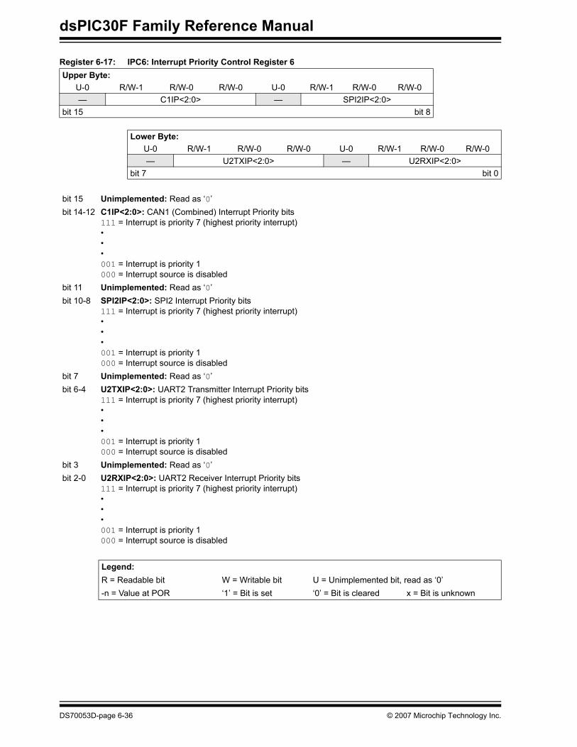
Register 6-17: IPC6: Interrupt Priority Control Register 6 Upper Byte:
U-0 R/W-1 R/W-0 R/W-0 U-0 R/W-1 R/W-0 R/W-0— C1IP<2:0> — SPI2IP<2:0>
bit 15 bit 8
Lower Byte:U-0 R/W-1 R/W-0 R/W-0 U-0 R/W-1 R/W-0 R/W-0— U2TXIP<2:0> — U2RXIP<2:0>
bit 7 bit 0
bit 15 Unimplemented: Read as ‘0’ bit 14-12 C1IP<2:0>: CAN1 (Combined) Interrupt Priority bits
111 = Interrupt is priority 7 (highest priority interrupt)•••001 = Interrupt is priority 1000 = Interrupt source is disabled
bit 11 Unimplemented: Read as ‘0’ bit 10-8 SPI2IP<2:0>: SPI2 Interrupt Priority bits
111 = Interrupt is priority 7 (highest priority interrupt)•••001 = Interrupt is priority 1000 = Interrupt source is disabled
bit 7 Unimplemented: Read as ‘0’ bit 6-4 U2TXIP<2:0>: UART2 Transmitter Interrupt Priority bits
111 = Interrupt is priority 7 (highest priority interrupt)•••001 = Interrupt is priority 1000 = Interrupt source is disabled
bit 3 Unimplemented: Read as ‘0’ bit 2-0 U2RXIP<2:0>: UART2 Receiver Interrupt Priority bits
111 = Interrupt is priority 7 (highest priority interrupt)•••001 = Interrupt is priority 1000 = Interrupt source is disabled
Legend:R = Readable bit W = Writable bit U = Unimplemented bit, read as ‘0’-n = Value at POR ‘1’ = Bit is set ‘0’ = Bit is cleared x = Bit is unknown
DS70053D-page 6-36 © 2007 Microchip Technology Inc.

Section 6. InterruptsInterrupts
6
Register 6-18: IPC7: Interrupt Priority Control Register 7 Upper Byte:U-0 R/W-1 R/W-0 R/W-0 U-0 R/W-1 R/W-0 R/W-0— IC6IP<2:0> — IC5IP<2:0>
bit 15 bit 8
Lower Byte:U-0 R/W-1 R/W-0 R/W-0 U-0 R/W-1 R/W-0 R/W-0— IC4IP<2:0> — IC3IP<2:0>
bit 7 bit 0
bit 15 Unimplemented: Read as ‘0’ bit 14-12 IC6IP<2:0>: Input Capture Channel 6 Interrupt Priority bits
111 = Interrupt is priority 7 (highest priority interrupt)•••001 = Interrupt is priority 1000 = Interrupt source is disabled
bit 11 Unimplemented: Read as ‘0’ bit 10-8 IC5IP<2:0>: Input Capture Channel 5 Interrupt Priority bits
111 = Interrupt is priority 7 (highest priority interrupt)•••001 = Interrupt is priority 1000 = Interrupt source is disabled
bit 7 Unimplemented: Read as ‘0’ bit 6-4 IC4IP<2:0>: Input Capture Channel 4 Interrupt Priority bits
111 = Interrupt is priority 7 (highest priority interrupt)•••001 = Interrupt is priority 1000 = Interrupt source is disabled
bit 3 Unimplemented: Read as ‘0’ bit 2-0 IC3IP<2:0>: Input Capture Channel 3 Interrupt Priority bits
111 = Interrupt is priority 7 (highest priority interrupt)•••001 = Interrupt is priority 1000 = Interrupt source is disabled
Legend:R = Readable bit W = Writable bit U = Unimplemented bit, read as ‘0’-n = Value at POR ‘1’ = Bit is set ‘0’ = Bit is cleared x = Bit is unknown
© 2007 Microchip Technology Inc. DS70053D-page 6-37

dsPIC30F Family Reference Manual
Register 6-19: IPC8: Interrupt Priority Control Register 8 Upper Byte:
U-0 R/W-1 R/W-0 R/W-0 U-0 R/W-1 R/W-0 R/W-0— OC8IP<2:0> — OC7IP<2:0>
bit 15 bit 8
Lower Byte:U-0 R/W-1 R/W-0 R/W-0 U-0 R/W-1 R/W-0 R/W-0— OC6IP<2:0> — OC5IP<2:0>
bit 7 bit 0
bit 15 Unimplemented: Read as ‘0’ bit 14-12 OC8IP<2:0>: Output Compare Channel 8 Interrupt Priority bits
111 = Interrupt is priority 7 (highest priority interrupt)•••001 = Interrupt is priority 1000 = Interrupt source is disabled
bit 11 Unimplemented: Read as ‘0’ bit 10-8 OC7IP<2:0>: Output Compare Channel 7 Interrupt Priority bits
111 = Interrupt is priority 7 (highest priority interrupt)•••001 = Interrupt is priority 1000 = Interrupt source is disabled
bit 7 Unimplemented: Read as ‘0’ bit 6-4 OC6IP<2:0>: Output Compare Channel 6 Interrupt Priority bits
111 = Interrupt is priority 7 (highest priority interrupt)•••001 = Interrupt is priority 1000 = Interrupt source is disabled
bit 3 Unimplemented: Read as ‘0’ bit 2-0 OC5IP<2:0>: Output Compare Channel 5 Interrupt Priority bits
111 = Interrupt is priority 7 (highest priority interrupt)•••001 = Interrupt is priority 1000 = Interrupt source is disabled
Legend:R = Readable bit W = Writable bit U = Unimplemented bit, read as ‘0’-n = Value at POR ‘1’ = Bit is set ‘0’ = Bit is cleared x = Bit is unknown
DS70053D-page 6-38 © 2007 Microchip Technology Inc.

Section 6. InterruptsInterrupts
6
Register 6-20: IPC9: Interrupt Priority Control Register 9 Upper Byte:U-0 R/W-1 R/W-0 R/W-0 U-0 R/W-1 R/W-0 R/W-0— PWMIP<2:0> — C2IP<2:0>
bit 15 bit 8
Lower Byte:U-0 R/W-1 R/W-0 R/W-0 U-0 R/W-1 R/W-0 R/W-0— INT4IP<2:0> — INT3IP<2:0>
bit 7 bit 0
bit 15 Unimplemented: Read as ‘0’ bit 14-12 PWMIP<2:0>: Motor Control Pulse Width Modulation Interrupt Priority bits
111 = Interrupt is priority 7 (highest priority interrupt)•••001 = Interrupt is priority 1000 = Interrupt source is disabled
bit 11 Unimplemented: Read as ‘0’ bit 10-8 C2IP<2:0>: CAN2 (Combined) Interrupt Priority bits
111 = Interrupt is priority 7 (highest priority interrupt)•••001 = Interrupt is priority 1000 = Interrupt source is disabled
bit 7 Unimplemented: Read as ‘0’ bit 6-4 INT4IP<2:0>: External Interrupt 4 Priority bits
111 = Interrupt is priority 7 (highest priority interrupt)•••001 = Interrupt is priority 1000 = Interrupt source is disabled
bit 3 Unimplemented: Read as ‘0’ bit 2-0 INT3IP<2:0>: External Interrupt 3 Priority bits
111 = Interrupt is priority 7 (highest priority interrupt)•••001 = Interrupt is priority 1000 = Interrupt source is disabled
Legend:R = Readable bit W = Writable bit U = Unimplemented bit, read as ‘0’-n = Value at POR ‘1’ = Bit is set ‘0’ = Bit is cleared x = Bit is unknown
© 2007 Microchip Technology Inc. DS70053D-page 6-39

dsPIC30F Family Reference Manual
Register 6-21: IPC10: Interrupt Priority Control Register 10 Upper Byte:
U-0 R/W-1 R/W-0 R/W-0 U-0 R/W-1 R/W-0 R/W-0— FLTAIP<2:0> — LVDIP<2:0>
bit 15 bit 8
Lower Byte:U-0 R/W-1 R/W-0 R/W-0 U-0 R/W-1 R/W-0 R/W-0— DCIIP<2:0> — QEIIP<2:0>
bit 7 bit 0
bit 15 Unimplemented: Read as ‘0’ bit 14-12 FLTAIP<2:0>: Fault A Input Interrupt Priority bits
111 = Interrupt is priority 7 (highest priority interrupt)•••001 = Interrupt is priority 1000 = Interrupt source is disabled
bit 11 Unimplemented: Read as ‘0’ bit 10-8 LVDIP<2:0>: Programmable Low Voltage Detect Interrupt Priority bits
111 = Interrupt is priority 7 (highest priority interrupt)•••001 = Interrupt is priority 1000 = Interrupt source is disabled
bit 7 Unimplemented: Read as ‘0’ bit 6-4 DCIIP<2:0>: Data Converter Interface Interrupt Priority bits
111 = Interrupt is priority 7 (highest priority interrupt)•••001 = Interrupt is priority 1000 = Interrupt source is disabled
bit 3 Unimplemented: Read as ‘0’ bit 2-0 QEIIP<2:0>: Quadrature Encoder Interface Interrupt Priority bits
111 = Interrupt is priority 7 (highest priority interrupt)•••001 = Interrupt is priority 1000 = Interrupt source is disabled
Legend:R = Readable bit W = Writable bit U = Unimplemented bit, read as ‘0’-n = Value at POR ‘1’ = Bit is set ‘0’ = Bit is cleared x = Bit is unknown
DS70053D-page 6-40 © 2007 Microchip Technology Inc.

Section 6. InterruptsInterrupts
6
Register 6-22: IPC11: Interrupt Priority Control Register 11 Upper Byte:U-0 U-0 U-0 U-0 U-0 U-0 U-0 U-0— — — — — — — —
bit 15 bit 8
Lower Byte:U-0 U-0 U-0 U-0 U-0 R/W-1 R/W-0 R/W-0— — — — — FLTBIP<2:0>
bit 7 bit 0
bit 15-3 Unimplemented: Read as ‘0’ bit 2-0 FLTBIP<2:0>: Fault B Input Interrupt Priority bits
111 = Interrupt is priority 7 (highest priority interrupt)•••001 = Interrupt is priority 1000 = Interrupt source is disabled
Legend:R = Readable bit W = Writable bit U = Unimplemented bit, read as ‘0’-n = Value at POR ‘1’ = Bit is set ‘0’ = Bit is cleared x = Bit is unknown
© 2007 Microchip Technology Inc. DS70053D-page 6-41
dsPIC30F Family Reference Manual
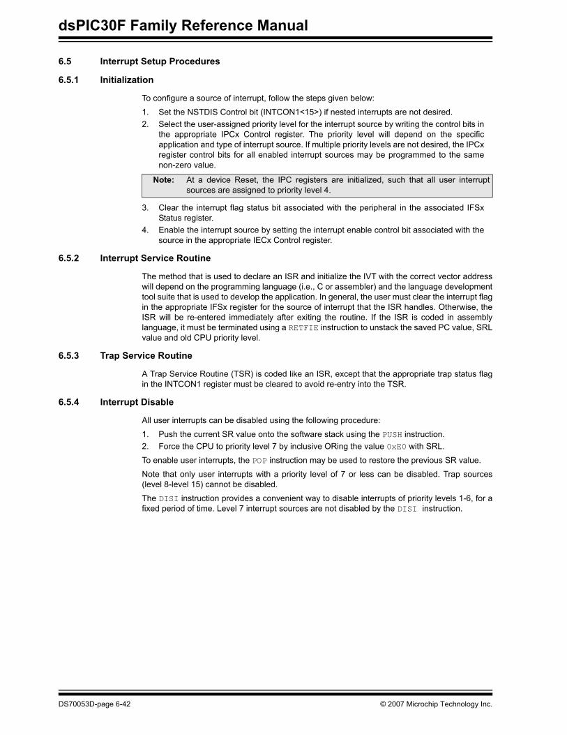
6.5 Interrupt Setup Procedures
6.5.1 Initialization
To configure a source of interrupt, follow the steps given below:
1. Set the NSTDIS Control bit (INTCON1<15>) if nested interrupts are not desired.2. Select the user-assigned priority level for the interrupt source by writing the control bits in
the appropriate IPCx Control register. The priority level will depend on the specificapplication and type of interrupt source. If multiple priority levels are not desired, the IPCxregister control bits for all enabled interrupt sources may be programmed to the samenon-zero value.
3. Clear the interrupt flag status bit associated with the peripheral in the associated IFSxStatus register.
4. Enable the interrupt source by setting the interrupt enable control bit associated with thesource in the appropriate IECx Control register.
6.5.2 Interrupt Service Routine
The method that is used to declare an ISR and initialize the IVT with the correct vector addresswill depend on the programming language (i.e., C or assembler) and the language developmenttool suite that is used to develop the application. In general, the user must clear the interrupt flagin the appropriate IFSx register for the source of interrupt that the ISR handles. Otherwise, theISR will be re-entered immediately after exiting the routine. If the ISR is coded in assemblylanguage, it must be terminated using a RETFIE instruction to unstack the saved PC value, SRLvalue and old CPU priority level.
6.5.3 Trap Service Routine
A Trap Service Routine (TSR) is coded like an ISR, except that the appropriate trap status flagin the INTCON1 register must be cleared to avoid re-entry into the TSR.
6.5.4 Interrupt Disable
All user interrupts can be disabled using the following procedure:
1. Push the current SR value onto the software stack using the PUSH instruction.2. Force the CPU to priority level 7 by inclusive ORing the value 0xE0 with SRL.
To enable user interrupts, the POP instruction may be used to restore the previous SR value.
Note that only user interrupts with a priority level of 7 or less can be disabled. Trap sources(level 8-level 15) cannot be disabled.
The DISI instruction provides a convenient way to disable interrupts of priority levels 1-6, for afixed period of time. Level 7 interrupt sources are not disabled by the DISI instruction.
Note: At a device Reset, the IPC registers are initialized, such that all user interruptsources are assigned to priority level 4.
DS70053D-page 6-42 © 2007 Microchip Technology Inc.
Section 6. InterruptsInterrupts 6
© 2007 M
icrochip Technology Inc.D
S70053D
-page 6-43
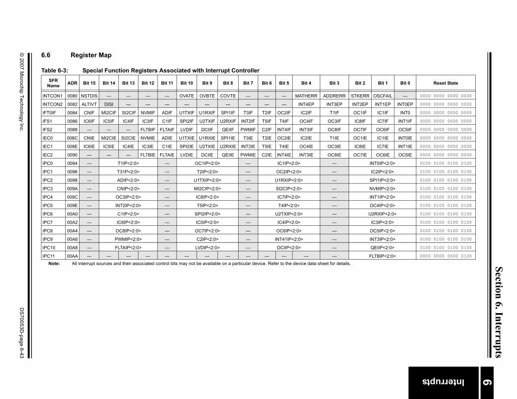
6.6
Ta
Bit 1 Bit 0 Reset State
IN R OSCFAIL — 0000 0000 0000 0000
IN P INT1EP INT0EP 0000 0000 0000 0000
IFT IC1IF INT0 0000 0000 0000 0000
IFS IC7IF INT1IF 0000 0000 0000 0000
IFS OC6IF OC5IF 0000 0000 0000 0000
IEC IC1IE INT0IE 0000 0000 0000 0000
IEC IC7IE INT1IE 0000 0000 0000 0000
IEC OC6IE OC5IE 0000 0000 0000 0000
IPC INT0IP<2:0> 0100 0100 0100 0100
IPC IC2IP<2:0> 0100 0100 0100 0100
IPC SPI1IP<2:0> 0100 0100 0100 0100
IPC NVMIP<2:0> 0100 0100 0100 0100
IPC INT1IP<2:0> 0100 0100 0100 0100
IPC OC4IP<2:0> 0100 0100 0100 0100
IPC U2RXIP<2:0> 0100 0100 0100 0100
IPC IC3IP<2:0> 0100 0100 0100 0100
IPC OC5IP<2:0> 0100 0100 0100 0100
IPC INT3IP<2:0> 0100 0100 0100 0100
IPC QEIIP<2:0> 0100 0100 0100 0100
IPC FLTBIP<2:0> 0000 0000 0000 0100
Register Map
ble 6-3: Special Function Registers Associated with Interrupt ControllerSFR
Name ADR Bit 15 Bit 14 Bit 13 Bit 12 Bit 11 Bit 10 Bit 9 Bit 8 Bit 7 Bit 6 Bit 5 Bit 4 Bit 3 Bit 2
TCON1 0080 NSTDIS — — — — OVATE OVBTE COVTE — — — MATHERR ADDRERR STKER
TCON2 0082 ALTIVT DISI — — — — — — — — — INT4EP INT3EP INT2E
0IF 0084 CNIF MI2CIF SI2CIF NVMIF ADIF U1TXIF U1RXIF SPI1IF T3IF T2IF OC2IF IC2IF T1IF OC1IF
1 0086 IC6IF IC5IF IC4IF IC3IF C1IF SPI2IF U2TXIF U2RXIF INT2IF T5IF T4IF OC4IF OC3IF IC8IF
2 0088 — — — FLTBIF FLTAIF LVDIF DCIIF QEIIF PWMIF C2IF INT4IF INT3IF OC8IF OC7IF
0 008C CNIE MI2CIE SI2CIE NVMIE ADIE U1TXIE U1RXIE SPI1IE T3IE T2IE OC2IE IC2IE T1IE OC1IE
1 008E IC6IE IC5IE IC4IE IC3IE C1IE SPI2IE U2TXIE U2RXIE INT2IE T5IE T4IE OC4IE OC3IE IC8IE
2 0090 — — — FLTBIE FLTAIE LVDIE DCIIE QEIIE PWMIE C2IE INT4IE INT3IE OC8IE OC7IE
0 0094 — T1IP<2:0> — OC1IP<2:0> — IC1IP<2:0> —
1 0096 — T31P<2:0> — T2IP<2:0> — OC2IP<2:0> —
2 0098 — ADIP<2:0> — U1TXIP<2:0> — U1RXIP<2:0> —
3 009A — CNIP<2:0> — MI2CIP<2:0> — SI2CIP<2:0> —
4 009C — OC3IP<2:0> — IC8IP<2:0> — IC7IP<2:0> —
5 009E — INT2IP<2:0> — T5IP<2:0> — T4IP<2:0> —
6 00A0 — C1IP<2:0> — SPI2IP<2:0> — U2TXIP<2:0> —
7 00A2 — IC6IP<2:0> — IC5IP<2:0> — IC4IP<2:0> —
8 00A4 — OC8IP<2:0> — OC7IP<2:0> — OC6IP<2:0> —
9 00A6 — PWMIP<2:0> — C2IP<2:0> — INT41IP<2:0> —
10 00A8 — FLTAIP<2:0> — LVDIP<2:0> — DCIIP<2:0> —
11 00AA — — — — — — — — — — — — —Note: All interrupt sources and their associated control bits may not be available on a particular device. Refer to the device data sheet for details.

dsPIC30F Family Reference Manual
6.7 Design Tips
Question 1: What happens when two sources of interrupt become pending at the sametime and have the same user-assigned priority level?
Answer: The interrupt source with the highest natural order priority will take precedence. Thenatural order priority is determined by the Interrupt Vector Table (IVT) address for that source.Interrupt sources with a smaller IVT address have a higher natural order priority.
Question 2: Can the DISI instruction be used to disable all sources of interrupt andtraps?
Answer: The DISI instruction does not disable traps or priority level 7 interrupt sources.However, the DISI instruction can be used as a convenient way to disable all interrupt sourcesif no priority level 7 interrupt sources are enabled in the user’s application.
DS70053D-page 6-44 © 2007 Microchip Technology Inc.

Section 6. InterruptsInterrupts
6
6.8 Related Application NotesThis section lists application notes that are related to this section of the manual. Theseapplication notes may not be written specifically for the dsPIC30F Product Family, but theconcepts are pertinent and could be used with modification and possible limitations. The currentapplication notes related to the Interrupts module are:
Title Application Note #No related application notes at this time.
Note: Please visit the Microchip web site (www.microchip.com) for additional ApplicationNotes and code examples for the dsPIC30F Family of devices.
© 2007 Microchip Technology Inc. DS70053D-page 6-45

dsPIC30F Family Reference Manual
6.9 Revision HistoryRevision A This is the initial released revision of this document.
Revision B This revision incorporates additional technical content for the dsPIC30F Interrupts module.
Revision CThis revision incorporates all known errata at the time of this document update.
Revision DThis revision includes minor changes to the document text and the addition of a note in 6.1.5“Interrupt Priority”.
DS70053D-page 6-46 © 2007 Microchip Technology Inc.