Embed Size (px)
Citation preview

C. R. Physique 12 (2011) 387–416
Contents lists available at ScienceDirect
Comptes Rendus Physique
www.sciencedirect.com
Article for the 50th anniversary of the invention of the LASER
Science and technology challenges in XXIst century opticalcommunications
Challenges scientifiques et technologiques des télécommunications optiques du XXIèmesiècle
E. Desurvire a,∗, C. Kazmierski b, F. Lelarge b, X. Marcadet b, André Scavennec b, F.A. Kish c,D.F. Welch c, R. Nagarajan c, C.H. Joyner c, R.P. Schneider Jr. c, S.W. Corzine c, M. Kato c,P.W. Evans c, M. Ziari c, A.G. Dentai c, J.L. Pleumeekers c, R. Muthiah c, S. Bigo d,M. Nakazawa e, D.J. Richardson f, F. Poletti f, M.N. Petrovich f, S.U. Alam f, W.H. Loh f,D.N. Payne f
a Thales Research & Technology, Physics Research Group, Campus de Polytechnique, 1, avenue Augustin Fresnel, 91767 Palaiseau cedex, Franceb Alcatel-Thales III-V Lab, joint laboratory of Alcatel-Lucent Bell Labs France and Thales Research & Technology, route de Nozay, 91460 Marcoussis, Francec Infinera Corporation, 1322 Bordeaux Drive, Sunnyvale, CA 94089, USAd Alcatel-Lucent, Bell Labs, Centre de Villarceaux, 91620 Nozay, Francee Tohoku University, Research Institute of Electrical Communication, Sendai, Japanf Optoelectronics Research Centre, University of Southampton, Southampton SO17 1BJ, UK
a r t i c l e i n f o a b s t r a c t
Article history:Received 8 April 2011Accepted after revision 8 April 2011
Keywords:Erbium-doped fibre amplifierModulation formatOptical telecommunicationsPhotonicsShannon limitWavelength-division multiplexing
Mots-clés :Amplificateur à fibre dopée à l’erbiumFormat de modulationPhotoniqueLimite de ShannonMultiplexage en longueur d’ondeTélécommunications optiques
The state of the art of XXIst century optical communication systems is reviewed throughthe associated technologies of laser sources, photo-receivers, integrated photonic circuits,optical fibres, and coherent modulation formats. Emphasis is put on current science andtechnology challenges to approach ultimate physical limits and to develop innovativesolutions allowing performance enhancement at minimal cost increase.
© 2011 Académie des sciences. Published by Elsevier Masson SAS. All rights reserved.
r é s u m é
Cette présentation passe en revue l’état de l’art des systèmes de télécommunicationsoptiques du XXIème siècle à travers les technologies des sources lasers, des photorécepteurs,des circuits photoniques intégrés, des fibres optiques, et des formats de modulationcohérents. L’accent y est placé sur les challenges scientifiques et technologiques posés parl’approche des limites physiques ultimes et par le développement de solutions innovantespermettant l’augmentation des performances au moindre coût.
© 2011 Académie des sciences. Published by Elsevier Masson SAS. All rights reserved.
* Corresponding author.E-mail addresses: [email protected] (E. Desurvire), [email protected] (C. Kazmierski), [email protected] (F.A. Kish),
[email protected] (S. Bigo), [email protected] (M. Nakazawa), [email protected] (D.J. Richardson).
1d
631-0705/$ – see front matter © 2011 Académie des sciences. Published by Elsevier Masson SAS. All rights reserved.oi:10.1016/j.crhy.2011.04.009

388 E. Desurvire et al. / C. R. Physique 12 (2011) 387–416
Nomenclature
A/D Analog-to-digitalADC Analog-to-digital converterAPD Avalanche photo-diodeASE Amplified spontaneous emissionASIC Application-specific integrated circuitAWG Arbitrary waveform generatorAWG Arrayed waveguide gratingBER Bit error rateBT British TelecomCAGR Compound annual growth rateCD Chromatic dispersionCMA Constant-modulus algorithmCVD Chemical vapour depositionCW Continuous laserCWA Chemical weapon agentDFB Distributed Feed-BackDGE Dynamic gain equaliserDGD Differential group delayDIRCM Directed counter-measureDM Dispersion managementDML Directly modulated laserDPSK Differential phase-shift keyingDVD Digital video diskE-PSCF Enhanced pure silica-core fibreEA Electro-absorptionEDFA Erbium-doped fibre amplifierEML Electro-absorption modulated laserFEC Forward Error correctionFIR Finite impulse responseFIT Failure in timeFM Frequency modulationFP Fabry–PérotFSK Frequency shift keyingHNL-DFF Highly-nonlinear dispersion-flattened fibreI-Q Cosine-sine (components)IC Integrated circuitICT Information and communication technologiesIDF Inverse dispersion fibreIF Intermediate frequencyIR InfraredISD Information spectral densityITU International Telecommunication UnionLASER Light amplification by stimulated emission of
radiationLD Laser diodeLO Local oscillatorMLFL Mode-locked fibre laserMLL Mode-locked laserMOCVD Metal-organic chemical vapour depositionNRZ Non-return to zero
O/E OptoelectronicOCM Optical counter-measureOEIC Optoelectronic integrated circuitOFDM Optical frequency-division multiplexingOFT Optical Fourier transformOFTC Optical Fourier transform circuitOML Optical Moore’s LawOOK On-Off keyingOPLL Optical phase-locked loopOSNR Optical signal-to-noise ratioOTDM Optical time division multiplexingP-DPSK Partial differential phase-shift keyingPBGF Photonic-bandgap fibrePC Polarisation controllerPIA Phase-insensitive amplifier/amplificationPIC Photonic integrated circuitPDM Polarisation division multiplexingPLL Phase-locked loopPM Polarisation multiplexingPMD Polarisation mode dispersionPMF Polarisation-maintaining fibrePOL-MUX Polarisation multiplexingPPG Pulse-pattern generatorPRBS Pseudo-random bit sequencePSA Phase-sensitive amplifier/amplificationPSK Phase shift keyingPSP Principal state of polarisationQAM Quadrature-amplitude modulationQCL Quantum cascade laserQD Quantum dot/dashQPSK Quadrature-phase-shift-keyingQW Quantum wellRE Rare earthRF Radio frequencyRT Room temperatureRZ Return-to-zeroS-QW Single quantum wellSAGM Separate absorption grading and multiplicationSMF Single-mode fibreSMSR Side-mode suppression ratioSMZ Symmetric Mach–ZehnderSNR Signal-to-noise ratioSSPM Self-phase modulationSMF Standard single-mode fibreTEC Thermal electric coolerTIC Toxic industrial chemicalVOA Variable optical attenuatorWDM Wavelength-Division MultiplexingWPE Wall plug efficiency

E. Desurvire et al. / C. R. Physique 12 (2011) 387–416 389
1. Introduction
1.1. Highlights on optical telecommunications history
The realisation by Corning Glass, in 1970, of the first low-loss fibres which had been predicted in 1966 by K.C. Kao andG. Hockham [1], and the parallel invention of semiconductor laser diodes and photo-detectors [2] may be seen as the twoparents of a newborn field, optical telecommunications. Compared to previous coaxial cable systems and free-space radiolinks, whether terrestrial or satellite, optical fibres offered an overwhelming, virtually “infinite” bandwith reservoir. Such a“bandwidth” concept means the capability to code signals and propagate them at virtually any data rate. This is becauseoptical carriers oscillate at 200,000 GHz frequencies, to compare with MHz–GHz radio communications. Furthermore, theultimate transparency of the fibre’s ultra-pure glass made it possible to transmit such signals over distances as long as100–150 km, with enough light photons at the fibre end to faithfully recover, regenerate or re-amplify the data.
To K.C. Kao and C.A. Hockham, such a level of achievement has been both a matter of vision and challenge. The visionwas that fibre waveguides could be used to transmit laser-light signals. The key innovation was to surround the fibre coreby a cladding of slightly lower refractive index, so as to trap the light rays by total internal reflection in the core. Throughappropriate waveguide design, light is further confined into a unique electro-magnetic propagation mode, hence the name:“single-mode” fibre, or SMF. The challenge was then to find the proper material with which to make the fibre. Glass, such asthat based on silica (of which sand is essentially composed), was the most transparent material known at the time. In theearly 1960s, the best silica glass could transmit light at 0.8 μm wavelength with 20% loss, or one decibel, per meter. Such aloss figure would make a 30 m-long fibre absorb 99.9% of the signal, meaning only 1/1000th would be transmitted, whichis wholly impractical from any engineering viewpoint! But in their 1966 reference, K.C. Kao and C.A. Hockham predictedthat the elimination of various glass impurities could lead to much more transparent materials, with an attenuation limitnear 20 dB/km, namely yielding 1/100th transmission over one kilometre of fibre. The quest for the “Holy Grail” was thenengaged. As we know, the historical 20 dB/km milestone was reached only four years later (1970); but the quest for anultimately-pure glass was not over yet. The following decade witnessed an even more spectacular domestication of fibreattenuation, as illustrated in Fig. 1. The lowest attenuation-coefficients loci in the light-transmission spectrum, would defineas many successive “transmission windows” for optical telecommunications, namely: 0.8 μm, 1.1 μm, 1.3 μm and finally,1.55 μm. Nowadays, optical fibres transmit 1.55 μm signals at a 1/10th to 1/100th levels of attenuation, but this time over50 to 100 kilometre spans! In parallel to these phenomenal developments, compact and efficient semiconductor laser chipsat 1.3 μm then 1.55 μm wavelength have been designed and qualified for efficiency, reliability, and yield, thus completing,with high-speed digital electronics, the basic optical telecommunications technology.
Since those heroic times, progress in the field has been running at a breathtaking pace, creating another “Moore’s Law”,as illustrated in Fig. 2. The figure shows optical-transmission performance achieved through successive technology stages(the “S-curves”) in terms of Capacity × Distance (bit km/s). This means the combined error-free transmission capacity(bit/s), times the distance (km). As a reference, a 1 Gbit/s system crossing the Pacific ocean (say 10,000 km) represents aC × D of 10,000 Gbit km/s, or 10 Terabit km/s (Tera = 1000 Giga). The figure highlights five generations in optical telecom-munications history. Overlooking the first two (based upon 0.8 μm, multi-mode fibre, and the 1.3 μm SMF), we reach outto the 1.5 μm transmission window, along with its improved dispersion-compensating fibre (DSF) design. By the mid-1980s,the corresponding C × D reaches its own GIGA limit, just as the coherent-system approach, for receiver sensitivity improve-ment. For that matter, coherent systems were seen not to make any difference with standard direct-detection systems, muchunlike twenty years after, as we shall see.
To progress any further, the stumbling stone remained fibre loss. Since the fibre transmission spans were, by the laws ofphysics, ultimately limited to 100–150 km, signals had to be electronically regenerated. This means converting the receivedlight signals back into electrical signals, amplifying them electrically, and then reconverting them back to light by means ofa complex optoelectronic device. For years on, this inescapable engineering fact represented a severe bottleneck to deployingoptical networks and to fully exploiting the otherwise enormous fibre transmission capability.
Such an obstacle was overcome by the optical fibre amplifier. The principle consists of lightly doping the core of a shortsegment of fibre with an atomic element such as the rare-earth erbium. The erbium dopant has the capability to storeenergy and to release it as the optical signals pass through the fibre core, in accordance with Einstein’s principle of stimu-lated emission, upon which the LASER is based. The energy release from the erbium atoms boost or re-amplify the signals,hence the name of the device, the Erbium-doped fibre amplifier, or EDFA. In order to excite the erbium atoms, one needsan auxiliary laser source, referred to as the pump. The early EDFAs were investigated around 1987–1988 by teams at theUniversity of Southampton and Bell Laboratories [3–5]. The great challenge faced by these teams and others, was to developa practical, efficient, and miniature pump source. Luckily, the same InGaAsP technology used in semiconductor laser diodes(LD) for optical telecommunications sources could be used for EDFA pumping once it had been redesigned to maximisepower efficiency,1 as demonstrated in 1989 by Nippon Telegraph & Telecommunications [3–5]. It is noteworthy that the two
1 From an engineering perspective, the EDFA is highly power-efficient. First, the 1.55 μm laser transition is 100% radiative, i.e. without parasitic thermal-phonon relaxation. Second, the pumping efficiency, which scales as the pump-to signal photon-energy ratio (or the inverse wavelength ratio) is 95.5% and63.2% for 1.48 μm and 980-nm pump wavelengths, respectively. Third, the semiconductor pump wall-plug efficiency (optical-to-electrical power ratio) is the

390 E. Desurvire et al. / C. R. Physique 12 (2011) 387–416
Fig. 1. Evolution though history of fibre attenuation vs. wavelength, showing four generations of transmission windows for fibre-optic communications, aslabelled by the lowest-loss wavelength: 0.8 μm, 1.1 μm, 1.3 μm and finally 1.55 μm wavelengths (after full elimination of the “OH peak” near 1.4 μm).
Fig. 2. Evolution through history of optical transmission-system performance, as expressed in capacity × distance (bit km/s), and according to successivetechnology generations. From left to right, the “S-curves” correspond to the following generations: 0.8 μm multi-mode fibre (open circles), 1.3 μm single-mode fibre (dark circles), 1.5 μm dispersion-shifted fibre (open circles), first coherent systems (dark circles), and EDFA-based systems (yellow circles/curve),with coherent multi-level formats (yellow circles/purple curve). From the time of early optical fibres (1970) to now, the capacity × distance performancehas been multiplied a billion-fold. The straight blue line, showing a heuristic tenfold performance increase every four years up to year 2000, correspondsto the optical Moore’s Law. (For interpretation of the references to colour in this figure, the reader is referred to the web version of this article.)
founding technologies of optical communications, namely the laser and the fibre, could be conjoined into the EDFA, a laser-pumped,doped-fibre amplifier.
The phenomenal EDFA impact in system performance is illustrated Fig. 2. To date, telecom history has entered its TERAand the PETA (1 PETA = 1000 TERA) performance eras. The relatively sudden and unexpected availability of practical,compact and efficient, LD-pumped EDFAs made it possible to periodically regenerate signals along optical fibre links, withoutany optoelectronic (O/E) regeneration obstacle through the line. A single fibre could from then on seamlessly transmit opticalsignals over any distance from 500–1000 km up to 12,000 km, which explains the observed exponential progress.
But the EDFA came out with another striking property. When deeply saturated with high input signal loads, electronicamplifiers cause signal distortion and nonlinear mixing. In contrast, the EDFA behaves as a truly linear device, at least atsignal bit rates of relevance. This is explained by the relatively slow dynamics of the amplifying medium (i.e. in the mil-lisecond scale). The early investigators rapidly identified the potential of the EDFA to re-amplify several signals at differentwavelengths simultaneously and without any mutual interference. Transmitting multiple signals in a single fibre in order to
highest possible for any lasers (typically well above 50%). Such advantageous properties are very important in the electrical power budget of EDFA-basedoptical communication systems, particularly in long-haul terrestrial (500–1000 km) or ultra-long-haul undersea (5000–12,000 km) applications. In the lastcase, terminal equipment in the class of 1 kV/1 A are capable to feed the entire system from the two continent ends. Depending upon the cable-systemhaul, EDFA regenerators are required every 50–70 km, the shortest spans applying to the longest. In terrestrial applications, the regenerative spans aretwice, i.e. 100–150 km. In specific undersea applications called “repeaterless systems”, the EDFAs are only placed at emission (booster) and reception(pre-amplifier) ends; in such a case, optical signals may propagate without in-line regeneration over fibre distances as long as 500 km.

E. Desurvire et al. / C. R. Physique 12 (2011) 387–416 391
enhance the system’s throughput capacity is referred to as wavelength-division multiplexing, or WDM. While the WDM ap-proach was impractical with previous O/E regeneration, overnight it became straightforward with the introduction of theEDFA. Indeed, the erbium atoms doped into the fibre core can amplify signals at practically any data rate, as limited by theterminal’s electronics. Together with the lack of inter-channel interference referred to above, thousands of billions of bitsfrom 100–200 WDM channels could be regenerated at once in the EDFA, with perfect integrity.
In order to achieve today’s system performance, however, the sole combination EDFA + WDM was hardly enough. Indeed,carrying such a huge amount of data over long (� 1000 km) or ultra-long fibre distances (� 10,000 km) is not at all thisstraightforward. This is because optical fibres exhibit a fair amount of nonlinearity, i.e. the refractive index becoming signal-power-dependent above a certain threshold. Fibre nonlinearity causes signal distortion, amplitude and phase noise, anddisastrous WDM channel interference. On the wake of the EDFA/WDM revolution, the history of optical communicationsessentially turns out being the matter of “domesticating” fibre nonlinearity, together with that of fibre dispersion (throughnovel fibre designs), in such a way to enable transport of more and more error-free data over longer distances. Back againto Fig. 2, where the last S-curve reveals key improvements such as dispersion management (DM), Er-amplifier “conventional”and “long” bands exploitation (C + L), forward error correction (FEC), Raman-amplification bandwidth upgrade (Raman), andpolarisation multiplexing (POL-MUX).
With all of the above incremental improvements, it has been possible to “pack” more and more data in the availablefibre bandwidth, namely the EDFA or EDFA/Raman-enhanced bandwidths. After the previous O/E bottleneck, “bandwidth”became limited once again, this time by the actual number of bits that could be packed into a given slide of spectrum, beit 100 GHz or 10 THz. What follows then is the stunning return to age-old coherent modulation/reception techniques. Theseallow signal formats capable of carrying several bit-per-second-per-Hertz, such that quadrature-phase-shift-keying (QPSK),a variant of the more general quadrature-amplitude modulation (QAM). For instance, 8-QAM packs three bits into a singleHertz.
As seen at the right of Fig. 2, the suite and combination of all the above-described techniques, from EDFA/WDM tocoherent, has led to the current PETA era, representing a billion-fold improvement in transmission capability since the inceptionof optical communications. It is also seen from the figure that the current S-curve dramatically departs from a heuristic“Optical Moore’s Law” (OML), representing a tenfold increase every four years, which was verified until about year 2000.Since then, the gap between the OML and actual performance is a thousand-fold. According to all expectations, anotherS-curve should be taking over in this PETA era, with the introduction of some disruptive concepts. The key question is whatthese could be about, and when such a disruption may take place, [6]. Another issue, of a most fundamental nature, is thatraised by Shannon’s information theory: how much error-free information may be transmitted through the “noisy opticalchannel”, anyway? The answer is provided by the most elegant Shannon–Hartley theorem [7], but the ultimate modulationformats and code systems remain yet to be discovered.
But is there any future need for more bandwidth anyway? From all operators, service providers and analysts, the answeris a solid and definitive YES! Optical fibres are now deployed worldwide across the land and along the seabed, forming anetwork of over one billion kilometres in length. Initially, the application was long-distance digital telephone and transactiondata. By year 2000, the traffic demand was overtaken by the forceful emergence of a revolutionary new service, the Internet.To date, the worldwide Internet traffic represents 50 EXAbytes per year, a fifty-fold increase since 2000. The prefix “exa”stands for one billion billion, or a factor 1018. This amounts to the information contained in 50,000 Libraries of Congress,representing the information in 150 billion books being transmitted every day over the Internet. Another way to look at it isto consider that 10 Tbit/s, the capacity of today’s global optical communications, corresponds to the full transmission of 250digital video-disks (DVD), per second. By year 2009, the optical fibre production and installation produced worldwide wasover 160 M km/year. This number converts into 5.2 km/s, fifteen times the speed of sound! By year 2015, at a conservative+17% growth rate, the Earth fibre plant will amount 3 billion kilometres, or over 75,000 times its circumference. It istrue that for this generation and others to come, we live in a “connected world”. Little known from the vast majority ofend-users, the ubiquitous Internet connectivity rests upon this EDFA/WDM web of glass fibres.
The looming issue of a future “bandwidth exhaustion”, as described earlier in [6], remains beyond the scope of thisarticle. Here, the idea is rather to provide a flavor of the different technologies being harnessed towards a full exploitationof the currently-available fibre/components bandwidth. Such an activity domain is far to have reached and final conclusion,and this point is important to highlight.
1.2. About this article
This article is a contribution to the celebration of the 50th anniversary of the invention of the LASER, and also a specialhomage to the 2009 Nobel Prize, Charles K. Kao, for the invention of fibre optics. Our mandate has been to describe,to a broad scientific community, the impact of the LASER in fibre-optics, to highlight the “state of the art” of opticalcommunications, and to share a “view of the future”. In 2003 and 2008, similar reviews were published in two previousissues of this journal [8,9]. However, this one is very special, not only due to this celebration context, but also becauseoptical telecommunications seem to have reached an historical turning point, as highlighted above. The task of furtherdescribing the scientific and technical issues, and the remaining challenges with respect to future bandwidth demand, hasbeen entrusted to five leading contributor teams, covering the following topical areas:

392 E. Desurvire et al. / C. R. Physique 12 (2011) 387–416
Fig. 3. Self-thermally compensated 10 Gbit/s 1.55 μm laser: Simulated (lines) and experimental (dots) laser threshold, power (at 100 mA) and characteristictemperature T0 for +25 nm DFB detuning.
– optical components (by C. Kazmierski et al.), in Section 2;– integrated photonic circuits (by F. Kish et al.), in Section 3;– long-haul terabit/s transmission (by S. Bigo), in Section 4;– advanced modulation formats (by M. Nakazawa) in Section 5;– next-generation fibre optics (by D. Richardson et al.), in Section 6.
Each of these sections are self-introductory and can be read independently, with a concern from the authors to clarify attheir best the scientific concepts and the technology challenges, for this journal’s readership. A joint conclusion summarisesthe key issues and questions now facing “modern” optical communications.
2. LASER-based fast photonic sources
2.1. Introduction
Directly modulated Distributed Feed-Back (DFB) single wavelength lasers remain one of the pillars of low-cost transmis-sion equipment for Black&White and Wavelength Division Multiplexing (WDM) applications, owing to their compactness,high output power and low cost. Their fabrication simplicity is a way to further decrease the transmitter cost and to addressthe new 10 Gbit/s markets of Fibre-To-The-Home access converging with metropolitan networks. An important effort wasmade recently to increase the operating temperature of DFB in order to decrease, or eventually suppress, thermoelectriccooler consumption in uncooled lowest cost assembling [10] especially for 1.3 μm DFBs, reaching today industrial maturity.However, high temperature 1.55 μm DFBs are also required in order to cover low cost and consumption, large spectral rangeWDM applications. They are more difficult to obtain due to a larger thermal dependence of material gain at longer wave-lengths [11]. Recently, a breakthrough has been attained by the conjunction of high gain AlGaInAs/InP S-QW active materialsystem and strong positive detuning of the DFB peak from the gain peak [12]; this conjunction produces an efficient SelfThermal Compensation of the laser threshold and power. It decreases the power variation at the laser output and allowsoperating at higher temperatures without changing the bias current (Fig. 3). Such lasers were able to link 25 km standardSingle Mode Fibre (SMF) without amplification or dispersion compensation at the industry standard 10 Gbit/s data rate upto 90 ◦C and 100 km SMF up to 80 ◦C with the help of electronic equalisation circuits for the first time [12,13]. Furtherresearch is now carried out to enhance their speed to 25 Gbit/s and then, maybe, up to 40 Gbit/s.
The speed limits of the directly modulated lasers coming from carrier-photon dynamics can be overcome by an ex-ternal modulation using material gap modifications induced by a strong electric field. Not involving carriers, electro-opticor electro-absorption modulation effects intrinsically behave with sub-picosecond dynamics. However, the speed of actualcomponents is today technology limited due to their parasitic Resistance*Capacitance (RC) frequency roll-off. They have aspecial economic interest when integrated with lasers in simple Photonic Integrated Circuits (PIC). While PICs and OEICs(OptoElectronic Integrated Circuits) have been explored for more than 20 years, only a limited number of very simple oneshas met any commercial success so far (e.g. wavelength tunable Distributed Bragg Reflector laser, Electroabsorption Mod-ulated Lasers: EML), so that optoelectronic front ends are mainly simple Transmitting or Receiving Optical Sub-Assembliescontaining a laser (or electro-optic modulator) or a photo-detector. Recently, by using an enhanced electro-absorption Al-GaInAs/InP S-QW active material in a high modulation sensitivity EML PIC, a new step has been reached in terms of speed,with a 60 GHz bandwidth and 86–100 Gbit/s data rate demonstration (Fig. 4) [14]. These results allow energy and costefficient short-reach and interconnect applications, but also open a way to more complex PICs able to handle much largerdata rates due to the very low size (50 μm) of electro-absorption modulators.
Due to the constant telecom traffic increase, a capacity growth by a factor of 30 to 100 will be required by the endof the next decade. Following an evolutionary path based on the simple introduction of additional channels will just not
E. Desurvire et al. / C. R. Physique 12 (2011) 387–416 393
Fig. 4. 86 Gbit/s data rate of a low-voltage InP HBT driver co-packaged with high modulation efficiency EML.
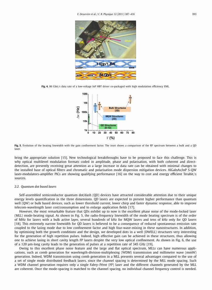
Fig. 5. Evolution of the beating linewidth with the gain confinement factor. The inset shows a comparison of the RF spectrum between a bulk and a QDlaser.
bring the appropriate solution [15]. New technological breakthroughs have to be proposed to face this challenge. This iswhy optical multilevel modulation formats coded in amplitude, phase and polarisation, with both coherent and direct-detection, are presently receiving great attention as a large increase in data rate can be obtained with minimal changes tothe installed base of optical filters and chromatic and polarisation mode dispersion mitigation devices. AlGaInAs/InP S-QWlaser-modulators-amplifier PICs are showing qualifying performance [16] on the way to cost and energy efficient Terabit/ssources.
2.2. Quantum dot based lasers
Self-assembled semiconductor quantum dot/dash (QD) devices have attracted considerable attention due to their uniqueenergy levels quantification in the three dimensions. QD lasers are expected to present higher performance than quantumwell (QW) or bulk based devices, such as lower threshold current, lower chirp and faster dynamic response, able to improvetelecom-wavelength laser cost/consumption and to enlarge application fields [17].
However, the most remarkable feature that QDs exhibit up to now is the excellent phase noise of the mode-locked laser(MLL) mode-beating signal. As shown in Fig. 5, the radio-frequency linewidth of the mode beating spectrum is of the orderof MHz for lasers with a bulk active layer, several hundreds of kHz for MQW lasers and tens of kHz only for QD lasers[18]. This extremely narrow linewidth for QD lasers is believed to be a consequence of reduced spontaneous emission ratecoupled to the lasing mode due to low confinement factor and high four-wave-mixing in these nanostructures. In addition,by optimising both the growth conditions and the design, we developed dots in a well (DWELL) structures very interestingfor the generation of high repetition pulses. Indeed, high effective gain can be achieved in these structures, thus allowingone to achieve lasing in short cavity length FP lasers despite the very low optical confinement. As shown in Fig. 6, the useof a 120 μm-long cavity leads to the generation of pulses at a repetition rate of 345 GHz [19].
Owing to this excellent phase noise feature and the large and flat optical spectrum, MLLs can have numerous appli-cations, such as comb generation for wavelength-division-multiplexing (WDM) transmission and millimetre wave (mmW)generation. Indeed, WDM transmission using comb generation in a MLL presents several advantages compared to the use ofa set of single mode distributed feedback lasers, since the channel spacing is determined by the MLL mode spacing. Sucha WDM channel generation requires only a single Fabry–Pérot (FP) laser and the different channels generated by the MLLare coherent. Once the mode-spacing is matched to the channel spacing, no individual channel frequency control is needed.

394 E. Desurvire et al. / C. R. Physique 12 (2011) 387–416
Fig. 6. Optical spectrum (top) and autocorrelation trace (bottom) for 120 μm-long QD laser demonstrating a repetition rate of 345 GHz.
Fig. 7. Transmission Electron Microscopy image of a QCL structure. Insert: Typical conduction band diagram of a QCL.
We demonstrated recently the comb generation in the 1.5 μm window and error-free transmission over 50 km SMF of 8WDM ITU channels at 10 Gbit/s with a channel spacing of 100 GHz for WDM transmission in a QD-MLL [20]. Owing tothe reasonable relative intensity noise level, a penalty of only 1.5 dB is achieved compared to the use of an external cavityCW laser. Such a good performance allows one to consider such a solution in an integrated WDM transceiver. The very lowradio-frequency linewidth of QD-MLLs makes these devices very attractive for high frequency signal generation for radiotransmission or radar applications [21,22]. As an illustration, we have integrated the 54.8 GHz MLL into a dual loop cou-pled optoelectronic oscillator using suitable fibre length values. The phase-noise reduction is more than 30 dB at an offsetfrequency of 50 kHz giving a phase noise below −82 dBc/Hz, at this offset frequency. Moreover, we demonstrated that thegenerated 60 GHz waves using a QD-MLL can be successfully used for wireless transmission through external modulationor direct modulation. For instance, a frequency up-conversion from 6 GHz to 60 GHz of an OFDM signal was realised bydirectly modulating a FP MLL whose mode-beating frequency is 54 GHz. This results in a simple up-conversion schemewith improved conversion efficiency; it also provides means to transport and to distribute the 60 GHz radio signal usingradio-over-fibre transmission.
Such a remarkable performance paves the way for the penetration of QD technology into the ICT market. Further materialoptimisation are still on-going in order, for instance, to reduce the inhomogeneous broadening and the polarisation sensitiv-ity of QDs, which result from their strain-driven nucleation process, and to identify the more relevant telecom applicationsfor such nanostructures based devices.
2.3. Quantum cascade lasers
The quest to produce powerful light sources covering the Mid-Infra Red (Mid-IR) 3–12 μm wavelength range for defence,security and environmental applications is still very strong. Several technological options are today available or under de-velopment. Among the technologies available, semiconductor sources appear to be the best long-term option since they areinvolving only one electrical-optical conversion that can be very efficient. Furthermore, semiconductor lasers have a poten-tial for extreme compactness, high lifetime, high reliability and low cost. Quantum Cascade Lasers (QCLs) are today the onlysemiconductor laser sources operating at room temperature in pulsed or continuous modes over the 4–10 μm wavelengthrange.
The quantum cascade laser is a semiconductor light source based on resonant tunnelling and optical transitions betweenquantised conduction band states [23], see Fig. 7. Instead of being classically fixed by the physical properties of the con-stituent materials, the lasing mechanism mainly depends on the layer sequence forming the heterostructure, giving a unique

E. Desurvire et al. / C. R. Physique 12 (2011) 387–416 395
Fig. 8. DFB QCL spectra of devices available at Alcatel-Thales III-V Lab. The corresponding molecules for gas sensing applications are indicated.
flexibility for designing devices emitting in a wide spectral range up to the THz region (3.5–160 μm). At present, the bestperformance is reached at wavelengths between 4–10 μm.
Two main QCL families can be defined, according to their applications: high power Mid-IR QCLs for Optical Counter Mea-sure (OCM) for sensor jamming or dazzling and tunable single mode Mid-IR QCLs for explosives, drugs, Chemical WeaponAgents (CWAs), see Fig. 8, Toxic Industrial Chemicals (TICs) and pollutant agent spectroscopy. Free-space optical communi-cations could be a possible application which will also take advantage of the Mid-IR atmospheric transparency windows.
QCLs were invented 15 years ago and have now reached a certain degree of maturity. However, the business of quantumcascade lasers is still in its infancy. There are today only two commercial companies in Europe which are really able tofabricate and deliver quantum cascade lasers: a Swiss SME called Alpes Laser founded in 1998 by Jérôme Faist, one of theco-inventors of QCLs and Alcatel-Thales III-V Lab.
Single-frequency operation of the laser is required for spectroscopy application. It is usually achieved by introducing adistributed feedback (DFB) structure into the QCL active region in order to favour a particular mode. Pulsed mode operationof these devices at Room Temperature (RT), mounted on a Thermal Electric Cooler (TEC) is now easily achieved. On theother hand, Continuous Wave (CW) RT operation lasers on TEC are still more lab devices than commercial products [24].Fabry–Pérot QCLs operating in CW at RT in the 4–5 μm range with an output power of 500 mW and a beam quality factorof M2 ∼ 1.2 (diffraction limited) in the fast and slow axes are currently available to be evaluated in systems for protectingaircrafts from shoulder-fired missiles. Maximum single-ended continuous-wave optical power levels of 3 W at 4.6 μm atRT were obtained recently by US labs. This power level corresponds to maximum wall plug efficiency (WPE) of 13% for amulti-mode transverse beam [25].
The main limiting point to reach today high-power quantum cascade laser sources is their low WPE which is currentlyinvestigated by several research groups. The theoretical limit (∼ 30%) is an open problem, but it exceeds by far the currentlyachieved world record (∼ 16%) and commercial device performance (∼ 5%). Besides the improvement of the intrinsic perfor-mances of the single QCL element, integrated chip-level approaches will constitute the innovative solutions for the foreseenapplications. As an example, the hybrid evanescent-wave integration of QCL on silicon (or Ge/Si) waveguides is a promisingtechnique to demonstrate infrared spectrometer-on-a-chip [26]. Concerning a future DIRCM system where cost and powerscaling will be important, an extraordinarily high power beam with a single transverse mode could be obtained by beamcombining of several phase locked QCLs on the same chip.
Although the main applications of QCLs are focusing today on chemical detection and sensor jamming, their physicalproperties are very attractive for long-term evolutionary step in energy efficient telecommunications with growing speedand capacity requirements. For example, QCLs may solve spectral overcrowd in wireless communications, potentially pro-viding terahertz bandwidth and energy efficiency improvement due to directional targeting of reduced size cells. Also, theprogress of new materials such as GaN and related compounds may bring a revolution in fibre telecom laser speed workingat 1.3–1.5 μm, no longer limited by photon–electron resonance [27].
2.4. Photo-detectors
Imaging, photovoltaics and optical fibre transmission have been the main drivers in the evolution of photo-detectorsduring the last decades, in particular in the visible and near infrared part of the spectrum. In the area of optical fibretransmission, this evolution followed three main directions, while keeping the conversion quantum efficiency close to one:
– increase of the wavelength of interest, from 0.85 μm to 1.5 μm;– tremendous increase in the data rates;– improvement in sensitivity.

396 E. Desurvire et al. / C. R. Physique 12 (2011) 387–416
Fig. 9. Evolution of InGaAs/InP photo-diode structures towards thinner absorption region, and increased bandwidth, from the front illumination scheme(left) to back illumination (middle) and finally side illumination (right). Simultaneous reduction of the junction area results in lower junction capacitance,and overall larger optoelectronic bandwidth.
One family of photo-detectors established itself as the most efficient one: the pn or pin photo-diode, in which the absorp-tion region is mainly located in the junction depletion region where the high electric field separates photo-carriers. Whilethe first photo-diodes for telecom were made in silicon, providing good absorption at 0.85 μm wavelength, a compoundsemiconductor, InGaAs, lattice-matched to InP was used for the longer wavelengths: owing to its absorption characteristics,since this material provides excellent responsivity up to 1.6 μm wavelength, together with a large bandwidth resulting fromthe short associated absorption length (1 to 2 μm).
As the bandwidth requested by growing data rates was increasing, the photo-diode structure itself kept evolving thanksin particular to the use of heterojunctions:
– at first, transparency of the InP substrate (and of the front p-layer) was instrumental in allowing a back illuminationscheme rather than the conventional front illumination. This new scheme allowed one to reduce the InGaAs absorptionlayer thickness by a factor of two, while reducing simultaneously the junction area (both transit time and charging timeare then lowered);
– a second major step is associated with the double heterostructure scheme [28], similar to a semiconductor laser, witha very thin absorbing core (very short transit time) compatible with very large optoelectronic bandwidths (>100 GHz).Reaching a good coupling efficiency between the cleaved or lensed fibre and the photo-diode required an importantdevelopment. Edge illuminated photo-diodes are now available, with a large acceptance input multi-mode waveguideand an evanescently coupled thin absorption junction [29,30]. Such photo-diodes offer a figure of merit (bandwidth ×responsivity) of 50 GHz A/W at 1.5 μm (see Fig. 9).
After propagation, the optical signal power is most often quite weak, and can hardly be separated from noise. In order toincrease the sensitivity, several solutions have been investigated: (i) integration with high sensitivity electronic amplifiers,such as the Transimpedance Amplifiers (TIAs); this actually motivated many developments in the area of Optoelectronic Inte-grated Circuits (OEICs); (ii) association with optical pre-amplifiers; this technique is widely used in WDM receivers in whichseveral photo-receivers can share a same pre-amplifier; (iii) avalanche photo-detector with internal photo-current multipli-cation. In this device, impact ionisation is activated by applying a large electric field. Through this process, photo-carriersare multiplied and the output signal as well. First avalanche photo-diodes (APDs), made from silicon, exhibited almostideal characteristics: bandwidth of a few hundreds MHz, large enough for the intended data rates (34–140 Mb/s), usefulavalanche gain of about 100 without bandwidth reduction, and low excess noise. Such characteristics, resulting from thevery attractive ionisation properties of Si and from a structure design fully benefiting from these properties (the so-calledpπpπn structure), have not been met with materials suited for longer wavelengths, whether Ge or InP related compounds.However, high performance APDs have been fabricated in this latter material system, owing to two main innovations:
– a design suited to avalanche operation, with Separate Absorption Grading and Multiplication regions (SAGM): whileabsorption occurs in InGaAs, multiplication takes place in a wider bandgap, and lower dark current, material; an inter-mediate region, providing some bandgap grading, prevents carriers trapping;
– an avalanche material with acceptable properties. InP was the choice material for the first APDs. However its poorionisation characteristics resulted in a factor of merit (gain × bandwidth) of 60–80 GHz, too low for 10 Gbit/s applica-tions. With a more favourable ionisation coefficients ratio and a factor of merit in the 140–160 GHz, AlInAs offered anacceptable solution for these data rates, providing a sensitivity close to −30 dBm at 10 Gbit/s [31].
Photo-detectors keep evolving, adjusting to the market needs. For instance, the trend in long haul transmission is torely on spectrally efficient modulation schemes, possibly with coherent detection. Such schemes require large bandwidth,high linearity photo-diodes, a challenge for photo-diodes with a decreasing active region and higher associated carrierdensity. Power consumption in routers and switches is also a problem, which can benefit from an improved photo-receiversensitivity, a challenge for OptoElectronic Integration, whether on InP or Si.

E. Desurvire et al. / C. R. Physique 12 (2011) 387–416 397
Fig. 10. Scaling of the data capacity/chip for InP-based transmitter chips utilised in commercial telecommunications networks. All data points are fordeployed commercial networks except the 500 Gbit/s chip that is in development.
2.5. Conclusions
Discrete or small-scale PIC transmitting and receiving components, especially those based on indium phosphide technol-ogy, have become an integrated part of the optical fibre communication industry. The unique ability of the InP materialsfamily to efficiently generate laser emission in silica fibre transmission windows makes the associated technology the bestcandidate for larger scale integration of all optical functions. However, improvement of discrete component characteristicsfor higher performance in speed, chip size, electro-optical conversion efficiency and high temperature operation remains amajor quest. In the coming decade these devices will be facing the challenge of supporting a growing transmission capac-ity demand, while offering the increased requested wavelength agility and, simultaneously, a low environmental cost (lowenergy and material consumptions).
InP-laser based technical progress increasingly coincides with a larger societal impact: from connecting people, thistechnology now addresses emerging applications and markets like security, medical imaging, pollution sensing, etc. Onewould see there a seed for next technological revolutions better accounting for limited Earth’s resource constraints.
3. Monolithic LASER integration into large-scale photonic circuits
3.1. Introduction
The discovery of the laser 50 years ago [32] was followed two years later by the realisation of a semiconductor version[33–36], despite the fact that considerable new physics were needed to be discovered to realise this form of laser (using p–njunctions to inject current in a direct gap semiconductor to obtain stimulated emission). Since its discovery, the semicon-ductor laser has made tremendous advances, including (but not limited to) the development of: heterojunction lasers andcw operation [37,38], the realisation quantum-well lasers [39], and the development of distributed feedback (DFB) lasers[40,41]. This progression, combined with the development of long-wavelength InP-based semiconductor lasers in the low-loss spectrum of the optical fibre [42], enabled the deployment of semiconductor lasers to enable transmission in opticalfibre networks.
Since the first laser was deployed an optical fibre network in 1984, there has been a steady scaling of increased capacityper chip as shown in Fig. 10. Discrete devices (first LEDs and later directly modulated lasers (DMLs)) were deployed duringthe first ∼ 15 years of building optical networks. In order to continue to scale both the data capacity and performance,the development of photonic integrated circuits (PICs) was required [43]. The first transmitter devices deployed in opticalfibre networks began with small-scale integration and consisted of electroabsorption modulated lasers [44]. This enabledthe realisation of devices with a capacity up to 10 Gbit/s per chip. The next significant progression occurred with thedevelopment of large-scale PICs where over 50 devices were integrated onto a monolithic chip to realise a 100 Gbit/stransmitter chip (10 channels × 10 Gbit/s) [45]. This advance represented an order of magnitude increase in data capacityper chip compared to existing commercial devices and utilised a multi-wavelength array of ten tunable DFB lasers (alignedto an ITU grid). Next generation large-scale PIC technologies (not yet deployed) are being developed with capacities of� 500 Gbit/s (5 × 100 Gbit/s and above [46]), and integrate over 400 functions onto a single chip.
The scaling of electronic integrated circuits has progressed at an exponential rate as predicted by Moore [47] since theirinvention in 1959 [48,49]. This is in contrast to photonic integrated circuits, where the pace of integration has been dwarfedrelative to electronic ICs. This dramatic difference is mainly due to the inability of the value delivered by a PIC to outweighthe cost of integrating optical elements monolithically onto a chip.

398 E. Desurvire et al. / C. R. Physique 12 (2011) 387–416
Fig. 11. Schematic of the OOK large-scale PIC transmitter chip. The commercially deployed devices have 10 channels whereas 40 channels have beendemonstrated on research devices. The SOA elements on the second generation chip enable the PICs to be capable of being deployed in ULH and submarineapplications.
Circa 2001, numerous developments in the III-V semiconductor and optoelectronics field corroborated to help enable thedevelopment of commercial large-scale photonic integrated circuits. These included the development of high-quality, low-defect density 50–100 mm diameter InP substrates, the development of metal-organic chemical vapour deposition (MOCVD)as a viable means for the growth of high-precision lasers and optoelectronics devices, the development of precision dry-etchtechnologies for low-loss waveguides and reliable devices, and fine line lithography. This “tool kit” allowed the constructionof a PIC fabrication capability that was designed from the outset for manufacturability. Large-scale PICs could then bedeveloped in such a facility using a similar methodology as electronic ICs, wherein designers are given a fixed (limited) toolset (e.g., design rules) to design within, resulting in a manufacturable (cost-effective) device. This methodology was used atInfinera Corporation, simultaneously combining the large-scale PIC capability with the design and development of networkproducts that maximised the value delivered by large-scale PICs. This provided, for the first time, a viable commercial sourceand value proposition for such devices.
3.2. 100 Gbit/s transmitter PICs
A schematic diagram of the architecture of commercial large-scale transmitter PICs is shown in Fig. 11. These devices con-sist of a 10-channel array with each channel consisting of tunable laser integrated with an electroabsorption (EA) modulator,a variable optical attenuator (VOA), and a power monitor. Each of the 10 channels is then multiplexed into a monolithi-cally integrated arrayed waveguide grating (AWG) which provides a single output for fibre-coupling in a hermetic package.The devices are hybrid packaged with a 10-channel analog ASIC EA modulator driver chip and are Telecordia qualified toGR-468 standards. A second generation 100 Gbit/s large-scale PIC transmitter capable of ultra long-haul/submarine reaches(> 600 km) [50,51] has been also developed and deployed which adds per-channel semiconductor optical amplifiers andsubstitutes power monitors for the VOAs.
The 100 Gbit/s transmitter PICs consists of 10 channels arranged on a 200 GHz grid in the C-band (the system performsdownstream multiplexing of similar transmitters to achieve a system-level 25 GHz grid). The spectrum of the lasers fromsuch a transmitter PIC is shown in Fig. 12. The lasers are tuned to within < ±2 GHz of the ITU grid over life and exhibitan SMSR > 40 dB. In addition, superimposed on the laser spectra of Fig. 12 is the AWG multiplexer transmission function.This shows that the AWG pass-bands and laser frequencies are very well-aligned, resulting in minimal power loss frommisalignment.
Large-scale 100 Gbit/s PIC transmitters were first commercially deployed in 2004, with devices now operating for over46,000 hours in the field Over 400 M field hours have been accumulated on commercially deployed devices (PIC Transmittermodules) corresponding to < 2.5 FIT, which is comparable to the discrete pump lasers [52], albeit on PICs with over 50monolithically integrated elements.
3.3. 500 Gbit/s coherent transmitter PICs
The large-scale PIC transmitter platform has shown to be capable of scaling beyond the currently deployed commercial100 Gbit/s devices. Specifically, devices have been demonstrated extended the channel count of the commercial devices

E. Desurvire et al. / C. R. Physique 12 (2011) 387–416 399
Fig. 12. Superposition of the 10 channel DFB spectrum with the AWG multiplexer transmission function for 10-channel large-scale PIC transmitter.
Fig. 13. Schematic of the 10-channel, 500 Gbit/s pol-mixed QPK transmitter PIC. All elements are monolithically integrated on a single chip except thepolarisation rotator (Rot) and beam combiner PBC which are off-chip.
(in Fig. 10) to 40 channels as well as simultaneously increasing the speed of the EA modulators from 10 Gbit/s [53] to40 Gbit/s [54] with > 200 elements integrated on single chip.
For bit rates beyond 10 Gbit/s, phase-based modulation formats offer distinct advantages in link and network per-formance, including 2–4× gains in spectral efficiency and better optical signal-to-noise ratio (OSNR) tolerance [55].High-capacity large-scale PIC transmitters capable of polarisation-multiplexed quadrature phase-shift keying PM-QPSK at400 Gbit/s and 500 Gbit/s have been developed [46,55,56]. A schematic of such a chip which integrates over 400 elementsper chip is shown in Fig. 13. The device consists of 5 channels, operating at 100 Gbit/s channel where each channel consistsof 2 carriers (wavelengths) [56]. This dual-carrier format has been shown to enable superior performance at lower baudrates than a single-carrier (wavelength approach) [57]. Each channel consists of a DFB (with back power monitor) whichfeeds two distinct nested I-Q Mach–Zehnder modulators that are then multiplexed into two distinct AWGs. The outputfrom one of the AWGs is polarisation rotated (off-chip) and then combined (off-chip) with the other output to produce apolarisation-multiplexed architecture.
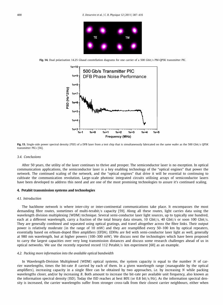
Fig. 14 shows the exemplary constellation diagram for one of the 10 carriers that are output from the 500 Gbit/stransmitter PIC in a packaged module. The input data streams are generated using two independent but synchronisedpattern generators operating at 14.25 Gbit/s, with the input data consisting of two delayed PRBS 215 − 1 patterns. Theoutput of the transmitter PIC is characterised using a custom coherent receiver which includes a 50 Gs/s high-speed realtimesampling scope and proprietary signal processing. The other carriers operate with similar performance across the entire PIC.
Laser linewidth (phase noise) is a critical parameter for the successful high-performance operation of phase-modulatedsystems and PICs. Accordingly, we have developed lasers with narrow linewidth integrated into the phase-modulated PICs.An example of the power spectral density (PSD) of a laser fabricated on the same wafer as the 500 Gbit/s transmitter PIC isshown in Fig. 15 [58]. The inferred laser linewidth from this data is ∼ 300 KHz and is sufficient for meeting the performancerequired of long-haul and submarine networks for 500 Gbit/s PIC applications.
400 E. Desurvire et al. / C. R. Physique 12 (2011) 387–416
Fig. 14. Dual polarisation 14.25 Gbaud constellation diagrams for one carrier of a 500 Gbit/s PM-QPSK transmitter PIC.
Fig. 15. Single-side power spectral density (PSD) of a DFB laser from a test chip that is simultaneously fabricated on the same wafer as the 500 Gbit/s QPSKtransmitter PICs [56].
3.4. Conclusions
After 50 years, the utility of the laser continues to thrive and prosper. The semiconductor laser is no exception. In opticalcommunication applications, the semiconductor laser is a key enabling technology of the “optical engines” that power thenetwork. The continued scaling of the network, and the “optical engines” that drive it will be essential to continuing tocultivate the communication revolution. Large-scale photonic integrated circuits utilising arrays of semiconductor lasershave been developed to address this need and are one of the most promising technologies to assure it’s continued scaling.
4. Petabit transmission systems and technologies
4.1. Introduction
The backbone network is where inter-city or inter-continental communications take place. It encompasses the mostdemanding fibre routes, sometimes of multi-terabit/s capacity [59]. Along all these routes, light carries data using thewavelength division multiplexing (WDM) technique. Several semi-conductor laser light sources, up to typically one hundred,each at a different wavelength, carry a fraction of the total binary data stream, 10 Gbit/s, 40 Gbit/s or soon 100 Gbit/s.They are generally combined and separated using optical gratings, and travel altogether across the fibre links. Their outputpower is relatively moderate (in the range of 10 mW) and they are reamplified every 50–100 km by optical repeaters,essentially based on erbium-doped fibre amplifiers (EFDA). EDFAs are fed with semi-conductor laser light as well, generallyat 980 nm wavelength, but at higher powers (100–300 mW). We discuss next the technologies which have been proposedto carry the largest capacities over very long transmission distances and discuss some research challenges ahead of us inoptical networks. We use the recently reported record 112 Petabit/s km experiment [60] as an example.
4.2. Packing more information into the available optical bandwidth
In Wavelength-Division Multiplexed (WDM) optical systems, the system capacity is equal to the number N of car-rier wavelengths, times the bit-rate B carried by each of them. In a given wavelength range (manageable by the opticalamplifiers), increasing capacity in a single fibre can be obtained by two approaches, i.e. by increasing N while packingwavelengths closer, and/or by increasing B . Both amount to increase the bit-rate per available unit frequency, also known asthe information spectral density (ISD). Today the ISD reaches at best 80% (or 0.8 bit/s/Hz). As the information spectral den-sity is increased, the carrier wavelengths suffer from stronger cross-talk from their closest carrier neighbours, either when

E. Desurvire et al. / C. R. Physique 12 (2011) 387–416 401
Fig. 16. Computed optical spectra (all at same scale) showing various approaches to fill an amplifier bandwidth. The constellation diagram depicts thepossible modulation states taken by the complex electric field of light at the same energy per bit for all diagrams.
Fig. 17. Schematic of a coherent-detection receiver (left), as compared to direct-detection receivers (right)
multiplexing (combining carrier wavelengths) or demultiplexing (separating carrier wavelengths), or during fibre propaga-tion, unless disruptive approaches are used. Coherent optical solutions have now been adopted as the most promising. Thesesolutions are just starting to provoke to a radical change in the design of optical networks, with possible implications asvast as that following the introduction of the EDFA in the 1990s.
Containing the spectral width of each wavelength carrier is the most straightforward remedy against increasing cross-talk. For each carrier, the incoming bits are encoded into a stream of successive symbols, at a rate called symbol rate. Intoday’s optical systems, symbols can take only two states, e.g. “1” or “0”, and hence the symbol rate matches the bit-rate, thesymbols are encoded by varying the intensity of light (light ON or light OFF) according to the widespread non-return to zero(NRZ) format, or by varying the phase (0 or π ) according to the differential Phase-Shift Keying format. However, the spectralwidth about each wavelength carrier is approximately twice the symbol rate (e.g. 80 GHz at 40 GSymbol/s). It can betruncated with a narrow optical filter [61] as with Partial-DPSK (PDPSK) [62], but to some extent only. A more efficient wayfor increasing the bit-rate per carrier wavelength, without affecting the spectral width, is to increase the possible numberof modulation states per symbols beyond two (see Fig. 16). One of the most interesting modulation formats would consistin allowing symbols to take four phase states, to make Quadrature Phase-Shift Keying (QPSK). By employing polarisationdivision multiplexing (PDM), i.e. by encoding two different QPSK data streams along the two polarisation components oflight, a bit rate per carrier wavelength four times as large as with two states per symbol can be obtained over unchangedspectral bandwidth. This has opened the way to carrier wavelengths modulated at 100 Gbit/s (25 GSymbol/s) over thesame 50 GHz frequency grid as at 10 Gbit/s, but with tenfold increase of information density at 200% (2 bit/s/Hz).
4.3. Coherent detection
Recovering the signal multiple symbol states is the challenge that a coherent receiver can solve. Such a receiver isinherently more complex than conventional direct-detection (see Fig. 17). The contrast is naturally greater when compared

402 E. Desurvire et al. / C. R. Physique 12 (2011) 387–416
Fig. 18. Schematic of 112 Petabit/s km experiment (left) Q2 factors of the 155 WDM channels (right).
with receivers for NRZ, than with receivers involving differential detection for Phase-Shift Keyed formats like DPSK andDifferential QPSK. Coherent detection relies on the beating onto photo-diodes of the signal beam with the beam of a cwlaser called the local oscillator, normally a twin of the signal laser used to generate the optical data at the transmitter. Bothbeams are combined into a coherent mixer, which generates four interference beams from the four output ports. The mixeris designed such that, from one port to the next, the relative phase between signal and local oscillator has been rotatedby another 90◦ . Ports 1 & 3 and 2 & 4 are feeding two sets of balanced photo-diodes (Fig. 17). To achieve polarisationdemultiplexing, two coherent mixers should be operated in parallel. Their photo-currents are sampled before further digitalprocessing. In contrast to conventional photo-receivers for NRZ format which only provide the signal power out of a simplephoto-diode, coherent receivers provide the signal amplitude, phase, and state of polarisation.
Powerful algorithms convert the digitised waveforms from the four photo-diodes back to bit streams. Additionally, theavailability of the full signal characteristics opens tremendous opportunities against all the impairments that limit theachievable transmission distance in today’s fibre systems. The tolerance to noise, to Polarisation Mode Dispersion [63], tochromatic dispersion [59], and to a large cascade of reconfigurable nodes distributed along the link has already been ex-tended to ranges unseen with other techniques. However, the algorithms must process a very high flow of data in real time,e.g. 1 Terabit/s per chip. Challenging though the implementation seems, coherent detection has already been experimentedin commercial product for 100 Gbit/s applications since mid-2010.
In the experiment described next, the chip is emulated with a free-running oscilloscope, while the Analog-to-Digital Con-verters (ADC) of Fig. 17, right, are replaced by its sampling heads. This oscilloscope operates at a rate of 50 GSamples/s andcan store 0.5 million samples at once, simultaneously from all four heads. These samples are used to convert optical databack to electrical data streams with digital signal processing in successive steps: re-sampling at twice the symbol rate, possi-ble dispersion compensation through Finite Impulse Response (FIR) filter, digital clock recovery, polarisation demultiplexingthrough 5-tap adaptive filtering based on the Constant Modulus Algorithm (CMA) [64], carrier-phase estimation using theViterbi and Viterbi algorithm [65] and finally symbol identification. After symbol identification, the received electrical bitstreams are compared to the original from the transmitter for error counting.
4.4. 112 Petabit/s km experiment
Recent research has shown that the full potential of coherent detection can only be revealed with its association withalternative technologies, not used in today’s 10 Gbit/s networks. The aforementioned multi-level modulation formats andPDM are two technologies which belong to this category. We shall now use the example of the first experiment with acapacity times distance product in excess of 100 Petabit/s km [60], to discuss other technologies that hold big promiseswhen associated with coherent detection. In this experiment 155 lasers are modulated at 100 Gbit/s and transmitted over7200 km, as when 400 DVDs per second need to be sent across the ocean via a single optical fibre.
The transmitter is schematized in Fig. 18. It involves 155 distributed feedback (DFB) lasers spaced by 50 GHz, rangingfrom 1531.51 nm to 1562.64 nm in the C-band and from 1571.24 nm to 1602.74 nm in the L-band. The even and oddchannels of each band are combined into two spectrally-interleaved wavelength combs. Both combs are modulated inde-pendently into separate QPSK modulators, fed with 215 1 bit-long sequences at 28 Gbit/s, emulating 7% Forward-ErrorCorrection (FEC) and protocol overheads. The output from each modulator is split along two polarisation-maintaining fibre(PMF) paths in a 3 dB coupler. The QPSK data along one path are delayed by hundreds of symbols into a PMF, before be-ing polarisation-multiplexed with the QPSK data along the other path through a polarisation beam combiner. This schemeproduces PDM-QPSK channels at 112 Gbit/s. The odd and even channels are then spectrally interleaved through a 50 GHzinterleaver, and boosted into a C-band or an L-band EDFA, whichever applies. The output of C and L EDFA boosters are com-bined thanks to a C/L multiplexer and injected into the recirculating loop. The loop consists of eight 90-km-long spans ofEnhanced Pure Silica Core Fibre (E-PSCF), characterised by 110 μm2 effective area, 0.168 dB/km average loss, < 0.1 ps/
√km
polarisation mode dispersion. No dispersion-compensating fibre is used here, in contrast to all experiments performed at10 Gbit/s. Fibre loss is compensated for by hybrid Raman–erbium optical repeaters. Each repeater incorporates a C-band
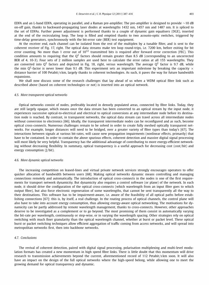
E. Desurvire et al. / C. R. Physique 12 (2011) 387–416 403
EDFA and an L-band EDFA, operating in parallel, and a Raman pre-amplifier. The pre-amplifier is designed to provide ∼10 dBon-off gain, thanks to backward-propagating laser diodes at wavelengths 1432 nm, 1457 nm and 1487 nm. It is spliced tothe set of EDFAs. Further power adjustment is performed thanks to a couple of dynamic gain equalisers (DGE), insertedat the end of the recirculating loop. The loop is filled and emptied thanks to two acousto-optic switches, triggered bytime-delay generators, synchronously with the bit-error rate (BER) test equipment.
At the receiver end, each channel can be isolated from the rest of the multiplex by a tunable filter, and is sent to thecoherent receiver of Fig. 17, right. The optical data streams make ten loop round-trips, i.e. 7200 km, before exiting for biterror counting. No more than 1 error out of 1012 transmitted bits is required after forward error correction (FEC). Thiscondition amounts to requiring that the Q2 factors should remain greater than 8.5 dB (corresponding to an uncorrectedBER of 4. 10-3). Four sets of 2 million samples are used here to calculate the error ratios at all 155 wavelengths. Theyare converted into Q2 factors and depicted in Fig. 18, right, versus wavelength. The average Q2 factor is 9.7 dB, whilethe min Q2-factor is never lower than 9.1 dB. This experiment sets an important milestone by breaking the capacity ×distance barrier of 100 Petabit/s km, largely thanks to coherent technologies. As such, it paves the way for future bandwidthexpansions.
We shall now discuss some of the research challenges that lay ahead of us when a WDM optical fibre link such asdescribed above (based on coherent technologies or not) is inserted into an optical network.
4.5. More transparent optical networks
Optical networks consist of nodes, preferably located in densely populated areas, connected by fibre links. Today, theyare still largely opaque, which means once the data stream has been converted to an optical stream by the input node, itexperiences successive optical-to-electrical and electrical to optical conversions at any intermediate node before its destina-tion node is reached. By contrast, in transparent networks, the optical data stream can travel across all intermediate nodeswithout conversion to electronics [66]. Ideally, the transparent intermediate nodes can be reconfigured and as such, becomeoptical cross-connects. Numerous challenges remain to be solved in order to create fully meshed optically transparent net-works. For example, longer distances will need to be bridged, over a greater variety of fibre types than today’s [67]. Theinteractions between signals at various bit-rates, will cause new propagation impairments (nonlinear effects, primarily) thathave to be contained. In order to contain the above spurious effects, coherent detection and massive digital signal processingwill most likely be very helpful. Transparency has the additional advantage of contributing to more energy-efficient network-ing without decreasing flexibility. In summary, optical transparency is a useful approach for decreasing cost (cost/bit) andenergy consumption (J/bit).
4.6. More dynamic optical networks
The increasing competition on leased-lines and virtual private network services strongly encourages operators to offerquicker allocation of bandwidth between users [68]. Making optical networks dynamic means controlling and managingconnections remotely and automatically. The introduction of optical cross-connects in the nodes is one of the first require-ments for transport network dynamicity. But dynamicity also requires a control software (or plane) of the network. In eachnode, it should drive the configuration of the optical cross-connects (which wavelength from an input fibre goes to whichoutput fibre), but also force electronic regeneration of some wavelengths, that cannot be sent transparently all the way totheir destinations. This software has to be impairment-aware, i.e. aware of the feasibility of all optical paths before estab-lishing connections [67]: this is, by itself, a real challenge. In the routing process of optical channels, the control plane willalso have to take into account energy consumption, thus allowing energy-aware optical networking. The motivations for dy-namicity can be partly addressed by remote wavelength management, thanks to cross-connects. However, other approachesdeserve to be investigated as a complement or to go beyond. The most promising of them consist in automatically varyingthe bit-rate per wavelength, continuously or step-wise, or in varying the wavelength spacing. Other strategies rely on opticalswitching with much finer granularity than the optical wavelength channel, whether at burst or packet level. These opticalburst or packet switching techniques allow efficient aggregation of traffic coming from access networks, and will spread intometropolitan networks first, then into backbone networks.
4.7. Conclusions
The revival of coherent detection, paired with digital signal processing, polarisation multiplexing and multi-level modu-lation formats has created a new momentum in high speed fibre links. There is little doubt that this momentum will driveresearch to transmission achievements beyond the current, aforementioned record of 112 Petabit/s km soon. It will alsohave an impact on the design of the full optical networks where the high-speed belong, while allowing one to meet thegrowing demand for optical transparency and dynamic.

404 E. Desurvire et al. / C. R. Physique 12 (2011) 387–416
Fig. 19. Recent experimental demonstrations on ultrahigh-speed OTDM transmission.
5. New frontiers in optical communications through multi-level coherent transmission
5.1. Introduction
To cope with the rapid growth of Internet traffic on a global scale, intensive efforts have been made to expand thecapacity of optical backbone networks. Recent trends in optical communication research can be divided mainly into twocategories. One is ultrahigh-speed transmission using ultrashort pulses, in which optical time division multiplexing (OTDM)is adopted to increase the bit rate per wavelength channel that exceeds the limit of electrical signal processing [69]. This isthe driving force behind attempts to realise an ultrahigh-speed optical network with a simple configuration, large flexibil-ity, and low power consumption, in which the complexity of wavelength routing at the switching nodes can be alleviatedthrough the need for fewer wavelength channels. The other trend is ultrahigh spectral density coherent transmission em-ploying multi-level modulation formats, whose aim is to expand the capacity of WDM transmission systems within a finitetransmission bandwidth [70,71]. In particular, quadrature amplitude modulation (QAM) is one of the most spectrally effi-cient modulation formats [72]. This technique is also important with a view to enhancing the tolerance to dispersion andpolarisation-mode dispersion (PMD) as well as to reduce the power consumption, as it enables us to realise a high-speedsystem with low speed devices.
In the first part of this section, we describe ultrahigh-speed OTDM transmission using the time-domain optical Fouriertransformation (OFT) technique. By employing OFT, 640 Gbit/s/channel single-polarisation DPSK transmission over 525 kmwas successfully demonstrated. In the latter part of this section, we describe a 256 QAM coherent optical transmission.64 Gbit/s (polarisation-multiplexed 4 Gsymbol/s, 256 QAM) data were successfully transmitted over 160 km with a 5.4 GHzoptical bandwidth, which corresponds to a spectral efficiency of more than 11 bit/s/Hz in a single channel.
5.2. Ultrahigh-speed OTDM transmission
Single-channel transmission beyond 1 Tbit/s is expected to be the technological driving force for constructingnext-generation ultrahigh-capacity optical transport networks such as terabit Ethernet. The first Tbit/s/ch transmissionexperiment was reported in 2000, in which a 1.28 Tbit/s polarisation-multiplexed OOK signal (640 Gbaud) was transmittedover 70 km [73]. Since then, attempts have been made to extend the transmission distance by adopting advanced modula-tion formats such as DPSK and DQPSK as shown in Fig. 19. By adopting DQPSK, polarisation-multiplexed 2.56 Tbit/s-160 kmtransmission has been demonstrated [74]. In these experiments, the symbol rate is 640 Gbaud. Since the pulse interval ina 640 Gbaud transmission is only 1.5 ps, such a high-speed transmission requires sub-picosecond pulses and therefore thesystem performance becomes vulnerable not only to chromatic dispersion (CD) and PMD but also to higher-order CD andPMD. This has limited the maximum transmission distance to 100–200 km.
Recently, we proposed a time-domain OFT technique [75] to cope with such transmission impairments. Time-domain OFT,in which the spectral profile is converted into a waveform in the time domain, makes it possible to eliminate the signaldistortions that result from linear transmission impairments in optical fibres, such as jitter, dispersion slope, higher-orderPMD, and time-varying perturbations. Here we present a single-polarisation 640 Gbit/s DPSK transmission over 525 kmusing the time-domain OFT technique, which is the longest transmission distance at a symbol rate of 640 Gbaud yet reported[76]. The OFT technique is successfully applied to a 640 Gbit/s DPSK signal, in which the strong chirp required for the OFTof a sub-picosecond pulse is realised with a phase modulator operated in a round-trip configuration.
The experimental setup for a 640 Gbit/s-525 km DPSK transmission is shown in Fig. 20. As an optical pulse source,we used a 40 GHz mode-locked fibre laser (MLFL) that generates a 2.0 ps pulse train at 1540 nm via mode-hop-freeoperation with an etalon installed in the cavity. To obtain the sub-picosecond pulse train required for 640 Gbit/s, weemployed external pulse compression based on spectral broadening using self-phase modulation (SPM) in a fibre with

E. Desurvire et al. / C. R. Physique 12 (2011) 387–416 405
Fig. 20. Experimental setup for a 640 Gbit/s-525 km DPSK transmission.
normal dispersion. The MLFL output pulse was amplified to 20.5 dBm and launched into a 2 km highly-nonlinear dispersion-flattened fibre (HNL-DFF) with a dispersion of −0.2 ps/nm/km, a dispersion slope of 0.002 ps/nm2/km and a nonlinearcoefficient γ = 5 W−1 km−1. After chirp compensation with a single-mode fibre (SMF), the pulse was compressed to 600 fs.
The compressed pulse was DPSK modulated with a 40 Gbit/s, 215 − 1 PRBS, where the pulse pattern generator (PPG)was synchronised to a 40 GHz clock that was extracted after the pulse compression. The DPSK signal was then opti-cally multiplexed to 640 Gbit/s with a single polarisation using an optical delay-line multiplexer, and launched into a525 km transmission fibre. The fibre link consisted of seven 75 km spans of dispersion-managed fibre composed of stan-dard single-mode fibre (SMF) and inverse dispersion fibre (IDF), which compensate for the dispersion and dispersion slopesimultaneously. The total dispersion and dispersion slope were precisely compensated with a short piece of SMF at the endof the transmission link. The average DGD was 1.2 ps, which is almost the same as the bit interval. To mitigate the first-order PMD, the polarisation state of the 640 Gbit/s input signal was optimised to match the principal state of polarisation(PSP) of the 525 km fibre link with a polarisation controller (PC). The fibre loss was compensated at each span by using anEDFA. An optimal average input power to each span of +12 dBm was chosen to minimise OSNR degradation and nonlinearimpairments. The pulse width after transmission estimated from an autocorrelation measurement varied between 630 and730 fs when measured over a long period. The pulse broadening and its long-term variation are due to time-dependentsecond-order PMD, which induces time-varying polarisation-dependent CD.
On the receiver side, the 640 Gbit/s OTDM signal was demultiplexed to 40 Gbit/s with an all-optical semiconductorsymmetric Mach–Zehnder (SMZ) switch [77], in which a 40 GHz MLFL emitting a 720 fs pulse operated by FM mode-locking was used as a control pulse source. The control pulse wavelength was set at 1561 nm. The MLFL was PLL-operatedwith a 40 GHz clock extracted from the 640 Gbit/s data using an electro-optical PLL clock recovery unit [78]. The opticalpower of the data and control pulse were set at 15 and 12 dBm, respectively. The polarisation state was adjusted with anautomatic PC. At the SMZ output, the demultiplexed signal was separated from the control pulse with 15 nm optical filters,in which the pulse width was broadened to 1.1 ps.
The demultiplexed DPSK signal was then launched into an optical Fourier transform circuit (OFTC). OFT can be realisedwith linear chirp with a chirp rate K followed by a dispersion medium where D = β2L that satisfies K = 1/D . To realisethe strong chirp required for OFT for a sub-picosecond pulse, we adopted a phase modulator operated with a round-tripconfiguration. The optical pulse is first launched into the modulator in the forward direction, and phase-modulated bythe RF signal travelling in the same direction. The optical pulse is then reflected and launched into the modulator in thebackward direction, where the pulse is phase-modulated by the backward-travelling RF signal. This allows us to obtain achirp twice as large as that obtained in an unidirectional phase modulator. We obtained a modulation depth of M = 3.6π ,corresponding to a chirp rate K = Mω2
m = 0.71 ps−2 at ωm = 2π × 40 GHz. The demultiplexed 40 Gbit/s DPSK signal wasfinally converted to an OOK signal with a one-bit delay interferometer (DI), and the bit error rate (BER) was measured afterdetection with a balanced photo-detector (PD).

406 E. Desurvire et al. / C. R. Physique 12 (2011) 387–416
Fig. 21. BER characteristics for 640 Gbit/s-525 km transmission.
Fig. 22. Recent transmission experiments with high spectral efficiency.
The BER characteristics of the 640 Gbit/s-525 km transmission for the best OTDM channel are shown in Fig. 21. WhenOFT was not employed there was an error floor in the BER performance, and the best BER was of the order of 10−8 to 10−9
and varied with time, as a result of the time-dependent higher-order PMD. On the other hand, when OFT was employed,error-free performance with a BER of below 10−9 was achieved with a power penalty of only 2 dB. The insert in Fig. 21shows the BER for all the OTDM tributaries measured with a received power of −16 dBm. The performance variation amongdifferent tributaries is attributed to intersymbol interference induced at the overlapping tails between adjacent pulses. A BERimprovement of more than one digit was realised with OFT, and the stability against time-varying perturbations such asPMD and coherent crosstalk between adjacent pulses was also improved. The obtained BER performance was sufficientlybelow the standard FEC threshold (2 × 10⁻³) for error-free operation.
5.3. Ultra-multilevel QAM coherent transmission
Coherent quadrature amplitude modulation (QAM) has attracted much attention with a view to increasing the spec-tral efficiency toward the Shannon limit. QAM is a modulation format that combines two carriers whose amplitudes aremodulated independently with the same optical frequency and whose phases are 90 degrees apart. These carriers are calledin-phase carriers (I) and quadrature-phase carriers (Q). 2N QAM signal processes N bits in a single channel, so it has N timesspectral efficiency compared with OOK (On-off-keying). The ultimate spectral efficiency is given by the Shannon limit2:
C
W= log2
(1 + Eb
N0
C
W
),
which is known as the Shannon–Hartley theorem [79]. The spectral efficiency of M-QAM approaches closer to the Shannonlimit than other advanced modulation formats such as PSK or FSK, as the QAM multiplicity M increases.
Recent transmission experiments with high spectral efficiency are shown in Fig. 22. A 10 × 112 Gbit/s polarisation-multiplexed (Pol-Mux) 16 QAM transmission was demonstrated with a spectral efficiency of 6.2 bit/s/Hz [80], and an
2 C [bit/s] is the channel capacity, W [Hz] is the bandwidth, Eb [J] and N0 [W/Hz] are the bit energy and noise, respectively.

E. Desurvire et al. / C. R. Physique 12 (2011) 387–416 407
Fig. 23. Experimental setup for 4 Gsymbol/s, 256 QAM transmission.
8 × 65.1 Gbit/s Pol-Mux, orthogonal frequency division multiplexing (OFDM) transmission with a spectral efficiency of7.0 bit/s/Hz was realised by using a sub-carrier modulation with 32 QAM [81]. To increase the spectral efficiency further,it is important to increase the multiplicity of the modulation level with sufficient SNR and IF frequency stability. Here wedescribe a 256 QAM coherent optical transmission with a Pol-Mux, 4 Gsymbol/s scheme over a 160 km standard single-mode fibre (SSMF) [82]. In this scheme, 64 Gbit/s data were transmitted with an optical bandwidth of 5.4 GHz.
The transmission setup is shown in Fig. 23. As a coherent light source, we employed a C2H2 frequency-stabilised fibrelaser [83], whose linewidth is 4 kHz and the frequency stability is 1.3 × 10⁻¹¹. The coherent light is QAM modulated withan IQ modulator, where the beam is modulated with a 4 Gsymbol/s, 256 QAM baseband signal generated by an arbitrarywaveform generator (AWG) running at 8 Gsample/s. We adopt a Nyquist filter with a roll-off factor of 0.35 at the AWGusing a piece of software [84] that enables us to reduce the bandwidth of the QAM signal to 5.4 GHz. After the modulation,the QAM signal is coupled with a pilot tone signal whose frequency is 10 GHz down-shifted against the data signal.
After the transmission, the QAM signal is homodyne-detected with a local oscillator (LO) to convert the QAM data intoa baseband signal. Here we employed an optical phase-locked loop (OPLL) technique to lock the optical phase betweenLO and QAM signal using the transmitted pilot tone, in which a high-speed free-running fibre laser is used as an LO. Inthe coherent receiver, the LO output is divided with a 90-deg phase shift each other and coupled with the QAM signal ina 90-deg optical hybrid circuit so that the cosine (I) and sine (Q) components are obtained after balanced detection. Thephase noise of the detected signal was as low as 0.3 deg, which is sufficiently small for demodulating a 256 QAM signal.Finally they are A/D converted and demodulated into a binary sequence in the DSP. Because of the software demodulation,this transmission system operates in an off-line condition.
The BER performance for the Pol-Mux, 4 Gsymbol/s, 256 QAM transmission is shown in Fig. 24. Here, the maximumdata length for demodulation was limited to 4096 symbols owing to the DSP memory size, which corresponds to a BERlimit of up to 3.1 × 10⁻⁵. In the back-to-back result, the received optical power at BER = 2 × 10⁻³ was P rec = −32.0 dBm,which corresponds to OSNR = P rec/nsphν�ν = 28.6 dB and Eb/N0 = OSNR(�ν/R) = 20.9 dB, where �ν is the detectionbandwidth of the optical signal and R is the data rate per polarisation. This value is close to the theoretical limit ofEb/N0 = 18.7 dB for 256 QAM [85]. This 2.2 dB difference may be attributed to the imperfect implementation of suchhardware as the AWG and the IQ modulator.
The power penalty at a BER of 1 × 10⁻³ was approximately 5.3 dB for both polarisations, but both sets of polarisationdata achieved a BER lower than the FEC limit of 2 ×10⁻³. Figs. 24(b) and 24(c) show constellation maps for the back-to-backcondition and after a 160 km transmission, respectively, at a received power of −21 dBm. Almost the same constellation wasobtained for parallel polarisation. As a result, 64 Gbit/s data were transmitted over 160 km under the FEC threshold withan optical bandwidth of 5.4 GHz, which indicates the possibility of realising a spectral efficiency as high as 11.8 bit/s/Hz

408 E. Desurvire et al. / C. R. Physique 12 (2011) 387–416
Fig. 24. Experimental results of 4 Gsymbol/s, 256 QAM transmission over 160 km. (a) BER characteristics, (b) and (c) constellations (4096 × 4 symbols)before and after 160 km transmission, respectively.
in a multi-channel transmission even when taking account of the 7% FEC overhead. An error-free transmission with a QAMas high as 256 levels requires an increase in the SNR at the transmitter and the receiver, a narrow band optical filter toremove amplified spontaneous emission (ASE) noise, and a large core fibre to reduce the fibre nonlinearity.
5.4. Conclusions
Two emerging optical transmission technologies, i.e. ultrahigh-speed OTDM transmission and coherent QAM transmission,were described. As regards the ultrahigh-speed transmission, we have adopted a time-domain OFT technique for improvingthe tolerance to higher-order PMD and demonstrated 640 Gbit/s/channel-525 km DPSK transmission. By combining this ap-proach with polarisation multiplexing and DQPSK modulation, we can expect to achieve a long-haul transmission as fast as2.56 Tbit/s/channel. As regards the coherent transmission, 256 QAM transmission was realised with a frequency-stabilisedfibre laser and an optical PLL technique, which indicates the possibility of spectral efficiency as high as 11 bit/s/Hz. Thesetechnologies play important roles for realising advanced high-speed optical backbone networks and ultra-efficient, largecapacity access networks.
6. Fibre technology for next generation networks
6.1. Introduction
Driven by society’s ever increasing data capacity demands, it is clear that the next generation of telecommunicationnetworks will be radically different from previous implementations; as we have seen in previous sections, multilevel coher-ent transmission and powerful digital signal processing will be deployed to maximise cable capacity. However, whilst thesedevelopments are welcome, they will only delay an inevitable “capacity crunch” as we exhaust the capacity of conventionalsingle mode fibre. Put simply, once these techniques are deployed over the coming years and the capacity of current trans-mission line technology is reached we will only be able to increase network capacity by lighting additional fibres – a farfrom attractive solution from an economic perspective. With a Compound Annual Growth Rate (CAGR) of over 40% [86], this

E. Desurvire et al. / C. R. Physique 12 (2011) 387–416 409
only delays a total capacity exhaust by a few years before new cable deployments are required (presumably at 40% of theinstalled base per annum using current fibres). However, the proximity of extensive deployment of new cables in the nextdecade (2020–2030) provides a unique opportunity to re-examine our choice of transmission fibre in the hope of findinga dramatic increase in per-fibre capacity. It is therefore clear that radical innovation in the basic internet infrastructure(i.e. transmission fibres and amplifiers) is now urgently required. Moreover, the technology will need to be commercialisedrapidly if we are to avoid this potential capacity crunch.
Unsurprisingly perhaps, many of the key issues to be faced in developing the next generation of fibres for telecommu-nication (e.g. nonlinearity, mode-control, and damage effects) are also critical in the context of high power fibre lasers.Consequently, we anticipate that much of the work done in this field, which has led to power scaling of fibre lasers fromthe 100 W to the 10 kW regime over the past decade, may be leveraged to good effect as we look to further capacity scaleour networks.
6.2. Enhancing the fibre capacity
In order to increase the capacity of a single optical fibre cable one can pursue a number of options either separately orpreferably in combination:
(1) Reduce the loss and nonlinearity of the transmission line. In order to maximise the data carrying capacity of a fibre itis necessary to operate with as high a signal spectral efficiency (and corresponding OSNR) as possible before the onset ofthe nonlinear impairments that ultimately compromise performance [87]. The reduction of nonlinearity and attenuation arethus primary targets for next generation transmission fibres. The incorporation of some form of signal regeneration can alsobe gainfully employed to help reduce the impact of nonlinearity and provide access to higher spectral efficiencies [88].
(2) Increase the number of separate information channels carried within the fibre using some form of spatial division multiplex-ing to increase the data capacity per unit cross sectional area of the fibre. Different forms of spatial division multiplexingcan be adopted, either within the same core (multi-mode transmission) or within the same fibre (multi-core transmission).
(3) Extend the usable spectral bandwidth beyond the C + L band as currently used – this requires the development both ofa transmission fibre with a suitably low-loss transmission window and an associated low-noise optical amplifier technology.
Clearly, in applying any new technique it is necessary to be mindful from the outset both of the optical power handlingand mechanical properties of the fibres and the associated overall electrical power requirements. In the following sectionsvarious technical options to realise the above targets are reviewed.
6.3. Transmission fibres with reduced loss and nonlinearity
6.3.1. Lower-loss silica fibresTo date, the lowest loss reported for a silica fibre, obtained with a pure silica core, is 0.148 dB/km [89]. This is very
close to the theoretical minimum for such a glass, meaning that there is very little scope for further improvement. Theminimum loss is determined by the levels of Rayleigh scattering and the proximity of the infrared absorption edge withinthe core glass. The level of Rayleigh scattering can be reduced by lowering the fictive temperature of the core glass –which is extremely high in silica – hence the 2000 ◦C processing temperature [90]. One possible way to reduce the Rayleighscattering is therefore to lower the melting temperature of the glass, which can be done by suitable doping of silica. Forexample, in [91], it was predicted that a 20–30% loss reduction down to the 0.11 dB/km level should be achievable usinga P2O5-F-silica based core. Practical realisation of such a fibre will require chemical vapour deposition (CVD) techniques toensure ultra-high purity and the search for a thermally compatible cladding material with acceptable loss and environmentalstability.
6.3.2. Non-silica fibresOwing to its excellent material processing characteristics and low optical loss, silica is an almost ideal fibre material.
However, there are a range of materials, most notably fluoride glasses, which potentially offer substantially lower intrin-sic losses than silica [92]. Indeed, the theoretical minimum loss of several fluoride glasses is predicted to be as low as0.03 dB/km at wavelengths around 2.5 μm. Significant research programs ran around the world until the early 1990s thatattempted to draw fibres with a lower loss than silica and significant progress was made with losses as low as 0.65 dB/kmreported by researchers at BT Research Laboratories [93]. With the development of the erbium doped fibre Amplifier (EDFA)and the difficulty of working with fluoride glasses (which are both hygroscopic and tend to produce fragile fibre) this workwas stopped in the early 1990s. However, with a looming capacity crunch and with the significant advances made in ma-terial purification and gas phase deposition in the past 20 years, it may be time to revisit this topic and to undertakefundamental materials/glass studies and fibre drawing trials to re-assess the prospects of this approach.
6.3.3. Photonic bandgap fibresHollow-core Photonic Band Gap Fibres (PBGFs) represent a technology that could potentially yield major benefits in terms
of both loss and nonlinearity. PBGFs comprise an array of longitudinal wavelength-sized holes periodically arranged in thecladding to form a photonic bandgap in the transverse plane of the fibre, and an air-filled hollow core in which light isconstrained to propagate over a tailorable spectral range [94]. The sub-percent fraction of optical power guided in the glass

410 E. Desurvire et al. / C. R. Physique 12 (2011) 387–416
Fig. 25. Top – various SEM images of PBGFs with different core sizes and associated fundamental mode images. Bottom – fundamental mode loss versuswavelength for different core designs showing the expected loss improvements due to better technological approaches to fibre manufacture and furtherscaling of the core size.
matrix means that Rayleigh scattering, the dominant source of loss for conventional solid core fibres, is negligible for PBGFs,such that these fibres have the potential to achieve significantly lower losses than conventional solid core variants [95].
Losses in PBGFs are fundamentally dominated by two mechanisms: (1) surface scattering at the core glass–air interface;and (2) infrared phononic absorptions in the glass matrix. The former has a λ−3 wavelength dependence as opposed to theconventional λ−4 due to Rayleigh scatting in solid core glass fibres, while the latter is significantly reduced as comparedto conventional fibres due to the much smaller percentage of power guided in the glass. The combined effect of thesetwo loss mechanisms is to shift the wavelength region of minimum loss from 1550 nm to the 1900–2100 nm band [95,96].Impressive improvements in PBGF design and fabrication techniques have reduced the loss in these fibres from several dB/mto 1.2 dB/km at 1600 nm in the space of just a few years (see Fig. 25). The potential for nonlinearity reduction relative tosolid core fibres is, however, even more significant due to the very low nonlinearity of air and the low mode overlap withsilica [97]. Indeed, fibres with around 1/1000th of the nonlinearity of conventional solid fibres have already been achievedand have been exploited for beam delivery in fibre laser systems, particularly in short pulse systems where peak powersin excess of 1 MW have been reported. Such a small nonlinearity can be exploited to increased signal power levels and toreduce nonlinearly induced cross-talk.
Our modelling indicates that through realistic technological improvements in fibre fabrication and optimised fibre designsit might be possible to realise fundamental mode losses below 0.1 dB/km, representing up to 20 times improvement overthe current 1.2 dB/km record (achieved in a fibre with a large core obtained by merging together 19 cladding holes [95]),see Fig. 25. This would allow for both reduced noise or increased amplifier spans depending on system design. Our estimateis based on a 4-fold expected reduction in surface scattering due to improvements in surface roughness (×2) and to theuse of longer transmission wavelengths (×2), and a further five-fold combined improvement resulting from a reducedelectromagnetic field intensity at the glass surface arising from use of a larger core (×2.5) and a higher air fill fractioncladding (×2). These fibres would have a nonlinear coefficient extremely close to that of air (γ ∼ 0.001 W−1 km−1) and alow-loss bandwidth potentially exceeding the bandwidth of current S + C + L band systems, assuming issues associatedwith residual gas and water species absorptions can be dealt with. Note that in order to be able to fully exploit these fibresit will also be necessary to deal with the increased number of modes that will be supported by the larger core, as well asthe practical issues of long-term reliability, interconnection and cabling.
6.4. Fibres for spatial division multiplexing
From an information theory viewpoint, a multi-mode fibre has a far larger information transport capacity than a single-mode fibre. It guides a multitude of modes, each of which can in principle have a capacity equal to the capacity of aconventional fibre. However, the use of individual modes within large core to provide multiple channels clearly represents asignificant challenge, with crosstalk (mode-mixing) likely to prove a major hurdle that will rapidly limit performance. One
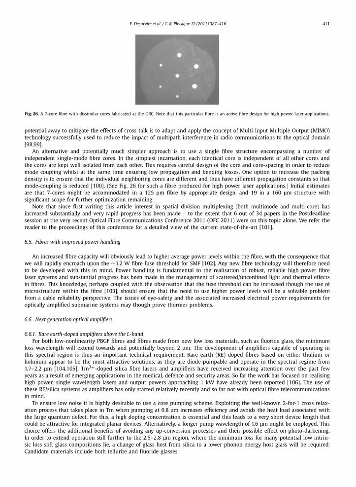
E. Desurvire et al. / C. R. Physique 12 (2011) 387–416 411
Fig. 26. A 7-core fibre with dissimilar cores fabricated at the ORC. Note that this particular fibre is an active fibre design for high power laser applications.
potential away to mitigate the effects of cross-talk is to adapt and apply the concept of Multi-Input Multiple Output (MIMO)technology successfully used to reduce the impact of multipath interference in radio communications to the optical domain[98,99].
An alternative and potentially much simpler approach is to use a single fibre structure encompassing a number ofindependent single-mode fibre cores. In the simplest incarnation, each identical core is independent of all other cores andthe cores are kept well isolated from each other. This requires careful design of the core and core-spacing in order to reducemode coupling whilst at the same time ensuring low propagation and bending losses. One option to increase the packingdensity is to ensure that the individual neighboring cores are different and thus have different propagation constants so thatmode-coupling is reduced [100]. (See Fig. 26 for such a fibre produced for high power laser applications.) Initial estimatesare that 7-cores might be accommodated in a 125 μm fibre by appropriate design, and 19 in a 160 μm structure withsignificant scope for further optimization remaining.
Note that since first writing this article interest in spatial division multiplexing (both multimode and multi-core) hasincreased substantially and very rapid progress has been made – to the extent that 6 out of 34 papers in the Postdeadlinesession at the very recent Optical Fibre Communications Conference 2011 (OFC 2011) were on this topic alone. We refer thereader to the proceedings of this conference for a detailed view of the current state-of-the-art [101].
6.5. Fibres with improved power handling
An increased fibre capacity will obviously lead to higher average power levels within the fibre, with the consequence thatwe will rapidly encroach upon the ∼1.2 W fibre fuse threshold for SMF [102]. Any new fibre technology will therefore needto be developed with this in mind. Power handling is fundamental to the realisation of robust, reliable high power fibrelaser systems and substantial progress has been made in the management of scattered/unconfined light and thermal effectsin fibres. This knowledge, perhaps coupled with the observation that the fuse threshold can be increased though the use ofmicrostructure within the fibre [103], should ensure that the need to use higher power levels will be a solvable problemfrom a cable reliability perspective. The issues of eye-safety and the associated increased electrical power requirements foroptically amplified submarine systems may though prove thornier problems.
6.6. Next generation optical amplifiers
6.6.1. Rare earth-doped amplifiers above the L-bandFor both low-nonlinearity PBGF fibres and fibres made from new low loss materials, such as fluoride glass, the minimum
loss wavelength will extend towards and potentially beyond 2 μm. The development of amplifiers capable of operating inthis spectral region is thus an important technical requirement. Rare earth (RE) doped fibres based on either thulium orholmium appear to be the most attractive solutions, as they are diode-pumpable and operate in the spectral regime from1.7–2.2 μm [104,105]. Tm3+-doped silica fibre lasers and amplifiers have received increasing attention over the past fewyears as a result of emerging applications in the medical, defence and security areas. So far the work has focused on realisinghigh power, single wavelength lasers and output powers approaching 1 kW have already been reported [106]. The use ofthese RE/silica systems as amplifiers has only started relatively recently and so far not with optical fibre telecommunicationsin mind.
To ensure low noise it is highly desirable to use a core pumping scheme. Exploiting the well-known 2-for-1 cross relax-ation process that takes place in Tm when pumping at 0.8 μm increases efficiency and avoids the heat load associated withthe large quantum defect. For this, a high doping concentration is essential and this leads to a very short device length thatcould be attractive for integrated planar devices. Alternatively, a longer pump wavelength of 1.6 μm might be employed. Thischoice offers the additional benefits of avoiding any up-conversion processes and their possible effect on photo-darkening.In order to extend operation still further to the 2.5–2.8 μm region, where the minimum loss for many potential low intrin-sic loss soft glass compositions lie, a change of glass host from silica to a lower phonon energy host glass will be required.Candidate materials include both tellurite and fluoride glasses.

412 E. Desurvire et al. / C. R. Physique 12 (2011) 387–416
6.6.2. Rare earth-doped amplifiers below the C-bandThe development of low water loss fibres such as OFS “All-Wave” means that fibre amplifiers are now needed for the
1.3–1.5 μm range, extending perhaps to even shorter wavelengths for distribution/datacomms applications. Candidate op-tions include Raman amplifiers [107], RE ions in low phonon energy materials such as ZBLAN and tellurite glasses [105],neodymium-doped fibres [105] and, most recently, bismuth-doped fibres [108]. Gain from bismuth-doping came as a sur-prise to the community and the underlying mechanisms by which the gain is obtained are still not well understood,highlighting the continued importance of fundamental material studies. Powerful emerging in-fibre distributed filteringtechnologies based on antiresonant effects such as those exploited in all-solid bandgap fibres [109] will also be helpful tosuppress unwanted transitions.
An alternative approach to RE-fibre amplification with its defined windows of operation is Raman scattering, which canprovide gain at any wavelength within the transparency window of the host glass [107]. Moreover, by shaping the pumpspectrum one can control the gain spectrum to ensure flat gain. While an established technology, application has beenrestricted primarily to distributed amplification in long haul systems to complement the use of the EDFA, rather than asa discrete amplifier. Traditionally, Raman amplifiers are pumped using arrays of semiconductor lasers, or by Raman lasersbased on complex cascaded resonators formed of nested gratings, or arrays of couplers. Whilst such amplifiers can givereasonable performance it is difficult to get truly broadband coverage in a compact device. Developments in fibre lasertechnology open up new pumping options. For example, the use of counter-propagating, rectangular-shaped optical pulsesof differing amplitudes to synthesise complex, broadband gain spectra for pumping lumped Raman amplifier configurations[110].
6.6.3. Amplifiers for spatial division multiplexed systemsWith significant interest growing in SDM the need for amplifiers compatible with SDM transmission fibres emerges.
From a cost and simplicity perspective such an amplifier would ideally amplify all spatial channels simultaneously (be theyindividual modes or separate cores). Given the noise and cross-talk requirements this represents a huge challenge and todate little (if any) progress has been reported. The option of demultiplexing the individual channels and the use of multipleconventional (single-mode) amplifiers (one per spatial channel) followed by a further multiplexing process always existsand perhaps provides a more realistic, albeit less attractive, approach – although, even here, many challenges exist at thecomponent level. Without a practical, cost-effective amplifier solution the use of SDM for long haul transmission is clearlylikely to be of very limited interest.
6.6.4. Phase sensitive parametric amplifiersAll-optical communication systems use optical amplifiers to compensate for fibre loss. Current systems based on con-
ventional binary modulation formats, e.g., NRZ or RZ, use either erbium-doped or Raman fibre amplifiers, both of whichproduce signal gain that is independent of the phase of the signal, and are thus classified as Phase Insensitive Amplifiers(PIAs). Such amplifiers are extremely robust and offer exceptional multi-wavelength system capabilities, but add quantumnoise to the signal that compromises performance. A second (parametric) form of amplification based on nonlinear opticsoffers Phase Sensitive Amplification (PSA). PSA can give low-noise operation (theoretically noise-free for certain implementa-tions) [111,112], phase-regeneration [113], and interesting photon correlation characteristics that are important to quantuminformation transmission and processing [114]. With the emergence of higher order Phase Shift Keying (PSK) signals thatrely upon phase coding, the question naturally emerges as to whether the use of PSA offers new opportunities in futureoptical networks. In recent works both ∼ 1 dB NF amplification [115], and high quality regeneration of binary PSK sig-nals at data rates as high as 40 GBit/s [116] have been demonstrated using an in-line “black box” implementation, whichrepresents a significant step forward in terms of practicality.
In Fig. 27 we show typical input and output constellation and eye diagrams measured on 10 Gbit/s DPSK data in theabsence (left) and presence (right) of a significant sinusoidal phase perturbation (±70 degrees sinusoidal modulation at5 GHz). The measurements illustrate the drastic phase noise reductions that can be achieved due to the periodic 2-levelphase response of the PSA.
The implications of a practical PSA technology within optical communications could potentially be profound, offeringbenefits such as: improved OSNRs – providing increased flexibility in terms of the constellation diagrams that might beused for M-PSK signals; reduced signal power requirements and associated nonlinear effects and; novel optical processingelements for M-PSK signals, including single and multichannel all-optical regenerators and monitoring devices.
6.7. Conclusions
In conclusion, we have described some of the major challenges facing network operators and designers trying to provisionfor the continued growth in internet traffic. It is clear that innovation in the underlying fibre infrastructure will be requiredsoon to avoid the looming capacity crunch that is likely to hit us within the next 10–15 years.
We have discussed a number of opportunities that if employed in isolation could provide around one order of magnitudeimprovement in transmission capacity for a single fibre and in combination perhaps up to two orders of magnitude improve-ment, enabling Petabit/s transmission. Clearly to realise this in practise will represent an enormous engineering challenge;however it is one that needs to be addressed in order to service societies increasing digital needs and expectations.

E. Desurvire et al. / C. R. Physique 12 (2011) 387–416 413
Fig. 27. Top – PSA implementation. Bottom – constellation and eye diagrams at PSA input (LHS) and output (RHS). Almost perfect signal quality is restoredwhen substantial phase noise is added to the input signal S [29].
7. Conclusion and perspectives
The field of optical communications traces back from the invention of the laser (1960) and relatively soon after, theoptical fibre (1966 to 1970); in turn, it is approaching its own “half-century maturity”. Since the original lab and industryvision, and beyond reasonable prediction, so much inventive technology has been accomplished indeed, in order to reach thecurrent state of art! While the same observation applies to radio cellular and satellite communications, optical technologiesmade the global network backbone, the high-speed Internet, a reality.
As we described it in Section 1, the originating optical communications breakthrough was the transition, from opticalfibres with 1 dB/m attenuation, to low-loss optical fibres, nowadays manufactured with 20 dB/100 km loss. Such transparent“lightpipes”, keep laser-light coherence and signal integrity over distances of one-hundred kilometres/miles. Over the sameearly period, semiconductor technology ensured the development of narrow-spectrum, microchip-scale, highly-reliable andefficient laser sources and photo-detectors. Altogether, optical communications technology would bring bandwidth.
The electronic bottleneck of early “repeaters”, which, in the early 1980s circumscribed the geographical horizon of opticaltelecoms, was alleviated through yet another sweeping revolution: in-line amplification by stimulated emission througherbium-doped fibres, the EDFA. Several wavelength channels could then be periodically repowered “at once”, without mutualinterference. Hence the golden age of WDM, which, in its early stage, one may rightly call the era of “virtually unlimitedbandwidth”. Alternatively, it could be called as well the era of “conquest for bandwidth”, because highly sophisticated meansto appropriate such a potential had to be invented and deployed. Thus, the world currently enjoys “global bandwidth”, whichis as much a hardware as a software concept, the first being generally overlooked from any end-user standpoint.
Then, what about the remaining challenges lying ahead in our “modern telecommunications”?Next, we have seen (Section 2) that discrete transmit/receive components, mostly InP-based, are at the root of the optical
communication industry. Yet, improving their characteristics towards higher performance in speed, chip size, electro-opticalconversion efficiency and high temperature operation remains a major challenge for the coming decade. This technologywill have to meet a growing transmission capacity demand, while offering the increased requested wavelength agility and,simultaneously, a low environmental cost, i.e. low energy/material consumptions. As for the societal impact, next to globalconnectivity, there are emerging markets such as security, medical imaging, pollution sensing, to quote a few.
Section 3 has also highlighted the fact and reality that after 50 years, the utility of the laser continues to thrive andprosper. In this respect, large-scale Photonic Integrated Circuits utilising arrays of semiconductor lasers and photo-receivers,are no exception. More and more technology integration is key to massive or global deployment, at ever-reduced costs andenergy savings.
But it is not all about components technology. Key concepts of high-bit-rate transmission had to be revisited, stretchingsystem design to ultimate performance, exploring the boundaries of Physics and fundamental Laws. At the same time, thenew solutions for “more transmission bandwidth” had to respect the basic engineering rules of simplicity, cost-effectiveness,and short time-to-market. Section 4 illustrated this through the revival of coherent detection. Along with digital signal pro-cessing, including powerful and efficient codes for error correction, and the introduction of multi-level modulation formats,a strong momentum has been gathered in high-speed, long-haul fibre links. Research is now all about breaking the current,status of 112 Petabit/s km performance.
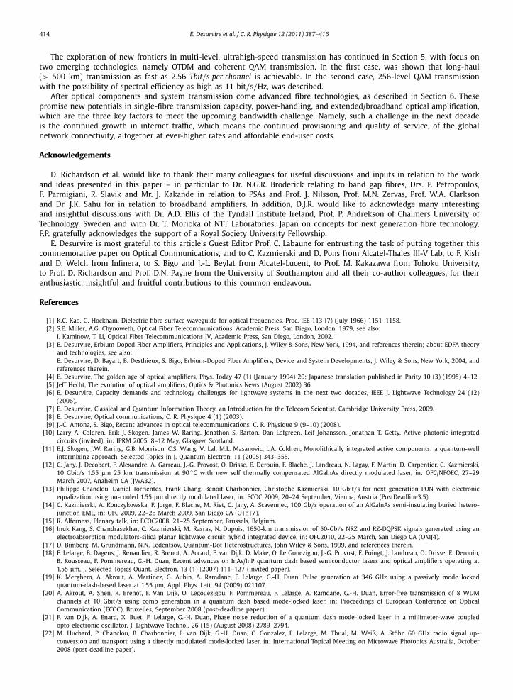
414 E. Desurvire et al. / C. R. Physique 12 (2011) 387–416
The exploration of new frontiers in multi-level, ultrahigh-speed transmission has continued in Section 5, with focus ontwo emerging technologies, namely OTDM and coherent QAM transmission. In the first case, was shown that long-haul(> 500 km) transmission as fast as 2.56 Tbit/s per channel is achievable. In the second case, 256-level QAM transmissionwith the possibility of spectral efficiency as high as 11 bit/s/Hz, was described.
After optical components and system transmission come advanced fibre technologies, as described in Section 6. Thesepromise new potentials in single-fibre transmission capacity, power-handling, and extended/broadband optical amplification,which are the three key factors to meet the upcoming bandwidth challenge. Namely, such a challenge in the next decadeis the continued growth in internet traffic, which means the continued provisioning and quality of service, of the globalnetwork connectivity, altogether at ever-higher rates and affordable end-user costs.
Acknowledgements
D. Richardson et al. would like to thank their many colleagues for useful discussions and inputs in relation to the workand ideas presented in this paper – in particular to Dr. N.G.R. Broderick relating to band gap fibres, Drs. P. Petropoulos,F. Parmigiani, R. Slavik and Mr. J. Kakande in relation to PSAs and Prof. J. Nilsson, Prof. M.N. Zervas, Prof. W.A. Clarksonand Dr. J.K. Sahu for in relation to broadband amplifiers. In addition, D.J.R. would like to acknowledge many interestingand insightful discussions with Dr. A.D. Ellis of the Tyndall Institute Ireland, Prof. P. Andrekson of Chalmers University ofTechnology, Sweden and with Dr. T. Morioka of NTT Laboratories, Japan on concepts for next generation fibre technology.F.P. gratefully acknowledges the support of a Royal Society University Fellowship.
E. Desurvire is most grateful to this article’s Guest Editor Prof. C. Labaune for entrusting the task of putting together thiscommemorative paper on Optical Communications, and to C. Kazmierski and D. Pons from Alcatel-Thales III-V Lab, to F. Kishand D. Welch from Infinera, to S. Bigo and J.-L. Beylat from Alcatel-Lucent, to Prof. M. Kakazawa from Tohoku University,to Prof. D. Richardson and Prof. D.N. Payne from the University of Southampton and all their co-author colleagues, for theirenthusiastic, insightful and fruitful contributions to this common endeavour.
References
[1] K.C. Kao, G. Hockham, Dielectric fibre surface waveguide for optical frequencies, Proc. IEE 113 (7) (July 1966) 1151–1158.[2] S.E. Miller, A.G. Chynoweth, Optical Fiber Telecommunications, Academic Press, San Diego, London, 1979, see also:
I. Kaminow, T. Li, Optical Fiber Telecommunications IV, Academic Press, San Diego, London, 2002.[3] E. Desurvire, Erbium-Doped Fiber Amplifiers, Principles and Applications, J. Wiley & Sons, New York, 1994, and references therein; about EDFA theory
and technologies, see also:E. Desurvire, D. Bayart, B. Desthieux, S. Bigo, Erbium-Doped Fiber Amplifiers, Device and System Developments, J. Wiley & Sons, New York, 2004, andreferences therein.
[4] E. Desurvire, The golden age of optical amplifiers, Phys. Today 47 (1) (January 1994) 20; Japanese translation published in Parity 10 (3) (1995) 4–12.[5] Jeff Hecht, The evolution of optical amplifiers, Optics & Photonics News (August 2002) 36.[6] E. Desurvire, Capacity demands and technology challenges for lightwave systems in the next two decades, IEEE J. Lightwave Technology 24 (12)
(2006).[7] E. Desurvire, Classical and Quantum Information Theory, an Introduction for the Telecom Scientist, Cambridge University Press, 2009.[8] E. Desurvire, Optical communications, C. R. Physique 4 (1) (2003).[9] J.-C. Antona, S. Bigo, Recent advances in optical telecommunications, C. R. Physique 9 (9–10) (2008).
[10] Larry A. Coldren, Erik J. Skogen, James W. Raring, Jonathon S. Barton, Dan Lofgreen, Leif Johansson, Jonathan T. Getty, Active photonic integratedcircuits (invited), in: IPRM 2005, 8–12 May, Glasgow, Scotland.
[11] E.J. Skogen, J.W. Raring, G.B. Morrison, C.S. Wang, V. Lal, M.L. Masanovic, L.A. Coldren, Monolithically integrated active components: a quantum-wellintermixing approach, Selected Topics in J. Quantum Electron. 11 (2005) 343–355.
[12] C. Jany, J. Decobert, F. Alexandre, A. Garreau, J.-G. Provost, O. Drisse, E. Derouin, F. Blache, J. Landreau, N. Lagay, F. Martin, D. Carpentier, C. Kazmierski,10 Gbit/s 1.55 μm 25 km transmission at 90 ◦C with new self thermally compensated AlGaInAs directly modulated laser, in: OFC/NFOEC, 27–29March 2007, Anaheim CA (JWA32).
[13] Philippe Chanclou, Daniel Torrientes, Frank Chang, Benoit Charbonnier, Christophe Kazmierski, 10 Gbit/s for next generation PON with electronicequalization using un-cooled 1.55 μm directly modulated laser, in: ECOC 2009, 20–24 September, Vienna, Austria (PostDeadline3.5).
[14] C. Kazmierski, A. Konczykowska, F. Jorge, F. Blache, M. Riet, C. Jany, A. Scavennec, 100 Gb/s operation of an AlGaInAs semi-insulating buried hetero-junction EML, in: OFC 2009, 22–26 March 2009, San Diego CA (OThT7).
[15] R. Alferness, Plenary talk, in: ECOC2008, 21–25 September, Brussels, Belgium.[16] Inuk Kang, S. Chandrasekhar, C. Kazmierski, M. Rasras, N. Dupuis, 1650-km transmission of 50-Gb/s NRZ and RZ-DQPSK signals generated using an
electroabsorption modulators-silica planar lightwave circuit hybrid integrated device, in: OFC2010, 22–25 March, San Diego CA (OMJ4).[17] D. Bimberg, M. Grundmann, N.N. Ledentsov, Quantum-Dot Heterostructures, John Wiley & Sons, 1999, and references therein.[18] F. Lelarge, B. Dagens, J. Renaudier, R. Brenot, A. Accard, F. van Dijk, D. Make, O. Le Gouezigou, J.-G. Provost, F. Poingt, J. Landreau, O. Drisse, E. Derouin,
B. Rousseau, F. Pommereau, G.-H. Duan, Recent advances on InAs/InP quantum dash based semiconductor lasers and optical amplifiers operating at1.55 μm, J. Selected Topics Quant. Electron. 13 (1) (2007) 111–127 (invited paper).
[19] K. Merghem, A. Akrout, A. Martinez, G. Aubin, A. Ramdane, F. Lelarge, G.-H. Duan, Pulse generation at 346 GHz using a passively mode lockedquantum-dash-based laser at 1.55 μm, Appl. Phys. Lett. 94 (2009) 021107.
[20] A. Akrout, A. Shen, R. Brenot, F. Van Dijk, O. Legouezigou, F. Pommereau, F. Lelarge, A. Ramdane, G.-H. Duan, Error-free transmission of 8 WDMchannels at 10 Gbit/s using comb generation in a quantum dash based mode-locked laser, in: Proceedings of European Conference on OpticalCommunication (ECOC), Bruxelles, September 2008 (post-deadline paper).
[21] F. van Dijk, A. Enard, X. Buet, F. Lelarge, G.-H. Duan, Phase noise reduction of a quantum dash mode-locked laser in a millimeter-wave coupledopto-electronic oscillator, J. Lightwave Technol. 26 (15) (August 2008) 2789–2794.
[22] M. Huchard, P. Chanclou, B. Charbonnier, F. van Dijk, G.-H. Duan, C. Gonzalez, F. Lelarge, M. Thual, M. Weiß, A. Stöhr, 60 GHz radio signal up-conversion and transport using a directly modulated mode-locked laser, in: International Topical Meeting on Microwave Photonics Australia, October2008 (post-deadline paper).
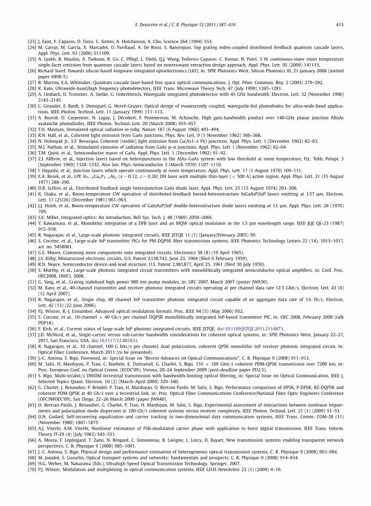
E. Desurvire et al. / C. R. Physique 12 (2011) 387–416 415
[23] J. Faist, F. Capasso, D. Sivco, C. Sirtori, A. Hutchinson, A. Cho, Science 264 (1994) 553.[24] M. Carras, M. Garcia, X. Marcadet, O. Parillaud, A. De Rossi, S. Bansropun, Top grating index-coupled distributed feedback quantum cascade lasers,
Appl. Phys. Lett. 93 (2008) 011109.[25] A. Lyakh, R. Maulini, A. Tsekoun, R. Go, C. Pflügl, L. Diehl, Q.J. Wang, Federico Capasso, C. Kumar, N. Patel, 3 W continuous-wave room temperature
single-facet emission from quantum cascade lasers based on nonresonant extraction design approach, Appl. Phys. Lett. 95 (2009) 141113.[26] Richard Soref, Towards silicon-based longwave integrated optoelectronics (LIO), in: SPIE Photonics West, Silicon Photonics III, 21 January 2008 (invited
paper 6898-5).[27] R. Martini, E.A. Whittaker, Quantum cascade laser-based free space optical communications, J. Opt. Fiber. Commun. Rep. 2 (2005) 279–292.[28] K. Kato, Ultrawide-band/high frequency photodetectors, IEEE Trans. Microwave Theory Tech. 47 (July 1999) 1265–1281.[29] A. Umbach, D. Trommer, A. Sietke, G. Unterbörsch, Waveguide integrated photodetector with 45 GHz bandwidth, Electron. Lett. 32 (November 1996)
2143–2145.[30] L. Giraudet, F. Banfi, S. Demiguel, G. Hervé-Gruyer, Optical design of evanescently coupled, waveguide-fed photodiodes for ultra-wide-band applica-
tions, IEEE Photon. Technol. Lett. 11 (January 1999) 111–113.[31] A. Rouvié, D. Carpentier, N. Lagay, J. Décobert, F. Pommereau, M. Achouche, High gain-bandwidth product over 140-GHz planar junction AlInAs
avalanche photodiodes, IEEE Photon. Technol. Lett. 20 (March 2008) 455–457.[32] T.H. Maiman, Stimulated optical radiation in ruby, Nature 187 (6 August 1960) 493–494.[33] R.N. Hall, et al., Coherent light emission from GaAs junctions, Phys. Rev. Lett. 9 (1 November 1962) 366–368.[34] N. Holonyak Jr., S.F. Bevacqua, Coherent (visible) light emission from Ga(As1–x Px) junctions, Appl. Phys. Lett. 1 (December 1962) 82–83.[35] M.I. Nathan, et al., Stimulated emission of radiation from GaAs p–n junctions, Appl. Phys. Lett. I (November 1962) 62–64.[36] T.M. Quist, et al., Semiconductor maser of GaAs, Appl. Phys. Lett. 1 (December 1962) 91–92.[37] Z.I. Alfërov, et al., Injection lasers based on heterojunctions in the AlAs–GaAs system with low threshold at room temperature, Fiz: Tekh. Polupr. 3
(September 1969) 1328–1332. Also Sov. Phys.-Semiconductor 3 (March 1970) 1107–1110.[38] I. Hayashi, et al., Junction lasers which operate continuously at room temperature, Appl. Phys. Lett. 17 (1 August 1970) 109–111.[39] E.A. Rezek, et al., LPE In1−xGaxP1−zAsz (x ∼ 0.12, z ∼ 0.26) DH laser with multiple thin-layer (< 500 A) active region, Appl. Phys. Lett. 31 (15 August
1977) 288–290.[40] D.R. Scifres, et al., Distributed feedback single heterojunction GaAs diode laser, Appl. Phys. Lett. 25 (15 August 1974) 203–206.[41] K. Utaka, et al., Room-temperature CW operation of distributed-feedback buried-heterostructure InGaAsP/InP lasers emitting at 1.57 μm, Electron.
Lett. 17 (25/26) (December 1981) 961–963.[42] J.J. Hsieh, et al., Room-temperature CW operation of GaInAsP/InP double-heterostructure diode lasers emitting at 1.1 μm, Appl. Phys. Lett. 28 (1976)
709.[43] S.E. Miller, Integrated optics: An introduction, Bell Sys. Tech. J. 48 (1969) 2059–2069.[44] Y. Kawamura, et al., Monolithic integration of a DFB laser and an MQW optical modulator in the 1.5 μm wavelength range, IEEE JQE QE-23 (1987)
915–918.[45] R. Nagarajan, et al., Large-scale photonic integrated circuits, IEEE JSTQE 11 (1) (January/February 2005) 50.[46] S. Corzine, et al., Large-scale InP transmitter PICs for PM-DQPSK fiber transmission systems, IEEE Photonics Technology Letters 22 (14), 1015–1017,
art. no. 5458061.[47] G.E. Moore, Cramming more components onto integrated circuits, Electronics 38 (8) (19 April 1965).[48] J.S. Kilby, Miniaturized electronic circuits, U.S. Patent 3,138,743, June 23, 1964 (filed 6 February 1959).[49] R.N. Noyce, Semiconductor device-and-lead structure, U.S. Patent 2,981,877, April 25, 1961 (filed 30 July 1959).[50] S. Murthy, et al., Large-scale photonic integrated circuit transmitters with monolithically integrated semiconductor optical amplifiers, in: Conf. Proc.
OFC2008, OWE1, 2008.[51] G. Yang, et al., Grating stabilised high power 980 nm pump modules, in: OFC 2007, March 2007 (poster JWA30).[52] M. Kato, et al., 40-channel transmitter and receiver photonic integrated circuits operating at per channel data rate 12.5 Gbit/s, Electron. Lett. 43 (8)
(12 April 2007).[53] R. Nagarajan, et al., Single chip, 40 channel InP transmitter photonic integrated circuit capable of an aggregate data rate of 1.6 Tb/s, Electron.
Lett. 42 (13) (22 June 2006).[54] P.J. Winzer, R.-J. Essiambre, Advanced optical modulation formats, Proc. IEEE 94 (5) (May 2006) 952.[55] S. Corzine, et al., 10-channel × 40 Gb/s per channel DQPSK monolithically integrated InP-based transmitter PIC, in: OFC 2008, February 2008 (talk
PDP18).[56] F. Kish, et al., Current status of large-scale InP photonic integrated circuits, IEEE JSTQE, doi:10.1109/JSTQE.2011.2114873.[57] J.D. McNicol, et al., Single-carrier versus sub-carrier bandwidth considerations for coherent optical systems, in: SPIE Photonics West, January 22–27,
2011, San Francisco, USA, doi:10.1117/12.881631.[58] R. Nagarajan, et al., 10 channel, 100 G bits/s per channel, dual polarization, coherent QPSK monolithic InP receiver photonic integrated circuit, in:
Optical Fiber Conference, March 2011 (to be presented).[59] J.-C. Antona, S. Bigo, Foreword, in: Special Issue on “Recent Advances on Optical Communications”, C. R. Physique 9 (2008) 911–913.[60] M. Salsi, H. Mardoyan, P. Tran, C. Koebele, E. Dutisseuil, G. Charlet, S. Bigo, 155 × 100 Gbit/s coherent PDM-QPSK transmission over 7200 km, in:
Proc. European Conf. on Optical Comm. (ECOC’09), Vienna, 20–24 September 2009 (post-deadline paper PD2.5).[61] S. Bigo, Multi-terabit/s DWDM terrestrial transmission with bandwidth-limiting optical filtering, in: Special Issue on Optical Communication, IEEE J.
Selected Topics Quant. Electron. 10 (2) (March–April 2004) 329–340.[62] G. Charlet, J. Renaudier, P. Brindel, P. Tran, H. Mardoyan, O. Bertran Pardo, M. Salsi, S. Bigo, Performance comparison of DPSK, P-DPSK, RZ-DQPSK and
coherent PDM-QPSK at 40 Gb/s over a terrestrial link, in: Proc. Optical Fiber Communications Conference/National Fiber Optic Engineers Conference(OFC/NFOEC’09), San Diego, 22–26 March 2009 (paper JWA40).
[63] O. Bertran-Pardo, J. Renaudier, G. Charlet, P. Tran, H. Mardoyan, M. Salsi, S. Bigo, Experimental assessment of interactions between nonlinear impair-ments and polarization mode dispersion in 100-Gb/s coherent systems versus receiver complexity, IEEE Photon. Technol. Lett. 21 (1) (2009) 51–53.
[64] D.N. Godard, Self-recovering equalization and carrier tracking in two-dimensional data communication systems, IEEE Trans. Comm. COM-28 (11)(November 1980) 1867–1875.
[65] A.J. Viterbi, A.M. Viterbi, Nonlinear estimation of PSK-modulated carrier phase with application to burst digital transmission, IEEE Trans. Inform.Theory IT-29 (4) (July 1983) 543–551.
[66] A. Morea, F. Leplingard, T. Zami, N. Brogard, C. Simonneau, B. Lavigne, L. Lorcy, D. Bayart, New transmission systems enabling transparent networkperspectives, C. R. Physique 9 (2008) 985–1001.
[67] J.-C. Antona, S. Bigo, Physical design and performance estimation of heterogeneous optical transmission systems, C. R. Physique 9 (2008) 963–984.[68] M. Joindot, S. Gosselin, Optical transport systems and networks: fundamentals and prospects, C. R. Physique 9 (2008) 914–934.[69] H.G. Weber, M. Nakazawa (Eds.), Ultrahigh-Speed Optical Transmission Technology, Springer, 2007.[70] P.J. Winzer, Modulation and multiplexing in optical communication systems, IEEE LEOS Newsletter 23 (1) (2009) 4–10.

416 E. Desurvire et al. / C. R. Physique 12 (2011) 387–416
[71] A.D. Ellis, Modulation formats which approach the Shannon limit, in: OFC2009 (OMM4).[72] M. Nakazawa, M. Yoshida, K. Kasai, J. Hongou, 20 Msymbol/s, 64 and 128 QAM coherent optical transmission over 525 km using heterodyne detection
with frequency-stabilised laser, Electron. Lett. 43 (2006) 710–712.[73] M. Nakazawa, T. Yamamoto, K.R. Tamura, 1.28 Tbit/s-70 km OTDM transmission using third- and fourth-order simultaneous dispersion compensation
with a phase modulator, Electron. Lett. 36 (24) (2000) 2027–2029.[74] H.G. Weber, S. Ferber, M. Kroh, C. Schmidt-Langhorst, R. Ludwig, V. Marembert, C. Boerner, F. Futami, S. Watanabe, C. Schubert, Single channel
1.28 Tbit/s and 2.56 Tbit/s DQPSK transmission, Electron. Lett. 42 (3) (2006) 178–179.[75] M. Nakazawa, T. Hirooka, F. Futami, S. Watanabe, Ideal distortion-free transmission using optical Fourier transformation and Fourier transform-limited
optical pulses, IEEE Photon. Technol. Lett. 16 (4) (2004) 1059–1061.[76] T. Hirano, P. Guan, T. Hirooka, M. Nakazawa, 640 Gbit/s single-polarization DPSK transmission over 525 km with time-domain optical Fourier trans-
formation in a round-trip configuration, in: OFC 2010 (OThD7).[77] K. Tajima, All-optical switch with switch-off time unrestricted by carrier lifetime, Jpn. J. Appl. Phys. 32 (1993) L1746–L1749.[78] C. Boerner, V. Marembert, S. Ferber, C. Schubert, C. Schmidt-Langhorst, R. Ludwig, H.G. Weber, 320 Gbit/s clock recovery with electro-optical PLL
using a bidirectionally operated electroabsorption modulator as phase comparator, in: OFC 2005 (OTuO3).[79] C.E. Shannon, A mathematical theory of communication, Bell Syst. Tech. J. 27 (1948) 379–423, and 623-656.[80] A.H. Gnauck, P.J. Winzer, C.R. Doerr, L.L. Buhl, 10 × 112-Gb/s PDM 16-QAM transmission over 630 km of fiber with 6.2-b/s/Hz spectral efficiency,
in: OFC2009 (PDPB8).[81] H. Takahashi, A. Al Amin, S.L. Jansen, I. Morita, H. Tanaka, DWDM transmission with 7.0-bit/s/Hz spectral efficiency using 8 × 65.1-Gbit/s coherent
PDM-OFDM signals, in: OFC 2009 (PDPB7).[82] M. Nakazawa, S. Okamoto, T. Omiya, K. Kasai, M. Yoshida, 256-QAM (64 Gb/s) coherent optical transmission over 160 km with an optical bandwidth
of 5.4 GHz, IEEE Photon. Technol. Lett. 22 (3) (2010) 185–187.[83] K. Kasai, A. Suzuki, M. Yoshida, M. Nakazawa, Performance improvement of an acetylene (C2H2) frequency-stabilised fiber laser, IEICE Electron.
Express 3 (2006) 487–492.[84] H. Nyquist, Certain topics in telegraph transmission theory, AIEE Trans. 47 (1928) 617–644.[85] J.G. Proakis, Digital Communications, 4th edition, McGraw Hill, 2000.[86] See e.g. http://www.ciscosecure.net/en/US/solutions/collateral/ns341/ns525/ns537/ns827/White_paper_c11-481360_ns827_Networking_Solutions_
White_Paper.html.[87] P.P. Mitra, J.B. Stark, Nonlinear limits to the information capacity of optical fibre communications, Nature 411 (2001) 1027–1030.[88] A.D. Ellis, J. Zhao, D. Cotter, Approaching the non-linear Shannon limit, J. Lightwave Technol. 28 (4) (2010) 423–433.[89] K. Nagayama, et al., Ultra-low-loss (0.1484 dB/km) pure silica core fiber and extension of transmission distance, Electron. Lett. 38 (2002) 1168–1169.[90] J. Schroeder, R. Mohr, P.B. Macedo, C.J. Montrose, Rayleigh and Brillouin scattering in K2O–SiO2 glasses, J. Am. Ceram. Soc. 56 (1973) 510–514.[91] K. Tajima, et al., Low Rayleigh scattering P2O5–F–SiO2 glasses, IEEE J. Lightwave Technol. 10 (1992) 1532–1534.[92] S.R. Nagel, Fiber materials and fabrication methods, in: Stewart E. Miller, Ivan P. Kaminow (Eds.), Optical Fiber Communications II, Academic Press,
1988.[93] S.F. Carter, et al., Low loss fluoride fiber by reduced pressure casting, Electron. Lett. 26 (2005) 2115–2116.[94] R.F. Cregan, B.J. Mangan, J.C. Knight, T.A. Birks, P.St.J. Russell, P.J. Roberts, D.C. Allan, Single-mode photonic band gap guidance of light in air, Sci-
ence 285 (1999) 1537–1539.[95] P.J. Roberts, F. Couny, H. Sabert, B.J. Mangan, D.P. Williams, L. Farr, M.W. Mason, A. Tomlinson, T.A. Birks, J.C. Knight, P.S.J. Russell, Ultimate low loss
of hollow-core photonic crystal fibers, Opt. Express 13 (2005) 236–244.[96] J.K. Lyngso, et al., Realization of 7-cell hollow core photonic crystal fibers with low-loss in the region between 1.4 μm and 2.3 μm, in: Proc. OECC’09
(paper FS1).[97] C.J. Hensley, et al., Silica-glass contribution to the effective nonlinearity of hollow-core photonic bandgap fibers, Opt. Express 15 (2007) 3507–3512.[98] H. Stuart, Dispersive multiplexing in multimode optical fiber, Science 289 (2000) 281–283.[99] A. Tarighat, R.C.J. Hsu, A. Shah, A.H. Sayed, B. Jalali, Fundamentals and challenges of optical multiple-input multiple-output multimode fiber links,
IEEE Communications Magazine 45 (2007) 57–63.[100] M. Koshiba, K. Saitoh, Y. Kokubun, Heterogeneous multicore fibers: proposal and design principle, IEICE Electronics Express 6 (2009) 98–103.[101] See postdeadline paper volume, in: Proc. Optical Fiber Communications Conference/National Fiber Optic Engineers Conference (OFC/NFOEC’11), Los
Angeles, 6–10 March 2011.[102] D.P. Hand, P.St.J. Russell, Solitary thermal shock-waves and optical damage in optical fibers: The fiber fuse, Opt. Lett. 13 (1988) 767–769.[103] N. Hanzawa, K. Kurokawa, K. Tsujikawa, T. Matsui, S. Tomita, Suppression of fiber fuse propagation in photonic crystal fiber (PCF) and hole assisted
fiber, in: Technical Digest of Microoptics Conference, 2009, p. M7.[104] D.C. Hanna, R.M. Percival, I.R. Perry, R.G. Smart, P.J. Suni, J.E. Townsend, A.C. Tropper, Continuous-wave oscillation of a monomode thulium-doped
fiber laser, Electron. Lett. 24 (19) (1998) 1222–1223.[105] M. Digonnet, Rare Earth Doped Fiber Lasers and Amplifiers, Marcel Dekker Inc., 1993.[106] P.F. Moulton, G.A. Rines, E.V. Slobodtchikov, et al., Tm-doped fiber lasers: Fundamentals and power scaling, IEEE J. Selected Topics Quant. Electron. 15
(2009) 85–92.[107] M.N. Islam, Raman amplifiers for telecommunications, IEEE J. Selected Topics Quant. Electron. 8 (2002) 548–558.[108] E.M. Dianov, et al., High-power cw bismuth-fiber lasers, J. Opt. Soc. Amer. B – Opt. Phys. 24 (2007) 1749.[109] A. Shirakawa, H. Maruyama, K. Ueda, et al., High-power Yb-doped photonic bandgap fiber amplifier at 1150–1200 nm, Optics Express 17 (2009)
447–454.[110] C. Farrell, C. Codemard, J. Nilsson, A Raman fiber amplifier generating simultaneous gain across multiple Stokes orders by using step shaped optical
pulses, in: Europhoton 2008, Paris, France (paper XX).[111] H. Haus, J.A. Mullen, Phys. Rev. 128 (1962) 2407.[112] C.M. Caves, Quantum limits in noise in linear amplifiers, Phys. Rev. D 26 (1982) 1817–1839.[113] K. Croussore, G. Li, Amplitude regeneration of RZ-DPSK signals based on four-wave mixing in fiber, Electron. Lett. 43 (2007) 177–178.[114] C.J. McKinstrie, M.G. Raymer, S. Radic, M.V. Vasilyev, Quantum mechanics of phase sensitive amplification in a fiber, Opt. Commun. 257 (2006)
146–163.[115] Z. Tong, C. Lundström, A. Bogris, M. Karlsson, P. Andrekson, D. Syvridis, Measurement of sub-1 dB noise figure in a non-degenerate cascaded phase
sensitive fibre parametric amplifier, in: Proceedings of ECOC 2009 (Mo. 1.1.2).[116] R. Slavik, F. Parmigiani, J. Kakande, C. Lundström, M. Sjödin, P. Andrekson, R. Weerasuriya, S. Sygletos, A.D. Ellis, L. Grüner-Nielsen, D. Jakobsen, S.
Herstrøm, R. Phelan, J. O’Gorman, A. Bogris, D. Syvridis, S. Dasgupta, P. Petropoulos, D.J. Richardson, All-optical phase and amplitude regenerator fornext-generation telecommunications systems, Nature Photonics 4 (2010) 690–695.


![Leukocytes express activation lipopolysaccharide appear ... · free)/1% goat serum] for 30 min at roomtemperature. Then theywereincubatedwithanti-Cx43 antibody(1:100inblocking solution)](https://img.dokumen.tips/doc/110x75/603f27b1951d67438b291286/leukocytes-express-activation-lipopolysaccharide-appear-free1-goat-serum.jpg)


