Embed Size (px)
Citation preview

PDFlib PLOP: PDF Linearization, Optimization, Protection
Page inserted by evaluation versionwww.pdflib.com – [email protected]

277
Scanning Tunneling Microscopy (STM) on Physisorbed Chemical Groups of Individual Immobilized Molecules
YISHAY MANASSENa AND DOV SHACHAL
Department of Chemical Physics, Weizmann Institute of Science Rehovot 76100, Israel
ABSTRACT: Most scanning tunneling microscopy (STM) studies of adsorbed moleculesare performed either on molecules that are chemically bound to the surface or are part of amolecular monolayer. In the first case, the chemical reaction with the surface changes thesurface local density of states. In the second one, the electrons tunnel through a physisorbedmolecule. In the study described in this paper STM imaging is performed on isolated mole-cules immobilized on a clean semiconductor surface where atomic resolution is observed.This is an intermediate case.
The adsorption behavior of diene molecules on Si(111)7 × 7 was investigated. The mol-ecules adsorb by reaction of the double bonds on the surface. In the reaction, the C=C bondis opened to create two neighboring Si−C bonds. Two such C=C bonds are used to immo-bilize the chain to the surface. The adsorption chemistry is affected not only by the natureof the Si−C bond but also by steric limitations.
Performing STM imaging on such systems ensures that the position of the immobilizedchemical group (in this case an aliphatic chain) could be clearly identified and that it waspossible to image parts of the molecule that are not chemically bound to the surface. STMimages of 1,13-tetradecadiene revealed a white protrusion in the location of the aliphaticchain. The increase in transmission is explained by an additional channel for tunneling:through bond tunneling. Long-range electron transfer through molecules is a widely knownchemical and biochemical process. This observation opens the possibility to investigate thisfundamental phenomenon in large details. The potential applications for molecular electron-ics are discussed.
Since its invention, the capability of the STM (scanning tunneling microscope) toimage individual molecules on the surface fascinated many chemists. Although sig-nificant progress was made in the direction of molecular imaging, still, the vast po-tential of the STM in solving questions of interest for the scientific communityinterested in chemistry remained largely unexploited. One problem is that despite re-cent impressive successes, STM images of adsorbed molecules did not achieve theresolution and the contrast of STM images on clean conducting surfaces (in partic-ular semiconductors). It is widely accepted that although the STM contrast can beexplained using molecular orbitals analysis, the exact mechanism in which the tun-neling electrons are transferred through the molecules is not completely understood.
The first STM experiments on molecular imaging were on relatively small mol-ecules which were chemisorbed on the surface. The contrast achieved in these sys-tems was due to changing the surface LDOS (local density of states). This includes
aPresent address: Department of Physics, Ben Gurion University of the Negev, P. 0. Box,653, Beer Sheva, 84105, Israel.

278 ANNALS NEW YORK ACADEMY OF SCIENCES
studies of NH3 adsorbed on Si(111)7 × 7,1 O2 on Si(111)7 × 7,2,3 O2 on GaAs4 andC2H4 on Pt(111).5 In these experiments it was normally difficult to see any molecu-lar feature and only the affected LDOS is distinguishable. When larger moleculeswere adsorbed on the surface, the molecular features were, many times, distinguish-able. In such systems, due to the strong chemical bond between the molecules andthe surface, and the large size of the molecule, the LDOS includes a relatively largecontribution from the molecular orbitals, and the STM image also reflects molecularfeatures. Such studies were performed for example on adsorbed naphthalene,6 azu-lene derivatives7 copper phthalocyanine,8 and benzene [coadsorbed with CO onRh(111)].9
However, most STM molecular imaging studies were performed on two dimen-sional molecular monolayers (Delamarche and Michel,10 Walba and colleagues,11
and Patrick and colleagues12 are only few examples). The hindered diffusion of eachmolecule as a result of the interaction with its neighbors in the monolayer causes im-mobilization of the molecule even if it is not chemically bonded to the surface. Arecent elegant demonstration to the importance of this immobilization in observinggood contrast was the study on adsorbed benzene (in a submonolayer coverage) neara step.13 In this study, it was possible to observe good contrast of the adsorbed mol-ecules only near a step, where the molecular diffusion is hindered by the step. As thedistance from the step increased, the resolution of the molecular image deteriorated.
In the attempt to develop new STM chemical applications, there have been manystudies on adsorbed monolayers that tried to demonstrate the capability of the STMto distinguish between different functional groups in physisorbed molecules. It wasshown that the STM is quite effective in resolving alkyl chains on the surface andthat the aromatic ring appears much brighter than the aliphatic chain.14,15 In contrastSTM studies on substituted alkanes on graphite indicated that the OH, COOH, andCl functional groups can not be distinguished from the methylene group,16–18 but theS atoms were easily resolved in STM images of thiols and disulfide compounds.Amide and anilide groups were also easily distinguishable. 18–20
The question of the precise mechanism of the STM operation on physisorbedmolecules is still not resolved. The molecules are normally imaged at bias voltagesfar from the HOMO (highest occupied molecular orbital) and the LUMO (lowest un-occupied molecular orbital) so tunneling through these orbitals (resonant tunneling)is excluded. One suggestion was that the LDOS is affected by the presence of themolecules, and that interaction of the HOMO and the LUMO with the surface is suf-ficient to perturb the surface LDOS.14,15 This is supported by the agreement betweenthe observed images and the HOMO and LUMO also in physisorbed molecules thatform a monolayer such as alkyl cyanobiphenyls (on graphite).15 Another suggestionwas that the molecule changes the surface local work function and that a moleculewith larger polarizability has a greater affect on the work function.21 However nei-ther of these mechanisms can explain the high transmission probability found formonolayers made of relatively long molecules or other systems where the tip sampleseparation is larger than 1 nm.22,23 In order to explain these observations, two chan-nels for tunneling were proposed, through space and through bond tunneling.24 Inthe through space channel, the electrons tunnel from the tip to the sample withoutinteraction with the molecule. In the through bond channel, the molecular orbitalcouples the tip and the surface. All orbitals whose tail reaches the Fermi level can

279MANASSEN & SHACHAL: SCANNING TUNNELING MICROSCOPY
contribute to this coupling (nonresonant tunneling). This is similar to the contrastmechanism observed in Xe atoms on Ni(110):25 Although the Xe atomic level is farabove the Fermi level, still the tail of this level at the Fermi level is enough to in-crease the tunneling probability and to create the STM contrast. This is connected tothe more general problem of understanding long distance electron transfer. It isknown for a long time26–29 that such electron transfer processes must be mediatedby the covalent bonds and the noncovalent interactions between the donor (of theelectron) and the acceptor. Taking into account the role of these mediations gives atunneling matrix element which is indeed exponential, but decays much slower withdistance, enabling electron transfer over distances of several nanometers. Long-range electron transfer is a fundamental part of many basic biochemical reactionssuch as photosynthesis.30 In a molecule, electron-electron interactions can have asignificant effect on the chemistry of this molecule. Such interactions exist in birad-icals like benzyne and ethlyne, or in molecules that have two nitrogen lone pairssuch as pyrazine. The through bond coupling has an affect on the measurable chem-ical parameters of the molecule, such as the basicity, solvation energies, UV absorp-tion spectra, etc.31
The intramolecular electron transfer was studied experimentally using severaldifferent techniques32–34 (these references are only few examples). It was found thatin many cases, where a complicated molecule serves as a bridge between the donorand the acceptor, the attenuation of the tunneling transmission probability is propor-tional to the number of bonds rather than the distance between the donor and the ac-ceptor. One experiment33 showed that the transmission probability decays one orderof magnitude per two C−C bonds separating the donor and the acceptor. This ismuch slower than the decay of the transmission probability of vacuum tunneling asa function of distance. A very interesting characteristic of long-range electron trans-fer is its unique dependence on the thermodynamic drive of the process. When thetransfer rate was measured as a function of the difference in electron affinity be-tween the donor and the acceptor, it was found that while initially the transfer rateincreased with an increase of the difference in electron affinity, increasing this dif-ference even more (namely increasing the thermodynamic driving force), will de-crease the transfer rate. This inversion is in agreement with theoretical predictions.26
In addition, the transmission probability strongly depends on the orientation of theintervening bonds.35
When a molecule is strongly bound to the surface the STM can distinguish be-tween molecular features. However, normally, such a well-defined and strong sur-face-molecule bond does not exist. This is why STM imaging on physisorbedmolecules attracted such attention. As mentioned above, the key for a successful ob-servation of physisorbed molecules is the immobilization of the molecule. All re-ported STM works proposed to perform such immobilization by imaging amolecular monolayer. However, first of all, a molecule in a monolayer, due to thestrong interaction with neighboring molecules, is probably affected by this interac-tion, and there is always the question as to what extent the electrical properties ofsuch a molecule, as reflected in the STM image or any other measurement are reallythe same as those of an isolated single physisorbed molecule. A second problem isthat the degree of immobilization provided, even by a molecular monolayer, is notenough to bring the resolution of the STM image on such systems to the resolution
280 ANNALS NEW YORK ACADEMY OF SCIENCES
routinely available on clean semiconductor surfaces. This is a major motivation be-hind the study which is described in this paper.
We immobilized a chemical group on a surface where atomic resolution isachievable. The STM measurement is made on an isolated molecule, which parts ofit are not chemically bound to the surface. Thus the measurement is performed on aphysisorbed functional group, which is isolated. The possibility to perform STMmeasurements on immobilized physisorbed chemical group on an atomic resolutionsurface, we believe, can lead to an improved resolution and reliability in STM mo-lecular imaging. Questions of interest to a broad scientific community, such as elec-tron transfer through molecules and molecular conductance, can now be investigatedquantitatively with the STM. The possible molecular electronics applications will bementioned at the end of this paper. Another motivation of this study was to showhow the STM can be used to solve questions regarding the surface chemistry of morecomplicated molecules. In our work we have demonstrated how steric factors andnoncovalent electrostatic interaction with the surface affects the chemical reaction.Such questions are quite fundamental in surface chemistry. In heterogeneous catal-ysis, for example, the main role of the catalyst is to provide steric matching betweenthe surface sites and the reacting molecules.
EXPERIMENT
We decided to investigate the surface chemistry of bifunctional molecules, inwhich the two reacting groups are separated by an aliphatic chain. The studies wereperformed on a Si(111)7 × 7 surface. The reacting group was a double bond. Ethyl-ene adsorbs non-dissociatively at room temperature.36 The binding sites are the dan-gling bonds. The 7 × 7 unit cell is made of several layers. The dangling bonds in theexternal layers are the adatoms. Two types of adatoms exist: center and corner ada-toms. FIGURE 1 shows a unit cell of the Si(111)7 × 7 with the corner adatoms as largefilled dark circles and the center adatoms as empty circles. The atoms in the secondlayer, the rest atoms appear as small filled dark black circles. When ethylene reactswith the 7 × 7 surface, the C=C double bond is opened to create a C−C single bondand two C−Si bonds are formed, one with an adatom and a second one with a neigh-boring rest atom. In the empty state images,36 the surface sites reacted with ethyleneappear as vacancies at the position of the reacted adatom. The distances between thedifferent adatoms in the 7 × 7 unit cell are shown in FIGURE 1. We have taken37,38
four different dienes with an aliphatic chain with lengths that enable the reaction be-tween two double bonds at the edge of the molecule and the different neighboringadatom–rest atom pairs. By changing the length of the chains in the diene we canchange the fitting between the two reacting bonds and the binding sites on the sur-face. This changes both the kinetics of the reaction and the degree of strain that existsat the different Si−C bonds. One hope was that this difference in strain will be re-flected in the contrast in the STM images, but so far we were not able to find suchchanges.
The experiment was performed on a custom-made UHV-STM. The course ap-proach of this STM is an inchworm stepper motor capable of delivering a 10 mm mo-tion at a resolution of 2 nm. A piezoelectric tube is glued on the inner part of the

281MANASSEN & SHACHAL: SCANNING TUNNELING MICROSCOPY
inchworm. The vibrational isolation was based on a two-stage suspension springwith eddy current damping.39 The system includes a custom-made electronics and acustom made STM-software. The experiment was performed under UHV conditionswith a base pressure of 2 × 10⁻¹⁰ torr. The Si(111) wafer was outgassed and heatedto remove the oxide layer and to induce the formation of the 7 × 7 reconstruction.After an hour, for cooling down, the molecules were dosed through a leak valve froma gas manifold. The images were taken at sample bias of +2V and tunneling currentof 1 nA.
FIGURE 2 shows an STM image of a Si(111)7 × 7 exposed to 1,7-octadiene (mol-ecule c in FIG. 1). In this molecule the distance between the double bonds is approx-imately the distance between neighboring adatoms. Indeed the molecules appear asdark pairs. Three types of pairs were identified in the image: a center-center pair, acenter-corner pair, and a bridging pair (between two center adatoms in the twohalves of the unit cell). The ratio between the number of center-center pairs and ofcenter-corner pairs was 3:137 while the number of bridging pairs was much smaller.By taking a diene molecule shorter by one carbon atom (1,6-heptadiene b in FIG. 1)the ratio between the number of center-center and center-corner pairs is increased to7:1. Also in this case, the number of bridging pairs was much smaller. Clearly, the
FIGURE 1. (a) The 7 × 7 unit cell withtypical distances between nearest neighborsadatom pairs and between nearest neighborsadatom–restatom pairs. (b)–(e) The differentdiene molecules chemisorbed and imaged inthis study, with the distances between the re-acting groups.

282 ANNALS NEW YORK ACADEMY OF SCIENCES
only factor that changes the chemistry of the molecule is the different steric match-ing due to a slightly different chain length.
FIGURE 2. An STM image of Si(111)7 × 7 + 1,7-octadiene. The different possible pairsof reacted adatoms are marked and shown schematically below.

283MANASSEN & SHACHAL: SCANNING TUNNELING MICROSCOPY
In the 1,7-octadiene and 1,6-heptadiene molecules, the chemical reaction is large-ly restricted to within one half of the unit cell (very few bridging pairs). Increasing
FIGURE 3. (a) An STM image of Si(111)7 × 7 + 1,13-tetradecadiene. (b) Schematic di-agram representing a possible binding configuration of the molecule on the surface.
284 ANNALS NEW YORK ACADEMY OF SCIENCES
the length of the aliphatic chain (1,9-decadiene) gives a much larger number ofbridging pairs.38 Different types of such pairs were identified.
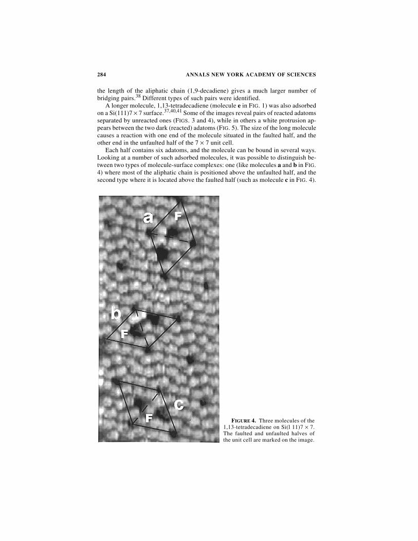
A longer molecule, 1,13-tetradecadiene (molecule e in FIG. 1) was also adsorbedon a Si(111)7 × 7 surface.37,40,41 Some of the images reveal pairs of reacted adatomsseparated by unreacted ones (FIGS. 3 and 4), while in others a white protrusion ap-pears between the two dark (reacted) adatoms (FIG. 5). The size of the long moleculecauses a reaction with one end of the molecule situated in the faulted half, and theother end in the unfaulted half of the 7 × 7 unit cell.
Each half contains six adatoms, and the molecule can be bound in several ways.Looking at a number of such adsorbed molecules, it was possible to distinguish be-tween two types of molecule-surface complexes: one (like molecules a and b in FIG.4) where most of the aliphatic chain is positioned above the unfaulted half, and thesecond type where it is located above the faulted half (such as molecule c in FIG. 4).
FIGURE 4. Three molecules of the1,13-tetradecadiene on Si(l 11)7 × 7.The faulted and unfaulted halves ofthe unit cell are marked on the image.

285MANASSEN & SHACHAL: SCANNING TUNNELING MICROSCOPY
Looking at the positions of the aliphatic chain in 172 adsorbed molecules, reveals apreference of 2:1 for the chain to reside over the unfaulted half. In both cases oneSi−C−C−Si complex is formed in the faulted half of the unit cell, while the secondSi−C−C−Si is formed in the unfaulted half. In addition, counting all the possibleways in which the molecule can be bound to the Si(111)7 × 7 unit cell gives equalnumber of configurations in which the aliphatic chain resides either above the fault-ed or the unfaulted half.
It was thus clear that there is a certain noncovalent interaction between the ali-phatic chain and the 7 × 7 unit cell which is different in the two halves of the cell.We have made a calculation based on a molecular modeling program42 to evaluatethe energy of an aliphatic chain located 2.5 Å above either of the two halves of the7 × 7 unit cell. The calculation was simplified by the possibility of representing eachhalf by partial charges at the positions of the dangling bond as was shown by Brom-mer and colleagues.43 We found that the difference in the effective electrostatic in-teraction between the chain and either of the two halves was 30 kcal/mol.
The electrostatic-noncovalent interaction with the surface leads to the preferenceof the molecule to adsorb on the Si(111)7 × 7 unit cell such that a larger fraction ofthe chain is physisorbed above the unfaulted half.41
The white protrusion that appears between the dark reacted adatoms (FIG. 5) inmany of the images40 can only be interpreted as an additional channel for tunneling,due to the presence of the aliphatic chain–through bond tunneling. The height of theprotrusion is 0.4–0.7 Å. On Si(111)7 × 7 at bias voltage of 2 V and current of 1 nA,the transmission (exp[−2κd ] ) is 1.2 × l0−5,44 which corresponds to a resistance ofthe order of 109 Ω. The size of the protrusion measured in the experiment corre-sponds to an increase of the transmission of 1.4 × l0−5 − 3.2 × 10−5.40 From the the-oretical point of view, through bond tunneling is treated as a tunneling problem witha potential barrier with one or more potential wells. However this observation mayalso be linked to the question of the conductance of a single molecule. We recall thatthere have recently been several studies that investigated both theoretically and ex-perimentally the question of the conductance of molecules.45–48 In one of theseworks, the conductance of a single C60 molecule adsorbed onto a gold surface wasmeasured. In this work the tip was accurately positioned such that an electrical con-tact was made. The measured resistance was 55 MΩ. Within certain limits of the tipsample bias (−0.2 to 0.2 V) the STM tip-C60-molecule-surface tunnel junction obeysOhm’s law.46 A theoretical work,48 which calculated the conductance of a single al-kane molecule connecting two gold electrodes, came out with a value of transmis-sion of 10−12 for an alkane with 18 carbon atoms, and of 10−8 for an alkane of 10carbon atoms. The abovementioned experimental observation33 on through bondelectron transfer verified that the transmission probability decreases one order ofmagnitude for each two C−C bonds. This is in agreement with the theoretical results.Although the calculation for the electron transmission through one methylene groupwas not performed, an extrapolation of the results of this calculation should give atransmission of the order of 10−3. This, together with the measured resistance of theC60 molecule, leads to the conclusion that the largest factor in the resistance of thetip-chain-surface junction is actually at the tip-chain and the chain-surface interfac-es, and not the resistance of the chain itself. By decreasing the tip molecule distanceit should be possible to reach the limit where the current is determined only by the

286 ANNALS NEW YORK ACADEMY OF SCIENCES
molecular conductance in a similar way as the conductance of the C60 molecules wasmeasured by point contact.
As can be seen from the figures, not all the molecules give the white protrusionwhich is a result of through bond tunneling. (In FIGURE 5, molecule d does not havesuch a protrusion). The spatial distribution of the molecules with and without a pro-trusion is random (namely, tip switching effects are excluded). The appearance anddisappearance of the protrusion is due to some local characteristics of the surface im-aged. A possible explanation is that since the transmission probability in throughbond tunneling is strongly dependent on the orientation of the mediating group andsince the limited freedom of the chain creates small fluctuations in the orientation ofthe aliphatic chain relative to the tunneling electrons, this may lead to a random vari-ation of the transmission probability and to the appearance and disappearance of thewhite protrusion in a random sequence.
It should be emphasized that the long-range decay of the transmission probabilityof through bond tunneling (as compared with vacuum tunneling) put a principle sig-nificant limitation on the resolution which can be achieved in STM molecular imag-ing when performed in the constant current mode. The slower the decay, the lesserwill be the resolution. For this reason, better results might be observed many timeswhen the STM is operated at the constant height mode when the contrast is based onthe difference in conductance of the chemical groups (for example, an aromaticgroup compared with an alkyl group).
POSSIBLE APPLICATIONS FOR MOLECULAR ELECTRONICS
The capability to immobilize a certain well-defined group (unreacted) on the sur-face might open new possibilities for the field of molecular electronics.49,50 Any realmolecular device of the future will most probably be made from a “smart” molecule
FIGURE 5. Si(111)7 × 7 + 1,13-tetradecadiene.

287MANASSEN & SHACHAL: SCANNING TUNNELING MICROSCOPY
on a surface when the flow of information to and from the molecule will be con-trolled by an STM system. Molecules may serve as wires, switches, rectifiers, andmemory elements for data storage. However, in order to create a functioning device,the different groups were brought together in a supermolecular assembly. This ap-proach, however, has serious control problems. A possible different approach is theincorporation of the different functions on a single molecule. (The more functions,the better). These may include functions for surface binding, molecular transmis-sion, rectification, etc. For this approach, the capability to immobilize different un-reacted functional groups on an atomic resolution surface has several seriousadvantages. The assignment of the exact position of the chemical groups is straight-forward. The tip could be used to study and exploit their electronic properties sepa-rately.
We foresee the future steps in this direction as follows: (1) It will be possible toverify whether the contrast of different chemical groups observed in STM molecularimaging of molecular monolayers is indeed correct also in the same chemical groupswhen they are physisorbed on the surface in isolated immobilized molecules. (2) Weshall investigate incoherent electron transfer through different chemical groups andthe dependence on different parameters such as the distance from or the size and theelectronegativity of the electron acceptor which is immobilized on the chain. (3) Wehope that it will be possible to measure the electrical resistance of different function-al groups. This observation could be reliable, since the molecule is both physisorbedand immobilized on the surface. By arriving to point contact between the tip and themolecule, and between the molecule and the surface, the resistance can be measuredand may be a sensitive finger print to the identity of the group. By immobilizingelectron acceptors and molecular switches51 on the chain it may be possible to in-vestigate their electrical properties.
ACKNOWLEDGMENTS
This work was supported by the Minerva Foundation, Munich, Germany and theBasic Research Foundation administered by the Israeli Academy of Sciences andHumanities. One of us (Y.M.) is an incumbent of the Lilian and George Lyttle Ca-reer Development Chair.
REFERENCES
1. AVOURIS, P. & R. WOLKOW. 1988. Phys. Rev. Lett. 60: 1049.2. AVOURIS, P., I.W. Lio & F. J. Bozso. 1991. J. Vac. Sci. Technol. B 9: 424.3. PELZ , J.P. & R.H. KOCH. 1991. J. Vac Sci. Technol. B 9: 774.4. STROSCIO, J.A., R.M. FEENSTRA & A.P. FEIN. 1987. Phys. Rev. Lett. 58: 1668.5. WAND, T.A., T. MICHELY, R.J. BEHM, C. HEMMINGER & G. COMSA. 1991. Appl.
Phys. A 53: 414.6. HALLMARK,V.M., S. CHIANG, J.K. BROWN & CH. WÖLL. 1991. Phys. Rev. Lett. 66:
48.7. HALLMARK, V.M., S. CHIANG, K.P. MEINHART, & K. HAFNER. 1993. Phys. Rev.
Lett. 70: 3740.8. LIPPEL, P.H., R.J. WILSON, M.D. MILLER, CH. WÖLL & S. CHIANG. 1989. Phys. Rev.
Lett. 62: 171.

288 ANNALS NEW YORK ACADEMY OF SCIENCES
9. OHTANI, H., R.J. WILSON, S. CHIANG & C.M. MATE. 1988. Phys. Rev. Lett. 60:2398.
10. DELAMARCHE, E. & B. MICHEL. 1996. Thin Solid Films 273: 54.11. WALBA, D.M., F. STEVEN, D. C. PARKS & M. D. WAND. 1995. Science 267: 1144.12. PATRICK, D.L., V. J. CEE & T. P. BEEBE, JR. 1994. Science 265: 231.13. STRANICK, S.J., M.N. KAMNA & P.S. WEISS. 1994. Science 266: 99.14. NEJOH, H. 1990. Appl. Phys. Lett. 57: 2907.15. SMITH, D.P.E., J. K.H. HORBER, G. BINNIG & H. NEJOH. 1990. Nature 344: 41. 16. MCGONICAL, G.C., R.H. BERNHARD, Y.H. YEO & D.J. J. THOMSON. 1991. J. Vac.
Sci. Technol. B 9: 1107.17. RABE , J. P. & S. BUCHHOLZ. 1991. Science 257: 424.18. VENKATARAMAN, B., G.W. FLYNN, J. L. WILBUR, J. P. FOLKERS & G.M. WHITE-
SIDES. 1995. J. Phys. Chem. 99: 8684.19. RABE, J.P., S. BUCHHOLZ & L. ASKASKAYA. 1993. Synth. Met. 54: 339.20. TAKEUCHI, H., S. KAWAUCHI & A. AKAI. 1996. Jpn. J. Appl. Phys. 35: 3754.21. SPONG, J. K., H.A. MIZES, L.A. LACOMB, JR., M.M. DOVEK, J.E. FROMMER & J. S.
FOSTER. 1989. Nature 338: 137.22. HORBER, J. K.H., C.A. LANG, T.W. HENSCH, W.M. HECKL & H. MOHWALD. 1988.
Chem. Phys. Lett. 145: 151.23. MICHEL, B., G. TRAVAGLINI, H. ROHRER, C. JOACHIM & M. AMEREIN. 1989. Z
Phys. B 76: 99.24. JOACHIM, CH. & P. SAUTET. 1990. In Scanning Tunneling Microscopy and Related
Methods, R.J. Behm, N. Garcia & H. Rohrer, Eds. Kluwer. Dordrecht.25. EIGLER, D.M., P.S. WEISS, E.E. SCHWEIZER & N.D. LANG. 1991. Phys. Rev. Lett.
66: 1189.26. MARCUS, R.A. 1956. J. Chem. Phys. 24: 966.27. HOPFIELD, J. J. 1974. Proc. NatI. Acad. Sci. USA 71: 3640.28. BERATAN, D.N., J. N. ONUCHIC & J. J. HOPFIELD. 1985. J. Chem. Phys. 83: 5325.29. BERATAN, D.N., J. N. ONUCHIC & J. J. HOPFIELD. 1987. J. Chem. Phys. 86: 4488.30. DIESENHOFFER, J., 0. EPP, K. MIKI, R. HUBER & H. MICHL. 1985. Nature 318: 618.31. HOFFMANN, R. 1973. Acc. Chem. Res. 4: 1.32. LELAND, B.A., A.D. JORAN, P.M. FELKER, J. J. HOPFIELD, A.H. ZEWAIL & P.B. DER-
VAN. 1985. J. Phys. Chem. 89: 5571.33. CLOSS, G.L., L.T. CALCATERRA, N. J. GREEN, R.W. PENFIELD & J. R. MILLER. 1986.
J. Phys. Chem. 90: 3673.34. OHTA, K., G.L. CLOSS, K. MOROKUMA & N. J. GREEN. 1986. J. Am. Chem. Soc.
108: 1319.35. PAULSON, B.P., L.A. CURTISS, G. BAL, G.L. CLOSS & J. R. MILLER. 1996. J. Am.
Chem. Soc. 118: 376.36. PIANCASTELLI, M.N., N. MOTTA, A. SGARLATA, A. BALZAROTTI & M.DE. CRES-
CENZI. 1993. Phys. Rev. B 48: 17892.37. SHACHAL, D., Y. MANASSEN & E. TER-OVANESYAN. 1997. Phys. Rev. B 55: 9367.38. SHACHAL, D. & Y. MANASSEN. 1997. J. Vac. Sci. Technol. B 15: 1310.39. PARK, S.-I. & C.F. QUATE. 1987. Rev. Sci. Instrum. 58: 2004.40. SHACHAL, D. & Y. MANASSEN. 1997. Chem. Phys. Lett. 271: 107.41. SHACHAL, D. & Y. MANASSEN. 1998. Appl. Phys. A. 66: S1229.42. [Insight 11, Biosym Technologies, San Diego]43. BROMMER, K.D., M. GALVAN, A. DAL PINO, JR. & J. P. JOANNOPOULUS. 1994. Surf.
Sci. 314: 57.44. CHEN, C.J. & R.J. HAMERS. 1991. J. Vac. Sci. TechnoL B 9: 503.45. BUNN, L.A., J. J. ARNOLD, M.T. CYGAN, T.D. DUNBAR, T.P. BURGIN, L. GONES,
D.L. ALLARA & P.S. WEISS. 1995. Science 271: 1705.

289MANASSEN & SHACHAL: SCANNING TUNNELING MICROSCOPY
46. JOACHIM, C., J. K. GIMZEWSKI, R. SCHLITTER & C. CHAVY. 1995. Phys. Rev. Lett.74: 2102.
47. JOACHIM, C. & J. K. GIMZEWSKI. 1995. Europhys. Lett. 30: 409.48. JOACHIM, C. & J.F. VINUESA. 1996. Europhys. Lett. 33: 635.49. AVIRAM, A. & M.A. RATNER. 1974. Chem. Phys. Lett. 29: 277.50. AVIRAM, A. 1992. Int. J. Ouan. Chem. 42: 1615.51. FARAZDEL, A., M. DUPUIS, E. CLEMENTI & A. AVIRAM. 1990. J. Am. Chem. Soc.
112: 4206.