Embed Size (px)
Citation preview

SCANNING PROBE MICROSCOPY

SCANNING PROBEMICROSCOPY
ELECTRICAL ANDELECTROMECHANICALPHENOMENA AT THENANOSCALEVolume II
Sergei KalininAlexei GruvermanEditors

Sergei KalininOak Ridge National LaboratoryOak Ridge, TN, 37831USAsergei2.kalininweb.com
Alexei GruvermanDept. Materials Science and EngineeringNorth Carolina State UniversityRaleigh, NC, 27695USAalexei [email protected]
Library of Congress Control Number: 2006926451
ISBN-10: 0-387-28667-5 e-ISBN-10: 0-387-28668-3ISBN-13: 978-0387-28667-9 e-ISBN-13: 978-0387-28668-6
Printed on acid-free paper.
C© 2007 Springer Science+Business Media, LLCAll rights reserved. This work may not be translated or copied in whole or in part without the writtenpermission of the publisher (Springer Science+Business Media, LLC, 233 Spring Street, New York,NY 10013, USA), except for brief excerpts in connection with reviews or scholarly analysis. Usein connection with any form of information storage and retrieval, electronic adaptation, computersoftware, or by similar or dissimilar methodology now known or hereafter developed is forbidden.The use in this publication of trade names, trademarks, service marks, and similar terms, even if theyare not identified as such, is not to be taken as an expression of opinion as to whether or not they aresubject to proprietary rights.
9 8 7 6 5 4 3 2 1
springer.com

Contents
List of Contributors .................................................................. ix
About the Editors ..................................................................... xix
VOLUME II
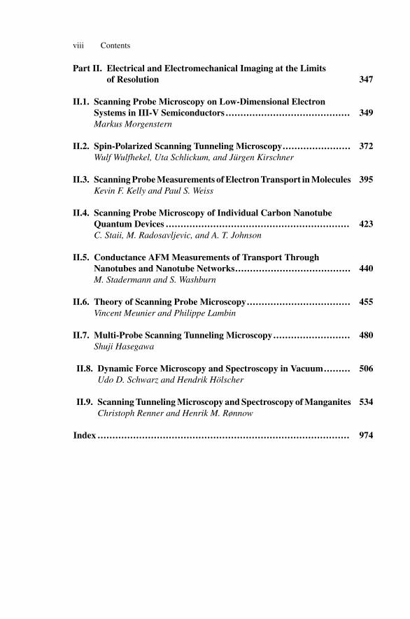
Part III. Electrical SPM Characterization of Materials and Devices 559
III.1. Scanning Voltage Microscopy: Investigating the Inner Workingsof Optoelectronic Devices ................................................... 561Scott B. Kuntze, Dayan Ban, Edward H. Sargent, St. JohnDixon-Warren, J. Kenton White, and Karin Hinzer
III.2. Electrical Scanning Probe Microscopy of Biomoleculeson Surfaces and at Interfaces .............................................. 601Ida Lee and Elias Greenbaum
III.3. Electromechanical Behavior in Biological Systemsat the Nanoscale ............................................................... 615A. Gruverman, B. J. Rodriguez, and S. V. Kalinin
III.4. Scanning Capacitance Microscopy: Applications in FailureAnalysis, Active Device Imaging, and Radiation Effects............ 634C. Y. Nakakura, P. Tangyunyong, and M. L. Anderson
III.5. Kelvin Probe Force Microscopy of Semiconductors ................. 663Y. Rosenwaks, S. Saraf, O. Tal, A. Schwarzman, Th. Glatzel,and M.Ch. Lux-Steiner
v

vi Contents
III.6. Nanoscale Characterization of Electronic and ElectricalProperties of III-Nitrides by Scanning Probe Microscopy ......... 690B. J. Rodriguez, A. Gruverman, and R. J. Nemanich
III.7. Electron Flow Through Molecular Structures ........................ 715Sidney R. Cohen
III.8. Electrical Characterization of Perovskite Nanostructuresby SPM .......................................................................... 746K. Szot, B. Reichenberg, F. Peter, R. Waser, and S. Tiedke
III.9. SPM Measurements of Electric Properties of Organic Molecules 776Takao Ishida, Wataru Mizutani, Yasuhisa Naitoh, and HiroshiTokumoto
III.10. High-Sensitivity Electric Force Microscopy of OrganicElectronic Materials and Devices ....................................... 788William R. Silveira, Erik M. Muller, Tse Nga Ng, David H. Dunlap,and John A. Marohn
Part IV. Electrical Nanofabrication 831
IV.1. Electrical SPM-Based Nanofabrication Techniques................ 833Nicola Naujoks, Patrick Mesquida, and Andreas Stemmer
IV.2. Fundamental Science and Lithographic Applicationsof Scanning Probe Oxidation............................................. 858J. A. Dagata
IV.3. UHV-STM Nanofabrication on Silicon ................................ 880Peter M. Albrecht, Laura B. Ruppalt, and Joseph W. Lyding
IV.4. Ferroelectric Lithography................................................. 906Dongbo Li and Dawn A. Bonnell
IV.5. Patterned Self-Assembled Monolayers via ScanningProbe Lithography.......................................................... 929James A. Williams, Matthew S. Lewis, and Christopher B. Gorman
IV.6. Resistive Probe Storage: Read/Write Mechanism .................. 943Seungbum Hong and Noyeol Park

Contents vii
VOLUME I
Introduction: Scanning Probe Microscopy Techniques for Electricaland Electromechanical Characterization ....................................... 1S. V. Kalinin and A. Gruverman
Part I. SPM Techniques for Electrical Characterization 9
I.1. Scanning Tunneling Potentiometry: The Power of STM appliedto Electrical Transport......................................................... 11A. P. Baddorf
I.2. Probing Semiconductor Technology and Devices with ScanningSpreading Resistance Microscopy .......................................... 31P. Eyben, W. Vandervorst, D. Alvarez, M. Xu, and M. Fouchier
I.3. Scanning Capacitance Microscopy for ElectricalCharacterization of Semiconductors and Dielectrics .................. 88J. J. Kopanski
I.4. Principles of Kelvin Probe Force Microscopy............................ 113Th. Glatzel, M.Ch. Lux-Steiner, E. Strassburg, A. Boag,and Y. Rosenwaks
I.5. Frequency-Dependent Transport Imaging by ScanningProbe Microscopy ............................................................... 132Ryan O’Hayre, Minhwan Lee, Fritz B. Prinz, and Sergei V. Kalinin
I.6. Review of Ferroelectric Domain Imaging by PiezoresponseForce Microscopy.............................................................. 173A. L. Kholkin, S. V. Kalinin, A. Roelofs, and A. Gruverman
I.7. Principles of Near-Field Microwave Microscopy ...................... 215Steven M. Anlage, Vladimir V. Talanov, and Andrew R. Schwartz
I.8. Electromagnetic Singularities and Resonances in Near-FieldOptical Probes .................................................................. 254Alexandre Bouhelier and Renaud Bachelot
I.9. Electrochemical SPM: Fundamentals and Applications............. 280T. J. Smith and K. J. Stevenson
I.10. Near-Field High-Frequency Probing ..................................... 315C. A. Paulson and D. W. van der Weide
viii Contents
Part II. Electrical and Electromechanical Imaging at the Limitsof Resolution 347
II.1. Scanning Probe Microscopy on Low-Dimensional ElectronSystems in III-V Semiconductors .......................................... 349Markus Morgenstern
II.2. Spin-Polarized Scanning Tunneling Microscopy....................... 372Wulf Wulfhekel, Uta Schlickum, and Jurgen Kirschner
II.3. Scanning Probe Measurements of Electron Transport in Molecules 395Kevin F. Kelly and Paul S. Weiss
II.4. Scanning Probe Microscopy of Individual Carbon NanotubeQuantum Devices .............................................................. 423C. Staii, M. Radosavljevic, and A. T. Johnson
II.5. Conductance AFM Measurements of Transport ThroughNanotubes and Nanotube Networks....................................... 440M. Stadermann and S. Washburn
II.6. Theory of Scanning Probe Microscopy................................... 455Vincent Meunier and Philippe Lambin
II.7. Multi-Probe Scanning Tunneling Microscopy .......................... 480Shuji Hasegawa
II.8. Dynamic Force Microscopy and Spectroscopy in Vacuum......... 506Udo D. Schwarz and Hendrik Holscher
II.9. Scanning Tunneling Microscopy and Spectroscopy of Manganites 534Christoph Renner and Henrik M. Rønnow
Index ..................................................................................... 974

List of Contributors
Peter M. AlbrechtBeckman Institute405 N. MathewsUrbana, IL 61801Phone: 217-244-1058Fax: 217-244-1995E-mail: [email protected]
David AlvarezInfineon Technologies05452 Essex Junction, VT, USAPhone: 1-802-769-4904E-mail: [email protected]
Dr. Meredith L. AndersonSandia National LaboratoriesP.O. Box 5800, MS1077Albuquerque, NM 87185-1077E-mail: [email protected]
Prof. Steven M. AnlageCenter for Superconductivity
ResearchDepartment of PhysicsUniversity of MarylandCollege Park, MD 20742-4111, USAPhone: +001 301 405 7321Fax: +001 301 405 3779E-mail: [email protected]://www.csr.umd.edu
Dr. Arthur P. BaddorfOak Ridge National Laboratory1 Bethel Valley Road, Bldg. 3025Oak Ridge, TN 37831-6030Phone: (865) 574-5241Fax: (865) 574-4143E-mail: [email protected]://nanotransport.ornl.gov
Prof. R. BachelotLaboratoire de Nanotechnologieet d’Instrumentation OptiqueInstitut Charles Delaunay
CNRS-FRE 2848Universite de Technologie de
TroyesF-10010 Troyes, FranceE-mail: [email protected]
Dayan BanUniversity of WaterlooDepartment of Electrical and
Computer Engineering200 University Ave. WestWaterloo, Ontario
A. BoagFaculty of EngineeringTEL-AVIV UNIVERSITYTel-Aviv 69978, ISRAEL
ix

x List of Contributors
Prof. Dawn A. BonnellDepartment of Materials Science and
EngineeringThe University of Pennsylvania3231 Walnut Street, Philadelphia PA
19104Phone: 215 898 6231Fax: 215 573 2128E-mail: [email protected]
Dr. Alexandre BouhelierLaboratoire de Physique de
l’Universite de BourgogneUMR 5027Faculte des Sciences Mirande—9
Avenue Alain SavaryB.P. 47 870—F-21078 DIJON
Cedex—FRANCEE-mail: alexandre.bouhelier@u-
bourgogne.fr
Dr. Sidney R. CohenDirector, Surface Analysis LaboratoryChemical Research SupportWeizmann Institute of ScienceRehovot 76100 ISRAELPhone: 972 8 934 2703Fax: 972 8 934 4137E-mail: [email protected]://www.weizmann.ac.il/Chemical
Research Support/surflab/
Dr. John A. DagataPrecision Engineering DivisionNational Institute of Standards &
Technology100 Bureau Drive MS 8212Gaithersburg MD 20899-8212 USAPhone: 301-975-3597Fax: 301-869-0822E-mail: [email protected]
Dr. St. J. Dixon-WarrenChipworks3685 Richmond Road, Suite 500Ottawa, Ontario, Canada
Prof. David DunlapDept. of Physics and AstronomyUniv. of New MexicoAlbuquerque, NM 87131Phone: (505) 277-2120Fax: (505) 277-1520E-mail: [email protected]
Dr. P. EybenKapeldreef 75, B-3001Leuven, BelgiumPhone: 32 16 281 305E-mail: [email protected]
Dr. Marc FouchierVeeco instruments S.A.S.Z .I. de la Gaudree—11 rue Marie
PoussepinBP 43—91412 Dourdan—FrancePhone: +33 (0)6 24 60 19 23E-mail: [email protected]
Dr. Thilo GlatzelInstitute of Physics, University of
BaselKlingelbergstr. 82CH-4056 BaselPhone: +41(0)61 267-3730Fax: +41(0)61 267-3795E-mail: [email protected]://www.physik.unibas.ch
Prof. Christopher GormanDepartment of ChemistryNorth Carolina State University314 Dabney HallRaleigh, NC 27695-8204Phone: 919-515-4252Fax: 919-515-8920E-mail: Chris [email protected]
Dr. Elias GreenbaumChemical Sciences DivisionOak Ridge National LaboratoryOak Ridge, TN 37831 USA
List of Contributors xi
Phone: 865-574-6835Fax: 865-574-1275E-Mail: [email protected]
Prof. Alexei GruvermanDepartment of Materials Science and
EngineeringNorth Carolina State UniversityRaleigh, NC 27695, USAPhone: +1 (919) 5133319Fax: +1 (919) 5157724E-mail: Alexei [email protected]
Prof. S. HasegawaDepartment of PhysicsSchool of Science University of Tokyo7-3-1 Hongo, Bunkyo-ku, Tokyo
113-0033, JAPANPhone/Fax +81-3-5841-4167E-mail:[email protected]
Dr. K. HinzerBookham10 Brewer Hunt WayOttawa, Ontario
Dr. Hendrik HolscherCenter for NanoTechnology
(CeNTech)University of MuensterGievenbecker Weg 1148149 Muenster, GermanyPhone: +49 (0) 251 83-63832Fax: +49 (0) 251 83 -63873E-mail:[email protected]://www.uni-muenster.de/nanoforce
Dr. Seungbum HongSemiconductor Device and Material
LabSamsung Advanced Institute of
TechnologyP.O. Box 111, Suwon 440-600, KoreaE-mail: [email protected]
Dr. Takao IshidaNanotechnology Research Institute
(NRI),National Institute of Advanced
Industrial Science and Technology(AIST)
1-1-1 Higashi, Tsukuba, Ibaraki305-8562, Japan
Phone: +81-29-861-7203,Fax: +81-29-861-2786E-mail: [email protected]
Prof. A.T. Charlie Johnson, JrDepartment of Physics and AstronomyUniversity of Pennsylvania,209 S. 33rd St., Philadelphia PA
19104-6396Phone: (215) 898-9325Fax: (215) 898-2010Email: [email protected]
Dr. Sergei V. KalininMaterials Sciences and Technology
Division and Center for NanophaseMaterials Sciences
Oak Ridge National Laboratory1 Bethel Valley RdBldg. 3025, MS6030Oak Ridge, TN 37831Phone: (865) 241-0236Fax: (865) 574-4143E-mail: [email protected]
Prof. Kevin F. KellyECE Dept., MS-366Rice UniversityPO Box 1892Houston, TX 77005-1892Phone: 713-348-3565Fax: 713-348-5686E-mail: [email protected]
Dr. Andrei KholkinDepartment of Ceramics and Glass
Engineering &

xii List of Contributors
Center for Research in Ceramic andComposite
Materials (CICECO), University ofAveiro
3810-193 Aveiro, PortugalPhone: +351 234370235Fax: +351 234425300E-mail: [email protected]
Prof. Jurgen KirschnerMax-Planck Institut fur
MikrostrukturphysikWeinberg 206120 HalleGermanyPhone: +49-345-5582656Fax: +49-345-5511223E-mail: [email protected]
J.J. KopanskiNational Institute of Standards and
TechnologySemiconductor Electronics Division100 Bureau Dr., stop 8120Gaithersburg, MD 20899-8120E-mail: [email protected]
Prof. Philippe LambinFUNDPRue de Bruxelles 61B-5000 Namur, Belgium
S. B. KuntzeUniversity of TorontoDepartment of Electrical and
Computer Engineering10 King’s College Rd.Toronto, Ontario
Dr. Ida LeeOak Ridge National Laboratory1 Bethel Valley RoadPO Box 2008Building 4500N, MS 6194, Room A8Oak Ridge, TN 37831
Phone: 865-241-6695 or 865-574-6183Fax: 865-574-1275E-Mail: [email protected]
Minhwan LeeStanford UniversityDepartment of Mechanical
Engineering440 Escondido MallBuilding 530, Room 226Stanford, CA. 94305Phone: 650-723-6488Fax: 650-723-5034
M. LewisDepartment of ChemistryNorth Carolina State University314 Dabney HallRaleigh, NC 27695-8204
Dongbo LiDepartment of Materials Science and
EngineeringThe University of Pennsylvania3231 Walnut Street, Philadelphia, PA
19104Phone: 215 898 3446Fax: 215 573 2128E-mail: [email protected]
Prof. Dr. Martha Ch. Lux-SteinerDepartment of Heterogeneous
Material Systems (SE2)Hahn-Meitner-Institut BerlinGlienicker Str. 100 D-14109 BerlinFon: +49 30 8062-2462Fax: +49 30 8062-3199Email: [email protected]
Prof. Joseph W. LydingBeckman Institute405 N. MathewsUrbana, IL 61801Phone: 217-333-8370Fax: 217-244-1995E-mail: [email protected]
List of Contributors xiii
Prof. John A. MarohnDept. of Chemistry and Chemical
Biology150 Baker LaboratoryCornell UniversityIthaca, NY 14853-1301Phone: 607-255-2004Fax: 607-255-4137E-mail: [email protected]
Dr. Patrick MesquidaDivision of EngineeringKing’s College LondonStrand, London WC2R 2LSPhone: +44 (0)20 7848 2241Fax: +44 (0)20 7848 2932E-mail: [email protected]
Dr. Vincent MeunierComputer Science and Mathematics
Division& Center of Nanophase MaterialsSciencesOak Ridge National Laboratory1 Bethel Valley Rd.Oak Ridge, TN 37831E-mail: [email protected]
Dr. Wataru MizutaniNanotechnology Research Institute
(NRI)National Institute of Advanced
Industrial Science and Technology(AIST)
1-1-1 Higashi, Tsukuba,Ibaraki 305-8562, Japan
Phone: +81-29-861-2434Fax: +81-29-861-2786E-mail: [email protected]
Dr. Markus MorgensternII. Inst. of Physics BRWTH Aachen UniversityD-52056 Aachen, GermanyPhone: (++)49-241-80-27075/6
Fax: (++)49-241-80-22306E-mail:
E.M. MullerDept. of Chemistry and Chemical
Biology150 Baker LaboratoryCornell UniversityIthaca, NY 14853-1301
Dr. Yasuhisa NaitohNanotechnology Research Institute
(NRI)National Institute of Advanced
Industrial Science and Technology(AIST)
1-1-1 Higashi, Tsukuba,Ibaraki 305-8562, Japan
Phone: +81-29-861-7892Fax: +81-29-861-2786E-mail: [email protected]
Dr. Craig Y. NakakuraSandia National LaboratoriesP.O. Box 5800, MS1077Albuquerque, NM 87185-1077E-mail: [email protected]
Dr. Nicola NaujoksNanotechnology GroupETH ZurichTannenstrasse 3CH-8092 Zurich, SwitzerlandPhone: +41 44 632 69 89Fax: +41 44 632 12 78E-mail: [email protected]://www.nanotechnology.ethz.ch
Prof. Robert J. NemanichDepartment of PhysicsNorth Carolina State UniversityRaleigh, NC 27695-8202Phone: (919) 515-3225Fax: (919) 515-7331

xiv List of Contributors
E-mail: Robert [email protected]
T.N. NgDept. of Chemistry and Chemical
Biology150 Baker LaboratoryCornell UniversityIthaca, NY 14853-1301
Prof. Ryan O’HayreColorado School of MinesDepartment of Metallurgical and
Materials Engineering1500 Illinois St.Golden, CO. 80401Phone: 303-273-3770Fax: 303-273-3795
Dr. Charles PaulsonDepartment of Electrical Engineering1415 Engineering Dr.Madison, WI 53706E-mail: [email protected]
Mr. Noyeol ParkVice PresidentStorage System DivisionSemiconductor BusinessSamsung ElectronicsSuwon, Korea
Dr. Frank PeterResearch Center Juelich52425 Juelich, GermanyPhone: +492461616479E-mail: [email protected]
Prof. Fritz PrinzStanford UniversityDepartment of Mechanical
Engineering440 Escondido MallBuilding 530, Room 226Stanford, CA. 94305
Phone: 650-723-6488Fax: 650-723-5034
Dr. Marko RadosavljevicComponents ResearchIntel Corporation, RA3-2525200 NE Elam Young ParkwayHillsboro, OR 97124Phone: 503-613-4732E-mail:
Dr. Bernd ReichenbergaixACCT Systems GmbHDennewartstrasse 25-2752068 Aachen, GermanyE-mail: [email protected]
Dr. Christoph RennerLondon Centre for Nanotechnology
and Department of Physics andAstronomy
University College LondonGordon Street 17-19London WC1E 6BT, UKPhone: +44 (0)20 7679 3496Fax: +44 (0)20 7679 1360E-mail: [email protected]://www.cmmp.ucl.ac.uk/∼cr/
Dr. Andreas RoelofsSeagate Technology1251 Waterfront PlacePittsburgh, PA 15222, USAPhone: +1 (412) 918 7028Fax (412) 918 7222E-mail:
Dr. Brian J. RodriguezMaterials Science and Technology
DivisionOak Ridge National Laboratory1 Bethel Valley RdBldg. 3137, MS6057

List of Contributors xv
Oak Ridge, TN 37831Phone: (865) 574-0791Fax: (865) 576-8135E-mail: [email protected]
Dr. Henrik M. RønnowLaboratory for Neutron ScatteringETH-Zurich & Paul Scherrer
Institute5232 VilligenSwitzerlandPhone: +41 56 310 4668Fax: +41 56 310 2939E-mail: [email protected]
Prof. Yossi RosenwaksFaculty of EngineeringElec. Lab. Building, room 231TEL-AVIV UNIVERSITYTel-Aviv 69978, ISRAELPhone: +972-3-6406248Fax: +972-3-6423508E-mail: [email protected]://www.eng.tau.ac.il/∼yossir/
rosenwaks.html
Laura B. RuppaltBeckman Institute405 N. MathewsUrbana, IL 61801Phone: 217-244-5665Fax: 217-244-1995E-mail: [email protected]
S. SarafFaculty of EngineeringTEL-AVIV UNIVERSITYChemical DepartmentTel-Aviv 69978, ISRAELE-mail: mailto:[email protected]
Prof. E.H. SargentUniversity of TorontoDepartment of Electrical and
Computer Engineering
10 King’s College Rd.Toronto, Ontario
Dr. Uta SchlickumInstitut de Physique des
NanostructuresEPFL/SB/IPN, PHB-Ecublens,
Station 3CH-1015 LausanneSwitzerlandPhone: +41 (0)21 69 34 742Fax: +41 (0)21 69 33 604E-mail: [email protected]
Dr. Andrew R. SchwartzNeocera Inc.10000 Virginia Manor RoadBeltsville, MD 20705, USAPhonr: +001 301 210 1010Fax: +001 301 210 1042E-mail: [email protected]://www.neocera.com
Prof. Udo D. SchwarzDepartment of Mechanical
EngineeringYale UniversityP.O. Box 208284New Haven, CT 06520-8284USAPhone: +1-203-432-7525Fax: +1-203-432-6775E-mail: [email protected]://www.eng.yale.edu/nanomechanics
A. SchwarzmanFaculty of EngineeringTEL-AVIV UNIVERSITYTel-Aviv 69978, ISRAEL
W.R. SilveiraDept. of Chemistry and Chemical
Biology150 Baker LaboratoryCornell UniversityIthaca, NY 14853-1301

xvi List of Contributors
Timothy J. SmithDepartment of Chemistry and
BiochemistryUniversity of Texas at Austin1 University Station/MC A5300Austin, TX 78712E-mail: [email protected]
Dr. Michael StadermannL-234Chemistry & Material ScienceLawrence Livermore National
Laboratory7000 East AveLivermore, Ca 94550
Dr. Cristian StaiiDepartment of ChemistryPrinceton UniversityPrinceton, NJ 08544Phone: 609 258-3962E-mail: [email protected]
Prof. Andreas StemmerNanotechnology GroupETH ZurichTannenstrasse 3CH-8092 ZurichSWITZERLANDPhone: +41 44 632 4572Fax: +41 44 632 1278E-mail: [email protected]
Prof. Keith StevensonDepartment of Chemistry and
BiochemistryUniversity of Texas at Austin1 University Station/MC A5300Austin, TX 78712Phone: (512)232-9160E-mail:
E. StrassburgFaculty of Engineering
TEL-AVIV UNIVERSITYTel-Aviv 69978, ISRAEL
Prof. Kristof SzotInstitute of Physics, University of
Silesia40-007 Katowice, Polandand Research Center Juelich52425 Juelich, GermanyPhone: +492461616479email: [email protected]
O. TalFaculty of EngineeringTEL-AVIV UNIVERSITYTel-Aviv 69978, ISRAEL
Dr. Vladimir V. TalanovNeocera Inc.10000 Virginia Manor RoadBeltsville, MD 20705, USAPhone: +001 301 210 1010Fax: +001 301 201 1042E-mail: [email protected]://www.neocera.com
Dr. Paiboon TangyunyongSandia National LaboratoriesP.O. Box 5800, MS1081Albuquerque, NM 87185-1081E-mail: [email protected]
Dr. Stephan TiedkeaixACCT Systems GmbHDennewartstrasse 25-2752068 Aachen, GermanyPhone: +492419631410E-mail: [email protected]
Prof. Hiroshi TokumotoNanotechnology Research CenterResearch Institute for Electronic
ScienceHokkaido University

List of Contributors xvii
Kita-ku N21 W10, Sapporo 001-002,Japan
Phone:+81-11-706-9354Fax:+81-11-706-9355E-mail: [email protected]
Prof. W. VandervorstKapeldreef 75, B-3001Leuven, Belgiumtel 32 16 281 286E-mail: [email protected]
Prof. Rainer WaserResearch Center Juelich52425 Juelich, GermanyPhone: +492461615811E-mail: [email protected]
Prof. Sean WashburnDept Physics and AstronomyUniv North Carolina at Chapel HillChapel Hill, NC 27599-3255
Prof. Daniel van der WeideDepartment of Electrical & Computer
EngineeringUniversity of Wisconsin1415 Engineering DrMadison WI 53711, USAPhone: 608-265-6561Fax: 815-371-3407E-mail: [email protected]://vdw.ece.wisc.edu
Prof. Paul S. WeissDepartment of Chemistry and Physics
104 Davey LaboratoryThe Pennsylvania State UniversityUniversity Park, PA 16802-6300,
USAPhone: +1 (814) 865-3693Fax: +1 (814) 863-5516E-mail: [email protected]://www.nano.psu.edu/
J.K. WhiteBookham10 Brewer Hunt WayOttawa, Ontario
J. WilliamsDepartment of ChemistryNorth Carolina State University314 Dabney HallRaleigh, NC 27695-8204
Prof. Wulf WulfhekelPhysikalisches InstitutUniversitat KarlsruheWolfgang Gaede Strasse 176131 KarlsruheGermanyPhone: +49-721-6083440Fax: +49-721-6086103E-mail:
Dr. M. XuKapeldreef 75, B-3001Leuven, BelgiumPhone: 32 16 288 024E-mail: [email protected]

About the Editors
Sergei Kalinin is currently a research staffmember at the Oak Ridge National Laboratory,Materials Sciences and Technology Division andCenter for Nanophase Materials Science. Hecompleted his Ph.D. in Materials Science at theUniversity of Pennsylvania in 2002 (with Prof.Dawn Bonnell). His previous undergraduate andgraduate work in Materials Science was con-ducted at Moscow State University, Moscow,Russia. The focus of his current research in-terests is interplay between electromechanical,
transport, and mechanical phenomena in inorganic and biological systems usinglocal probes. He serves as a member of American Vacuum Society NSTD board andmember of editorial board for Journal of Nanoelectronics and Optoelectronics. Asa student, he earned multiple research awards including American Vacuum SocietyGraduate Student Award and several Materials Research Society Graduate StudentAwards. He was recognized with the Ross Coffin Purdy Award of American Ce-ramics Society (2003) for the development of Scanning Impedance Microscopyfor characterization of frequency-dependent transport on the nanoscale. He is alsoa recipient of Wigner Fellowship of Oak Ridge National Laboratory (2002) and anOak Ridge National Laboratory Early Career Accomplishment Award for Scienceand Technology (2005). He has authored more than 70 scientific papers, six bookchapters and five patents on various aspects of SPM.
xix

xx About the Editors
Alexei Gruverman is currently a Research As-sociate Professor in the Department of MaterialScience and Engineering, North Carolina StateUniversity. He received his PhD degree in SolidState Physics from the Ural State University inRussia. After graduation, he worked as a post-doctoral researcher at the Joint Research Centerfor Atom Technology (JRCAT), Japan, where heinitiated a project on scanning probe microscopystudies of ferroelectrics. He then joined SonyCorporation to work on the problems related to
characterization and reliability of ferroelectric memory devices by SPM. In 2000,he joined the faculty at North Carolina State University. He has published over 80articles in refereed journals, several book chapters and edited one book. His cur-rent research interests are in the field of ferroelectric nanostructures and thin films,nanoscale phenomena in ferroic materials, mechanical properties of biomaterialsand non-volatile information storage technologies. He is a recipient of the IkedaAward (2004) for contribution to SPM studies of ferroelectrics.

P1: OTE/SPH P2: OTE
SVNY294-Kalinin August 19, 2006 20:14
IntroductionScanning Probe Microscopy Techniques forElectrical and Electromechanical Characterization
S.V. KALININ AND A. GRUVERMAN
Progress in modern science is impossible without reliable tools for characteriza-tion of structural, physical, and chemical properties of materials and devices atthe micro-, nano-, and atomic scale levels. While structural information can beobtained by such established techniques as scanning and transmission electronmicroscopy, high-resolution examination of local electronic structure, electric po-tential and chemical functionality is a much more daunting problem. Local elec-tronic properties became accessible after the development of Scanning TunnelingMicroscopy by G. Binnig and H. Rohrer in 1981 at IBM Zurich 25 years ago—aninvention that earned its authors the Nobel Prize in Physics five years later [1].Based on the quantum mechanical tunneling between an atomically sharp metallictip and conductive surface, scanning tunneling microscopy (STM) has becomethe first instrument to generate real-space images of surfaces with atomic resolu-tion and has triggered development of new classes of STM-related techniques. In1986, Binnig, Quate, and Gerber demonstrated atomic force microscope (AFM)based on the mechanical detection of the Van der Waals forces between the tipand the surface using a pliable cantilever [2]. It was almost immediately realizedthat AFM could be extended to map forces of various types, such as magneticand electrostatic forces, as well as for probing chemical interactions. This dualcapability of probing currents and forces at the nanometer and atomic level hasled to a rapid growth of a variety of scanning probe microscopy (SPM) techniquesover the last two decades. Techniques such as AFM, magnetic force microscopy(MFM), electrostatic force microscopy (EFM), scanning capacitance microscopy(SCM), near-field scanning optical microscopy (NSOM), and others have emergedto provide capability to access local electrical, magnetic, chemical, mechanical,optical, and thermal properties of materials on the nanometer scale. It has beendemonstrated that the SPM approach allows not only imaging, but also controland modification of the local structure and material functionality at the nano- andatomic level. As a consequence, the last two decades have witnessed an explo-sive growth in application of SPM techniques in a wide spectrum of fields ofscience, ranging from condensed matter physics, chemistry and materials scienceto medicine and biology. It will not be an exaggeration to say that the rapid devel-opment of nanoscience and nanotechnology in the last two decades was strongly
1

P1: OTE/SPH P2: OTE
SVNY294-Kalinin August 19, 2006 20:14
2 Introduction
stimulated by the availability of SPM techniques, and in turn constantly stimulatesdevelopment of novel SPM probes.
In parallel with the development of ambient SPM techniques, a significantprogress was achieved in the development of high-resolution ultrahigh vacuum(UHV) SPM systems. Compared to ambient systems, UHV operation imposesmajor difficulties in the sample preparation and microscope operation. However,it provides a potential for true atomic resolution imaging both in STM and AFMmodes. STM sensitivity to local electronic properties provided physicists with thetool to probe electronic phenomena such as edge states in quantum Hall systems,phase separation and charge ordering in strongly correlated oxides, and transportin mesoscopic conductors. In the context of surface science and catalysis, the ca-pability to probe chemical and photochemical processes on the atomic level haveemerged. Many ambient electrostatic and electromechanical probes can be im-plemented in UHV conditions as well. As such, UHV SPM paves the way to theinvestigation of fundamental electrical and mechanical properties of materials atthe atomic level.
One of the primary challenges in the SPM applications to local electrostaticand electromechanical phenomena is quantitative analysis of the acquired signal.Indeed, a typical SPM image, were it a surface potential map, electromechni-cal activity map, capacitance distribution or a gate potential image, provides aquantitative measure of local surface properties. However, image formation mech-anisms in most SPM techniques are extremely complex due to the geometry of tip-surface system and multitude of contributing interactions. For example, noticeableprogress in understanding such well-established topographic imaging techniquesas non-contact AFM or intermittent contact AFM was achieved only in the last fewyears. The problem of quantitative interpretation of the local property map is evenmore difficult; further progress requires thorough understanding of the image for-mation mechanisms through combination of first-principles methods to describeatomistic processes at tip-surface junction, continuum mechanics, and electrostat-ics to describe long-range interactions and cantilever dynamics. However, onceachieved, this transforms SPM from a mere imaging tool into a quantitative probeof local physical phenomena on the nanoscale, realizing an age-old dream of pre-cise measurements of physical and chemical properties on nanometer, molecular,and ultimately atomic levels.
Tremendous growth in SPM instrumentation, theory, and applications have re-sulted in a large number of monographs, books, and reviews addressing generalaspects of SPM [3–12], including STM studies of atomic structure and electronicphenomena [13–16], electrochemical SPM [17], theoretical aspects of AFM [18]and STM [19], nanofabrication [20], application of SPM in biology and bioengi-neering [21–24]. However, there is a long-due need to bring together a permanentlygrowing knowledge base on the practical and theoretical aspects of advanced elec-trical and electromechanical SPM techniques. The goal of this book is to providea comprehensive reference on the nanoscale characterization of electrical andmechanical properties of functional materials by SPM techniques and to makereaders aware of tremendous developments in the field in the last decade. This
P1: OTE/SPH P2: OTE
SVNY294-Kalinin August 19, 2006 20:14
Introduction 3
book provides a link between well-established ambient SPM techniques and UHVSPM, materials and device applications, and theoretical basis for interpretationof SPM data. While a number of SPM techniques have been used in a varietyof scientific fields ranging from semiconductors to ferroelectrics to optics, in thisbook various aspects of these techniques will be presented on an interdisciplinarybasis. By bringing together critical reviews written by the leading researchers fromthe different scientific disciplines relevant information will be conveyed that willallow readers to learn more about the fundamental and technological advances andfuture trends in the different fields of nanoscience.
The book comprises 35 chapters divided into four parts. Part I introduces thereader to the technical and instrumental features of SPM techniques for elec-trical, electromechanical, transport, near-field optical and microwave characteri-zation. Part II deals with the SPM imaging at the resolution limit in molecularsystems, complex oxides, and low-dimensional structures, as well as theoreticalunderpinnings of SPM. Part III illustrates application of SPM to electrical andelectromechanical characterization of a broad spectrum of materials ranging fromsemiconductors to polymers to biosystems. Finally, Part IV discusses SPM-baseddevices and nanofabrication methods.
Chapter I.01 by A. P. Baddorf reviews technical aspects of Scanning TunnelingPotentiometry (STP), an extension of STM to transport measurements. The chapterdiscusses applications of STP to probe mesoscopic transport in low-dimensionalsystems, defect-induced scattering, and transport tin phase-separated strongly cor-related oxides. Further prospects of transport imaging with nanometer and atomicresolution are discussed. Chapter I.02 by P. Eyben et al., discusses implemen-tation, probe choice, calibration, and theoretical aspects of Scanning SpreadingResistance Microscopy, the technique that has emerged as one of the primarytools for dopant profiling and device characterization and failure analysis on thenanoscale. Chapter I.03 by J. Kopanski discusses principles of SCM and its appli-cation to electrical characterization of semiconductors and dielectric films, inte-grated circuit failure analysis, quantitative dopant profiling, and optical pumpingfor carrier mobility measurements. Chapter I.04 by T. Glatzel et al., discussesKelvin Probe Force Microscopy (KPFM), introduces principles of amplitude andfrequency detection in KPFM and relevant theory. The chapter describes in de-tail resolution theory and probe function determination in KPFM, paving the wayfor quantitative measurements of electrostatic surface potentials, photovoltaic phe-nomena, and work function distributions. Chapter I.05 by O’Hayre et al introducestwo SPM techniques for probing frequency-dependent transport at the nanoscale.Nanoimpedance microscopy is a current-based technique combining conventionalimpedance spectroscopy with AFM. Scanning Impedance Microscopy (SIM) is aforce-based technique in which AFM probe detects amplitude and phase of localvoltage oscillations induced by lateral periodic bias applied through macroscopicelectrodes. These methods are similar to conventional 4-probe resistance mea-surements, in which AFM tip is used as a moving electrode, providing advantageof high spatial resolution. Piezoresponse Force Microscopy (PFM) and its appli-cation for imaging, spectroscopy, and manipulation of ferroelectric domains are
P1: OTE/SPH P2: OTE
SVNY294-Kalinin August 19, 2006 20:14
4 Introduction
reviewed in Chapter I.06 by Kholkin et al. The chapter briefly discusses principlesand image formation mechanism in PFM, as well as its application to imaging ofpolar nanodomains in ferroelectric relaxors, high-density data storage, and ferro-electric capacitor characterization. Near-Field Microwave Microscopy is describedin Chapter I.07 by Anlage et al. The authors review the basic concepts of near-field interactions between a source and sample, present a historical overview anddiscuss quantitative approaches to interpretation of near-field microwave images.Chapter I.08 by A. Bouchelier and R. Bachelot discusses implementation and ap-plication of apertureless Near Field Optical Microscopy and related techniques.The tip enhancement of electromagnetic field allows imaging and spectroscopyof optical phenomena on the length scales well below optical wavelength. Appli-cation of SPM techniques to the study of electrochemical interfaces is discussedin Chapter I.09 by T. Smith and K. Stevenson. These techniques include Electro-chemical Scanning Tunneling Microscopy (EC-STM), Electrochemical AtomicForce Microscopy (EC-AFM), and hybrid techniques such as Scanning Electro-chemical Microscopy - Atomic Force Microscopy (SECM-AFM) and Local Elec-trochemical Impedance Spectroscopy - Atomic Force Microscopy (LEIS-AFM).Application of electrochemical SPM in the emerging areas of energy storage andconversion, corrosion, catalysis, and electrochemical deposition processes are de-scribed. Recent theoretical and instrumental developments in high-frequency nearfield probes are reviewed in Chapter I.10 by C. Paulsen and D. Van der Weide,providing a unified description of a broad range of optical, infrared, and microwaveprobes. The chapter also provides a theoretical framework for the interpretationof near-field experiments, as well as extensive literature survey and discussion offuture potential of these techniques.
Part II of the book combines a number of reviews on experimental and theoreticalaspects of fundamental electrical and electromechanical phenomena on the nano-and atomic scales and describes the recent instrumental and theoretical advances inhigh-resolution imaging of electrical, transport, and electromechanical propertieson surfaces, low-dimensional systems, nanotubes and nanowires, and molecules.In Chapter II.01, M. Morgenstern describes applications of STM and AFM forprobing transport phenomena in 2D electron systems in high-mobility III-V semi-conductors. Imaging nanomagnetic and spin structure of materials with nanometerand atomic resolution by Spin–polarized STM (SpSTM) is described in chapterII.02 by W. Wulfhekel et al. Probe fabrication, one of the key components for suc-cessful SpSTM experiment, is discussed in detail. The principles and advantagesof constant-current, spectroscopic, and differential magnetic modes of SpSTMare discussed. The applications for imaging ferromagnetic and antiferromagneticsurfaces of bulk materials and thin-film systems are illustrated. Approaches forfabrication and probing of molecular electronic devices are described in Chap-ter II.03 by K. Kelly and P. S. Weiss. Self-assembled monolayers are utilized toisolate molecules with various electronic properties to determine the fundamentaltransport mechanisms, and the relationships between molecular structure, environ-ment, connection, coupling, and electrical functionality. STM of individual conju-gated molecules inserted in alkanethiol SAM illustrates a rich gamut of electronic
P1: OTE/SPH P2: OTE
SVNY294-Kalinin August 19, 2006 20:14
Introduction 5
behavior, including reversible conductance switching. SPM imaging and controlof charge transport in individual carbon nanotubes and carbon nanotube networksare discussed in Chapters II.04 and II.05. In Chapter II.04, C. Staii et al., discuss theapplication of Scanning Gate Microscopy (SGM), EFM, SIM, and thermal SPM toprobe electronic structure of individual defects in carbon nanotube circuits. Appli-cations of high-frequency SGM and SIM and memory effects in nanotube circuitsare presented. In Chapter II.05, M. Stadermann and S. Washburn describe the ap-plication of conductive SPM to networks of carbon nanotubes to map current pathsand differentiate semiconducting and metallic nanotubes, as well as to probe con-ductance decay at nanotube junctions. In Chapter II.06, V. Meunier and P. Lambinapply a density functional theory to model STM images of carbon nanotubes andgrain boundaries in graphene. The transport properties of single-wall nanotubesand tip-tube interactions in SGM and EFM are modeled using non-equilibriumGreen’s function theory. In Chapter II.07, S. Hasegawa discusses instrumentationand application of multiple-probe STM for surface transport studies. Precise po-sitioning of conductive tips allows probing conductance through step edges andorientation dependence of conductance. Ultimately, this technique is being devel-oped as a probe of a surface transport Green’s function. Principles and applicationof Dynamic Force Microscopy (DFM), also referred to as Non-Contact AtomicForce Microscopy, are described in Chapter II.08 by U. Schwarz and H. Holscher.Application of DFM for atomic-resolution imaging of conductors, semiconduc-tors, and insulators are described. DFM probing of surface electrostatic propertiesincluding charge distributions around charged monoatomic vacancies and individ-ual doping atoms in semiconductors are illustrated. Application of high-resolutionSTM to probe atomic and electronic structure and electronic inhomogeneities inmanganites are described in Chapter II.09 by C. Renner and H. Ronnow. Thesestudies illustrate the impact high-resolution probes can have on understanding thefundamental physical phenomena in strongly-correlated complex oxides includingmanganites, cuprates, and relaxors.
Part III includes a series of reviews on application of ambient SPM techniquesfor characterization of transport, electromechanical, optical, and electrical phe-nomena in materials, heterostructures, and devices. A number of topics, suchas transport in semiconductor optoelectronic and electronic structures, imagingand quantification of electroactive grain boundaries, dislocations and interfaces,electromechanical imaging of biological systems, and photovoltaic phenomena inphotosynthetic molecules are covered. In Chapter III.01, S. Kuntze et al., describeapplication of Scanning Voltage Microscopy (SVM) and Scanning DifferentialResistance Microscopy (SDRM) for in-situ imaging of operational electronic de-vices. Examples include direct observation of the current blocking breakdown in aburied heterostructure laser, effect of current spreading inside actively biased ridgewaveguide lasers, origin of anomalously high series resistance encountered in ridgelasers and electron over-barrier leakage. Instrumentation and imaging mechanismsin SVM and SDRM are discussed and sources of artifacts (such as circuit timeconstants and photocurrent) are analyzed. Chapter III.02 by I. Lee and E. Green-baum describes application of KPFM and EFM to probe photovoltaic activity in

P1: OTE/SPH P2: OTE
SVNY294-Kalinin August 19, 2006 20:14
6 Introduction
Photosystem I (PSI) reaction centers, DNAs, protein microarrays on surfaces, andPSI at the air–liquid interfaces, providing insights into fundamental mechanismsof photosynthesis. In Chapter III.03, A. Gruverman et al., describe applicationof Piezoresponse Force Microscopy (PFM) to probe the structure of biomaterialswith nanometer scale spatial resolution, utilizing ubiquitous presence of piezoelec-tricity in biopolymers. Examples of bioelectromechanical imaging include humantooth, femur canine cartilage, deer antler, and butterfly Vanessa Virginiensis wingscales. A potential of PFM to study the internal structure and orientation of theprotein microfibrils is illustrated. Application of SCM for failure analysis of semi-conductor devices, carrier dynamics in FET channel during device operation, andvisualization of radiation effects are described in Chapter III.04 by C. Nakakuraet al. Extensive practical experimental details and a broad range of examples ren-der this chapter extremely useful for SCM practitioners. Application of KPFMfor local studies of surface band bending, defects, and grain boundaries in semi-conductors are presented in Chapter III.05 by Rosenwaks et al. This chapter alsoreviews recent KPFM studies of local electronic phenomena in quantum wells andorganic light-emitting devices, and develops KPFM framework for spectroscopicstudies of surface states. Chapter III.06 by B. Rodriguez et al., summarizes recentapplications of SPM to nanoscale studies of the electric properties of III-nitridethin films, bulk crystals and heterostructures. The chapter illustrates the comple-mentary application of techniques such as KPFM, conductive AFM, and PFM toprobe charge defects and inversion boundaries in these materials. Measurement ofsurface polarity and the screening mechanism of III-nitrides using SPM and Pho-toelectron emission Microscopy are discussed. In Chapter III.07, S. Cohen givesa broad perspective on electron flow in molecular systems. This research is moti-vated by advent of molecular electronics, drive to understand a charge transfer inbiological systems, and functionality and performance bottlenecks in devices suchas organic light emitting diodes and dye-sensitized solar cells. SPM measurementsof electron flow through DNA and STM measurements of isolated molecules on asemiconductor surface are discussed in detail. The principles and instrumentationfor local conductance imaging of perovskite thin films are discussed in ChapterIII.08 by C. Szot et al. Imaging of conductive paths in insulating oxides providesreal-space information on electrical activity of defects and dislocations. The role ofsurface adsorbates on electrical and PFM imaging is discussed. In Chapter III.09,T. Ishida et al., describe methods for evaluating the electric properties of conju-gated molecules embedded in alkanethiol SAMs, including electrical conductionand barrier height measurements of SAMs and single molecules using STM andconductive AFM. Finally, in Chapter III.10, W. Silveira et al., review applicationof high-sensitivity EFM to probe charge transport and local electronic propertiesin organic electronic devices. Instrumentation and contrast formation in EFM arealso described in detail.
Part IV of the book is devoted to the SPM-based devices and nanofabricationmethods. In Chapter IV.01, N. Naujoks et al., describe application of charge lithog-raphy for fabrication of nanostructures. In this method, charged patterns depositedby an AFM tip are used to attract oppositely charged nanoparticles, resulting in

P1: OTE/SPH P2: OTE
SVNY294-Kalinin August 19, 2006 20:14
Introduction 7
a stable deposited pattern. Nano-oxidation of semiconductor and metal surfacesis described in Chapter IV.02 by J. Dagata. The author introduces the method,describes relevant technical and theoretical details, and discusses the potentialand limitations of this nanofabrication technique. Nanofabrication on the atomiclevel is introduced in Chapter IV.03 by P. Albrecht et al. Development of theatomic-resolution hydrogen resist technique and its application to the templatedself-assembly of molecular systems on silicon are described. A mechanism of tip-induced desorption is determined through isotope studies. An integration of carbonnanotubes with silicon and the III-V compound semiconductors is explored. Ferro-electric lithography is described in Chapter IV.04 by D. Li and D. Bonnell. Severalmethods, including contact electrode, SPM, and e-beam are used to pattern domainson ferroelectric surfaces in the absence of a top electrode. The domain specificreactivity in metal photodeposition process and domain patterning are combinedinto a fabrication process that is demonstrated for several classes of magneticand optoelectronic nanostructures. Chapter IV.05 by M. Lewis et al. introducesseveral methods of nanopatterning in SAM systems. Additive, subtractive, and ex-change approaches for SAM lithography are described. Finally, in Chapter IV.06,S. Hong and N. Park describe application of resistive SPM probes for data storagein ferroelectric medium, potentially opening the pathway for Tbit density storage.
Overall, the book is intended to present a unified outlook on all aspects of mod-ern electrical and electromechanical probes and combine practical and theoreticalaspects of these techniques and applications ranging from fundamental physicalstudies to device characterization and failure analysis to nanofabrication. We hopethat this book will develop new educational advances by helping students andpostdoctoral scientists significantly improve their knowledge on the new applica-tions of SPM and on the nanoscale properties of a number of functional materials,such as electroactive polymers, biomolecules, piezoelectrics, and so on. It is ourexpectation that with SPM becoming a must-know technique in many scientificdisciplines, this book will become a valuable source of information for interdisci-plinary research that can be used as a reference handbook.
References
1. G. Binnig, H. Rohrer, Ch. Gerber, E. Weibel, Phys. Rev. Lett. 49, 57 (1982); Phys. Rev.
Lett. 50, 120 (1983).
2. G. Binnig, C. F. Quate, Ch. Gerber, Phys. Rev. Lett. 56, 930 (1986).
3. D. A. Bonnell (Ed.), Scanning Probe Microscopy and Spectroscopy: Theory, Techniquesand Applications. 2nd Edn, Wiley VCH, New York, 2000.
4. R. Wiesendanger (Ed.), Scanning Probe Microscopy and Spectroscopy-Methods andApplications, Cambridge University Press, Cambridge UK, 1994.
5. G. Friedbacher, H. Fuchs, Classification of Scanning Probe Microscopies—(Technical
Report), Pure and Appl. Chem. 71, 1337 (1999).
6. L. Bottomley, “Scanning Probe Microscopy,” Anal. Chem., 70, 425R-475R (1998).
7. E. Meyer, Atomic Force Microscopy: Fundamentals to Most Advanced Applications,
Springer-Verlag New York, November 2003.

P1: OTE/SPH P2: OTE
SVNY294-Kalinin August 19, 2006 20:14
8 Introduction
8. A. De Stefanis, A. A. G. Tomlinson, Scanning Probe Microscopies: From SurfacesStructure to Nano-Scale Engineering, Trans Tech Publications, April 2001.
9. E. Meyer, H. J. Hug, R. Bennewitz, Scanning Probe Microscopy: The Lab on a Tip,
Springer 2003.
10. B. Bhushan, H. Fuchs (Eds.), Applied Scanning Probe Methods II: Scanning Probe Mi-croscopy Techniques, Applied Scanning Probe Methods III: Characterization, AppliedScanning Probe Methods IV: Industrial Applications, Springer, 2006.
11. R. J. Colton, A. Engel, J. E. Frommer et al. (Eds.), Procedures in Scanning ProbeMicroscopies, John Wiley, 1998.
12. M. T. Bray, S. H. Cohen, M. L. Lightbody (Eds.), Atomic Force Microscopy/ScanningTunneling Microscopy, Springer, 1995.
13. R. Wiesendanger, H. J. Guntherodt (Eds.), Scanning Tunneling Microscopy III: Theoryof STM and Related Scanning Probe Methods (Springer Series in Surface Sciences),
Springer, 1997.
14. C. Bai, Scanning Tunneling Microscopy and Its Application (Springer Series in Surface
Sciences), Springer, 2000.
15. W. Hofer, A. Foster, A. Shluger, “Theories of Scanning Probe Microscopes at the
Atomic Scale,” Rev. Mod. Phys. 75, 1287 (2003).
16. S. Morita, R. Wiesendanger, E. Meyer (Eds.), Noncontact Atomic Force Microscopy,
Springer Verlag, 2002.
17. A. J. Bard, M. V. Mirkin, Scanning Electrochemical Microscopy (Monographs in Elec-
troanalytical Chemistry and Electrochemistry Series), CRC Press, 2001.
18. R. Garcia, R. Perez, “Dynamic Atomic Force Microscopy Methods,” Surf. Sci. Rep.,
47, 197–301 (2002).
19. A. Foster, W. Hofer, Scanning Probe Microscopy: Atomic Scale Engineering by Forcesand Currents (NanoScience and Technology), Springer, 2006.
20. H. T. Soh, K. W. Guarini, C. F. Quate, Scanning Probe Lithography (Microsystems,
Volume 7), Kluwer Academic Publishers, 2001.
21. B. P. Jena, J. K. H. Horber (Eds), Atomic Force Microscopy in Cell Biology (Methods
in Cell Biology, Volume 68), Academic Press, 2002.
22. V. J. Morris, A. P. Gunning, A. R. Kirby, Atomic Force Microscopy for Biologists, World
Scientific publishing, 1999.
23. P. C. Braga, D. Ricci (Eds.), Atomic Force Microscopy: Biomedical Methods and Ap-plications (Methods in Molecular Biology), Humana Press, 2003.
24. Vladimir Tsukruk (Ed.), Advances in Scanning Probe Microscopy (Macromolecular
Symposia 167), John Wiley & Sons, 2001.

ISPM Techniques for Electrical
Characterization

I.1Scanning Tunneling Potentiometry:The Power of STM appliedto Electrical Transport
A. P. BADDORF
The introduction of scanning tunneling microscopy (STM) followed by scanningtunneling spectroscopy (STS) opened experimental access to the geometric andelectronic structure of materials on an atomic scale and essentially ushered in themodern field of nanoscience. The goal of scanning tunneling potentiometry (STP)is to adapt the scanning tunneling probe to measure electrical transport on the samelength scale. The approach is to establish a current laterally in the sample, thento map the voltage locally by determining the tip bias that produces no tunnelingat each point. The technique is similar to the macroscopic four-probe methodcommonly adopted for measuring electrical transport, with the inner two probesreplaced by a scanning tunneling tip. This chapter describes principles, reviewsapproaches, and illustrates capabilities of STP.
1 Introduction
The link between the nanoscale and the human scale, be it quantum computing,nanomechanics, or nanotube devices, is almost always by electrical current. Intoday’s world, where electronic devices proliferate, the fundamental and practicalimportance of understanding electronic transport in nanoscale devices is immense.Milestones in condensed matter physics which have the greatest potential to im-pact the world are often associated with discovery of novel electronic transportphenomena, frequently encountered in materials of nanometer length scales andreduced dimensionality. Examples abound, not the least of which date back to thebirth of the transistor, or more recently high Tc superconductivity, giant magne-toresistance, and superconducting quantum interference devices (SQUID). Toolsthat can measure electrical conductivity at these small length scales are needed tounderstand the mechanisms of transport and to take full advantage of our modernelectronics oriented world.
The invention of scanning tunneling microscopy (STM) by Gerd Binnig andHeinrich Rohrer [1] in 1981 at IBM Zurich (1986 Nobel Prize) opened the wayto exploration of electronic states and transport with atomic resolution. In STM, avoltage is applied between a conducting tip and surface, and the current between the
11
12 A. P. Baddorf
two is measured. (Conducting here simply means sufficient electron mobility thatthe current limitation comes from the tunneling gap. With very low currents, STMimaging can be performed on quite high resistance materials.) As the tip is broughtcloser to the surface, tunneling of the electrons through the gap produces a currentbefore the two physically touch. Because this is a quantum mechanical processthrough a barrier where the electrons cannot stay, the current is exponentiallydependent on the gap distance. This strong dependence on tip distance makesthe current quite suitable for feedback, i.e., to maintain a constant tip-surfaceseparation electronically. By scanning the tip, usually by deflection of piezoelectricmaterials, and monitoring the tunneling current, a topographical map of the surfaceis obtained [2].
In reality a STM image is much more complex and rich with information.Scanning with a constant current is not actually a map of the atomic topography,but more correctly a map of the electronic overlap between tip and substrate,which determines the tunneling current. For an ideal tip this provides a map of theelectronic states of the substrate, often, but not always, related to the geometricstructure. Exceptions led to early mistakes in structural models, for example, the“definitive” identification of p(2 × 1)O/Cu(110) as a buckled row structure [3]—later shown to be an added row [4]—or the interpretation of STM images of(2 × 3)N/Cu(110) as a missing row [5]—later shown to be a compressed, buckledrow [6]. An imperfect tip can further complicate interpretation by introducingmultiple tunneling sources (a double tip) or directional tunneling from p, d, or felectronic orbitals.
Imaging of electronic states is not ideal for those interested predominantly inatomic arrangement, but it is ideal if you want to know where the electrons areand what they are doing, for example, in order to study chemical bonding orconductivity. Even conventional STM can provide extraordinary information onthe local electronic levels at a surface, particularly through measurements of currentversus tip-surface voltage (I-V) at individual tunneling sites. I-V measurements areclosely related to local transport properties when the dependence is determinedat voltages near the Fermi energy, E f . Electrical conductivity requires electrondensity at E f and available states just above E f to allow movement of charge.Insulators or poor conductors will show a gap, equivalent to an I-V curve with nearzero slope at E f .
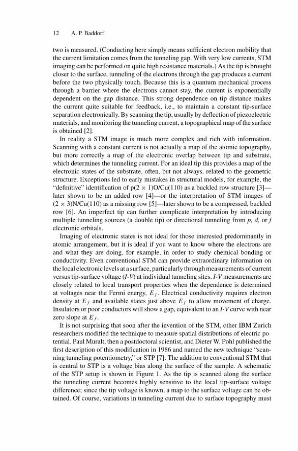
It is not surprising that soon after the invention of the STM, other IBM Zurichresearchers modified the technique to measure spatial distributions of electric po-tential. Paul Muralt, then a postdoctoral scientist, and Dieter W. Pohl published thefirst description of this modification in 1986 and named the new technique “scan-ning tunneling potentiometry,” or STP [7]. The addition to conventional STM thatis central to STP is a voltage bias along the surface of the sample. A schematicof the STP setup is shown in Figure 1. As the tip is scanned along the surfacethe tunneling current becomes highly sensitive to the local tip-surface voltagedifference; since the tip voltage is known, a map to the surface voltage can be ob-tained. Of course, variations in tunneling current due to surface topography must

I.1. Scanning Tunneling Potentiometry 13
FIGURE 1. Schematic illustration of the STP technique, which combines a lateral voltageacross the sample with an STM for imaging of the local surface topography and potential.
be distinguished from those due to the lateral voltage drop. Approaches to makethis distinction will be discussed below.
2 STP Technique
2.1 Sample Conditions
For conventional detection electronics and tunneling equipment, voltages must belimited to the order of tens of volts to avoid arcing and to protect sensitive amplifiers.Across a typical 1-cm sample, 10 V corresponds to 1 mV/µm or 1 µV/nm. Witha typical G� tunneling resistance, a uniform conductor would require equipmentwith a sensitivity of 1 pA/µm or 1 fA/nm. A femtoamp precision is too demandingfor common STP circuitry, but a pA is certainly achievable. One solution that canprovide a greater lateral resolution is to study smaller samples, for example, tolithographically create electrodes to apply the lateral voltage across a few tens ofmicrons. Another solution is to study materials that are not uniform, so that muchlarger voltage drops and corresponding tunneling current contrasts are observedat boundaries or defects of interest. However, sensitivity to small current changescan still be a limiting factor in STP spatial resolution.
For good conductors, even 10 V/cm is too large to maintain. A 1-cm-long coppersample with 1-mm-diameter cross section will draw a little over a 1,000 A withapplication of 10 V, and sample heating could be a problem! This illustration revealsthe need for relatively high resistance samples in STP to maintain a sufficientvoltage drop across the sample. To minimize current and sample heating, sampleresistances should be well over 100�. At the same time, STP’s foundation ontunneling current requires a non-insulating sample, with resistivity well beneath atypical tunneling resistance of a G�. Appropriate samples include semiconductors,poor metals, thin films, and nanometer structures. By reducing the dimensionsof the conductor, quite high current densities become possible. For example in