Embed Size (px)
Citation preview

REG102
SBVS024F – NOVEMBER 2000 – REVISED SEPTEMBER 2005
www.ti.com
PRODUCTION DATA information is current as of publication date.Products conform to specifications per the terms of Texas Instrumentsstandard warranty. Production processing does not necessarily includetesting of all parameters.
Copyright © 2000-2005, Texas Instruments Incorporated
DMOS250mA Low-Dropout Regulator
Please be aware that an important notice concerning availability, standard warranty, and use in critical applications ofTexas Instruments semiconductor products and disclaimers thereto appears at the end of this data sheet.
FEATURES NEW DMOS TOPOLOGY:
Ultra Low Dropout Voltage:150mV typ at 250mAOutput Capacitor not Required for Stability
FAST TRANSIENT RESPONSE
VERY LOW NOISE: 28µVrms
HIGH ACCURACY: ±1.5% max
HIGH EFFICIENCY:IGND = 600µA at IOUT = 250mANot Enabled: IGND = 0.01µA
2.5V, 2.8V, 2.85V, 3.0V, 3.3V, AND 5.0VADJUSTABLE OUTPUT VERSIONS
OTHER OUTPUT VOLTAGES AVAILABLE UPONREQUEST
FOLDBACK CURRENT LIMIT
THERMAL PROTECTION
SMALL SURFACE-MOUNT PACKAGES:SOT23-5, SOT223-5, and SO-8
APPLICATIONS PORTABLE COMMUNICATION DEVICES BATTERY-POWERED EQUIPMENT PERSONAL DIGITAL ASSISTANTS MODEMS BAR-CODE SCANNERS BACKUP POWER SUPPLIES
DESCRIPTIONThe REG102 is a family of low-noise, low-dropout linearregulators with low ground pin current. The new DMOStopology provides significant improvement over previousdesigns, including low-dropout voltage (only 150mV typ atfull load), and better transient performance. In addition, nooutput capacitor is required for stability, unlike conventionallow-dropout regulators that are difficult to compensate andrequire expensive low ESR capacitors greater than 1µF.
Typical ground pin current is only 600µA (at IOUT = 250mA)and drops to 10nA when not enabled. Unlike regulators withPNP pass devices, quiescent current remains relatively con-stant over load variations and under dropout conditions.
The REG102 has very low output noise (typically 28µVrmsfor VOUT = 3.3V with CNR = 0.01µF), making it ideal for usein portable communications equipment. On-chip trimmingresults in high output voltage accuracy. Accuracy is main-tained over temperature, line, and load variations. Key pa-rameters are tested over the specified temperature range(–40°C to +85°C).
The REG102 is well protected—internal circuitry provides acurrent limit that protects the load from damage; furthermore,thermal protection circuitry keeps the chip from being dam-aged by excessive temperature. The REG102 is available inSOT23-5, SOT223-5, and SO-8 packages.
REG102(Fixed Voltage
Versions)
Enable
GND
0.1µF COUT(1)
++VOUTVIN
NR
NR = Noise Reduction NOTE: (1) Optional.
REG102-A
GND
Enable
0.1µF+
COUT(1)
+
VOUTVIN
R2
R1
Adj
REG102 REG102
All trademarks are the property of their respective owners.

REG1022SBVS024Fwww.ti.com
PIN CONFIGURATIONS
Top View
VOUT(2)
VOUT(2)
NR/Adjust(1)
GND
VIN(3)
VIN(3)
NC
Enable
SO-8
1
2
3
4
8
7
6
5
NOTES: (1) For REG102A-A: voltage setting resistor pin.All other models: noise reduction capacitor pin.(2) Both pin 1 and pin 2 must be connected.(3) Both pin 7 and pin 8 must be connected.
SOT223-5
(U Package)
VIN
GND
Enable
VOUT
NR/Adjust(1)
SOT23-5
1
2
3
5
4
(N Package)
(G Package)
Tab is GND
EnableNR/Adjust(1)
GNDVIN
1 2 3 4 5
VOUT
ABSOLUTE MAXIMUM RATINGS(1)
Supply Input Voltage, VIN ....................................................... –0.3V to 12VEnable Input Voltage, VEN ....................................................... –0.3V to VIN
Feedback Voltage, VFB ........................................................ –0.3V to 6.0VNR Pin Voltage, VNR ............................................................. –0.3V to 6.0VOutput Short-Circuit Duration ...................................................... IndefiniteOperating Temperature Range (TJ) ................................ –55°C to +125°CStorage Temperature Range (TA) ................................... –65°C to +150°CLead Temperature (soldering, 3s) .................................................. +240°C
NOTE: (1) Stresses above these ratings may cause permanent damage.Exposure to absolute maximum conditions for extended periods may degradedevice reliability.
ELECTROSTATICDISCHARGE SENSITIVITY
This integrated circuit can be damaged by ESD. TexasInstruments recommends that all integrated circuits be handledwith appropriate precautions. Failure to observe proper han-dling and installation procedures can cause damage.
ESD damage can range from subtle performance degrada-tion to complete device failure. Precision integrated circuitsmay be more susceptible to damage because very smallparametric changes could cause the device not to meet itspublished specifications.
PACKAGE/ORDERING INFORMATION(1)
PRODUCT VOUT(2)
REG102xx-yyyy/zzz XX is package designator.
YYYY is typical output voltage (5 = 5.0V, 2.85 = 2.85V, A = Adjustable).
ZZZ is package quantity.
(1) For the most current package and ordering information, see the Package Option Addendum at the end of this document, or see the TI website at www.ti.com.
(2) Output voltages from 2.5V to 5.1V in 50mV increments are available; minimum order quantities apply. Contact factory for details and availability.

REG102 3SBVS024F www.ti.com
ELECTRICAL CHARACTERISTICSBoldface limits apply over the specified temperature range, TJ = –40°C to +85°C.At TJ = +25°C, VIN = VOUT + 1V (VOUT = 2.5V for REG102-A), VENABLE = 1.8V, IOUT = 5mA, CNR = 0.01µF, and COUT = 0.1µF(1), unless otherwise noted.
REG102NAREG102GAREG102UA
PARAMETER CONDITION MIN TYP MAX UNITS
OUTPUT VOLTAGEOutput Voltage Range VOUT
REG102-2.5 2.5 VREG102-2.8 2.8 VREG102-2.85 2.85 VREG102-3.0 3.0 VREG102-3.3 3.3 VREG102-5 5 VREG102-A 2.5 5.5 V
Reference Voltage VREF 1.26 VAdjust Pin Current IADJ 0.2 1 µA
Accuracy ±0.5 ±1.5 %Over Temperature ±2.3 %vs Temperature dVOUT/dT 50 ppm/°Cvs Line and Load IOUT = 5mA to 250mA, VIN = (VOUT + 0.4V) to 10V ±0.8 ±2.0 %Over Temperature VIN = (VOUT + 0.6V) to 10V ±2.8 %
DC DROPOUT VOLTAGE(2) VDROP IOUT = 5mA 4 10 mVFor all models IOUT = 250mA 150 220 mV
Over Temperature IOUT = 250mA 270 mV
VOLTAGE NOISEf = 10Hz to 100kHz VnWithout CNR (all models) CNR = 0, COUT = 0 23µVrms/V • VOUT µVrmsWith CNR (all fixed voltage models) CNR = 0.01µF, COUT = 10µF 7µVrms/V • VOUT µVrms
OUTPUT CURRENTCurrent Limit(3) ICL 340 400 470 mA
Over Temperature 300 490 mAShort-Circuit Current Limit ISC 150 mA
RIPPLE REJECTIONf = 120Hz 65 dB
ENABLE CONTROLVENABLE High (output enabled) VENABLE 1.8 VIN VVENABLE Low (output disabled) –0.2 0.5 VIENABLE High (output enabled) IENABLE VENABLE = 1.8V to VIN, VIN = 1.8V to 6.5(4) 1 100 nAIENABLE Low (output disabled) VENABLE = 0V to 0.5V 2 100 nAOutput Disable Time COUT = 1.0µF, RLOAD = 13Ω 50 µsOutput Enable Softstart Time COUT = 1.0µF, RLOAD = 13Ω 1.5 ms
THERMAL SHUTDOWNJunction Temperature
Shutdown 160 °CReset from Shutdown 140 °C
GROUND PIN CURRENTGround Pin Current IGND IOUT = 5mA 400 500 µA
IOUT = 250mA 600 800 µAEnable Pin Low VENABLE ≤ 0.5V 0.01 0.2 µA
INPUT VOLTAGE VINOperating Input Voltage Range(5) 1.8 10 VSpecified Input Voltage Range VIN > 1.8V VOUT + 0.4 10 V
Over Temperature VIN > 1.8V VOUT + 0.6 10 V
TEMPERATURE RANGESpecified Range TJ –40 +85 °COperating Range TJ –55 +125 °CStorage Range TA –65 +150 °CThermal Resistance
SOT23-5 Surface-Mount θJA Junction-to-Ambient 200 °C/WSO-8 Surface-Mount θJA Junction-to-Ambient 150 °C/WSOT223-5 Surface-Mount θJC Junction-to-Case 15 °C/W
θJA Junction-to-Ambient See Figure 8 °C/W
NOTES: (1) The REG102 does not require a minimum output capacitor for stability, however, transient response can be improved with proper capacitor selection.(2) Dropout voltage is defined as the input voltage minus the output voltage that produces a 2% change in the output voltage from the value at VIN = VOUT
+ 1V at fixed load.
(3) Current limit is the output current that produces a 10% change in output voltage from VIN = VOUT + 1V and IOUT = 5mA.(4) For VENABLE > 6.5V, see typical characteristic IENABLE vs VENABLE.(5) The REG102 no longer regulates when VIN < VOUT + VDROP (MAX). In dropout, the impedance from VIN to VOUT is typically less than 1Ω at TJ = +25°C.

REG1024SBVS024Fwww.ti.com
TYPICAL CHARACTERISTICSFor all models, at TJ = +25°C and VENABLE = 1.8V, unless otherwise noted.
500 10025 75 150125 175 200 225 250
0.80
0.60
0.40
0.20
0
–0.20
–0.40
–0.60
–0.80
Out
put V
olta
ge C
hang
e (%
)
IOUT (mA)
OUTPUT VOLTAGE CHANGE vs IOUT(VIN = VOUT + 1V, Output Voltage % Change
Referred to IOUT = 125mA at +25°C)
–55°C
+125°C
+25°C
–25–50 0 7525 50 100 125
0
–0.1
–0.2
–0.3
–0.4
–0.5
–0.6
–0.7
Out
put V
olta
ge C
hang
e (%
)
Temperature (°C)
LOAD REGULATION vs TEMPERATURE(VIN = VOUT + 1V)
5mA < IOUT < 250mA
25mA < IOUT < 250mA
0 1 2 3 4 5 86 7
20
15
10
5
0
–5
–10
–15
–20
Out
put V
olta
ge C
hang
e (m
V)
VIN – VOUT (V)
LINE REGULATION(Referred to VIN = VOUT + 1V at IOUT = 125mA)
IOUT = 5mA
All Fixed OutputVoltage Versions
IOUT = 125mA
IOUT = 250mA
–50 –25 0 25 50 75 100 125
0
–0.05
–0.10
–0.15
–0.20
–0.25
–0.30
Out
put V
olta
ge C
hang
e (%
)
Temperature (°C)
LINE REGULATION vs TEMPERATURE
IOUT = 250mA
(VOUT + 1V) < VIN < 10V
(VOUT + 0.4V) < VIN < 10V
0 50 150100 200 250
+125°C
250
200
150
100
50
0
DC
Dro
pout
Vol
tage
(m
V)
IOUT (mA)
DC DROPOUT VOLTAGE vs IOUT
+25°C
–55°C
–50 1251007550250–25
250
200
150
100
50
0
DC
Dro
pout
Vol
tage
(m
V)
Temperature (°C)
DC DROPOUT VOLTAGE vs TEMPERATURE
IOUT = 250mA

REG102 5SBVS024F www.ti.com
TYPICAL CHARACTERISTICS (Cont.)For all models, at TJ = +25°C and VENABLE = 1.8V, unless otherwise noted.
–1.0
–0.8
–0.6
–0.4
–0.2 0.0
0.2
0.4
0.6
0.8
1.0
18
16
14
12
10
8
6
4
2
0
Per
cent
age
of U
nits
(%
)
Error (%)
OUTPUT VOLTAGE ACCURACY HISTOGRAM
0 10 20 30 40 50 60 70 80 90 1005 15 25 35 45 55 65 75 85 95
30
25
20
15
10
5
0
Per
cent
age
of U
nits
(%
)
VOUT Drift (ppm/°C)
OUTPUT VOLTAGE DRIFT HISTOGRAM
–50 25–25 0 50 75 100 125
0.80
0.60
0.40
0.20
0
–0.20
–0.40
–0.60
–0.80
–1.00
Out
put V
olta
ge C
hang
e (%
)
Temperature (°C)
OUTPUT VOLTAGE vs TEMPERATURE(Output Voltage % Change Refered
to IOUT = 125mA at +25°C)
IOUT = 5mA
IOUT = 250mA
IOUT = 125mA
–50 25–25 0 50 75 100 125
1µ
100n
10n
1n
100p
I GN
D (
A)
Temperature (°C)
GROUND PIN CURRENT, NOT ENABLEDvs TEMPERATURE
VENABLE = 0.5VVIN = VOUT + 1V
0 50 7525 125100 175150 225200 250
800
700
600
500
400
300
200
100
0
I GN
D (
µA)
IOUT (mA)
GROUND PIN CURRENT vs IOUT
VOUT = 2.5V
VOUT = 3.3V
VOUT = 5.0V
–50 –25 0 25 50 75 125100
750
725
700
675
650
625
600
575
550
I GN
D (
µA)
Temperature (°C)
GROUND PIN CURRENT vs TEMPERATURE
IOUT = 250mAVOUT = 5V
VOUT = 3.3V
VOUT = 2.5V
REG1026SBVS024Fwww.ti.com
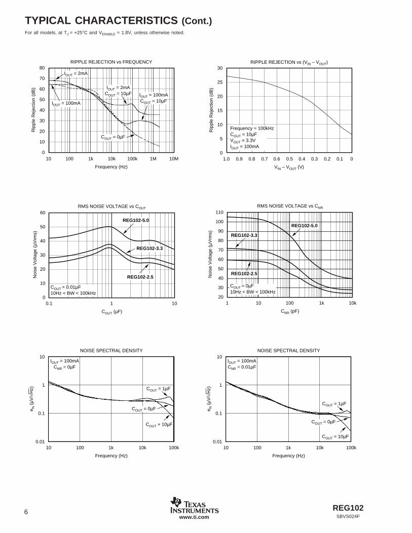
TYPICAL CHARACTERISTICS (Cont.)For all models, at TJ = +25°C and VENABLE = 1.8V, unless otherwise noted.
10 100 1k 10k 100k 10M1M
80
70
60
50
40
30
20
10
0
Rip
ple
Rej
ectio
n (d
B)
Frequency (Hz)
RIPPLE REJECTION vs FREQUENCY
IOUT = 2mA
IOUT = 100mA
IOUT = 2mACOUT = 10µF IOUT = 100mA
COUT = 10µF
COUT = 0µF
1.0 0.9 0.60.8 0.7 0.5 0.4 0.3 00.2 0.1
30
25
20
15
10
5
0
Rip
ple
Rej
ectio
n (d
B)
VIN – VOUT (V)
RIPPLE REJECTION vs (VIN – VOUT)
Frequency = 100kHzCOUT = 10µFVOUT = 3.3VIOUT = 100mA
1 100 1k10
REG102-5.0
REG102-3.3
REG102-2.5
10k
110
100
90
80
70
60
50
40
30
20
Noi
se V
olta
ge (
µVrm
s)
CNR (pF)
RMS NOISE VOLTAGE vs CNR
COUT = 0µF10Hz < BW < 100kHz
10 100 1k 10k 100k
10
1
0.1
0.01
e N (
µV/√
Hz)
Frequency (Hz)
NOISE SPECTRAL DENSITY
IOUT = 100mACNR = 0µF
COUT = 1µF
COUT = 0µF
COUT = 10µF
10 100 1k 10k 100k
10
1
0.1
0.01
e N (
µV/√
Hz)
Frequency (Hz)
NOISE SPECTRAL DENSITY
IOUT = 100mACNR = 0.01µF
COUT = 1µF
COUT = 0µF
COUT = 10µF
0.1 1 10
60
50
40
30
20
10
0
Noi
se V
olta
ge (
µVrm
s)
COUT (µF)
RMS NOISE VOLTAGE vs COUT
REG102-5.0
REG102-3.3
REG102-2.5
COUT = 0.01µF10Hz < BW < 100kHz
REG102 7SBVS024F www.ti.com
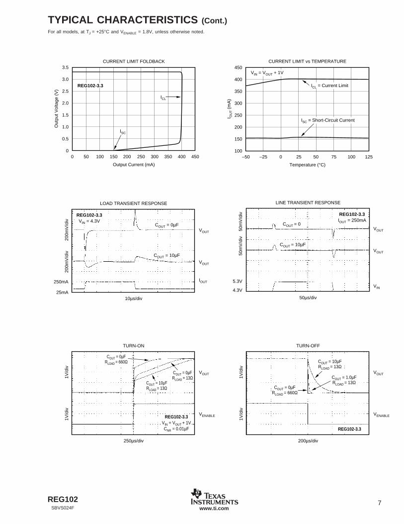
TYPICAL CHARACTERISTICS (Cont.)For all models, at TJ = +25°C and VENABLE = 1.8V, unless otherwise noted.
0 50 100 150 200 250 300 350
ISC
ICL
400 450
3.5
3.0
2.5
2.0
1.5
1.0
0.5
0
Out
put V
olta
ge (
V)
Output Current (mA)
CURRENT LIMIT FOLDBACK
REG102-3.3
–50 –25 0 25 50 75 125100
450
400
350
300
250
200
150
100
I OU
T (
mA
)
Temperature (°C)
CURRENT LIMIT vs TEMPERATURE
VIN = VOUT + 1V
ICL = Current Limit
ISC = Short-Circuit Current
LOAD TRANSIENT RESPONSE
10µs/div
REG102-3.3VIN = 4.3V
250mA
200m
V/d
iv20
0mV
/div
IOUT
VOUT
VOUT
25mA
COUT = 0µF
COUT = 10µF
LINE TRANSIENT RESPONSE
50µs/div
5.3V
50m
V/d
iv50
mV
/div
VIN
VOUT
VOUT
4.3V
REG102-3.3IOUT = 250mA
COUT = 0
COUT = 10µF
TURN-ON
250µs/div
1V/d
iv1V
/div
VENABLE
VOUT
REG102-3.3VIN = VOUT + 1VCNR = 0.01µF
COUT = 10µFRLOAD = 13Ω
COUT = 0µFRLOAD = 13Ω
COUT = 0µFRLOAD = 660Ω
TURN-OFF
200µs/div
1V/d
iv1V
/div
VENABLE
VOUT
REG102-3.3
COUT = 10µFRLOAD = 13Ω
COUT = 1.0µFRLOAD = 13Ω
COUT = 0µFRLOAD = 660Ω

REG1028SBVS024Fwww.ti.com
TYPICAL CHARACTERISTICS (Cont.)For all models, at TJ = +25°C and VENABLE = 1.8V, unless otherwise noted.
6 7 8 9 10
10µ
1.0µ
100n
10n
1n
I EN
AB
LE (
A)
VENABLE (V)
IENABLE vs VENABLE
T = +25°C
T = –55°C
T = +125°C
POWER UP/POWER DOWN
1s/div
500m
V/d
iv
VOUT = 3.0VRLOAD = 12Ω
10 100 1k 10k 100k
80
70
60
50
40
30
20
VN (
rms)
CADJ (pF)
RMS NOISE VOLTAGE vs CADJ
VOUT = 3.3V
COUT = 0.1µF10Hz < frequency < 100kHz
–50 –25 0 25 50 75 100 125
0.350
0.300
0.250
0.200
0.150
0.100
0.050
0
I AD
J (µ
A)
Temperature (°C)
ADJUST PIN CURRENT vs TEMPERATURE
200mV/div
200mV/div
25mA
VOUT
COUT = 0
REG102–A
VIN = 4.3V
VOUT = 3.3V
COUT = 10µFVOUT
IOUT
250mA
LOAD TRANSIENT-ADJUSTABLE VERSION
50mV/div
50mV/div
4.3V
VOUTCOUT = 0
REG102–AIOUT = 250mACFB = 0.01µFVOUT = 3.3V
COUT = 10µFVOUT
VIN5.3V
LINE TRANSIENT-ADJUSTABLE VERSION

REG102 9SBVS024F www.ti.com
FIGURE 1. Fixed Voltage Nominal Circuit for the REG102.
REG102
Enable
VOUT
COUT
VIN
0.1µF
CNR0.01µF
GND NR
In Out
Optional
FIGURE 2. Adjustable Voltage Circuit for the REG102A.
FIGURE 3. Foldback Current Limit of the REG102-3.3 at 25°C.
VOUT = (1 + R1/R2) • 1.26V
Pin numbers for the SOT-223 package.
REG102VIN
0.1µF
3
1
Gnd
VOUT
R1CFB0.01µF
COUT
Adj
R2
IADJ
Load
2
4
5
Enable
To reduce current through divider, increase resistor values (see table at right).As the impedance of the resistor divider increases, IADJ (~200nA) may introduce an error.CFB improves noise and transient response.
VOUT (V) R1 (Ω)(1) R2 (Ω)(1)
2.5 11.3k 11.5k1.13k 1.15k
3.0 15.8k 11.5k1.58k 1.15k
3.3 18.7k 11.5k1.87k 1.15k
5.0 34.0k 11.5k3.40k 1.15k
NOTE: (1) Resistors are standard 1% values.
EXAMPLE RESISTOR VALUES
Optional
0 50 100 150 200 250 300 350
ISC
ICL
400 450
3.5
3
2.5
2
1.5
1
0.5
0
Out
put V
olta
ge (
V)
Output Current (mA)
CURRENT LIMIT FOLDBACK
REG102-3.3
BASIC OPERATIONThe REG102 series of LDO (low dropout) linear regulatorsoffers a wide selection of fixed output voltage versions andan adjustable output version as well. The REG102 belongsto a family of new generation LDO regulators that use aDMOS pass transistor to achieve ultra low-dropout perfor-mance and freedom from output capacitor constraints. Groundpin current remains under 1mA over all line, load, andtemperature conditions. All versions have thermal and over-current protection, including foldback current limit.
The REG102 does not require an output capacitor for regulatorstability and is stable over most output currents and with almostany value and type of output capacitor up to 10µF or more. Forapplications where the regulator output current drops belowseveral milliamps, stability can be enhanced by adding a 1kΩto 2kΩ load resistor, using capacitance values smaller than10µF, or keeping the effective series resistance greater than0.05Ω including the capacitor ESR and parasitic resistance inprinted circuit board traces, solder joints, and sockets.
Although an input capacitor is not required, it is a goodstandard analog design practice to connect a 0.1µF low ESRcapacitor across the input supply voltage. This is recom-mended to counteract reactive input sources and improveripple rejection by reducing input voltage ripple.
Figure 1 shows the basic circuit connections for the fixedvoltage models. Figure 2 gives the connections for the adjust-able output version (REG102A) and example resistor values forsome commonly used output voltages. Values for other volt-ages can be calculated from the equation shown in Figure 2.
INTERNAL CURRENT LIMIT
The REG102 internal current limit has a typical value of400mA. A foldback feature limits the short-circuit current to atypical short-circuit value of 150mA, which helps to protect
the regulator from damage under all load conditions. Acharacteristic of VOUT versus IOUT is given in Figure 3 and inthe Typical Characteristics section.

REG10210SBVS024Fwww.ti.com
FIGURE 4. Block Diagram.
FIGURE 5. Output Noise versus Noise Reduction Capacitor.
0.1 100 1k10 10k
110
100
90
80
70
60
50
40
30
20
Noi
se V
olta
ge (
Vrm
s)
CNR (pF)
RMS NOISE VOLTAGE vs CNR
REG102-5.0
REG102-3.3
REG102-2.5
COUT = 0µF10Hz < BW < 100kHz
Over-CurrentOver TempProtection
VREF(1.26V)
Low-NoiseCharge Pump
DMOSOutput
R1
NOTE: R1 and R2 are internalon fixed output versions.
VOUT
Adj(adjustableversions)R2
NR(fixed output
versions only)
Enable
REG102
VIN
CNR(optional)
ENABLE
The Enable pin is active high and compatible with standardTTL-CMOS levels. Inputs below 0.5V (max) turn the regula-tor off and all circuitry is disabled. Under this condition,ground pin current drops to approximately 10nA. When notused, the Enable pin can be connected to VIN. When a pull-up resistor is used, and operation below 1.8V is required, usepull-up resistor values below 50kΩ.
OUTPUT NOISE
A precision bandgap reference is used to generate theinternal reference voltage, VREF. This reference is the domi-nant noise source within the REG102 and generates approxi-mately 29µVrms in the 10Hz to 100kHz bandwidth at thereference output. The regulator control loop gains up thereference noise, so that the noise voltage of the regulator isapproximately given by:
V VrmsR R
RVrms
VVN
OUT
REF= µ + = µ •29
2291 2
(1)
As the value of VREF is 1.26V, this relationship reduces to:
VVrmsV
VN OUT= µ •23 (2)
Connecting a capacitor, CNR, from the Noise Reduction (NR)pin to ground forms a low-pass filter for the voltage refer-ence. Adding CNR (as shown in Figure 4) forms a low-passfilter for the voltage reference. For CNR = 10nF, the total noisein the 10Hz to 100kHz bandwidth is reduced by approxi-mately a factor of 2.8 for VOUT = 3.3V. This noise reductioneffect is shown in Figure 5 and as RMS Noise Voltage vs CNR
in the Typical Characteristics section.
Noise can be further reduced by carefully choosing an outputcapacitor, COUT. Best overall noise performance is achievedwith very low (< 0.22µF) or very high (> 2.2µF) values of COUT
(see the RMS Noise Voltage vs COUT typical characteristic).
The REG102 uses an internal charge pump to develop aninternal supply voltage sufficient to drive the gate of theDMOS pass element above VIN. The charge-pump switchingnoise (nominal switching frequency = 2MHz) is not measur-able at the output of the regulator over most values of IOUT
and COUT.
The REG102 adjustable version does not have the noise-reduction pin available; however, the adjust pin is the sum-ming junction of the error amplifier. A capacitor, CFB, con-nected from the output to the adjust pin can reduce both theoutput noise and the peak error from a load transient (see thetypical characteristics for output noise performance).

REG102 11SBVS024F www.ti.com
FIGURE 6. Transient and DC Dropout.
350
300
250
200
150
100
50
0
Dro
pout
Vol
tage
(m
V)
0 50 100 150 200
DC
250
IOUT (mA)
DROPOUT VOLTAGE vs IOUT
0mA to IOUT Transient
DROPOUT VOLTAGE
The REG102 uses an N-channel DMOS as the pass element.When (VIN – VOUT) is less than the drop-out voltage (VDROP),the DMOS pass device behaves like a resistor; therefore, forlow values of (VIN – VOUT), the regulator input-to-outputresistance is the RdsON of the DMOS pass element (typically600mΩ). For static (DC) loads, the REG102 typically main-tains regulation down to a (VIN – VOUT) voltage drop of 150mVat full rated output current. In Figure 6, the bottom line (DCdropout) shows the minimum VIN to VOUT voltage drop re-quired to prevent dropout under DC load conditions.
For large step changes in load current, the REG102 requiresa larger voltage drop across it to avoid degraded transientresponse. The boundary of this transient drop-out region isshown as the top line in Figure 6 and values of VIN to VOUT
voltage drop above this line insure normal transient re-sponse.
case conditions (full-scale load change with (VIN – VOUT)voltage drop close to DC dropout levels), the REG102 cantake several hundred microseconds to re-enter the specifiedwindow of regulation.
TRANSIENT RESPONSE
The REG102 response to transient line and load conditionsimproves at lower output voltages. The addition of a capacitor(nominal value 0.47µF) from the output pin to ground canimprove the transient response. In the adjustable version, theaddition of a capacitor, CFB (nominal value 10nF), from theoutput to the adjust pin can also improve the transientresponse.
THERMAL PROTECTION
Power dissipated within the REG102 can cause the junctiontemperature to rise. The REG102 has thermal shutdowncircuitry that protects the regulator from damage which dis-ables the output when the junction temperature reachesapproximately 160°C, allowing the device to cool. When thejunction temperature cools to approximately 140°C, the out-put circuitry is again enabled. Depending on various condi-tions, the thermal protection circuit can cycle on and off. Thislimits the dissipation of the regulator, but can have anundesirable effect on the load.
Any tendency to activate the thermal protection circuit indi-cates excessive power dissipation or an inadequate heatsink. For reliable operation, junction temperature must belimited to 125°C, maximum. To estimate the margin of safetyin a complete design (including heat sink), increase theambient temperature until the thermal protection is triggered;use worst-case loads and signal conditions. For good reliabil-ity, thermal protection should trigger more than 35°C abovethe maximum expected ambient condition of the application.This produces a worst-case junction temperature of 125°C atthe highest expected ambient temperature and worst-caseload.
The internal protection circuitry of the REG102 is designed toprotect against overload conditions and is not intended toreplace proper heat sinking. Continuously running the REG102into thermal shutdown will degrade reliability.
In the transient dropout region between DC and Transient,transient response recovery time increases. The time requiredto recover from a load transient is a function of both themagnitude and rate of the step change in load current and theavailable headroom VIN to VOUT voltage drop. Under worst-

REG10212SBVS024Fwww.ti.com
FIGURE 7. Maximum Power Dissipation versus Ambient Temperature for the Various Packages and PCB Heat Sink Configurations.
FIGURE 8. Thermal Resistance versus PCB Area for the Five-Lead SOT-223.
THERMAL RESISTANCE vs PCB COPPER AREA180
160
140
120
100
80
60
40
20
0
The
rmal
Res
ista
nce,
JA
(°C
/W)
θ
0 1 2 3 4 5
Copper Area (inches2)
Circuit-Board Copper Area
REG102SOT-223 Surface-Mount Package
REG102Surface-Mount Package
1 oz. copper
2.5
2
1.5
1
0.5
0
Pow
er D
issi
patio
n (W
atts
)
0 25 50 75 125100
Ambient Temperature (°C)
DEVICE DISSIPATION vs TEMPERATURE
CONDITION PACKAGE PCB AREAJA
1 SOT-223 4in2 Top Side Only 53°C/W2 SOT-223 0.5in2 Top Side Only 110°C/W3 SO-8 — 150°C/W4 SOT-23 — 200°C/W
CONDITIONS#1#2#3#4
θ
POWER DISSIPATION
The REG102 is available in three different package configu-rations. The ability to remove heat from the die is different foreach package type and, therefore, presents different consid-erations in the printed circuit board (PCB) layout. The PCBarea around the device that is free of other componentsmoves the heat from the device to the ambient air. Althoughit is difficult to impossible to quantify all of the variables in athermal design of this type, performance data for severalsimplified configurations are shown in Figure 7. In all cases,the PCB copper area is bare copper (free of solder resistmask), not solder plated, and are for 1-ounce copper. Usingheavier copper will increase the effectiveness in moving theheat from the device. In those examples where there iscopper on both sides of the PCB, no connection has beenprovided between the two sides. The addition of platedthrough holes will improve the heat sink effectiveness.
Power dissipation depends on input voltage, load conditions,and duty cycle and is equal to the product of the averageoutput current times the voltage across the output element,VIN to VOUT voltage drop.
P V V ID IN OUT OUT= •( – ) (3)
Power dissipation can be minimized by using the lowestpossible input voltage necessary to assure the requiredoutput voltage.
REGULATOR MOUNTING
The tab of the SOT-223 package is electrically connected toground. For best thermal performance, this tab must besoldered directly to a circuit-board copper area. Increasingthe copper area improves heat dissipation, as shown inFigure 8.
Although the tab of the SOT-223 is electrical ground, it is notintended to carry current. The copper pad that acts as a heatsink should be isolated from the rest of the circuit to preventcurrent flow through the device from the tab to the groundpin. Solder pad footprint recommendations for the variousREG102 devices are presented in Application Bulletin SolderPad Recommendations for Surface-Mount Devices(SBFA015), available from the Texas Instruments web site(www.ti.com).

PACKAGE OPTION ADDENDUM
www.ti.com 24-Aug-2018
Addendum-Page 1
PACKAGING INFORMATION
Orderable Device Status(1)
Package Type PackageDrawing
Pins PackageQty
Eco Plan(2)
Lead/Ball Finish(6)
MSL Peak Temp(3)
Op Temp (°C) Device Marking(4/5)
Samples
REG102GA-2.5 ACTIVE SOT-223 DCQ 6 78 Green (RoHS& no Sb/Br)
CU NIPDAU Level-2-260C-1 YEAR R102G25
REG102GA-2.85 ACTIVE SOT-223 DCQ 6 78 Green (RoHS& no Sb/Br)
CU NIPDAU Level-2-260C-1 YEAR R102285
REG102GA-2.85G4 ACTIVE SOT-223 DCQ 6 78 Green (RoHS& no Sb/Br)
CU NIPDAU Level-2-260C-1 YEAR R102285
REG102GA-3 ACTIVE SOT-223 DCQ 6 78 Green (RoHS& no Sb/Br)
CU NIPDAU Level-2-260C-1 YEAR -40 to 85 R102G30
REG102GA-3.3 ACTIVE SOT-223 DCQ 6 78 Green (RoHS& no Sb/Br)
CU NIPDAU Level-2-260C-1 YEAR -40 to 85 R102G33
REG102GA-3.3/2K5 ACTIVE SOT-223 DCQ 6 2500 Green (RoHS& no Sb/Br)
CU NIPDAU Level-2-260C-1 YEAR -40 to 85 R102G33
REG102GA-3.3G4 ACTIVE SOT-223 DCQ 6 78 Green (RoHS& no Sb/Br)
CU NIPDAU Level-2-260C-1 YEAR -40 to 85 R102G33
REG102GA-3G4 ACTIVE SOT-223 DCQ 6 78 Green (RoHS& no Sb/Br)
CU NIPDAU Level-2-260C-1 YEAR -40 to 85 R102G30
REG102GA-5 ACTIVE SOT-223 DCQ 6 78 Green (RoHS& no Sb/Br)
CU NIPDAU Level-2-260C-1 YEAR -40 to 85 R102G50
REG102GA-A ACTIVE SOT-223 DCQ 6 78 Green (RoHS& no Sb/Br)
CU NIPDAU Level-2-260C-1 YEAR R102GA
REG102GA-A/2K5 ACTIVE SOT-223 DCQ 6 2500 Green (RoHS& no Sb/Br)
CU NIPDAU Level-2-260C-1 YEAR R102GA
REG102GA-A/2K5G4 ACTIVE SOT-223 DCQ 6 2500 Green (RoHS& no Sb/Br)
CU NIPDAU Level-2-260C-1 YEAR R102GA
REG102GA-AG4 ACTIVE SOT-223 DCQ 6 78 Green (RoHS& no Sb/Br)
CU NIPDAU Level-2-260C-1 YEAR R102GA
REG102NA-2.5/250 ACTIVE SOT-23 DBV 5 250 Green (RoHS& no Sb/Br)
CU NIPDAU Level-1-260C-UNLIM RO2D
REG102NA-2.5/250G4 ACTIVE SOT-23 DBV 5 250 Green (RoHS& no Sb/Br)
CU NIPDAU Level-1-260C-UNLIM RO2D
REG102NA-2.8/250 ACTIVE SOT-23 DBV 5 250 Green (RoHS& no Sb/Br)
CU NIPDAU Level-1-260C-UNLIM RO2E
REG102NA-2.85/250 ACTIVE SOT-23 DBV 5 250 Green (RoHS& no Sb/Br)
CU NIPDAU Level-1-260C-UNLIM RO2N

PACKAGE OPTION ADDENDUM
www.ti.com 24-Aug-2018
Addendum-Page 2
Orderable Device Status(1)
Package Type PackageDrawing
Pins PackageQty
Eco Plan(2)
Lead/Ball Finish(6)
MSL Peak Temp(3)
Op Temp (°C) Device Marking(4/5)
Samples
REG102NA-2.85/3K ACTIVE SOT-23 DBV 5 3000 Green (RoHS& no Sb/Br)
CU NIPDAU Level-1-260C-UNLIM RO2N
REG102NA-3.3/250 ACTIVE SOT-23 DBV 5 250 Green (RoHS& no Sb/Br)
CU NIPDAU Level-1-260C-UNLIM -40 to 85 RO2C
REG102NA-3.3/3K ACTIVE SOT-23 DBV 5 3000 Green (RoHS& no Sb/Br)
CU NIPDAU Level-1-260C-UNLIM -40 to 85 RO2C
REG102NA-3/250 ACTIVE SOT-23 DBV 5 250 Green (RoHS& no Sb/Br)
CU NIPDAU Level-1-260C-UNLIM -40 to 85 RO2G
REG102NA-3/250G4 ACTIVE SOT-23 DBV 5 250 Green (RoHS& no Sb/Br)
CU NIPDAU Level-1-260C-UNLIM -40 to 85 RO2G
REG102NA-3/3K ACTIVE SOT-23 DBV 5 3000 Green (RoHS& no Sb/Br)
CU NIPDAU Level-1-260C-UNLIM -40 to 85 RO2G
REG102NA-3/3KG4 ACTIVE SOT-23 DBV 5 3000 Green (RoHS& no Sb/Br)
CU NIPDAU Level-1-260C-UNLIM -40 to 85 RO2G
REG102NA-5/250 ACTIVE SOT-23 DBV 5 250 Green (RoHS& no Sb/Br)
CU NIPDAU Level-1-260C-UNLIM -40 to 85 RO2B
REG102NA-5/250G4 ACTIVE SOT-23 DBV 5 250 Green (RoHS& no Sb/Br)
CU NIPDAU Level-1-260C-UNLIM -40 to 85 RO2B
REG102NA-5/3K ACTIVE SOT-23 DBV 5 3000 Green (RoHS& no Sb/Br)
CU NIPDAU Level-1-260C-UNLIM -40 to 85 RO2B
REG102NA-5/3KG4 ACTIVE SOT-23 DBV 5 3000 Green (RoHS& no Sb/Br)
CU NIPDAU Level-1-260C-UNLIM -40 to 85 RO2B
REG102NA-A/250 ACTIVE SOT-23 DBV 5 250 Green (RoHS& no Sb/Br)
CU NIPDAU Level-1-260C-UNLIM RO2A
REG102NA-A/250G4 ACTIVE SOT-23 DBV 5 250 Green (RoHS& no Sb/Br)
CU NIPDAU Level-1-260C-UNLIM RO2A
REG102NA-A/3K ACTIVE SOT-23 DBV 5 3000 Green (RoHS& no Sb/Br)
CU NIPDAU Level-1-260C-UNLIM RO2A
REG102UA-2.5 ACTIVE SOIC D 8 75 Green (RoHS& no Sb/Br)
CU NIPDAU Level-2-260C-1 YEAR REG102U25
REG102UA-3 ACTIVE SOIC D 8 75 Green (RoHS& no Sb/Br)
CU NIPDAU Level-2-260C-1 YEAR -40 to 85 REG102U30
REG102UA-3.3 ACTIVE SOIC D 8 75 Green (RoHS& no Sb/Br)
CU NIPDAU Level-2-260C-1 YEAR -40 to 85 REG102U33
REG102UA-3.3/2K5 ACTIVE SOIC D 8 2500 Green (RoHS& no Sb/Br)
CU NIPDAU Level-2-260C-1 YEAR -40 to 85 REG102U33

PACKAGE OPTION ADDENDUM
www.ti.com 24-Aug-2018
Addendum-Page 3
Orderable Device Status(1)
Package Type PackageDrawing
Pins PackageQty
Eco Plan(2)
Lead/Ball Finish(6)
MSL Peak Temp(3)
Op Temp (°C) Device Marking(4/5)
Samples
REG102UA-3G4 ACTIVE SOIC D 8 75 Green (RoHS& no Sb/Br)
CU NIPDAU Level-2-260C-1 YEAR -40 to 85 REG102U30
REG102UA-5 ACTIVE SOIC D 8 75 Green (RoHS& no Sb/Br)
CU NIPDAU Level-2-260C-1 YEAR -40 to 85 REG102U50
REG102UA-5/2K5 ACTIVE SOIC D 8 2500 Green (RoHS& no Sb/Br)
CU NIPDAU Level-2-260C-1 YEAR -40 to 85 REG102U50
REG102UA-5G4 ACTIVE SOIC D 8 75 Green (RoHS& no Sb/Br)
CU NIPDAU Level-2-260C-1 YEAR -40 to 85 REG102U50
(1) The marketing status values are defined as follows:ACTIVE: Product device recommended for new designs.LIFEBUY: TI has announced that the device will be discontinued, and a lifetime-buy period is in effect.NRND: Not recommended for new designs. Device is in production to support existing customers, but TI does not recommend using this part in a new design.PREVIEW: Device has been announced but is not in production. Samples may or may not be available.OBSOLETE: TI has discontinued the production of the device.
(2) RoHS: TI defines "RoHS" to mean semiconductor products that are compliant with the current EU RoHS requirements for all 10 RoHS substances, including the requirement that RoHS substancedo not exceed 0.1% by weight in homogeneous materials. Where designed to be soldered at high temperatures, "RoHS" products are suitable for use in specified lead-free processes. TI mayreference these types of products as "Pb-Free".RoHS Exempt: TI defines "RoHS Exempt" to mean products that contain lead but are compliant with EU RoHS pursuant to a specific EU RoHS exemption.Green: TI defines "Green" to mean the content of Chlorine (Cl) and Bromine (Br) based flame retardants meet JS709B low halogen requirements of <=1000ppm threshold. Antimony trioxide basedflame retardants must also meet the <=1000ppm threshold requirement.
(3) MSL, Peak Temp. - The Moisture Sensitivity Level rating according to the JEDEC industry standard classifications, and peak solder temperature.
(4) There may be additional marking, which relates to the logo, the lot trace code information, or the environmental category on the device.
(5) Multiple Device Markings will be inside parentheses. Only one Device Marking contained in parentheses and separated by a "~" will appear on a device. If a line is indented then it is a continuationof the previous line and the two combined represent the entire Device Marking for that device.
(6) Lead/Ball Finish - Orderable Devices may have multiple material finish options. Finish options are separated by a vertical ruled line. Lead/Ball Finish values may wrap to two lines if the finishvalue exceeds the maximum column width.
Important Information and Disclaimer:The information provided on this page represents TI's knowledge and belief as of the date that it is provided. TI bases its knowledge and belief on informationprovided by third parties, and makes no representation or warranty as to the accuracy of such information. Efforts are underway to better integrate information from third parties. TI has taken andcontinues to take reasonable steps to provide representative and accurate information but may not have conducted destructive testing or chemical analysis on incoming materials and chemicals.TI and TI suppliers consider certain information to be proprietary, and thus CAS numbers and other limited information may not be available for release.

PACKAGE OPTION ADDENDUM
www.ti.com 24-Aug-2018
Addendum-Page 4
In no event shall TI's liability arising out of such information exceed the total purchase price of the TI part(s) at issue in this document sold by TI to Customer on an annual basis.
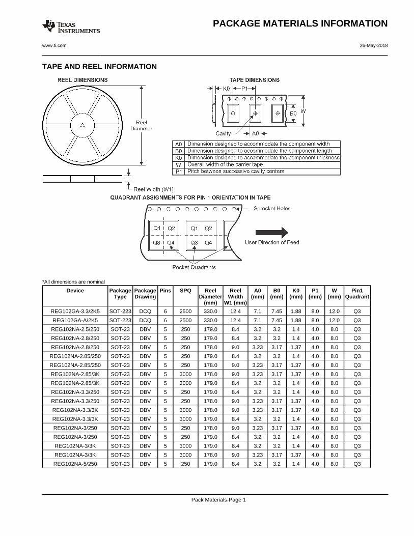
TAPE AND REEL INFORMATION
*All dimensions are nominal
Device PackageType
PackageDrawing
Pins SPQ ReelDiameter
(mm)
ReelWidth
W1 (mm)
A0(mm)
B0(mm)
K0(mm)
P1(mm)
W(mm)
Pin1Quadrant
REG102GA-3.3/2K5 SOT-223 DCQ 6 2500 330.0 12.4 7.1 7.45 1.88 8.0 12.0 Q3
REG102GA-A/2K5 SOT-223 DCQ 6 2500 330.0 12.4 7.1 7.45 1.88 8.0 12.0 Q3
REG102NA-2.5/250 SOT-23 DBV 5 250 179.0 8.4 3.2 3.2 1.4 4.0 8.0 Q3
REG102NA-2.8/250 SOT-23 DBV 5 250 179.0 8.4 3.2 3.2 1.4 4.0 8.0 Q3
REG102NA-2.8/250 SOT-23 DBV 5 250 178.0 9.0 3.23 3.17 1.37 4.0 8.0 Q3
REG102NA-2.85/250 SOT-23 DBV 5 250 179.0 8.4 3.2 3.2 1.4 4.0 8.0 Q3
REG102NA-2.85/250 SOT-23 DBV 5 250 178.0 9.0 3.23 3.17 1.37 4.0 8.0 Q3
REG102NA-2.85/3K SOT-23 DBV 5 3000 178.0 9.0 3.23 3.17 1.37 4.0 8.0 Q3
REG102NA-2.85/3K SOT-23 DBV 5 3000 179.0 8.4 3.2 3.2 1.4 4.0 8.0 Q3
REG102NA-3.3/250 SOT-23 DBV 5 250 179.0 8.4 3.2 3.2 1.4 4.0 8.0 Q3
REG102NA-3.3/250 SOT-23 DBV 5 250 178.0 9.0 3.23 3.17 1.37 4.0 8.0 Q3
REG102NA-3.3/3K SOT-23 DBV 5 3000 178.0 9.0 3.23 3.17 1.37 4.0 8.0 Q3
REG102NA-3.3/3K SOT-23 DBV 5 3000 179.0 8.4 3.2 3.2 1.4 4.0 8.0 Q3
REG102NA-3/250 SOT-23 DBV 5 250 178.0 9.0 3.23 3.17 1.37 4.0 8.0 Q3
REG102NA-3/250 SOT-23 DBV 5 250 179.0 8.4 3.2 3.2 1.4 4.0 8.0 Q3
REG102NA-3/3K SOT-23 DBV 5 3000 179.0 8.4 3.2 3.2 1.4 4.0 8.0 Q3
REG102NA-3/3K SOT-23 DBV 5 3000 178.0 9.0 3.23 3.17 1.37 4.0 8.0 Q3
REG102NA-5/250 SOT-23 DBV 5 250 179.0 8.4 3.2 3.2 1.4 4.0 8.0 Q3
PACKAGE MATERIALS INFORMATION
www.ti.com 26-May-2018
Pack Materials-Page 1

Device PackageType
PackageDrawing
Pins SPQ ReelDiameter
(mm)
ReelWidth
W1 (mm)
A0(mm)
B0(mm)
K0(mm)
P1(mm)
W(mm)
Pin1Quadrant
REG102NA-5/250 SOT-23 DBV 5 250 178.0 9.0 3.23 3.17 1.37 4.0 8.0 Q3
REG102NA-5/3K SOT-23 DBV 5 3000 178.0 9.0 3.23 3.17 1.37 4.0 8.0 Q3
REG102NA-5/3K SOT-23 DBV 5 3000 179.0 8.4 3.2 3.2 1.4 4.0 8.0 Q3
REG102NA-A/250 SOT-23 DBV 5 250 179.0 8.4 3.2 3.2 1.4 4.0 8.0 Q3
REG102NA-A/3K SOT-23 DBV 5 3000 179.0 8.4 3.2 3.2 1.4 4.0 8.0 Q3
REG102UA-3.3/2K5 SOIC D 8 2500 330.0 12.4 6.4 5.2 2.1 8.0 12.0 Q1
REG102UA-5/2K5 SOIC D 8 2500 330.0 12.4 6.4 5.2 2.1 8.0 12.0 Q1
*All dimensions are nominal
Device Package Type Package Drawing Pins SPQ Length (mm) Width (mm) Height (mm)
REG102GA-3.3/2K5 SOT-223 DCQ 6 2500 346.0 346.0 29.0
REG102GA-A/2K5 SOT-223 DCQ 6 2500 346.0 346.0 29.0
REG102NA-2.5/250 SOT-23 DBV 5 250 203.0 203.0 35.0
REG102NA-2.8/250 SOT-23 DBV 5 250 203.0 203.0 35.0
REG102NA-2.8/250 SOT-23 DBV 5 250 180.0 180.0 18.0
REG102NA-2.85/250 SOT-23 DBV 5 250 203.0 203.0 35.0
REG102NA-2.85/250 SOT-23 DBV 5 250 180.0 180.0 18.0
REG102NA-2.85/3K SOT-23 DBV 5 3000 180.0 180.0 18.0
REG102NA-2.85/3K SOT-23 DBV 5 3000 203.0 203.0 35.0
REG102NA-3.3/250 SOT-23 DBV 5 250 203.0 203.0 35.0
PACKAGE MATERIALS INFORMATION
www.ti.com 26-May-2018
Pack Materials-Page 2

Device Package Type Package Drawing Pins SPQ Length (mm) Width (mm) Height (mm)
REG102NA-3.3/250 SOT-23 DBV 5 250 180.0 180.0 18.0
REG102NA-3.3/3K SOT-23 DBV 5 3000 180.0 180.0 18.0
REG102NA-3.3/3K SOT-23 DBV 5 3000 203.0 203.0 35.0
REG102NA-3/250 SOT-23 DBV 5 250 180.0 180.0 18.0
REG102NA-3/250 SOT-23 DBV 5 250 203.0 203.0 35.0
REG102NA-3/3K SOT-23 DBV 5 3000 203.0 203.0 35.0
REG102NA-3/3K SOT-23 DBV 5 3000 180.0 180.0 18.0
REG102NA-5/250 SOT-23 DBV 5 250 203.0 203.0 35.0
REG102NA-5/250 SOT-23 DBV 5 250 180.0 180.0 18.0
REG102NA-5/3K SOT-23 DBV 5 3000 180.0 180.0 18.0
REG102NA-5/3K SOT-23 DBV 5 3000 203.0 203.0 35.0
REG102NA-A/250 SOT-23 DBV 5 250 203.0 203.0 35.0
REG102NA-A/3K SOT-23 DBV 5 3000 203.0 203.0 35.0
REG102UA-3.3/2K5 SOIC D 8 2500 367.0 367.0 35.0
REG102UA-5/2K5 SOIC D 8 2500 367.0 367.0 35.0
PACKAGE MATERIALS INFORMATION
www.ti.com 26-May-2018
Pack Materials-Page 3


www.ti.com
PACKAGE OUTLINE
C
TYP0.220.08
0.25
3.02.6
2X 0.95
1.9
1.45 MAX
TYP0.150.00
5X 0.50.3
TYP0.60.3
TYP80
1.9
A
3.052.75
B1.751.45
(1.1)
SOT-23 - 1.45 mm max heightDBV0005ASMALL OUTLINE TRANSISTOR
4214839/C 04/2017
NOTES: 1. All linear dimensions are in millimeters. Any dimensions in parenthesis are for reference only. Dimensioning and tolerancing per ASME Y14.5M.2. This drawing is subject to change without notice.3. Refernce JEDEC MO-178.
0.2 C A B
1
34
5
2
INDEX AREAPIN 1
GAGE PLANE
SEATING PLANE
0.1 C
SCALE 4.000

www.ti.com
EXAMPLE BOARD LAYOUT
0.07 MAXARROUND
0.07 MINARROUND
5X (1.1)
5X (0.6)
(2.6)
(1.9)
2X (0.95)
(R0.05) TYP
4214839/C 04/2017
SOT-23 - 1.45 mm max heightDBV0005ASMALL OUTLINE TRANSISTOR
NOTES: (continued) 4. Publication IPC-7351 may have alternate designs. 5. Solder mask tolerances between and around signal pads can vary based on board fabrication site.
SYMM
LAND PATTERN EXAMPLEEXPOSED METAL SHOWN
SCALE:15X
PKG
1
3 4
5
2
SOLDER MASKOPENINGMETAL UNDER
SOLDER MASK
SOLDER MASKDEFINED
EXPOSED METAL
METALSOLDER MASKOPENING
NON SOLDER MASKDEFINED
(PREFERRED)
SOLDER MASK DETAILS
EXPOSED METAL
www.ti.com
EXAMPLE STENCIL DESIGN
(2.6)
(1.9)
2X(0.95)
5X (1.1)
5X (0.6)
(R0.05) TYP
SOT-23 - 1.45 mm max heightDBV0005ASMALL OUTLINE TRANSISTOR
4214839/C 04/2017
NOTES: (continued) 6. Laser cutting apertures with trapezoidal walls and rounded corners may offer better paste release. IPC-7525 may have alternate design recommendations. 7. Board assembly site may have different recommendations for stencil design.
SOLDER PASTE EXAMPLEBASED ON 0.125 mm THICK STENCIL
SCALE:15X
SYMM
PKG
1
3 4
5
2

www.ti.com
PACKAGE OUTLINE
C
TYP0.220.08
0.25
3.02.6
2X 0.95
1.9
1.45 MAX
TYP0.150.00
5X 0.50.3
TYP0.60.3
TYP80
1.9
A
3.052.75
B1.751.45
(1.1)
SOT-23 - 1.45 mm max heightDBV0005ASMALL OUTLINE TRANSISTOR
4214839/C 04/2017
NOTES: 1. All linear dimensions are in millimeters. Any dimensions in parenthesis are for reference only. Dimensioning and tolerancing per ASME Y14.5M.2. This drawing is subject to change without notice.3. Refernce JEDEC MO-178.
0.2 C A B
1
34
5
2
INDEX AREAPIN 1
GAGE PLANE
SEATING PLANE
0.1 C
SCALE 4.000

www.ti.com
EXAMPLE BOARD LAYOUT
0.07 MAXARROUND
0.07 MINARROUND
5X (1.1)
5X (0.6)
(2.6)
(1.9)
2X (0.95)
(R0.05) TYP
4214839/C 04/2017
SOT-23 - 1.45 mm max heightDBV0005ASMALL OUTLINE TRANSISTOR
NOTES: (continued) 4. Publication IPC-7351 may have alternate designs. 5. Solder mask tolerances between and around signal pads can vary based on board fabrication site.
SYMM
LAND PATTERN EXAMPLEEXPOSED METAL SHOWN
SCALE:15X
PKG
1
3 4
5
2
SOLDER MASKOPENINGMETAL UNDER
SOLDER MASK
SOLDER MASKDEFINED
EXPOSED METAL
METALSOLDER MASKOPENING
NON SOLDER MASKDEFINED
(PREFERRED)
SOLDER MASK DETAILS
EXPOSED METAL

www.ti.com
EXAMPLE STENCIL DESIGN
(2.6)
(1.9)
2X(0.95)
5X (1.1)
5X (0.6)
(R0.05) TYP
SOT-23 - 1.45 mm max heightDBV0005ASMALL OUTLINE TRANSISTOR
4214839/C 04/2017
NOTES: (continued) 6. Laser cutting apertures with trapezoidal walls and rounded corners may offer better paste release. IPC-7525 may have alternate design recommendations. 7. Board assembly site may have different recommendations for stencil design.
SOLDER PASTE EXAMPLEBASED ON 0.125 mm THICK STENCIL
SCALE:15X
SYMM
PKG
1
3 4
5
2


IMPORTANT NOTICE
Texas Instruments Incorporated (TI) reserves the right to make corrections, enhancements, improvements and other changes to itssemiconductor products and services per JESD46, latest issue, and to discontinue any product or service per JESD48, latest issue. Buyersshould obtain the latest relevant information before placing orders and should verify that such information is current and complete.TI’s published terms of sale for semiconductor products (http://www.ti.com/sc/docs/stdterms.htm) apply to the sale of packaged integratedcircuit products that TI has qualified and released to market. Additional terms may apply to the use or sale of other types of TI products andservices.Reproduction of significant portions of TI information in TI data sheets is permissible only if reproduction is without alteration and isaccompanied by all associated warranties, conditions, limitations, and notices. TI is not responsible or liable for such reproduceddocumentation. Information of third parties may be subject to additional restrictions. Resale of TI products or services with statementsdifferent from or beyond the parameters stated by TI for that product or service voids all express and any implied warranties for theassociated TI product or service and is an unfair and deceptive business practice. TI is not responsible or liable for any such statements.Buyers and others who are developing systems that incorporate TI products (collectively, “Designers”) understand and agree that Designersremain responsible for using their independent analysis, evaluation and judgment in designing their applications and that Designers havefull and exclusive responsibility to assure the safety of Designers' applications and compliance of their applications (and of all TI productsused in or for Designers’ applications) with all applicable regulations, laws and other applicable requirements. Designer represents that, withrespect to their applications, Designer has all the necessary expertise to create and implement safeguards that (1) anticipate dangerousconsequences of failures, (2) monitor failures and their consequences, and (3) lessen the likelihood of failures that might cause harm andtake appropriate actions. Designer agrees that prior to using or distributing any applications that include TI products, Designer willthoroughly test such applications and the functionality of such TI products as used in such applications.TI’s provision of technical, application or other design advice, quality characterization, reliability data or other services or information,including, but not limited to, reference designs and materials relating to evaluation modules, (collectively, “TI Resources”) are intended toassist designers who are developing applications that incorporate TI products; by downloading, accessing or using TI Resources in anyway, Designer (individually or, if Designer is acting on behalf of a company, Designer’s company) agrees to use any particular TI Resourcesolely for this purpose and subject to the terms of this Notice.TI’s provision of TI Resources does not expand or otherwise alter TI’s applicable published warranties or warranty disclaimers for TIproducts, and no additional obligations or liabilities arise from TI providing such TI Resources. TI reserves the right to make corrections,enhancements, improvements and other changes to its TI Resources. TI has not conducted any testing other than that specificallydescribed in the published documentation for a particular TI Resource.Designer is authorized to use, copy and modify any individual TI Resource only in connection with the development of applications thatinclude the TI product(s) identified in such TI Resource. NO OTHER LICENSE, EXPRESS OR IMPLIED, BY ESTOPPEL OR OTHERWISETO ANY OTHER TI INTELLECTUAL PROPERTY RIGHT, AND NO LICENSE TO ANY TECHNOLOGY OR INTELLECTUAL PROPERTYRIGHT OF TI OR ANY THIRD PARTY IS GRANTED HEREIN, including but not limited to any patent right, copyright, mask work right, orother intellectual property right relating to any combination, machine, or process in which TI products or services are used. Informationregarding or referencing third-party products or services does not constitute a license to use such products or services, or a warranty orendorsement thereof. Use of TI Resources may require a license from a third party under the patents or other intellectual property of thethird party, or a license from TI under the patents or other intellectual property of TI.TI RESOURCES ARE PROVIDED “AS IS” AND WITH ALL FAULTS. TI DISCLAIMS ALL OTHER WARRANTIES ORREPRESENTATIONS, EXPRESS OR IMPLIED, REGARDING RESOURCES OR USE THEREOF, INCLUDING BUT NOT LIMITED TOACCURACY OR COMPLETENESS, TITLE, ANY EPIDEMIC FAILURE WARRANTY AND ANY IMPLIED WARRANTIES OFMERCHANTABILITY, FITNESS FOR A PARTICULAR PURPOSE, AND NON-INFRINGEMENT OF ANY THIRD PARTY INTELLECTUALPROPERTY RIGHTS. TI SHALL NOT BE LIABLE FOR AND SHALL NOT DEFEND OR INDEMNIFY DESIGNER AGAINST ANY CLAIM,INCLUDING BUT NOT LIMITED TO ANY INFRINGEMENT CLAIM THAT RELATES TO OR IS BASED ON ANY COMBINATION OFPRODUCTS EVEN IF DESCRIBED IN TI RESOURCES OR OTHERWISE. IN NO EVENT SHALL TI BE LIABLE FOR ANY ACTUAL,DIRECT, SPECIAL, COLLATERAL, INDIRECT, PUNITIVE, INCIDENTAL, CONSEQUENTIAL OR EXEMPLARY DAMAGES INCONNECTION WITH OR ARISING OUT OF TI RESOURCES OR USE THEREOF, AND REGARDLESS OF WHETHER TI HAS BEENADVISED OF THE POSSIBILITY OF SUCH DAMAGES.Unless TI has explicitly designated an individual product as meeting the requirements of a particular industry standard (e.g., ISO/TS 16949and ISO 26262), TI is not responsible for any failure to meet such industry standard requirements.Where TI specifically promotes products as facilitating functional safety or as compliant with industry functional safety standards, suchproducts are intended to help enable customers to design and create their own applications that meet applicable functional safety standardsand requirements. Using products in an application does not by itself establish any safety features in the application. Designers mustensure compliance with safety-related requirements and standards applicable to their applications. Designer may not use any TI products inlife-critical medical equipment unless authorized officers of the parties have executed a special contract specifically governing such use.Life-critical medical equipment is medical equipment where failure of such equipment would cause serious bodily injury or death (e.g., lifesupport, pacemakers, defibrillators, heart pumps, neurostimulators, and implantables). Such equipment includes, without limitation, allmedical devices identified by the U.S. Food and Drug Administration as Class III devices and equivalent classifications outside the U.S.TI may expressly designate certain products as completing a particular qualification (e.g., Q100, Military Grade, or Enhanced Product).Designers agree that it has the necessary expertise to select the product with the appropriate qualification designation for their applicationsand that proper product selection is at Designers’ own risk. Designers are solely responsible for compliance with all legal and regulatoryrequirements in connection with such selection.Designer will fully indemnify TI and its representatives against any damages, costs, losses, and/or liabilities arising out of Designer’s non-compliance with the terms and provisions of this Notice.
Mailing Address: Texas Instruments, Post Office Box 655303, Dallas, Texas 75265Copyright © 2018, Texas Instruments Incorporated