Embed Size (px)
Citation preview

10kW
ADC
G = 1RF
RI
Output
Stage
SPI
Interface
SCLK
DIO
CS
7
VOUT5
DVDD
10
AVDD
1
GND
6
VREF
4
3
8
9
MSP430
Microcontroller
+3V
+5V
VREF
PGA112
PGA113
V /CH0CAL2
CH1
CAL3
CAL4
CAL1
CAL20.1VCAL
0.9VCAL
10kW
80kW
MUX
CAL2/3
C
0.1 FBYPASS
m
C
0.1 FBYPASS
m
C
0.1 FBYPASS
m
Product
Folder
Sample &Buy
Technical
Documents
Tools &
Software
Support &Community
ReferenceDesign
PGA112, PGA113, PGA116, PGA117SBOS424C –MARCH 2008–REVISED NOVEMBER 2015
PGA11x Zerø-Drift Programmable Gain Amplifier With Mux1 Features 2 Applications1• Rail-to-Rail Input and Output • Remote e-Meter Reading• Offset: 25 μV (Typical), 100 μV (Maximum) • Automatic Gain Control• Zerø Drift: 0.35 μV/°C (Typical), 1.2 μV/°C • Portable Data Acquisition
(Maximum) • PC-Based Signal Acquisition Systems• Low Noise: 12 nV/√Hz • Test and Measurement• Input Offset Current: ±5 nA Maximum (25°C) • Programmable Logic Controllers• Gain Error: 0.1% Maximum (G ≤ 32), • Battery-Powered Instruments
0.3% Maximum (G > 32) • Handheld Test Equipment• Binary Gains: 1, 2, 4, 8, 16, 32, 64, 128 (PGA112,
PGA116) 3 Description• Scope Gains: 1, 2, 5, 10, 20, 50, 100, 200 The PGA112 and PGA113 devices (binary and scope
(PGA113, PGA117) gains) offer two analog inputs, a three-pin SPIinterface, and software shutdown in a 10-pin, VSSOP• Gain Switching Time: 200 nspackage. The PGA116 and PGA117 (binary and• 2 Channel MUX: PGA112, PGA113 scope gains) offer 10 analog inputs, a SPI interface
10 Channel MUX: PGA116, PGA117 with daisy-chain capability, and hardware and• Four Internal Calibration Channels software shutdown in a 20-pin TSSOP package.• Amplifier Optimized for Driving CDAC ADCs All versions provide internal calibration channels for• Output Swing: 50 mV to Supply Rails system-level calibration. The channels are tied to
GND, 0.9 VCAL, 0.1 VCAL, and VREF, respectively.• AVDD and DVDD for Mixed Voltage SystemsVCAL, an external voltage connected to Channel 0, is• IQ = 1.1 mA (Typical) used as the system calibration reference. Binary
• Software and Hardware Shutdown: IQ ≤ 4 μA gains are: 1, 2, 4, 8, 16, 32, 64, and 128; scope gains(Typical) are: 1, 2, 5, 10, 20, 50, 100, and 200.
• Temperature Range: –40°C to 125°CDevice Information(1)
• SPI™ Interface (10 MHz) With Daisy-ChainPART NUMBER PACKAGE BODY SIZE (NOM)Capability
PGA112, PGA113 VSSOP (10) 3.00 mm × 3.00 mmPGA116, PGA117 TSSOP (20) 6.50 mm × 4.40 mm
(1) For all available packages, see the orderable addendum atthe end of the data sheet.
Simplified Schematic
1
An IMPORTANT NOTICE at the end of this data sheet addresses availability, warranty, changes, use in safety-critical applications,intellectual property matters and other important disclaimers. PRODUCTION DATA.

PGA112, PGA113, PGA116, PGA117SBOS424C –MARCH 2008–REVISED NOVEMBER 2015 www.ti.com
Table of Contents8.4 Device Functional Modes........................................ 201 Features .................................................................. 18.5 Programming........................................................... 212 Applications ........................................................... 18.6 Serial Interface Information..................................... 213 Description ............................................................. 1
9 Applications and Implementation ...................... 314 Revision History..................................................... 29.1 Application Information............................................ 315 Device Comparison ............................................... 39.2 Typical Applications ................................................ 436 Pin Configuration and Functions ......................... 3
10 Power Supply Recommendations ..................... 467 Specifications......................................................... 511 Layout................................................................... 477.1 Absolute Maximum Ratings ...................................... 5
11.1 Layout Guidelines ................................................. 477.2 ESD Ratings.............................................................. 511.2 Layout Example .................................................... 487.3 Recommended Operating Conditions....................... 5
12 Device and Documentation Support ................. 497.4 Thermal Information .................................................. 512.1 Documentation Support ........................................ 497.5 Electrical Characteristics: VS = AVDD = DVDD = 5 V. 612.2 Related Links ........................................................ 497.6 SPI Timing: VS = AVDD = DVDD = 2.2 V to 5 V......... 912.3 Community Resources.......................................... 497.7 Typical Characteristics ............................................ 1112.4 Trademarks ........................................................... 498 Detailed Description ............................................ 2012.5 Electrostatic Discharge Caution............................ 498.1 Overview ................................................................. 2012.6 Glossary ................................................................ 498.2 Functional Block Diagram ....................................... 20
13 Mechanical, Packaging, and Orderable8.3 Feature Description................................................. 20Information ........................................................... 49
4 Revision HistoryNOTE: Page numbers for previous revisions may differ from page numbers in the current version.
Changes from Revision B (September 2008) to Revision C Page
• Added ESD Ratings table, Thermal Information table, Feature Description section, Device Functional Modes,Application and Implementation section, Power Supply Recommendations section, Layout section, Device andDocumentation Support section, and Mechanical, Packaging, and Orderable Information section ..................................... 1
2 Submit Documentation Feedback Copyright © 2008–2015, Texas Instruments Incorporated
Product Folder Links: PGA112 PGA113 PGA116 PGA117
1
2
3
4
5
10
9
8
7
6
DVDD
CS
DIO
SCLK
GND
AVDD
CH1
V /CH0CAL
VREF
VOUT
PGA112
PGA113
PGA112, PGA113, PGA116, PGA117www.ti.com SBOS424C –MARCH 2008–REVISED NOVEMBER 2015
5 Device Comparison
SHUTDOWNNO. OF MUX GAINS SPI DAISY-DEVICE PACKAGEINPUTS (EIGHT EACH) CHAIN HARDWARE SOFTWAREPGA112 2 Binary No No VSSOP-10PGA113 2 Scope No No VSSOP-10PGA116 10 Binary TSSOP-20PGA117 10 Scope TSSOP-20
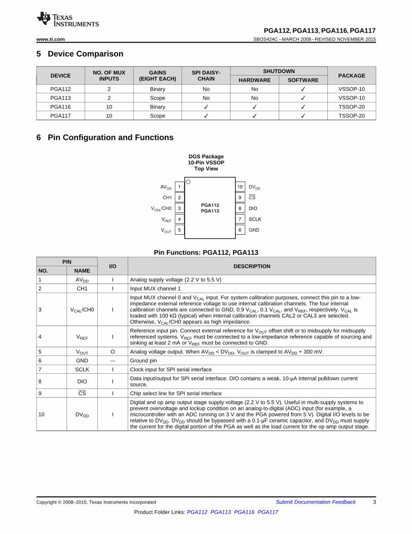
6 Pin Configuration and Functions
DGS Package10-Pin VSSOP
Top View
Pin Functions: PGA112, PGA113PIN
I/O DESCRIPTIONNO. NAME1 AVDD I Analog supply voltage (2.2 V to 5.5 V)2 CH1 I Input MUX channel 1
Input MUX channel 0 and VCAL input. For system calibration purposes, connect this pin to a low-impedance external reference voltage to use internal calibration channels. The four internal
3 VCAL/CH0 I calibration channels are connected to GND, 0.9 VCAL, 0.1 VCAL, and VREF, respectively. VCAL isloaded with 100 kΩ (typical) when internal calibration channels CAL2 or CAL3 are selected.Otherwise, VCAL/CH0 appears as high impedance.Reference input pin. Connect external reference for VOUT offset shift or to midsupply for midsupply
4 VREF I referenced systems. VREF must be connected to a low-impedance reference capable of sourcing andsinking at least 2 mA or VREF must be connected to GND.
5 VOUT O Analog voltage output. When AVDD < DVDD, VOUT is clamped to AVDD + 300 mV.6 GND — Ground pin7 SCLK I Clock input for SPI serial interface
Data input/output for SPI serial interface. DIO contains a weak, 10-μA internal pulldown current8 DIO I source.9 CS I Chip select line for SPI serial interface
Digital and op amp output stage supply voltage (2.2 V to 5.5 V). Useful in multi-supply systems toprevent overvoltage and lockup condition on an analog-to-digital (ADC) input (for example, a
10 DVDD I microcontroller with an ADC running on 3 V and the PGA powered from 5 V). Digital I/O levels to berelative to DVDD. DVDD should be bypassed with a 0.1-μF ceramic capacitor, and DVDD must supplythe current for the digital portion of the PGA as well as the load current for the op amp output stage.
Copyright © 2008–2015, Texas Instruments Incorporated Submit Documentation Feedback 3
Product Folder Links: PGA112 PGA113 PGA116 PGA117

AVDD
CH5
CH4
CH3
CH2
CH1
V /CH0CAL
VREF
VOUT
CH7
CH6
DVDD
CS
DOUT
DIN
SCLK
GND
ENABLE
CH9
CH8
1
2
3
4
5
6
7
8
9
10
20
19
18
17
16
15
14
13
12
11
PGA116
PGA117
PGA112, PGA113, PGA116, PGA117SBOS424C –MARCH 2008–REVISED NOVEMBER 2015 www.ti.com
PW Package20-Pin TSSOP
Top View
Pin Functions: PGA116, PGA117PIN
I/O DESCRIPTIONNO. NAME1 AVDD I Analog supply voltage (2.2 V to 5.5 V)2 CH5 I Input MUX channel 53 CH4 I Input MUX channel 44 CH3 I Input MUX channel 35 CH2 I Input MUX channel 26 CH1 I Input MUX channel 1
Input MUX channel 0 and VCAL input. For system calibration purposes, connect this pin to a low-impedance external reference voltage to use internal calibration channels. The four internal
7 VCAL/CH0 I calibration channels are connected to GND, 0.9 VCAL, 0.1 VCAL, and VREF, respectively. VCAL isloaded with 100 kΩ (typical) when internal calibration channels CAL2 or CAL3 are selected.Otherwise, VCAL/CH0 appears as high impedance.Reference input pin. Connect external reference for VOUT offset shift or to midsupply for midsupply
8 VREF I referenced systems. VREF must be connected to a low-impedance reference capable of sourcingand sinking at least 2 mA or to GND.
9 VOUT O Analog voltage output. When AVDD < DVDD, VOUT is clamped to AVDD + 300 mV.10 CH7 I Input MUX channel 711 CH8 I Input MUX channel 812 CH9 I Input MUX channel 913 ENABLE I Hardware enable pin. Logic low puts the part into Shutdown mode (IQ < 1 μA).14 GND — Ground pin15 SCLK I Clock input for SPI serial interface
Data input for SPI serial interface. DIN contains a weak, 10-μA internal pulldown current source to16 DIN I allow for ease of daisy-chain configurations.Data output for SPI serial interface. DOUT goes to high-Z state when CS goes high for standard17 DOUT O SPI interface.
18 CS I Chip select line for SPI serial interfaceDigital and op amp output stage supply voltage (2.2 V to 5.5 V). Useful in multi-supply systems toprevent overvoltage and lockup condition on an ADC input (for example, a microcontroller with an
19 DVDD I ADC running on 3 V and the PGA powered from 5 V). Digital I/O levels to be relative to DVDD. DVDDshould be bypassed with a 0.1-μF ceramic capacitor, and DVDD must supply the current for thedigital portion of the PGA as well as the load current for the op amp output stage.
20 CH6 I Input MUX channel 6
4 Submit Documentation Feedback Copyright © 2008–2015, Texas Instruments Incorporated
Product Folder Links: PGA112 PGA113 PGA116 PGA117
PGA112, PGA113, PGA116, PGA117www.ti.com SBOS424C –MARCH 2008–REVISED NOVEMBER 2015
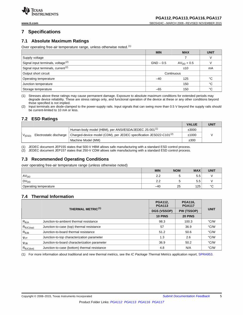
7 Specifications
7.1 Absolute Maximum RatingsOver operating free-air temperature range, unless otherwise noted. (1)
MIN MAX UNITSupply voltage 7 VSignal input terminals, voltage (2) GND – 0.5 AVDD + 0.5 VSignal input terminals, current (2) ±10 mAOutput short circuit ContinuousOperating temperature –40 125 °CJunction temperature 150 °CStorage temperature –65 150 °C
(1) Stresses above these ratings may cause permanent damage. Exposure to absolute maximum conditions for extended periods maydegrade device reliability. These are stress ratings only, and functional operation of the device at these or any other conditions beyondthose specified is not implied.
(2) Input terminals are diode-clamped to the power-supply rails. Input signals that can swing more than 0.5 V beyond the supply rails shouldbe current-limited to 10 mA or less.
7.2 ESD RatingsVALUE UNIT
Human-body model (HBM), per ANSI/ESDA/JEDEC JS-001 (1) ±3000V(ESD) Electrostatic discharge Charged-device model (CDM), per JEDEC specification JESD22-C101 (2) ±1000 V
Machine Model (MM) ±300
(1) JEDEC document JEP155 states that 500-V HBM allows safe manufacturing with a standard ESD control process.(2) JEDEC document JEP157 states that 250-V CDM allows safe manufacturing with a standard ESD control process.
7.3 Recommended Operating Conditionsover operating free-air temperature range (unless otherwise noted)
MIN NOM MAX UNITAVDD 2.2 5 5.5 VDVDD 2.2 5 5.5 VOperating temperature –40 25 125 °C
7.4 Thermal InformationPGA112, PGA116,PGA113 PGA117
THERMAL METRIC (1) UNITDGS (VSSOP) PW (TSSOP)10 PINS 20 PINS
RθJA Junction-to-ambient thermal resistance 98.3 100.3 °C/WRθJC(top) Junction-to-case (top) thermal resistance 57 36.9 °C/WRθJB Junction-to-board thermal resistance 51.2 50.6 °C/WψJT Junction-to-top characterization parameter 1.3 2.6 °C/WψJB Junction-to-board characterization parameter 36.9 50.2 °C/WRθJC(bot) Junction-to-case (bottom) thermal resistance 4.8 N/A °C/W
(1) For more information about traditional and new thermal metrics, see the IC Package Thermal Metrics application report, SPRA953.
Copyright © 2008–2015, Texas Instruments Incorporated Submit Documentation Feedback 5
Product Folder Links: PGA112 PGA113 PGA116 PGA117

PGA112, PGA113, PGA116, PGA117SBOS424C –MARCH 2008–REVISED NOVEMBER 2015 www.ti.com
7.5 Electrical Characteristics: VS = AVDD = DVDD = 5 Vat TA = 25°C, RL = 10kΩ//CL = 100 pF connected to DVDD/2, and VREF = GND (unless otherwise noted)
PARAMETER TEST CONDITIONS MIN TYP MAX UNIT
OFFSET VOLTAGE
Input offset voltage VOS AVDD = DVDD = 5 V, VREF = VIN = AVDD/2, VCM = 2.5 V ±25 ±100 μV
AVDD = DVDD = 5 V, VREF = VIN = AVDD/2, VCM = 4.5 V ±75 ±325 μV
vs temperature, –40°C to dVOS/dT AVDD = DVDD = 5 V, VCM = 2.5 V TA = –40°C to 125°C 0.35 1.2 μV/°C125°C
vs temperature, –40°C to 85°C AVDD = DVDD = 5 V, VCM = 2.5 V 0.15 0.9 μV/°C
vs temperature, –40°C to 125°C AVDD = DVDD = 5 V, VCM = 4.5 V TA = –40°C to 125°C 0.6 1.8 μV/°C
vs temperature, –40°C to 85°C AVDD = DVDD = 5 V, VCM = 4.5 V 0.3 1.3 μV/°C
AVDD = DVDD = 2.2 V to 5.5 V, VCM = 0.5 V,vs power supply PSRR 5 20 μV/VVREF = VIN = AVDD/2
AVDD = DVDD = 2.2 V to 5.5 V, VCM = 0.5 V,Over temperature, –40°C to 125°C TA = –40°C to 125°C 5 40 μV/VVREF = VIN = AVDD/2
INPUT ON-CHANNEL CURRENT
Input on-channel current (Ch0, IIN VREF = VIN = AVDD/2 ±1.5 ±5 nACh1)
Over temperature, –40°C to 125°C VREF = VIN = AVDD/2 See Typical Characteristics nA
INPUT VOLTAGE RANGE
Input voltage range(1) IVR GND – 0.1 AVDD + 0.1 V
Overvoltage input range No output phase reversal (2) GND – 0.3 AVDD + 0.3 V
INPUT IMPEDANCE (Channel On) (3)
Channel input capacitance CCH 2 pF
Channel switch resistance RSW 150 Ω
Amplifier input capacitance CAMP 3 pF
Amplifier input resistance RAMP Input resistance to GND 10 GΩ
VCAL/CH0 RIN CAL1 or CAL2 selected 100 kΩ
GAIN SELECTIONS
Nominal gains Binary gains: 1, 2, 4, 8, 16, 32, 64, 128 1 128
Scope gains: 1, 2, 5, 10, 20, 50, 100, 200 1 200
DC gain error G = 1 VOUT = GND + 85 mV to DVDD – 85 mV 0.006% 0.1%
1 < G ≤ 32 VOUT = GND + 85 mV to DVDD – 85 mV 0.1%
G ≥ 50 VOUT = GND + 85 mV to DVDD – 85 mV 0.3%
DC gain drift G = 1 VOUT = GND + 85 mV to DVDD – 85 mV TA = –40°C to 125°C 0.5 ppm/°C
1 < G ≤ 32 VOUT = GND + 85 mV to DVDD – 85 mV TA = –40°C to 125°C 2 ppm/°C
G ≥ 50 VOUT = GND + 85 mV to DVDD – 85 mV TA = –40°C to 125°C 6 ppm/°C
Op Amp + Input = 0.9 VCAL,CAL2 DC gain error (4) 0.02%VREF = VCAL = AVDD/2, G = 1
Op Amp + Input = 0.9 VCAL,CAL2 DC gain drift (4) TA = –40°C to 125°C 2 ppm/°CVREF = VCAL = AVDD/2, G = 1
Op Amp + Input = 0.1 VCAL,CAL3 DC gain error(4) 0.02%VREF = VCAL = AVDD/2, G = 1
Op Amp + Input = 0.1 VCAL,CAL3 DC gain drift (4) TA = –40°C to 125°C 2 ppm/°CVREF = VCAL = AVDD/2, G = 1
INPUT IMPEDANCE (CHANNEL OFF) (3)
Input impedance CCH See Figure 55 2 pF
(1) Gain error is a function of the input voltage. Gain error outside of the range (GND + 85 mV ≤ VOUT ≤ DVDD – 85 mV) increases to 0.5%(typical).
(2) Input voltages beyond this range must be current-limited to < |10 mA| through the input protection diodes on each channel to preventpermanent destruction of the device.
(3) See Figure 55.(4) Total VOUT error must be computed using input offset voltage error multiplied by gain. Includes op amp G = 1 error.
6 Submit Documentation Feedback Copyright © 2008–2015, Texas Instruments Incorporated
Product Folder Links: PGA112 PGA113 PGA116 PGA117

PGA112, PGA113, PGA116, PGA117www.ti.com SBOS424C –MARCH 2008–REVISED NOVEMBER 2015
Electrical Characteristics: VS = AVDD = DVDD = 5 V (continued)at TA = 25°C, RL = 10kΩ//CL = 100 pF connected to DVDD/2, and VREF = GND (unless otherwise noted)
PARAMETER TEST CONDITIONS MIN TYP MAX UNIT
INPUT OFF-CHANNEL CURRENT
Input Off-Channel Current (Ch0, VREF = GND, VOFF-CHANNEL = AVDD/2,ILKG ±0.05 ±1 nACh1)(5) VON-CHANNEL = AVDD/2 – 0.1 V
VREF = GND, VOFF-CHANNEL = AVDD/2,Over temperature, –40°C to 125°C See Typical CharacteristicsVON-CHANNEL = AVDD/2 – 0.1 V
Channel-to-Channel Crosstalk 130 dB
OUTPUT
Voltage output swing from rail IOUT = ±0.25 mA, AVDD ≥ DVDD(6) GND + 0.05 DVDD – 0.05 V
IOUT = ±5 mA, AVDD ≥ DVDD(6) GND + 0.25 DVDD – 0.25 V
DC output nonlinearity VOUT = GND + 85 mV to DVDD – 85 mV(7) 0.0015 %FSR
Short circuit current ISC –30/+60 mA
Capacitive load drive CLOAD See Typical Characteristics
NOISE
Input voltage noise density en f > 10 kHz, CL = 100 pF, VS = 5 V 12 nV/√Hz
f > 10 kHz, CL = 100 pF, VS = 2.2 V 22 nV/√Hz
Input voltage noise en f = 0.1 Hz to 10 Hz, CL = 100 pF, VS = 5 V 0.362 μVPP
f = 0.1 Hz to 10 Hz, CL = 100 pF, VS = 2.2 V 0.736 μVPP
Input current density In f = 10 kHz, CL = 100 pF 400 fA/√Hz
SLEW RATE
Slew rate SR See Table 1 V/μs
SETTLING TIME
Settling time tS See Table 1 μs
FREQUENCY RESPONSE
Frequency response See Table 1 MHz
THD + NOISE
G = 1, f = 1 kHz, VOUT = 4 VPP at 2.5VDC, CL = 100 pF 0.003%
G = 10, f = 1 kHz, VOUT = 4 VPP at 2.5VDC, CL = 100 pF 0.005%
G = 50, f = 1 kHz, VOUT = 4 VPP at 2.5VDC, CL = 100 pF 0.03%
G = 128, f = 1 kHz, VOUT = 4 VPP at 2.5VDC, CL = 100 pF 0.08%
G = 200, f = 1 kHz, VOUT = 4 VPP at 2.5VDC, CL = 100 pF 0.1%
G = 1, f = 20 kHz, VOUT = 4 VPP at 2.5VDC, CL = 100 pF 0.02%
G = 10, f = 20 kHz, VOUT = 4 VPP at 2.5VDC, CL = 100 pF 0.01%
G = 50, f = 20 kHz, VOUT = 4 VPP at 2.5VDC, CL = 100 pF 0.03%
G = 128, f = 20 kHz, VOUT = 4 VPP at 2.5VDC, CL = 100 pF 0.08%
G = 200, f = 20 kHz, VOUT = 4 VPP at 2.5VDC, CL = 100 pF 0.11%
POWER SUPPLY
Operating voltage range(6) AVDD 2.2 5.5 V
DVDD 2.2 5.5 V
Quiescent current analog IQA IO = 0, G = 1, VOUT = VREF 0.33 0.45 mA
Over temperature, –40°C to 125°C TA = –40°C to 125°C 0.45 mA
IO = 0, G = 1, VOUT = VREF, SCLK at 10 MHz,Quiescent current digital (8)(9)(10) IQD 0.75 1.2 mACS = Logic 0, DIO or DIN = Logic 0
IO = 0, G = 1, VOUT = VREF, SCLK at 10 MHz,Over temperature, –40°C to 125°C(8)(9)(10) TA = –40°C to 125°C 1.2 mACS = Logic 0, DIO or DIN = Logic 0
Shutdown current analog + ISDA + ISDD IO = 0, VOUT = VREF, G = 1, SCLK Idle 4 μAdigital(8)(9)
IO = 0, VOUT = 0, G = 1, SCLK at 10MHz, 245 μACS = Logic 0, DIO or DIN = Logic 0
POWER-ON RESET (POR)
Digital interface disabled and Command Register set to POR values forPOR trip voltage 1.6 VDVDD < POR Trip Voltage
(5) Maximum specification limitation limited by final test time and capability.(6) When AVDD is less than DVDD, the output is clamped to AVDD + 300 mV.(7) Measurement limited by noise in test equipment and test time.(8) Does not include current into or out of the VREF pin. Internal RF and RI are always connected between VOUT and VREF.(9) Digital logic levels: DIO or DIN = logic 0. 10-μA internal pulldown current source.(10) Includes current from op amp output structure.
Copyright © 2008–2015, Texas Instruments Incorporated Submit Documentation Feedback 7
Product Folder Links: PGA112 PGA113 PGA116 PGA117

PGA112, PGA113, PGA116, PGA117SBOS424C –MARCH 2008–REVISED NOVEMBER 2015 www.ti.com
Electrical Characteristics: VS = AVDD = DVDD = 5 V (continued)at TA = 25°C, RL = 10kΩ//CL = 100 pF connected to DVDD/2, and VREF = GND (unless otherwise noted)
PARAMETER TEST CONDITIONS MIN TYP MAX UNIT
TEMPERATURE RANGE
Specified range –40 125 °C
Operating range –40 125 °C
Thermal resistance θJA
VSSOP-10 164 °C/W
DIGITAL INPUTS (SCLK, CS, DIO, DIN)
Logic low 0 0.3DVDD V
Input leakage current (SCLK and CS only) –1 1 μA
Weak pulldown current (DIO, DIN only) 10 μA
Logic high 0.7DVDD DVDD V
Hysteresis 700 mV
DIGITAL OUTPUT (DIO, DOUT)
Logic high IOH = –3 mA (sourcing) DVDD – 0.4 DVDD V
Logic low IOL = 3 mA (sinking) GND GND + 0.4 V
CHANNEL AND GAIN TIMING
Channel select time 0.2 μs
Gain select time 0.2 μs
SHUTDOWN MODE TIMING
Enable time 4 μs
VOUT goes high-impedance, RF and RI remain connected between VOUT andDisable time 2 μsVREF
POWER-ON-RESET (POR) TIMING
POR power-up time DVDD ≥ 2 V 40 μs
POR power-down time DVDD ≤ 1.5 V 5 μs
8 Submit Documentation Feedback Copyright © 2008–2015, Texas Instruments Incorporated
Product Folder Links: PGA112 PGA113 PGA116 PGA117

CS
SCLK
DIN
DOUT
Hi-Z Hi-Z
tCSH
tSCCS
tLO
tCSSC
tSU tHD
tDO tSOZ
tHI
tCS1 tCS0
1/fSCLK
PGA112, PGA113, PGA116, PGA117www.ti.com SBOS424C –MARCH 2008–REVISED NOVEMBER 2015
7.6 SPI Timing: VS = AVDD = DVDD = 2.2 V to 5 VAt TA = +25°C, RL = 10kΩ//CL = 100pF connected to DVDD/2, and VREF = GND, unless otherwise noted.
MIN NOM MAX UNITInput capacitance (SCLK, CS, and DIO pins) 1 pFInput rise and fall time (1)
tRFI 2 μs(CS, SCLK, and DIO pins)tRFO Output rise and fall time (DIO pin) (1) CLOAD = 60 pF 10 nstCSH CS high time (CS pin) (1) 40 nstCSO SCLK edge to CS fall setup time (1) 10 nstCSSC CS fall to first SCLK edge setup time 10 nsfSCLK SCLK Frequency (2) 10 MHztHI SCLK high time (3) 40 nstLO SCLK low time (3) 40 nstSCCS SCLK last edge to CS rise setup time (1) 10 nstCS1 CS rise to SCLK edge setup time (1) 10 nstSU DIN setup time 10 nstHD DIN hold time 10 nstDO SCLK to DOUT valid propagation delay (1) 25 nstSOZ CS rise to DOUT forced to Hi-Z (1) 20 ns
(1) Ensured by design; not production tested.(2) When using devices in daisy-chain mode, the maximum clock frequency for SCLK is limited by SCLK rise and fall time, DIN setup time,
and DOUT propagation delay. See Figure 61. Based on this limitation, the maximum SCLK frequency for daisy-chain mode is 9.09 MHz.(3) tHI and tLO must not be less than 1/SCLK (maximum).
Figure 1. SPI Mode 0, 0
Copyright © 2008–2015, Texas Instruments Incorporated Submit Documentation Feedback 9
Product Folder Links: PGA112 PGA113 PGA116 PGA117

CS
SCLK
DIN
DOUT
tCSSC
tHI tLO
tSCCS tCS1
tSOZtDO
tCS0
tSU tHD
1/fSCLK
Hi-Z Hi-Z
tCSH
PGA112, PGA113, PGA116, PGA117SBOS424C –MARCH 2008–REVISED NOVEMBER 2015 www.ti.com
Figure 2. SPI Mode 1, 1
10 Submit Documentation Feedback Copyright © 2008–2015, Texas Instruments Incorporated
Product Folder Links: PGA112 PGA113 PGA116 PGA117
-0.9
6
Offset Voltage Drift ( V/ C)m °
Popula
tion
-1.0
8
-1.2
0
-0.8
4
-0.7
2
-0.1
2
-0.2
4
-0.3
6
-0.4
8
-0.6
0 0
0.1
2
1.0
8
1.2
0
0.9
6
0.2
4
0.3
6
0.4
8
0.8
4
0.7
2
0.6
0
V = 2.5VCM
-1
.44
Offset Voltage Drift ( V/ C)m °
Po
pu
latio
n
-1
.80
-1
.26
-1
.08
-0
.18
-0
.36
-0
.54
-0
.72
-0
.90 0
0.1
8
1.6
2
1.4
4
0.3
6
0.5
4
0.7
2
1.2
6
1.0
8
0.9
0
1.8
0V = 4.5VCM
-1
.62
-0.7
2
Offset Voltage Drift ( V/ C)m °
Popula
tion
-0.8
1
-0.9
0
-0.6
3
-0.5
4
-0.0
9
-0.1
8
-0.2
7
-0.3
6
-0.4
5 0
0.0
9
0.8
1
0.9
0
0.7
2
0.1
8
0.2
7
0.3
6
0.6
3
0.5
4
0.4
5
V = 2.5VCM
-1.0
4
Offset Voltage Drift ( V/ C)m °
Popula
tion
-1.3
0
-0.9
1
-0.7
8
-0.1
3
-0.2
6
-0.3
9
-0.5
2
-0.6
5 0
0.1
3
1.1
7
1.0
4
0.2
6
0.3
9
0.5
2
0.9
1
0.7
8
0.6
5
1.3
0
V = 4.5VCM
-1.1
7
-260.0
Offset Voltage ( V)m
Popula
tion
-325.0
-227.5
-195.0
-32.5
-65.0
-97.5
-130.0
-162.5 0
32.5
292.5
260.0
65.0
97.5
130.0
227.5
195.0
162.5
V = 4.5VCM
325.0
-292.5
-80
Offset Voltage ( V)m
Popula
tion
-90
-100
-70
-60
-10
-20
-30
-40
-50 0
10
90
100
80
20
30
40
70
60
50
V = 2.5VCM
PGA112, PGA113, PGA116, PGA117www.ti.com SBOS424C –MARCH 2008–REVISED NOVEMBER 2015
7.7 Typical Characteristicsat TA = 25°C, AVDD = DVDD = 5 V, RL = 10 kΩ connected to DVDD/2, VREF = GND, and CL = 100 pF, unless otherwise noted.
Figure 4. Offset VoltageFigure 3. Offset Voltage
Figure 5. Offset Voltage Drift (–40°C to 85°C) Figure 6. Offset Voltage Drift (–40°C to 85°C)
Figure 8. Offset Voltage Drift (–40°C to 125°C)Figure 7. Offset Voltage Drift (–40°C to 125°C)
Copyright © 2008–2015, Texas Instruments Incorporated Submit Documentation Feedback 11
Product Folder Links: PGA112 PGA113 PGA116 PGA117

-0.2
40
Gain Error (%)
Popula
tion
-0.2
70
-0.3
00
-0.2
10
-0.1
80
-0.0
30
-0.0
60
-0.0
90
-0.1
20
-0.1
50 0
0.0
30
0.2
70
0.2
40
0.0
60
0.0
90
0.1
20
0.2
10
0.1
80
0.1
50
0.3
00
Gain Error Drift ( )ppm/ C°
Popula
tion
G = 1
0.1
0
0.0
50
0.1
5
0.2
0
0.4
5
0.4
0
0.3
5
0.3
0
0.2
5
0.5
0
0.5
5
0.9
5
0.9
0
0.6
0
0.6
5
0.7
0
0.8
5
0.8
0
0.7
5
1.0
0
-0
.08
Gain Error (%)
Po
pu
latio
n
-0
.09
-0
.10
-0
.07
-0
.06
-0
.01
-0
.02
-0
.03
-0
.04
-0
.05 0
0.0
1
0.0
9
0.0
8
0.0
2
0.0
3
0.0
4
0.0
7
0.0
6
0.0
5
0.1
0
-0
.08
Gain Error (%)
Po
pu
latio
n
-0
.09
-0
.10
-0
.07
-0
.06
-0
.01
-0
.02
-0
.03
-0
.04
-0
.05 0
0.0
1
0.0
9
0.0
8
0.0
2
0.0
3
0.0
4
0.0
7
0.0
6
0.0
5
0.1
0
0 1 5
Input Voltage (V)
100
80
60
40
20
0
20
40
60
80
100
-
-
-
-
-
Input O
ffset V
oltage (
V)
m
32 4
V (V)OUT
DC
Outp
ut N
onlin
earity
Err
or
(%F
SR
)
0.0010
0.0008
0.0006
0.0004
0.0002
0
0.0002
0.0004
0.0006
0.0008
0.0010
-
-
-
-
-
0.50 5.01.0 1.5
G = 128
G = 16
G = 2G = 1
2.0 2.5 3.0 3.5 4.0 4.5
AV = DV = +5VDD DD
PGA112, PGA113, PGA116, PGA117SBOS424C –MARCH 2008–REVISED NOVEMBER 2015 www.ti.com
Typical Characteristics (continued)at TA = 25°C, AVDD = DVDD = 5 V, RL = 10 kΩ connected to DVDD/2, VREF = GND, and CL = 100 pF, unless otherwise noted.
Figure 9. Input Offset Voltage vs Input Voltage Figure 10. PGA112 and PGA116 Nonlinearity
Figure 11. Gain Error (G = 1) Figure 12. Gain Error (1 < G ≤ 32)
Figure 13. Gain Error (G ≥ 50) Figure 14. Gain Error Drift (–40°C to 125°C)
12 Submit Documentation Feedback Copyright © 2008–2015, Texas Instruments Incorporated
Product Folder Links: PGA112 PGA113 PGA116 PGA117

-1
.6
Gain Error Drift (ppm/ C)°
Po
pu
latio
n
-2
.0
-1
.4
-1
.2
-0
.2
-0
.4
-0
.6
-0
.8
-1
.0 0
0.2
1.8
1.6
0.4
0.6
0.8
1.4
1.2
1.0
2.0
-1
.8
-1
.6
Gain Error Drift (ppm/ C)°
Po
pu
latio
n
-2
.0
-1
.4
-1
.2
-0
.2
-0
.4
-0
.6
-0
.8
-1
.0 0
0.2
1.8
1.6
0.4
0.6
0.8
1.4
1.2
1.0
> 2
.0
-1
.8
2.0
-0.0
8
Gain Error (%)
Popula
tion
-0.1
0
-0.0
7
-0.0
6
-0.0
1
-0.0
2
-0.0
3
-0.0
4
-0.0
5 0
0.0
1
0.0
9
0.0
8
0.0
2
0.0
3
0.0
4
0.0
7
0.0
6
0.0
5
0.1
0
-0.0
9
-0.0
8
Gain Error (%)
Popula
tion
-0.1
0
-0.0
7
-0.0
6
-0.0
1
-0.0
2
-0.0
3
-0.0
4
-0.0
5 0
0.0
1
0.0
9
0.0
8
0.0
2
0.0
3
0.0
4
0.0
7
0.0
6
0.0
5
0.1
0
-0.0
9
0.5
0
Gain Error Drift (ppm/ C)°
Popula
tion
0.2
50
0.7
5
1.0
0
2.2
5
2.0
0
1.7
5
1.5
0
1.2
5
2.5
0
2.7
5
4.7
5
4.5
0
3.0
0
3.2
5
3.5
0
4.2
5
4.0
0
3.7
5
5.0
0
1 G 32< £
1.0
Gain Error Drift (ppm/ C)°
Popula
tion
0.50
1.5
2.0
4.5
4.0
3.5
3.0
2.5
5.0
5.5
9.5
9.0
6.0
6.5
7.0
8.5
8.0
7.5
10.0
G 50³
PGA112, PGA113, PGA116, PGA117www.ti.com SBOS424C –MARCH 2008–REVISED NOVEMBER 2015
Typical Characteristics (continued)at TA = 25°C, AVDD = DVDD = 5 V, RL = 10 kΩ connected to DVDD/2, VREF = GND, and CL = 100 pF, unless otherwise noted.
Figure 15. Gain Error Drift (–40°C to 125°C)Figure 16. Gain Error Drift (–40°C to 125°C)
Figure 17. CAL2 Gain Error Figure 18. CAL3 Gain Error
Figure 19. CAL2 Gain Error Drift (–40°C to 125°C) Figure 20. CAL3 Gain Error Drift (–40°C to 125°C)
Copyright © 2008–2015, Texas Instruments Incorporated Submit Documentation Feedback 13
Product Folder Links: PGA112 PGA113 PGA116 PGA117

Frequency (Hz)
TH
D+
N (
%)
1
0.1
0.01
0.001
0.0001
10010 100k1k 10k
G = 128G = 64 G = 32 G = 16
G = 8
G = 4G = 2
G = 1
Frequency (Hz)
TH
D+
N (
%)
1
0.1
0.01
0.001
0.0001
10010 100k1k 10k
G = 1
G = 200 G = 100 G = 50 G = 20
G = 10G = 2
G = 5
1 10 100 1k 100k
Frequency (Hz)
100
10
Vo
lta
ge
No
ise
(n
V/
)ÖH
z
10k
1k
100
Cu
rren
t No
ise
(fA/
)ÖH
z
Voltage Noise, V = 5VS
Voltage Noise, V = 2.2VS
Current Noise, V = 5VS
50
20
500
200
Frequency (Hz)
TH
D+
N (
%)
1
0.1
0.01
0.001
0.0001
10010 100k1k 10k
G = 128G = 64 G = 32 G = 16
G = 8G = 2G = 1 G = 4
2.5s/div
25
0n
V/d
iv
V = 2.2VS
2.5s/div
10
0n
V/d
iv
V = 5VS
PGA112, PGA113, PGA116, PGA117SBOS424C –MARCH 2008–REVISED NOVEMBER 2015 www.ti.com
Typical Characteristics (continued)at TA = 25°C, AVDD = DVDD = 5 V, RL = 10 kΩ connected to DVDD/2, VREF = GND, and CL = 100 pF, unless otherwise noted.
Figure 21. 0.1 Hz To 10 Hz NOISE Figure 22. 0.1 Hz to 10 Hz NOISE
Figure 24. PGA112, PGA116 THD + Noise vs FrequencyFigure 23. Spectral NOISE Density(VOUT = 2 VPP)
Figure 25. PGA112, PGA116 THD + NOISE vs Frequency Figure 26. PGA113, PGA117 THD + Noise vs Frequency(VOUT = 4 VPP) (VOUT = 2 VPP)
14 Submit Documentation Feedback Copyright © 2008–2015, Texas Instruments Incorporated
Product Folder Links: PGA112 PGA113 PGA116 PGA117

0 2 4 6 8 10 12 14 16 18 24
Output Current (mA)
2.2
2.0
1.8
1.6
1.4
1.2
1.0
0.8
0.6
0.4
0.2
0
Ou
tpu
t V
olta
ge
(V
)
2220
V = 2.2V
G = 1S
+125 C° +25 C°
- °40 C
0 10 20 30 40 50 60 70 80 90 100
Output Current (mA)
5.5
5.0
4.5
4.0
3.5
3.0
2.5
2.0
1.5
1.0
0.5
0
Outp
ut V
oltage (
V)
V = 5.5V
G = 1S
+125 C°
+25 C°
- °40 C
Supply Voltage (V)
I+
I(m
A)
QA
QD
1.2
1.0
0.8
0.6
0.4
0.2
0
4.52.52.0 5.0 5.53.0 3.5 4.0
SCLK = 10MHzSCLK = 5MHz
SCLK = 2MHzSCLK = 500kHz
-50 -25 0 125
Temperature ( C)°
4.0
3.5
3.0
2.5
2.0
1.5
1.0
0.5
0
Shutd
ow
n I
(A
)m
Q
25 50 75 100
Digital
Analog
Frequency (Hz)
TH
D+
N (
%)
1
0.1
0.01
0.001
0.0001
10010 100k1k 10k
G = 200 G = 100 G = 50G = 20
G = 10G = 2
G = 1
G = 5
Temperature ( C)°
I(m
A)
Q
0.8
0.4
0.3
0.2
0.1
075-25-50 100 1250 25 50
0.5
0.6
0.7
V = 5.5VS
V = 2.2VS
Digital
Analog
f = 10MHzSCLK
PGA112, PGA113, PGA116, PGA117www.ti.com SBOS424C –MARCH 2008–REVISED NOVEMBER 2015
Typical Characteristics (continued)at TA = 25°C, AVDD = DVDD = 5 V, RL = 10 kΩ connected to DVDD/2, VREF = GND, and CL = 100 pF, unless otherwise noted.
Figure 27. PGA113, PGA117 THD + Noise vs Frequency Figure 28. Quiescent Current vs Temperature(VOUT = 4 VPP)
Figure 29. Total Quiescent Current vs Supply Voltage Figure 30. Shutdown Quiescent Current vs Temperature
Figure 32. Output Voltage vs Output CurrentFigure 31. Output Voltage vs Output Current
Copyright © 2008–2015, Texas Instruments Incorporated Submit Documentation Feedback 15
Product Folder Links: PGA112 PGA113 PGA116 PGA117

1k 10k 100k 1M 10M
Frequency (Hz)
2.5
2.0
1.5
1.0
0.5
0
Ou
tpu
t V
olta
ge
(V
)
G = 10
G = 2
G = 1
G = 5
AV = DVDD DD = 2.2V
1k 10k 100k 1M 10M
Frequency (Hz)
2.5
2.0
1.5
1.0
0.5
0
Ou
tpu
t V
olta
ge
(V
)
G = 100
G = 20
G = 200
G = 50
AV = DVDD DD = 2.2V
100 1k 10k 10M
Frequency (Hz)
6
5
4
3
2
1
0
Outp
ut V
oltage (
V)
100k 1M
G = 1
G = 8
G = 4
G = 2
AV = DV = 5.5VDD DD
100 1k 10k 10M
Frequency (Hz)
6
5
4
3
2
1
0
Outp
ut V
oltage (
V)
100k 1M
G = 128
G = 16
G = 64
G = 32
AV = DV = 5.5VDD DD
1k 10k 10M
Frequency (Hz)
2.5
2.0
1.5
1.0
0.5
0
Outp
ut V
oltage (
V)
100k 1M
G = 1
G = 8
G = 4
G = 2
AV = DV = 2.2VDD DD
1k 10k 10M
Frequency (Hz)
2.5
2.0
1.5
1.0
0.5
0
Outp
ut V
oltage (
V)
100k 1M
G = 128
G = 16
G = 64
G = 32
AV = 2.2VDD DV =DD
PGA112, PGA113, PGA116, PGA117SBOS424C –MARCH 2008–REVISED NOVEMBER 2015 www.ti.com
Typical Characteristics (continued)at TA = 25°C, AVDD = DVDD = 5 V, RL = 10 kΩ connected to DVDD/2, VREF = GND, and CL = 100 pF, unless otherwise noted.
Figure 33. PGA112, PGA116 Output Voltage Swing vs Figure 34. PGA112, PGA116 Output Voltage Swing vsFrequency Frequency
Figure 35. PGA112, PGA116 Output Voltage Swing vs Figure 36. PGA112, PGA116 Output Voltage Swing vsFrequency Frequency
Figure 37. PGA113, PGA117 Output Voltage Swing vs Figure 38. PGA113, PGA117 Output Voltage Swing vsFrequency Frequency
16 Submit Documentation Feedback Copyright © 2008–2015, Texas Instruments Incorporated
Product Folder Links: PGA112 PGA113 PGA116 PGA117

-50 -25 0 25 50 75 100 125
Temperature (°C)
25
20
15
10
5
0
5-
Input O
n-C
hannel C
urr
ent (n
A)
CH1 to
CH9
CH0
Measurement made with channel pin
connected to midsupply
Ch
an
ne
l 1 to
Ch
an
ne
l 9
Inp
ut O
ff-Ch
an
ne
l Cu
rren
t (nA
)
-50 -25 0 25 50 75 100 125
Temperature (°C)
25
20
15
10
5
0
5-
0.15
0.10
0.05
0
0.05
0.01
0.15
-
-
-Ch
an
ne
l 0
In
pu
t O
ff-C
ha
nn
el C
urr
en
t (n
A)
CH1 to
CH9
CH0
Measurement made with channel pin
connected to midsupply
0 50 100 200
Gain
12
10
8
6
4
2
0
Settlin
g T
ime (
s)
m
150
0.01%
0.1%
C = 100pF//R = 10kWL L
OUT PPV = 4V
0 100 200 300 400 500 600 700 800
Load Capacitance (pF)
50
40
30
20
10
0
Overs
hoot (%
)
G = 1
G 2>
100 1k 10k 100k 1M 10M
Frequency (Hz)
6
5
4
3
2
1
0
Ou
tpu
t V
olta
ge
(V
)
G = 10
G = 2
G = 1
G = 5
AV = DVDD DD = 5.5V
100 1k 10k 100k 1M 10M
Frequency (Hz)
6
5
4
3
2
1
0
Ou
tpu
t V
olta
ge
(V
)
G = 20
G = 200
G = 100
G = 50
AV = DVDD DD = 5.5V
PGA112, PGA113, PGA116, PGA117www.ti.com SBOS424C –MARCH 2008–REVISED NOVEMBER 2015
Typical Characteristics (continued)at TA = 25°C, AVDD = DVDD = 5 V, RL = 10 kΩ connected to DVDD/2, VREF = GND, and CL = 100 pF, unless otherwise noted.
Figure 39. PGA113, PGA117 Output Voltage Swing vs Figure 40. PGA113, PGA117 Output Voltage Swing vsFrequency Frequency
Figure 41. Small-Signal Overshoot vs Load Capacitance Figure 42. Gain vs Settling Time
Figure 44. Input OFF-Channel Leakage Current vsFigure 43. Input ON-Channel Current vs TemperatureTemperature
Copyright © 2008–2015, Texas Instruments Incorporated Submit Documentation Feedback 17
Product Folder Links: PGA112 PGA113 PGA116 PGA117

2.5 s/divm
2V
/div
G = 10
G = 2
G = 1
Output
Input
2.5 s/divm
2V
/div
Input
G = 50
G = 100, 200Output
2.5 s/divm
G = 20
G = 10
G = 1100mV
Output
Input
0V
V /GIN
0V
2.5 s/divm
Output
Input
G = 50
G = 100, 200
100mV
0V
V /GIN
0V
0.1 1 10 100 10M
Frequency (Hz)
110
100
90
80
70
60
50
40
30
20
10
0
PS
RR
(dB
)
1M100k10k1k
G = 200
G = 50
G = 10
G = 2
G = 1
G 2³
10 100 1k 10k 10M
Frequency (Hz)
140
130
120
110
100
90
80
70
60
Cro
ssta
lk (
dB
)
1M100k
PGA112, PGA113, PGA116, PGA117SBOS424C –MARCH 2008–REVISED NOVEMBER 2015 www.ti.com
Typical Characteristics (continued)at TA = 25°C, AVDD = DVDD = 5 V, RL = 10 kΩ connected to DVDD/2, VREF = GND, and CL = 100 pF, unless otherwise noted.
Figure 46. Crosstalk vs FrequencyFigure 45. Power-Supply Rejection Ratio vs Frequency
Figure 47. Small-Signal Pulse Response Figure 48. Small-Signal Pulse Response
Figure 49. Large-Signal Pulse Response Figure 50. Large-Signal Pulse Response
18 Submit Documentation Feedback Copyright © 2008–2015, Texas Instruments Incorporated
Product Folder Links: PGA112 PGA113 PGA116 PGA117

2V
/div
10 s/divm
Output
Enable
10 s/divm
2V
/div Output
ActiveIn
Shutdown
CS
Output
CS
In
Shutdown
Active
25 s/divm
0V
0V
Output (1V/div)
Supply (5V/div)
1ms/div
1V
/div
V = 5V
R = 10k
C = 100pF
S
L W
L
VIN
VOUT
5V
0V
PGA112, PGA113, PGA116, PGA117www.ti.com SBOS424C –MARCH 2008–REVISED NOVEMBER 2015
Typical Characteristics (continued)at TA = 25°C, AVDD = DVDD = 5 V, RL = 10 kΩ connected to DVDD/2, VREF = GND, and CL = 100 pF, unless otherwise noted.
Figure 51. Power-Up and Power-Down Timing Figure 52. Output Overdrive Performance
Figure 53. Output Voltage vs Shutdown Mode Figure 54. PGA116, PGA117 Hardware Shutdown Mode
Copyright © 2008–2015, Texas Instruments Incorporated Submit Documentation Feedback 19
Product Folder Links: PGA112 PGA113 PGA116 PGA117

Output Stage
SPI Interface
CAL2CAL3
CAL4
10
+
±CAL1
RF
R1
0.9VCAL
0.1VCAL
VCAL/CH0CH1
AVDD DVDD
VOUT
SCLK
DIO
VREF
VREF
CAL2/3
MUX
CS
GND
10 k
80 k
PGA112, PGA113, PGA116, PGA117SBOS424C –MARCH 2008–REVISED NOVEMBER 2015 www.ti.com
8 Detailed Description
8.1 OverviewThe PGA112 and PGA113 devices (binary and scope gains) offer two analog inputs, a three-pin SPI interface,and software shutdown in an 10-pin VSSOP package. The PGA116 and PGA117 (binary and scope gains) offer10 analog inputs, and hardware and software shutdown in a 20-pin TSSOP package.
All versions provide internal calibration channels for system-level calibration. The channels are tied to GND, 0.9VCAL, 0.1 VCAL, and VREF, respectively. VCAL, an external voltage connected to Channel 0, is used as the systemcalibration reference. Binary gains are: 1, 2, 4, 8, 16, 32, 64, and 128; scope gains are: 1, 2, 5, 10, 20, 50, 100,and 200.
The PGA uses a SPI interface with daisy-chain capability, a standard serial peripheral interface (SPI). Both SPIMode 0,0 and Mode 1,1 are supported, as shown in Figure 56 and described in Table 2.
8.2 Functional Block Diagram
8.3 Feature DescriptionFeaturing low offset, low offset drift and low noise, the PGA11x series provides a flexible analog building blockfor a variety of applications. The PGA112 and PGA116 offer binary gains of 1, 2, 4, 8, 16, 32, 64, 128 and a 2channel MUX while the PGA113 and PGA117 offer scope gains of 1, 2, 5, 10, 20, 50, 100, 200 and a 10 channelMUX.
8.4 Device Functional ModesThe PGA112 and PGA113 devices have a software shutdown mode, and the PGA116 and PGA117 devices offerboth a hardware and software shutdown mode, see Shutdown and Power-On-Reset (POR) for additionalinformation. The PGA uses a standard serial peripheral interface (SPI). Both SPI Mode 0,0 and Mode 1,1 aresupported. More information regarding serial communications, including daisy chaining can be found in SerialInterface Information.
20 Submit Documentation Feedback Copyright © 2008–2015, Texas Instruments Incorporated
Product Folder Links: PGA112 PGA113 PGA116 PGA117

1 2 3 4 5 6 7 8 9 10 11 12 13 14 15 16
CS
SCLK
DIN
DOUT
SPI Mode 0, 0 (CPOL = 0, CPHA = 0)
CS
SCLK
DIN
DOUT
1 2 3 4 5 6 7 8 9 10 11 12 13 14 15 16
SPI Mode 1, 1 (CPOL = 1, CPHA = 1)
RSW
RAMP
RF
RI
Mux
Switch
CCH CAMPVOUT
CHx
(Input)
VREF
Break-Before-Make
PGA112, PGA113, PGA116, PGA117www.ti.com SBOS424C –MARCH 2008–REVISED NOVEMBER 2015
8.5 Programming
Table 1. Frequency Response Versus Gain (CL = 100 pf, RL= 10 kω)0.1% 0.01% 0.1% 0.01%TYPICAL SLEW SLEW TYPICAL SLEW SLEWSETTLING SETTLING SCOPE SETTLING SETTLINGBINARY –3-dB RATE- RATE- –3-dB RATE- RATE-TIME: TIME: GAIN TIME: TIME:GAIN (V/V) FREQUENCY FALL RISE FREQUENCY FALL RISE4 VPP 4 VPP (V/V) 4 VPP 4 VPP(MHz) (V/μs) (V/μs) (MHz) (V/μs) (V/μs)(μs) (μs) (μs) (μs)
1 10 8 3 2 2.55 1 10 8 3 2 2.55
2 3.8 9 6.4 2 2.6 2 3.8 9 6.4 2 2.6
4 2 12.8 10.6 2 2.6 5 1.8 12.8 10.6 2 2.6
8 1.8 12.8 10.6 2 2.6 10 1.8 12.8 10.6 2.2 2.6
16 1.6 12.8 12.8 2.3 2.6 20 1.3 12.8 9.1 2.3 2.8
32 1.8 12.8 13.3 2.3 3 50 0.9 9.1 7.1 2.4 3.8
64 0.6 4 3.5 3 6 100 0.38 4 3.5 4.4 7
128 0.35 2.5 2.5 4.8 8 200 0.23 2.3 2 6.9 10
Figure 55. Equivalent Input Circuit
8.6 Serial Interface Information
Figure 56. SPI Mode 0,0 And Mode 1,1
Copyright © 2008–2015, Texas Instruments Incorporated Submit Documentation Feedback 21
Product Folder Links: PGA112 PGA113 PGA116 PGA117

10 Am
PGA112
PGA113
DOUT
DIO
DIN
10 Am
PGA116
PGA117
DOUT
DIN
PGA112, PGA113, PGA116, PGA117SBOS424C –MARCH 2008–REVISED NOVEMBER 2015 www.ti.com
Serial Interface Information (continued)Table 2. SPI Mode Setting Description
MODE CPOL CPHA CPOL DESCRIPTION CPHA DESCRIPTION
0, 0 0 0 (1) Clock idles low Data are read on the rising edge of clock. Data change on the falling edge of clock.
1, 1 1 1 (2) Clock idles high Data are read on the rising edge of clock. Data change on the falling edge of clock.
(1) CPHA = 0 means sample on first clock edge (rising or falling) after a valid CS.(2) CPHA = 1 means sample on second clock edge (rising or falling) after a valid CS.
8.6.1 Serial Digital Interface: SPI ModesThe PGA uses a standard serial peripheral interface (SPI). Both SPI Mode 0,0 and Mode 1,1 are supported, asshown in Figure 56 and described in Table 2.
If there are not even-numbered increments of 16 clocks (that is, 16, 32, 64, and so forth) between CS going low(falling edge) and CS going high (rising edge), the device takes no action. This condition provides reliable serialcommunication. Furthermore, this condition also provides a way to quickly reset the SPI interface to a knownstarting condition for data synchronization. Transmitted data are latched internally on the rising edge of CS.
On the PGA116 and PGA117 devices, CS, DIN, and SCLK are Schmitt-triggered CMOS logic inputs. DIN has aweak internal pulldown to support daisy-chain communications on the PGA116 and PGA117 devices. DOUT is aCMOS logic output. When CS is high, the state of DOUT is high-impedance. When CS is low, DOUT is driven asillustrated in Figure 57.
Figure 57. Digital I/O Structure—PGA116 and PGA117
On the PGA112 and PGA113 devices, there are digital output and digital input gates both internally connected tothe DIO pin. DIN is an input-only gate and DOUT is a digital output that can give a 3-state output. The DIO pinhas a weak 10-μA pulldown current source to prevent the pin from floating in systems with a high-impedance SPIDOUT line. When CS is high, the state of the internal DOUT gate is high-impedance. When CS is low, the stateof DIO depends on the previous valid SPI communication; either DIO becomes an output to clock out data or itremains an input to receive data. This structure is shown in Figure 58.
Figure 58. Digital I/O Structure—PGA112 and PGA113
22 Submit Documentation Feedback Copyright © 2008–2015, Texas Instruments Incorporated
Product Folder Links: PGA112 PGA113 PGA116 PGA117

CS
DOUT
SCLK
DINMSP430
CS
SCLK
DIN1 DOUT1
U1 CS
SCLK
DIO
U2
PGA116/PGA117 PGA112/PGA113
CS
DOUT
SCLK
DINMSP430
CS
SCLK
DIN1 DOUT1
U1 CS
SCLK
DIN2 DOUT2
U2
PGA116/PGA117 PGA116/PGA117
PGA112, PGA113, PGA116, PGA117www.ti.com SBOS424C –MARCH 2008–REVISED NOVEMBER 2015
8.6.2 Serial Digital Interface: SPI Daisy-Chain CommunicationsTo reduce the number of I/O port pins used on a microcontroller, the PGA116 and PGA117 support SPI daisy-chain communications with full read and write capability. A two-device daisy-chain configuration is shown inFigure 59, although any number of devices can be daisy-chained. The SPI daisy-chain communication uses acommon SCLK and CS line for all devices in the daisy chain, rather than each device requiring a separate CSline. The daisy-chain mode of communication routes data serially through each device in the chain by using itsrespective DIN and DOUT pins as shown. Special commands are used (see Table 4) to ensure that data arewritten or read in the proper sequence. There is a special daisy-chain NOP command (No OPeration) which,when presented to the desired device in the daisy-chain, causes no changes in that respective device. Detailedtiming diagrams for daisy-chain operation are shown in Figure 63 through Figure 65.
Figure 59. Daisy-Chain Read and Write Configuration
The PGA112 and PGA113 devices can be used as the last device in a daisy-chain as shown in Figure 60 ifwrite-only communication is acceptable, because the PGA112 and PGA113 devices have no separate DOUT pinto connect back to the microcontroller DIN pin to read back data in this configuration.
Figure 60. Daisy-Chain Write-Only Configuration
The maximum SCLK frequency that can be used in daisy-chain operation is directly related to SCLK rise and falltimes, DIN setup time, and DOUT propagation delay. Any number of two or more devices have the samelimitations because it is the timing considerations between adjacent devices that limit the clock speed.
Figure 61 analyzes the maximum SCLK frequency for daisy-chain mode based on the circuit of Figure 59. Aclock rise and fall time of 10 ns is assumed to allow for extra bus capacitance that could occur as a result ofmultiple devices in the daisy-chain.
Copyright © 2008–2015, Texas Instruments Incorporated Submit Documentation Feedback 23
Product Folder Links: PGA112 PGA113 PGA116 PGA117

SCLK
DOUT1
DIN2
tRFI
tSU
tMIN
= 55ns
SCLKMAX
= 9.09MHz
tMIN
= 55ns
tDO
tRFI
10ns
10ns
25ns
10ns
PGA112, PGA113, PGA116, PGA117SBOS424C –MARCH 2008–REVISED NOVEMBER 2015 www.ti.com
Figure 61. Daisy-Chain Maximum SCLK Frequency
24 Submit Documentation Feedback Copyright © 2008–2015, Texas Instruments Incorporated
Product Folder Links: PGA112 PGA113 PGA116 PGA117

Hi-Z
CS
SCLK
DIN
DOUT
SPI Read, Mode = 1, 1
1 2 3 4 5 6 7 8 9 10 11 12 13 14 15 16
0 1 1 0 1 0 1
17 18 19 20 21 22 23 24 25 26 27 28 29 30 31 32
0 0 0 0 0 0 0 0Hi-Z
0 0 0 0 0 0 0 0 0
D15 D14 D13 D12 D11 D10 D9 D8 D7 D6 D5 D4 D3 D2 D1 D0
D7 D0D6 D5 D4 D3 D2 D1
G3 G2 G1 G0 CH3 CH2 CH1 CH0
D15 D14 D13 D12 D11 D10 D9 D8
DIO
Pin
1 2 3 4 5 6 7 8 9 10 11 12 13 14 15 16
D15 D7 D0
Hi-Z
CS
SCLK
DIN
DOUT
SPI Write, Mode = 0, 0
D14 D13 D12 D11 D10 D9 D8 D6 D5 D4 D3 D2 D1
DIO
Pin
Hi-Z
CS
SCLK
DIN
DOUT
SPI Write, Mode = 1, 1
1 2 3 4 5 6 7 8 9 10 11 12 13 14 15 16
D15 D14 D13 D12 D11 D10 D9 D8 D7 D6 D5 D4 D3 D2 D1 D0
DIO
Pin
1 2 3 4 5 6 7 8 9 10 11 12 13 14 15 16
0
Hi-Z
CS
SCLK
DIN
DOUT
SPI Read, Mode = 0, 0
1 1 0 1 0 1
17 18 19 20 21 22 23 24 25 26 27 28 29 30 31 32
D7 D0
0 0 0 0 0 0 0 0Hi-Z
0 0 0 0 0 0 0 0 0
D15 D14 D13 D12 D11 D10 D9 D8 D7 D6 D5 D4 D3 D2 D1 D0
D6 D5 D4 D3 D2 D1
G3 G2 G1 G0 CH3 CH2 CH1 CH0
D15 D14 D13 D12 D11 D10 D9 D8
DIO
Pin
PGA112, PGA113, PGA116, PGA117www.ti.com SBOS424C –MARCH 2008–REVISED NOVEMBER 2015
8.6.3 SPI Serial Interface
Figure 62. SPI Serial Interface Timing Diagrams
Copyright © 2008–2015, Texas Instruments Incorporated Submit Documentation Feedback 25
Product Folder Links: PGA112 PGA113 PGA116 PGA117

1 2 3 4 5 6 7 8 9 10 11 12 13 14 15 16
Command U2
CS
CS
SCLK
SCLK
DOUT
DIN1
DOUT
DIN1
DOUT1
DIN2
DOUT1
DIN2
Daisy-Chain SPI Write, Mode = 0,0
17 18 19 20 21 22 23 24 25 26 27 28 29 30 31 32
Command U1
DOUT Hi-Z Pulled Low by DIN Weak Pull-DownCommand U2
Command U2
1 2 3 4 5 6 7 8 9 10 11 12 13 14 15 16
Command U1
17 18 19 20 21 22 23 24 25 26 27 28 29 30 31 32
DOUT Hi-Z Pulled Low by DIN Weak Pull-DownCommand U2
Daisy-Chain SPI Write, Mode = 1,1
CS
DOUT
SCLK
DINMSP430
CS
SCLK
DIN1 DOUT1
U1 CS
SCLK
DIN2
U2
PGA116/PGA117 PGA116/PGA117
DOUT2
D7 D0D14 D13 D12 D11 D10 D9 D8 D6 D5 D4 D3 D2 D1D15D7 D0D15 D14 D13 D12 D11 D10 D9 D8 D6 D5 D4 D3 D2 D1
D7 D0D15 D14 D13 D12 D11 D10 D9 D8 D6 D5 D4 D3 D2 D1
D7 D0D15 D14 D13 D12 D11 D10 D9 D8 D6 D5 D4 D3 D2 D1 D7 D0D15 D14 D13 D12 D11 D10 D9 D8 D6 D5 D4 D3 D2 D1
D7 D0D15 D14 D13 D12 D11 D10 D9 D8 D6 D5 D4 D3 D2 D1
PGA112, PGA113, PGA116, PGA117SBOS424C –MARCH 2008–REVISED NOVEMBER 2015 www.ti.com
Figure 63. SPI Daisy-Chain Write Timing Diagrams
26 Submit Documentation Feedback Copyright © 2008–2015, Texas Instruments Incorporated
Product Folder Links: PGA112 PGA113 PGA116 PGA117
1 2 3 4 5 6 7 8 9 10 11 12 13 14 15 16
Command U2
CS
SCLK
DOUT
DIN1
DOUT1
DIN2
Daisy-Chain SPI Read, Mode = 0,0
17 18 19 20 21 22 23 24 25 26 27 28 29 30 31 32
Command U1
DOUT Hi-Z Pulled Low by DIN Weak Pull-DownCommand U2
CS
SCLK
DOUT1
DIN2
DOUT2
DIN
17 18 19 20 21 22 23 24 25 26 27 28 29 30 31 32
Data Byte U1
1 2 3 4 5 6 7 8 9 10 11 12 13 14 15 16
Data Byte U2
Data Byte U1
CS
DOUT
SCLK
DINMSP430
CS
SCLK
DIN1 DOUT1
U1
Hi-Z
CS
SCLK
DIN2
U2
PGA116/PGA117 PGA116/PGA117
DOUT2
0 1 1 1 1 10 0 0 0 0 0 0 0 0 0 0 1 1 1 1 10 0 0 0 0 0 0 0 0 0
0 1 1 1 1 10 0 0 0 0 0 0 0 0 0
G3 CH00 0 0 0 0 0 0 0 G2 G1 G0 CH3 CH2 CH1
0 0 0 0 0 0 0 0 G3 G2 G1 G0 CH3 CH2 CH1 0 0 0 0 0 0 0 0 G3 CH0G2 G1 G0 CH3 CH2 CH1CH0
PGA112, PGA113, PGA116, PGA117www.ti.com SBOS424C –MARCH 2008–REVISED NOVEMBER 2015
Figure 64. SPI Daisy-Chain Read Timing Diagram (Mode 0,0)
Copyright © 2008–2015, Texas Instruments Incorporated Submit Documentation Feedback 27
Product Folder Links: PGA112 PGA113 PGA116 PGA117
1 2 3 4 5 6 7 8 9 10 11 12 13 14 15 16
Command U2
CS
SCLK
DOUT
DIN1
DOUT1
DIN2
Daisy-Chain SPI Read, Mode = 1,1
17 18 19 20 21 22 23 24 25 26 27 28 29 30 31 32
Command U1
DOUT Hi-Z Pulled Low by DIN Weak Pull-DownCommand U2
CS
SCLK
DOUT1
DIN2
DOUT2
DIN
17 18 19 20 21 22 23 24 25 26 27 28 29 30 31 32
Data Byte U1
17 18 19 20 21 22 23 24 25 26 27 28 29 30 31 32
Data Byte U2
Data Byte U1
CS
DOUT
SCLK
DINMSP430
CS
SCLK
DIN1 DOUT1
U1
Hi-Z
CS
SCLK
DIN2
U2
PGA116/PGA117 PGA116/PGA117
DOUT2
0 1 1 1 1 10 0 0 0 0 0 0 0 0 0 0 1 1 1 1 10 0 0 0 0 0 0 0 0 0
0 1 1 1 1 10 0 0 0 0 0 0 0 0 0
G3 CH00 0 0 0 0 0 0 0 G2 G1 G0 CH3 CH2 CH1
0 0 0 0 0 0 0 00 0 0 0 0 0 0 0 G3 CH0G2 G1 G0 CH3 CH2 CH1 G3 CH0G2 G1 G0 CH3 CH2 CH1
PGA112, PGA113, PGA116, PGA117SBOS424C –MARCH 2008–REVISED NOVEMBER 2015 www.ti.com
Figure 65. SPI Daisy-Chain Read Timing Diagram (Mode 1,1)
28 Submit Documentation Feedback Copyright © 2008–2015, Texas Instruments Incorporated
Product Folder Links: PGA112 PGA113 PGA116 PGA117

PGA112, PGA113, PGA116, PGA117www.ti.com SBOS424C –MARCH 2008–REVISED NOVEMBER 2015
8.6.4 SPI Commands
Table 3. SPI Commands (PGA112 and PGA113) (1) (2)
THREE-WIRED15 D14 D13 D12 D11 D10 D9 D8 D7 D6 D5 D4 D3 D2 D1 D0 SPI COMMAND
0 1 1 0 1 0 1 0 0 0 0 0 0 0 0 0 READ
0 0 1 0 1 0 1 0 G3 G2 G1 G0 CH3 CH2 CH1 CH0 WRITE
0 0 0 0 0 0 0 0 0 0 0 0 0 0 0 0 NOP WRITE
SDN_DIS1 1 1 0 0 0 0 1 0 0 0 0 0 0 0 0 WRITE
1 1 1 0 0 0 0 1 1 1 1 1 0 0 0 1 SDN_EN WRITE
(1) SDN = Shutdown mode. Enter Shutdown mode by issuing an SDN_EN command. Shutdown mode is cleared (returned to the last validwrite configuration) by a SDN_DIS command or by any valid Write command.
(2) POR (Power-on-Reset) value of internal Gain/Channel Select Register is all 0s; this value sets Gain = 1, and Channel = VCAL/CH0.
Table 4. SPI Daisy-Chain Commands (1) (2)
DAISY-CHAIND15 D14 D13 D12 D11 D10 D9 D8 D7 D6 D5 D4 D3 D2 D1 D0 COMMAND
0 0 0 1 0 0 0 0 0 0 0 0 0 0 0 0 NOP
1 1 1 1 0 0 0 1 0 0 0 0 0 0 0 0 SDN_DIS
1 1 1 1 0 0 0 1 1 1 1 1 0 0 0 1 SDN_EN
0 1 1 1 1 0 1 0 0 0 0 0 0 0 0 0 READ
0 0 1 1 1 0 1 0 G3 G2 G1 G0 CH3 CH2 CH1 CH0 WRITE
(1) SDN = Shutdown Mode. Shutdown Mode is entered by an SDN_EN command. Shutdown Mode is cleared (returned to the last validwrite configuration) by a SDN_DIS command or by any valid Write command.
(2) POR (Power-on-Reset) value of internal Gain/Channel Register is all 0s; this value sets Gain = 1, VCAL/CH0 selected.
Table 5. Gain Selection Bits (PGA112 and PGA113)G3 G2 G1 G0 BINARY GAIN SCOPE GAIN0 0 0 0 1 10 0 0 1 2 20 0 1 0 4 50 0 1 1 8 100 1 0 0 16 200 1 0 1 32 500 1 1 0 64 1000 1 1 1 128 200
Copyright © 2008–2015, Texas Instruments Incorporated Submit Documentation Feedback 29
Product Folder Links: PGA112 PGA113 PGA116 PGA117

PGA112, PGA113, PGA116, PGA117SBOS424C –MARCH 2008–REVISED NOVEMBER 2015 www.ti.com
Table 6. MUX Channel Selection BitsCH3 CH2 CH1 CH0 PGA112, PGA113 PGA116, PGA117
0 0 0 0 VCAL/CH0 VCAL/CH00 0 0 1 CH1 CH10 0 1 0 X (1) CH20 0 1 1 X CH30 1 0 0 X CH40 1 0 1 X CH50 1 1 0 X CH60 1 1 1 X CH71 0 0 0 X CH81 0 0 1 X CH91 0 1 0 X X (1)
1 0 1 1 Factory Reserved Factory Reserved1 1 0 0 CAL1 (2) CAL1 (2)
1 1 0 1 CAL2 (3) CAL2 (3)
1 1 1 0 CAL3 (4) CAL3 (4)
1 1 1 1 CAL4 (5) CAL4 (5)
(1) X = channel is not used.(2) CAL1: connects to GND.(3) CAL2: connects to 0.9 VCAL.(4) CAL3: connects to 0.1 VCAL.(5) CAL4: connects to VREF.
30 Submit Documentation Feedback Copyright © 2008–2015, Texas Instruments Incorporated
Product Folder Links: PGA112 PGA113 PGA116 PGA117

PGA112, PGA113, PGA116, PGA117www.ti.com SBOS424C –MARCH 2008–REVISED NOVEMBER 2015
9 Applications and Implementation
NOTEInformation in the following applications sections is not part of the TI componentspecification, and TI does not warrant its accuracy or completeness. TI’s customers areresponsible for determining suitability of components for their purposes. Customers shouldvalidate and test their design implementation to confirm system functionality.
9.1 Application InformationThe PGA11x family of devices are single-ended input, single-supply, programmable gain amplifiers (PGAs) withan input multiplexer. Multiplexer channel selection and gain selection are done through a standard SPI interface.The PGA112 and PGA113 have a two-channel input MUX and the PGA116 and PGA117 devices have a 10-channel input MUX. The PGA112 and PGA116 devices provide binary gain selections (1, 2, 4, 8, 16, 32, 64, 128)and the PGA113 and PGA117 devices provide scope gain selections (1, 2, 5, 10, 20, 50, 100, 200). All modelsuse a split-supply architecture with an analog supply, AVDD, and a digital supply, DVDD. This split-supplyarchitecture allows for ease of interface to analog-to-digital converters (ADCs) and microcontrollers in mixed-supply voltage systems, such as where the analog supply is 5 V and the digital supply is 3 V. Four internalcalibration channels are provided for system-level calibration. The channels are tied to GND, 0.9 VCAL, 0.1 VCAL,and VREF, respectively. VCAL, an external voltage connected to VCAL/CH0, acts as the system calibrationreference. If VCAL is the system ADC reference, then gain and offset calibration on the ADC are easilyaccomplished through the PGA11x devices using only one MUX input. If calibration is not used, then VCAL/CH0can be used as a standard MUX input. All four versions provide a VREF pin that can be tied to ground or, for easeof scaling, to midsupply in single-supply systems where midsupply is used as a virtual ground. The PGA112 andPGA113 devices offer a software-controlled shutdown feature for low standby power. The PGA116 and PGA117devices offer both hardware- and software-controlled shutdown for low standby power. The PGA112 andPGA113 devices have a 3-wire SPI digital interface; the PGA116 and PGA117 devices have a four-wire SPIdigital interface. The PGA116 and PGA117 devices also have daisy-chain capability.
9.1.1 Op Amp: Input StageThe PGA op amp is a rail-to-rail input and output (RRIO) single-supply op amp. The input topology uses twoseparate input stages in parallel to achieve rail-to-rail input. As Figure 66 shows, there is a PMOS transistor oneach input for operation down to ground; there is also an NMOS transistor on each input in parallel for operationto the positive supply rail. When the common-mode input voltage (that is, the single-ended input, because thisPGA is configured internally for noninverting gain) crosses a level that is typically about 1.5 V less than thepositive supply, there is a transition between the NMOS and PMOS transistors. The result of this transitionappears as a small input offset voltage transition that is reflected to the output by the selected PGA gain. Thistransition may be either increasing or decreasing, and differs from part to part as described in Figure 67 andFigure 68. These figures illustrate possible differences in input offset voltage between two different devices whenused with AVDD = 5 V. Because the exact transition region varies from device to device, the ElectricalCharacteristics: VS = AVDD = DVDD = 5 V table specifies an input offset voltage above and below this inputtransition region.
Copyright © 2008–2015, Texas Instruments Incorporated Submit Documentation Feedback 31
Product Folder Links: PGA112 PGA113 PGA116 PGA117
Input Voltage (V)
Input O
ffset V
oltage (
V)
m
50
40
30
20
10
0
10
20
30
-
-
-
10 62 3 4 5
AV = 5VDD
Input Voltage (V)
Input O
ffset V
oltage (
V)
m
80
70
60
50
40
30
20
10
0
10 62 3 4 5
AV = 5VDD
VIN+
AVDD
GND
VIN-
Reference
Current
PGA112, PGA113, PGA116, PGA117SBOS424C –MARCH 2008–REVISED NOVEMBER 2015 www.ti.com
Application Information (continued)
Figure 66. PGA Rail-To-Rail Input Stage
Figure 67. VOS Versus Input Voltage—Case 1
Figure 68. VOS Versus Input Voltage—Case 2
9.1.2 Op Amp: General Gain EquationsFigure 69 shows the basic configuration for using the PGA as a gain block. VOUT / VIN is the selectednoninverting gain, depending on the model selected, for either binary or scope gains.
32 Submit Documentation Feedback Copyright © 2008–2015, Texas Instruments Incorporated
Product Folder Links: PGA112 PGA113 PGA116 PGA117

V = G (V + AV /2) /2 (G 1)
V = G V + /2, where: /2 < G V < + /2
´ -OUT1 IN1 DD - ´
´ - ´
AV
AV AV AVDD
OUT1 IN1 DD DD IN1 DD
VOUT0 = G V AV /2 (G 1)´ - ´ -IN0 DD
RI
RF
G = 1
PGA112
PGA113
VREF
V /2S
VIN0VIN1
VOUT
CH0
CH1 MUX
+
-
V = G V´OUT IN
RI
RF
G = 1
VREF
VIN
VOUT
CH1
PGA112, PGA113, PGA116, PGA117www.ti.com SBOS424C –MARCH 2008–REVISED NOVEMBER 2015
Application Information (continued)
Figure 69. PGA Used as a Gain Block
where• G = 1, 2, 4, 8, 16, 32, 64, and 128 (binary gains)• G = 1, 2, 5, 10, 20, 50, 100, and 200 (scope gains) (1)
Figure 70 shows the PGA configuration and gain equations for VREF = AVDD/2. VOUT0 is VOUT when CH0 isselected and VOUT1 is VOUT when CH1 is selected. Notice the VREF pin has no effect for G = 1 because theinternal feedback resistor, RF, is shorted out. This configuration allows for positive and negative voltageexcursions around a midsupply virtual ground.
Figure 70. PGA112 and PGA113 Configuration for Positive and Negative Excursions Around MidsupplyVirtual Ground
(2)
When: G = 1
Then: VOUT0 = G × VIN0
where• G = 1, 2, 4, 8, 16, 32, 64, and 128 (binary gains)• G = 1, 2, 5, 10, 20, 50, 100, and 200 (scope gains) (3)
Table 7 details the internal typical values for the op amp internal feedback resistor (RF) and op amp internal inputresistor (RI) for both binary and scope gains.
Copyright © 2008–2015, Texas Instruments Incorporated Submit Documentation Feedback 33
Product Folder Links: PGA112 PGA113 PGA116 PGA117

SR (V/ s) = 2 f V (1 10 )m p ´ ´OP
-6
PGA112, PGA113, PGA116, PGA117SBOS424C –MARCH 2008–REVISED NOVEMBER 2015 www.ti.com
Application Information (continued)Table 7. Typical RF and RI Versus Gain
BINARY GAIN (V/V) RF (Ω) RI (Ω) SCOPE GAIN (V/V) RF (Ω) RI (Ω)1 0 3.25 k 1 0 3.25 k2 3.25 k 3.25 k 2 3.25 k 3.25 k4 9.75 k 3.25 k 5 13 k 3.25 k8 22.75 k 3.25 k 10 29.25 k 3.25 k
16 48.75 k 3.25 k 20 61.75 k 3.25 k32 100.75 k 3.25 k 50 159.25 k 3.25 k64 204.75 k 3.25 k 100 321.75 k 3.25 k128 412.75 k 3.25 k 200 646.75 k 3.25 k
9.1.3 Op Amp: Frequency Response Versus GainTable 8 documents how small-signal bandwidth and slew rate change correspond to changes in PGA gain.
Full power bandwidth (that is, the highest frequency that a sine wave can pass through the PGA for a given gain)is related to slew rate by Equation 4:
where• SR = Slew rate in V/μs• f = Frequency in Hz• VOP = Output peak voltage in volts (4)
9.1.3.1 Example:For G = 8, then SR = 10.6 V/μs (slew rate rise is minimum slew rate).
For a 5-V system, choose 0.1 V < VOUT < 4.9 V or VOUTPP = 4.8 V or VOUTP = 2.4 V.
SR (V/μs) = 2πf × VOP (1 × 10⁻⁶).
10.6 = 2πf (2.4) (1 × 10⁻⁶) → f = 702.9 kHz
This example shows that a G = 8 configuration can produce a 4.8-VPP sine wave with frequency up to 702.9 kHz.This computation only shows the theoretical upper limit of frequency for this example, but does not indicate thedistortion of the sine wave. The acceptable distortion depends on the specific application. As a general guideline,maintain two to three times the calculated slew rate to minimize distortion on the sine wave. For this example,the application should only use G = 8, 4.8 VPP, up to a frequency range of 234 kHz to 351 kHz, depending uponthe acceptable distortion. For a given gain and slew rate requirement, check for adequate small-signal bandwidth(typical –3-dB frequency) to assure that the frequency of the signal can be passed without attenuation.
9.1.4 Analog MUXThe analog input MUX provides two input channels for the PGA112 and PGA113 devices and 10 input channelsfor the PGA116 and PGA117 devices. The MUX switches are designed to be break-before-make and therebyeliminate any concerns about shorting the two input signal sources together.
Four internal MUX CAL channels are included in the analog MUX for ease of system calibration. These CALchannels allow ADC gain and offset errors to be calibrated out. This calibration does not remove the offset andgain errors of the PGA for gains greater than 1, but most systems should see a significant increase in the ADCaccuracy. In addition, these CAL channels can be used by the ADC to read the minimum and maximum possiblevoltages from the PGA. With these minimum and maximum levels known, the system architecture can bedesigned to indicate an out-of-range condition on the measured analog input signals if these levels are evermeasured.
34 Submit Documentation Feedback Copyright © 2008–2015, Texas Instruments Incorporated
Product Folder Links: PGA112 PGA113 PGA116 PGA117

10kW
ADC
G = 1RF
RI
Output
Stage
SPI
Interface
REF3225
SCLK
DIO
CS
VOUT
DVDDAVDD
GND VREF
MSP430
Microcontroller
+3V+3V
VREF
PGA112
PGA113
V /CH0CAL
CH1
CAL3
CAL4
CAL1
CAL20.1VCAL
0.9VCAL
10kW
80kW
MUX
CAL2/3
2.5V ADC Ref
C
0.1 FBYPASS
m
C
0.1 FBYPASS
m
C
0.1 FBYPASS
m
PGA112, PGA113, PGA116, PGA117www.ti.com SBOS424C –MARCH 2008–REVISED NOVEMBER 2015
To use the CAL channels, VCAL/CH0 must be permanently connected to the system ADC reference. There is atypical 100-kΩ load from VCAL/CH0 to ground. Table 9 illustrates how to use the CAL channels with VREF =ground. Table 10 describes how to use the CAL channels with VREF = AVDD/2. The VREF pin must be connectedto a source that is low-impedance for both DC and AC to maintain gain and nonlinearity accuracy. Worst-casecurrent demand on the VREF pin occurs when G = 1 because there is a 3.25-kΩ resistor between VOUT and VREF.For a 5-V system with AVDD/2 = 2.5 V, the VREF pin buffer must source and sink 2.5 V/3.25 kΩ = 0.7 mAminimum for a VOUT that can swing from ground to 5 V.
Table 8. Frequency Response versus Gain (CL = 100 pf, RL= 10 kω)0.1% 0.01% 0.1% 0.01%TYPICAL SLEW SLEW TYPICAL SLEW SLEWSETTLING SETTLING SCOPE SETTLING SETTLINGBINARY –3dB RATE- RATE- –3dB RATE- RATE-TIME: TIME: GAIN TIME: TIME:GAIN (V/V) FREQUENCY FALL RISE FREQUENCY FALL RISE4VPP 4VPP (V/V) 4VPP 4VPP(MHz) (V/μs) (V/μs) (MHz) (V/μs) (V/μs)(μs) (μs) (μs) (μs)
1 10 8 3 2 2.55 1 10 8 3 2 2.55
2 3.8 9 6.4 2 2.6 2 3.8 9 6.4 2 2.6
4 2 12.8 10.6 2 2.6 5 1.8 12.8 10.6 2 2.6
8 1.8 12.8 10.6 2 2.6 10 1.8 12.8 10.6 2.2 2.6
16 1.6 12.8 12.8 2.3 2.6 20 1.3 12.8 9.1 2.3 2.8
32 1.8 12.8 13.3 2.3 3 50 0.9 9.1 7.1 2.4 3.8
64 0.6 4 3.5 3 6 100 0.38 4 3.5 4.4 7
128 0.35 2.5 2.5 4.8 8 200 0.23 2.3 2 6.9 10
Figure 71. Using CAL Channels With VREF = Ground
Copyright © 2008–2015, Texas Instruments Incorporated Submit Documentation Feedback 35
Product Folder Links: PGA112 PGA113 PGA116 PGA117

10kW
ADC
G = 1RF
RI
Output
Stage
SPI
Interface
SCLK
DIO
CS
VOUT
DVDDAVDD
GND VREF
MSP430
Microcontroller
+3V+3V
VREF
PGA112
PGA113
V /CH0CAL
CH1
CAL3
CAL4
CAL1
CAL20.1VCAL
0.9VCAL
10kW
80kW
MUX
CAL2/3
ADC Ref
OPA364
R
10kW
F
C
2.7nFF
+3V
CL2
0.1 Fm0.1 FmRY
100kW
RX
100kW
+3V
(1.5V)
C
0.1 FBYPASS
m
C
0.1 FBYPASS
m
C
0.1 FBYPASS
m
C
0.1 FBYPASS
m
PGA112, PGA113, PGA116, PGA117SBOS424C –MARCH 2008–REVISED NOVEMBER 2015 www.ti.com
Table 9. Using the MUX CAL Channels With VREF = GND(AVDD = 3 V, DVDD = 3 V, ADC Ref = 2.5 V, and VREF = GND)
MUX GAIN OP AMP OP AMPFUNCTION MUX INPUT DESCRIPTIONSELECT SELECT (+In) (VOUT)Minimum signal level that theMUX, op amp, and ADC canMinimum Signal CAL1 1 GND GND 50 mV read. Op amp VOUT is limitedby negative saturation.90% ADC Ref for system full-0.9 ×Gain Calibration CAL2 1 2.25 V 2.25 V scale or gain calibration of(VCAL/CH0) the ADC.Maximum signal level thatthe MUX, op amp, and ADCcan read. Op amp VOUT is0.9 ×Maximum Signal CAL2 2 2.25 V 2.95 V limited by positive saturation.(VCAL/CH0) System is limited by ADCmax input of 2.5 V (ADC Ref= 2.5 V).
0.1 × 10% ADC Ref for systemOffset Calibration CAL3 1 0.25 V 0.25 V(VCAL/CH0) offset calibration of the ADC.Minimum signal level that theMUX, op amp, and ADC canMinimum Signal CAL4 1 VREF GND 50 mV read. Op amp VOUT is limitedby negative saturation.
Figure 72. Using CAL Channels With VREF = AVDD/2
Table 10. Using the MUX CAL Channels With VREF = AVDD/2
36 Submit Documentation Feedback Copyright © 2008–2015, Texas Instruments Incorporated
Product Folder Links: PGA112 PGA113 PGA116 PGA117

PGA112, PGA113, PGA116, PGA117www.ti.com SBOS424C –MARCH 2008–REVISED NOVEMBER 2015
Table 10. Using the MUX CAL Channels With VREF = AVDD/2(AvDD = 3 V, DVDD = 3 V, ADC Ref = 3 V, and VREF = 1.5 V) (continued)
(AvDD = 3 V, DVDD = 3 V, ADC Ref = 3 V, and VREF = 1.5 V)MUX GAIN OP AMP OP AMPFUNCTION MUX INPUT DESCRIPTIONSELECT SELECT (+In) (VOUT)
Minimum signal level that the MUX,Minimum Signal CAL1 1 GND GND 50 mV op amp, and ADC can read. Op amp
VOUT is limited by negative saturation.0.9 × 90% ADC Ref for system full-scale orGain Calibration CAL2 1 2.7 V 2.7 V(VCAL/CH0) gain calibration of the ADC.
Maximum signal level that the MUX,0.9 ×Maximum Signal CAL2 4 or 5 2.25 V 2.95 V op amp, and ADC can read. Op amp(VCAL/CH0) VOUT is limited by positive saturation.0.1 × 10% ADC Ref for system offsetOffset Calibration CAL3 1 0.3 V 0.3 V(VCAL/CH0) calibration of the ADC.
VREF Check CAL4 1 VREF 1.5 V 1.5 V Midsupply voltage used as VREF.
9.1.5 System Calibration Using The PGAAnalog-to-digital converters (ADCs) contain two major errors that can be easily removed by calibration at asystem level. These errors are gain error and offset error, as shown in Figure 73. Figure 73 shows a typicaltransfer function for a 12-bit ADC. The analog input is on the x-axis with a range from 0 V to (VREF_ADC – 1LSB),where VREF_ADC is the ADC reference voltage. The y-axis is the hexadecimal equivalent of the digital codes thatresult from ADC conversions. The dotted red line represents an ideal transfer function with 0000h representing 0V analog input and 0FFFh representing an analog input of (VREF_ADC – 1LSB). The solid blue line illustrates theoffset error. Although the solid blue line includes both offset error and gain error, at an analog input of 0 V theoffset error voltage, VZ_ACTUAL, can be measured. The dashed black line represents the transfer function with gainerror. The dashed black line is equivalent to the solid blue line without the offset error, and can be measured andcomputed using VZ_ACTUAL and VZ_IDEAL. The difference between the dashed black line and the dotted red line isthe gain error. Gain and offset error can be computed by taking zero input and full-scale input readings. Usingthese error calculations, compute a calibrated ADC reading to remove the ADC gain and offset error.
Copyright © 2008–2015, Texas Instruments Incorporated Submit Documentation Feedback 37
Product Folder Links: PGA112 PGA113 PGA116 PGA117

Transfer Functionwith Offset Error + Gain Error
Transfer Functionwith Gain Error Only
Idea
l Tra
nsfe
r Fun
ction
Gain Error
VFS_ACTUAL
VFS_IDEAL
Analog Input
Dig
ital O
utp
ut
V 1LSB-REF_ADC0V
0000h
0FFFh
Offset Error VZ_IDEAL
VZ_ACTUAL
PGA112, PGA113, PGA116, PGA117SBOS424C –MARCH 2008–REVISED NOVEMBER 2015 www.ti.com
Figure 73. ADC Offset and Gain Error
In practice, the zero input (0 V) or full-scale input (VREF_ADC – 1LSB) of ADCs cannot always be measuredbecause of internal offset error and gain error. However, if measurements are made very close to the full-scaleinput and the zero input, both zero and full-scale can be calibrated very accurately with the assumption oflinearity from the calibration points to the desired end points of the ADC ideal transfer function. For the zerocalibration, choose 10%VREF_ADC; this value should be above the internal offset error and sufficiently out of thenoise floor range of the ADC. For the gain calibration, choose 90%VREF_ADC; this value should be less than theinternal gain error and sufficiently below the tolerance of VREF. These key points can be summarized in this way:
For zero calibration:• The ADC cannot read the ideal zero because of offset error• Must be far enough above ground to be above noise floor and ADC offset error• Therefore, choose 10%VREF_ADC for zero calibration
For gain calibration:• The ADC cannot read the ideal full-scale because of gain error• Must be far enough below full-scale to be below the VREF tolerance and ADC gain error• Therefore, choose 90%VREF_ADC for gain calibration
The 12-bit ADC example in Figure 74 illustrates the technique for calibrating an ADC using a 10%VREF_ADC and90%VREF_ADC reading where VREF_ADC is the ADC reference voltage. The 10%VREF reading also contains a gainerror because it is not a VIN = 0 calibration point. First, use the 90%VREF and 10%VREF points to compute themeasured gain error. The measured gain error is then used to remove the gain error from the 10%VREF reading,giving a measured 10%VREF number. The measured 10%VREF number is used to compute the measured offseterror.
38 Submit Documentation Feedback Copyright © 2008–2015, Texas Instruments Incorporated
Product Folder Links: PGA112 PGA113 PGA116 PGA117

V =ADC_CAL
V O-AD_MEAS MEAS
GMEAS
V = Any V ADCAD_MEAS IN MEASUREMENT
O = V 10 (V 10 G )- ´MEAS MEAS REF MEAS
G =MEAS
V 90 V 10-MEAS MEAS
V 90 V 10-REF REF
V 10 = ADC at V 10MEAS MEASUREMENT REF
V 90 = ADC at V 90MEAS MEASUREMENT REF
V 10 = 0.1(V )REF REF_ADC
V 90 = 0.9(V )REF REF_ADC
Idea
l Tra
nsfe
r Fun
ction
Transfer Functionwith Offset Error + Gain Error
V = +5VREF
Offset Error = +4LSBGain Error = +6LSB0FFFh (4.99878V)
(4.5114751443V)
(0.5056191443V)
0000h (0V)
0VVIN
Dig
ital O
utp
ut (V
)A
D_M
EA
S
0.5V(0.1 V )´ REF_ADC
4.5V(0.9 V )´ REF_ADC
4.99878V(V 1LSB)REF_ADC -
PGA112, PGA113, PGA116, PGA117www.ti.com SBOS424C –MARCH 2008–REVISED NOVEMBER 2015
Figure 74. 12-Bit Example of ADC Calibration for Gain and Offset Error
The gain error and offset error in ADC readings can be calibrated by using 10%VREF_ADC and 90%VREF_ADCcalibration points. Because the calibration is ratiometric to VREF_ADC, the exact value of VREF_ADC does not needto be known in the end application.
Follow these steps to compute a calibrated ADC reading:1. Take the ADC reading at VIN = 90% × VREF and VIN = 10% × VREF. The ADC readings for 10%VREF and
90%VREF are taken.
(5)
(6)
(7)
(8)2. Compute the ADC measured gain. The slope of the curve connecting the measured 10%VREF and measured
90%VREF point is computed and compared to the slope between the ideal 10%VREF and ideal 90%VREF. Thisresult is the measured gain.
(9)3. Compute the ADC measured offset. The measured offset is computed by taking the difference between the
measured 10%VREF and the (ideal 10%VREF) × (measured gain).(10)
4. Compute the calibrated ADC readings.
(11)
(12)
Copyright © 2008–2015, Texas Instruments Incorporated Submit Documentation Feedback 39
Product Folder Links: PGA112 PGA113 PGA116 PGA117

10kW
CDAC SAR
ADCG = 1 RF
RI
Output
Stage
SPI
Interface
SCLK
DIO
CS
7
VOUT5
DVDD
10
AVDD
1
GND
6
VREF
4
3
8
9
+3V
+5V
VREF
PGA112
PGA113
(MSOP-10)V /CH0CAL
2CH1
CAL3
CAL4
CAL1
CAL20.1VCAL
0.9VCAL
10kW
80kW
MUX
CAL2/3
R
100W
FILT
CFILT
(1nF)
CSH
40pF
12-Bit Settling 500kHz
16-Bit Settling 300kHz
®
®
C
0.1 FBYPASS
m
C
0.1 FBYPASS
m
C
0.1 FBYPASS
m
PGA112, PGA113, PGA116, PGA117SBOS424C –MARCH 2008–REVISED NOVEMBER 2015 www.ti.com
Any ADC reading can therefore be calibrated by removing the gain error and offset error. The measured offset issubtracted from the ADC reading and then divided by the measured gain to give a corrected reading. If thiscalibration is performed on a timed basis, relative to the specific application, gain and offset error overtemperature are also removed from the ADC reading by calibration.
For example; given:• 12-Bit ADC• ADC Gain Error = 6 LSB• ADC Offset Error = 4 LSB• ADC Reference (VREF_ADC) = 5 V• Temperature = 25°C
Table 11 shows the resulting system accuracy.
Table 11. Bits of System Accuracy (1) (To 0.5 LSB)ADC ACCURACY WITHOUT ADC ACCURACY WITH PGA112VIN CALIBRATION CALIBRATION
10%VREF_ADC 8.80 Bits 12.80 Bits90%VREF_ADC 7.77 Bits 11.06 Bits
(1) Difference in maximum input offset voltage for VIN = 10%VREF_ADC and VIN = 90%VREF_ADC is the reason for different accuracies.
9.1.6 Driving and Interfacing to ADCsCDAC SAR ADCs contain an input sampling capacitor, CSH, to sample the input signal during a sample period asshown in Figure 75. After the sample period, CSH is removed from the input signal. Subsequent comparisons ofthe charge stored on CSH are performed during the ADC conversion process. To achieve optimal op ampstability, input signal settling, and the demands for charge from the input signal conditioning circuitry, most ADCapplications are optimized by the use of a resistor (RFILT) and capacitor (CFILT) filter placed between the op ampoutput and ADC input. For the PGA112 and PGA113 devices, or the PGA116 and PGA117 devices, setting CFILT= 1 nF and RFILT = 100 Ω yields optimum system performance for sampling converters operating at speeds up to500 kHz, depending upon the application settling time and accuracy requirements.
Figure 75. Driving and Interfacing to ADCs
40 Submit Documentation Feedback Copyright © 2008–2015, Texas Instruments Incorporated
Product Folder Links: PGA112 PGA113 PGA116 PGA117

10kW
ADC
G = 1 RF
RI
Output
Stage
SPI
Interface
SCLK
DIO
CS
7
VOUT5
DVDD
10
AVDD
1
GND
6
VREF
4
3
8
9
MSP430
Microcontroller
+3V
+5V
VREF
PGA112
PGA113
(MSOP-10)
VCAL/CH02
CH1
CAL3
CAL4
CAL1
CAL20.1VCAL
0.9VCAL
10kW
80kW
MUX
CAL2/3
PGA112, PGA113, PGA116, PGA117www.ti.com SBOS424C –MARCH 2008–REVISED NOVEMBER 2015
9.1.7 Power SuppliesFigure 76 shows a typical mixed-supply voltage system where the analog supply, AVDD, is 5 V and the digitalsupply voltage, DVDD, is 3 V. The analog output stage of the PGA and the SPI interface digital circuitry are bothpowered from DVDD. When considering the power required for DVDD, use the Electrical Characteristics: VS =AVDD = DVDD = 5 V table and add any load current anticipated on VOUT; this load current must be provided byDVDD. This split-supply architecture ensures compatible logic levels with the microcontroller. It also ensures thatthe PGA output cannot run the input for the onboard ADC into an overvoltage condition; this condition couldcause device latch-up and system lock-up, and require power-supply sequencing. Each supply pin should beindividually bypassed with a 0.1 μF ceramic capacitor directly at the device to ground. If there is only one powersupply in the system, AVDD and DVDD can both be connected to the same supply; however, TI recommendsusing individual bypass capacitors directly at each respective supply pin to a single point ground. VOUT is diode-clamped to AVDD (as shown in Figure 76); therefore, set DVDD less than or equal to AVDD + 0.3 V. DVDD andAVDD must be within the operating voltage range of 2.2 V to 5.5 V.
At initial power-on, the state of the PGA is G = 1 and Channel 0 active.
NOTEFor most applications, set AVDD ≥ DVDD to prevent VOUT from driving current into AVDDand raising the voltage level of AVDD
9.1.8 Shutdown and Power-On-Reset (POR)The PGA112 and PGA113 devices have a software shutdown mode, and the PGA116 and PGA117 devices offerboth a hardware and software shutdown mode. When the PGA11x is shut down, it goes into a low-powerstandby mode. The Electrical Characteristics: VS = AVDD = DVDD = 5 V table details the current draw in shutdownmode with and without the SPI interface being clocked. In shutdown mode, RF and RI remain connected betweenVOUT and VREF.
When DVDD is less than 1.6 V, the digital interface is disabled and the channel and gain selections are held tothe respective POR states of Gain = 1 and Channel = VCAL/CH0. When DVDD is above 1.8 V, the digital interfaceis enabled and the POR gain and channel states remain unchanged until a valid SPI communication is received.
Figure 76. Split Power-Supply Architecture: AVDD ≠ DvDD
Copyright © 2008–2015, Texas Instruments Incorporated Submit Documentation Feedback 41
Product Folder Links: PGA112 PGA113 PGA116 PGA117

10kW
G = 1RF
RI
Output
Stage
SPI
Interface
SCLK
ENABLE
DIN
CS
15
VOUT9
DVDD19
AVDD
1
GND
14
VREF
8 13
16
18
DOUT17
+5V
VREF
PGA116
PGA117
CH812
CH9
CH711
CH610
CH520
CH42
CH33
CH24
CH15
7V /CH0CAL
6
CAL3
CAL4
CAL1
CAL20.1VCAL
0.9VCAL
10kW
80kW
MUX
CAL2/3
C
0.1 FBYPASS
m
ADC
MSP430
Microcontroller
+3V
C
0.1 FBYPASS
m
C
0.1 FBYPASS
m
10kW
ADC
G = 1RF
RI
Output
Stage
SPI
Interface
SCLK
DIO
CS
7
VOUT5
DVDD
10
AVDD
1
GND
6
VREF
4
3
8
9
MSP430
Microcontroller
+3V
+5V
VREF
PGA112
PGA113
V /CH0CAL2
CH1
CAL3
CAL4
CAL1
CAL20.1VCAL
0.9VCAL
10kW
80kW
MUX
CAL2/3
C
0.1 FBYPASS
m
C
0.1 FBYPASS
m
C
0.1 FBYPASS
m
PGA112, PGA113, PGA116, PGA117SBOS424C –MARCH 2008–REVISED NOVEMBER 2015 www.ti.com
Figure 77. PGA112, PGA113 (VSSOP-10) Typical Application Schematic
9.1.9 Typical Connections: PGA116, PGA117 (TSSOP-20)
Figure 78. PGA116, PGA117 (TSSOP-20)
42 Submit Documentation Feedback Copyright © 2008–2015, Texas Instruments Incorporated
Product Folder Links: PGA112 PGA113 PGA116 PGA117

R
10kW
B
+
RX
4.81kW
RA
9.2kW
CH1 Input(2.447817V,0.0474093V)
VIN1
(+5V, 5V)-
VREF_ADC
(2.5V)
PGA112, PGA113, PGA116, PGA117www.ti.com SBOS424C –MARCH 2008–REVISED NOVEMBER 2015
9.2 Typical Applications
9.2.1 Bipolar Input to Single-Supply Scaling
Figure 79. Bipolar to Single-Ended Input Algorithm
9.2.1.1 Design Requirements
Table 12. Bipolar to Single-Ended Input Scaling (1) (2)
VREF_ADC (V) VIN1 (V) CH1 INPUT RA (kΩ) RX (Ω) RB (kΩ)2.5 –5 0.047613 9.2 4.81 k 10
0 1.2476135 2.447613
2.5 –10 0.050317 3.16 2.4 k 100 1.25031710 2.450317
3 –5 0.058003 13.5 5.76 k 100 1.4980035 2.938003
3 –10 0.059303 4.02 2.87 k 100 1.49930310 2.939303
4.096 –5 0.082224 37 7.87 k 100 2.0483045 4.014384
4.096 –10 0.086018 6.49 3.92 k 100 2.05209810 4.018178
5 –5 0.093506 24 965 100 2.4935065 4.893506
5 –10 0.095227 9.2 4.81 k 100 2.49522710 4.895227
(1) Scaling is based on 0.02(VREF_ADC) to 0.98(VREF_ADC), using standard 0.1% resistor values.(2) Assumes symmetrical VIN and symmetrical scaling for CH1 input minimum and maximum.
Copyright © 2008–2015, Texas Instruments Incorporated Submit Documentation Feedback 43
Product Folder Links: PGA112 PGA113 PGA116 PGA117
R =X
R RB A
´
R + RB A
4.81k =W10k 9.23077kW ´ W
10k + 9.23077kW W
R =A
2 R g´ ´B
1 g-
9.23077k =W2 10k 0.315789474´ W ´
1 0.315789474-
g =k V´VO REF_ADC
2 |V | k- ´´ VREF_ADCIN1 VO
0.315789474 =0.96 2.5´
2 5 0.96 2.5- ´´
k = k k
0.96 = 0.98 0.02
-VO VO+ VO-
-
PGA112, PGA113, PGA116, PGA117SBOS424C –MARCH 2008–REVISED NOVEMBER 2015 www.ti.com
9.2.1.2 Detailed Design ProcedureThis process assumes a symmetrical VIN1 and that symmetrical scaling is used for CH1 input minimum andmaximum values. The following steps give the algorithm to compute resistor values for references not listed inTable 12.
Step 1: Choose the following:a. VREF_ADC = 2.5 V (ADC reference voltage)b. | VIN1 | = 5
(magnitude of VIN, assuming scaling is for ±VIN1)c. Choose RB as a standard resistor value. The input on-channel current multiplied by RB should be less than
the input offset voltage, such that RB is not a major source of inaccuracy.
RB = 10 kΩ (select as a starting value for resistors)d. For the most negative VIN1, choose the percentage (in decimal format) of VREF_ADC desired at the ADC input.
kVO– = 0.02
(CH1 input = kVO– × VREF_ADC when VIN1 = –VIN1)e. For the most positive VIN1, choose the percentage (in decimal format) of VREF_ADC desired at the ADC input.
Because this scaling is based on symmetry, kVO+ must be the same percentage away from VREF_ADC at theupper limit as at the lower limit where kVO– is computed.
kVO+ = 1 – kVO–
kVO+ = 1 – 0.02 = 0.98
(CH1 input = kVO+ × VREF_ADC when VIN1 = +VIN1)
Step 2: Compute the following:a. To simplify analysis, create one constant called kVO.
(13)b. A constant, g, is created to simplify resistor value computations.
(14)c. RA is now selected from the starting value of RB and the g constant.
(15)d. RX can now be computed from the starting value of RB and the computed value for RA.
(16)
44 Submit Documentation Feedback Copyright © 2008–2015, Texas Instruments Incorporated
Product Folder Links: PGA112 PGA113 PGA116 PGA117

Time (s)
Vol
tage
(V
)
0 0.0003 0.0006 0.0009 0.0012 0.0015-5
-2.5
0
2.5
5
VinVin BiasVout
PGA112, PGA113, PGA116, PGA117www.ti.com SBOS424C –MARCH 2008–REVISED NOVEMBER 2015
9.2.1.3 Application Curve
Figure 80. Voltage (V) vs Time (s)
Copyright © 2008–2015, Texas Instruments Incorporated Submit Documentation Feedback 45
Product Folder Links: PGA112 PGA113 PGA116 PGA117

VOUT
CH1 DVDD
AVDD
VREF
V /2S
(+2.5V)
VS
(+5V)
CH0
VIN0
200mVPP
MUXRA
VREF_ADC
RB
RX
PGA112
PGA113
G = 1
0
+100mV
-100mV
+2.5V
+2.6V
+2.4V
+2.5V
+4.5V
+0.5V
VOUT0
VIN0VCH0
CA
VIN1
RA
RF
RI G = 20
+
-
+4.9625V
+37.5mV
VOUT1
PGA112, PGA113, PGA116, PGA117SBOS424C –MARCH 2008–REVISED NOVEMBER 2015 www.ti.com
9.2.2 Typical Application: General-Purpose Input ScalingFigure 81 is an example application that demonstrates the flexibility of the PGA for general-purpose input scaling.VIN0 is a ±100-mV input that is ac-coupled into CH0. The PGA112 and PGA113 are powered from a 5-V supplyvoltage, VS, and configured with the VREF pin connected to VS/2 (2.5 V). VCH0 is the ±100-mV input, level-shiftedand centered on VS/2 (2.5 V). A gain of 20 is applied to CH0, and because of the PGA113 configuration, theoutput voltage at VOUT is ±2 V centered on VS/2 (2.5 V).
CH1 is set to G = 1; through a resistive divider and scalar network, we can read ±5 V or 0 V. This settingprovides bipolar to single-ended input scaling. Table 12 summarizes the scaling resistor values for RA, RX, andRB for different ADC Ref voltages. VREF_ADC is the reference voltage used for the ADC connected to the PGA112and PGA113 output. It is assumed the ADC input range is 0 V to VREF_ADC. The Table 12 section gives thealgorithm to compute resistor values for references not listed in Table 12. As a general guideline, RB should bechosen such that the input on-channel current multiplied by RB is less than or equal to the input offset voltage.This value ensures that the scaling network contributes no more error than the input offset voltage. Individualapplications may require other design trade-offs.
Figure 81. General-Purpose Input Scaling
10 Power Supply RecommendationsPower-supply bypass: Bypass each power-supply pin separately. Use a ceramic capacitor connected directlyfrom the power-supply pin to the ground pin of the IC on the same PCB plane. Vias can then be used to connectto ground and voltage planes. This configuration keeps parasitic inductive paths out of the local bypass for thePGA. Good analog design practice dictates the use of a large value tantalum bypass capacitor on the PCB foreach respective voltage.
46 Submit Documentation Feedback Copyright © 2008–2015, Texas Instruments Incorporated
Product Folder Links: PGA112 PGA113 PGA116 PGA117
PGA112, PGA113, PGA116, PGA117www.ti.com SBOS424C –MARCH 2008–REVISED NOVEMBER 2015
11 Layout
11.1 Layout Guidelines
11.1.1 High Gain and Wide Bandwidth ConsiderationsAs a result of the combination of wide bandwidth and high gain capability of the PGA112 and PGA113 devicesand PGA116 and PGA117 devices, there are several printed-circuit-board (PCB) design and systemrecommendations to consider for optimum application performance.1. Power-supply bypass: Refer to Power Supply Recommendations.2. Signal trace routing: Keep VOUT and other low impedance traces away from MUX channel inputs that are
high impedance. Poor signal routing can cause positive feedback, unwanted oscillations, or excessiveovershoot and ringing on step-changing signals. If the input signals are particularly noisy, separate MUXinput channels with guard traces on either side of the signal traces. Connect the guard traces to ground nearthe PGA and at the signal entry point into the PCB. On multilayer PCBs, ensure that there are no paralleltraces near MUX input traces on adjacent layers; capacitive coupling from other layers can be a problem.Use ground planes to isolate MUX input signal traces from signal traces on other layers.
Additionally, group and route the digital signals into the PGA as far away as possible from the analog MUXinput signals. Most digital signals are fast rise and fall time signals with low-impedance drive capability thatcan easily couple into the high-impedance inputs of the input MUX channels. This coupling can createunwanted noise that gains up to VOUT.
3. Input MUX channels and source impedance: Input MUX channels are high-impedance; when combinedwith high gain, the channels can pick up unwanted noise. Keep the input signal sources low-impedance(< 10 kΩ). Also, consider bypassing input MUX channels with a ceramic bypass capacitor directly at the MUXinput pin. Bypass capacitors greater than 100 pF are recommended. Lower impedances and a bypasscapacitor placed directly at the input MUX channels keep crosstalk between channels to a minimum as aresult of parasitic capacitive coupling from adjacent PCB traces and pin-to-pin capacitance.
Copyright © 2008–2015, Texas Instruments Incorporated Submit Documentation Feedback 47
Product Folder Links: PGA112 PGA113 PGA116 PGA117

PGA112/PGA113
DVDD
/CS
DIO
SCLK
GND
AVDD
CH1
VCAL/CH0
VREF
VOUT
C1 C2
R1 R2 R3
DVDDAVDD
R4
/CS
DIO
SCLK
VOUT
CH1
VCAL/CH0
PGA116/PGA117
DVDD
/CS
DOUT
DIN
SCLK
AVDD
CH5
CH4
CH3
CH2
C1 C2 R1 R2 R3
DVDDAVDD
/CS
DOUT
DINCH2
CH5
CH4
CH3
CH1
VCAL/CH0
VREF
VOUT
CH7CH7
VCAL/CH0
CH1
R5
VOUT
R4
SCLK
GND
ENABLE
CH9
CH8
ENABLE
CH9
CH8
CH6 CH6
PGA112, PGA113, PGA116, PGA117SBOS424C –MARCH 2008–REVISED NOVEMBER 2015 www.ti.com
11.2 Layout Example
Figure 82. PGA11x Layout Example
48 Submit Documentation Feedback Copyright © 2008–2015, Texas Instruments Incorporated
Product Folder Links: PGA112 PGA113 PGA116 PGA117

PGA112, PGA113, PGA116, PGA117www.ti.com SBOS424C –MARCH 2008–REVISED NOVEMBER 2015
12 Device and Documentation Support
12.1 Documentation Support
12.1.1 Related DocumentationFor related documentation see the following:• Shelf-Life Evaluation of Lead-Free Component Finishes, SZZA046.• PGA112/113EVM Users Guide, SBOU073.
12.2 Related LinksThe table below lists quick access links. Categories include technical documents, support and communityresources, tools and software, and quick access to sample or buy.
Table 13. Related LinksTECHNICAL TOOLS & SUPPORT &PARTS PRODUCT FOLDER SAMPLE & BUY DOCUMENTS SOFTWARE COMMUNITY
PGA112 Click here Click here Click here Click here Click herePGA113 Click here Click here Click here Click here Click herePGA116 Click here Click here Click here Click here Click herePGA117 Click here Click here Click here Click here Click here
12.3 Community ResourcesThe following links connect to TI community resources. Linked contents are provided "AS IS" by the respectivecontributors. They do not constitute TI specifications and do not necessarily reflect TI's views; see TI's Terms ofUse.
TI E2E™ Online Community TI's Engineer-to-Engineer (E2E) Community. Created to foster collaborationamong engineers. At e2e.ti.com, you can ask questions, share knowledge, explore ideas and helpsolve problems with fellow engineers.
Design Support TI's Design Support Quickly find helpful E2E forums along with design support tools andcontact information for technical support.
12.4 TrademarksE2E is a trademark of Texas Instruments.SPI is a trademark of Motorola.All other trademarks are the property of their respective owners.
12.5 Electrostatic Discharge CautionThese devices have limited built-in ESD protection. The leads should be shorted together or the device placed in conductive foamduring storage or handling to prevent electrostatic damage to the MOS gates.
12.6 GlossarySLYZ022 — TI Glossary.
This glossary lists and explains terms, acronyms, and definitions.
13 Mechanical, Packaging, and Orderable InformationThe following pages include mechanical, packaging, and orderable information. This information is the mostcurrent data available for the designated devices. This data is subject to change without notice and revision ofthis document. For browser-based versions of this data sheet, refer to the left-hand navigation.
Copyright © 2008–2015, Texas Instruments Incorporated Submit Documentation Feedback 49
Product Folder Links: PGA112 PGA113 PGA116 PGA117

PACKAGE OPTION ADDENDUM
www.ti.com 8-Sep-2017
Addendum-Page 1
PACKAGING INFORMATION
Orderable Device Status(1)
Package Type PackageDrawing
Pins PackageQty
Eco Plan(2)
Lead/Ball Finish(6)
MSL Peak Temp(3)
Op Temp (°C) Device Marking(4/5)
Samples
PGA112AIDGSR ACTIVE VSSOP DGS 10 2500 Green (RoHS& no Sb/Br)
CU NIPDAU |CU NIPDAUAG
Level-2-260C-1 YEAR -40 to 125 P112
PGA112AIDGSRG4 ACTIVE VSSOP DGS 10 2500 Green (RoHS& no Sb/Br)
CU NIPDAUAG Level-2-260C-1 YEAR -40 to 125 P112
PGA112AIDGST ACTIVE VSSOP DGS 10 250 Green (RoHS& no Sb/Br)
CU NIPDAU |CU NIPDAUAG
Level-2-260C-1 YEAR -40 to 125 P112
PGA112AIDGSTG4 ACTIVE VSSOP DGS 10 250 Green (RoHS& no Sb/Br)
CU NIPDAUAG Level-2-260C-1 YEAR -40 to 125 P112
PGA113AIDGSR ACTIVE VSSOP DGS 10 2500 Green (RoHS& no Sb/Br)
CU NIPDAU Level-2-260C-1 YEAR -40 to 125 P113
PGA113AIDGSRG4 ACTIVE VSSOP DGS 10 2500 Green (RoHS& no Sb/Br)
CU NIPDAU Level-2-260C-1 YEAR -40 to 125 P113
PGA113AIDGST ACTIVE VSSOP DGS 10 250 Green (RoHS& no Sb/Br)
CU NIPDAU Level-2-260C-1 YEAR -40 to 125 P113
PGA113AIDGSTG4 ACTIVE VSSOP DGS 10 250 Green (RoHS& no Sb/Br)
CU NIPDAU Level-2-260C-1 YEAR -40 to 125 P113
PGA116AIPW ACTIVE TSSOP PW 20 70 Green (RoHS& no Sb/Br)
CU NIPDAU Level-2-260C-1 YEAR -40 to 125 PGA116
PGA116AIPWG4 ACTIVE TSSOP PW 20 70 Green (RoHS& no Sb/Br)
CU NIPDAU Level-2-260C-1 YEAR -40 to 125 PGA116
PGA116AIPWR ACTIVE TSSOP PW 20 2000 Green (RoHS& no Sb/Br)
CU NIPDAU Level-2-260C-1 YEAR -40 to 125 PGA116
PGA117AIPW ACTIVE TSSOP PW 20 70 Green (RoHS& no Sb/Br)
CU NIPDAU Level-2-260C-1 YEAR -40 to 125 PGA117
PGA117AIPWR ACTIVE TSSOP PW 20 2000 Green (RoHS& no Sb/Br)
CU NIPDAU Level-2-260C-1 YEAR -40 to 125 PGA117
(1) The marketing status values are defined as follows:ACTIVE: Product device recommended for new designs.LIFEBUY: TI has announced that the device will be discontinued, and a lifetime-buy period is in effect.NRND: Not recommended for new designs. Device is in production to support existing customers, but TI does not recommend using this part in a new design.PREVIEW: Device has been announced but is not in production. Samples may or may not be available.OBSOLETE: TI has discontinued the production of the device.

PACKAGE OPTION ADDENDUM
www.ti.com 8-Sep-2017
Addendum-Page 2
(2) RoHS: TI defines "RoHS" to mean semiconductor products that are compliant with the current EU RoHS requirements for all 10 RoHS substances, including the requirement that RoHS substancedo not exceed 0.1% by weight in homogeneous materials. Where designed to be soldered at high temperatures, "RoHS" products are suitable for use in specified lead-free processes. TI mayreference these types of products as "Pb-Free".RoHS Exempt: TI defines "RoHS Exempt" to mean products that contain lead but are compliant with EU RoHS pursuant to a specific EU RoHS exemption.Green: TI defines "Green" to mean the content of Chlorine (Cl) and Bromine (Br) based flame retardants meet JS709B low halogen requirements of <=1000ppm threshold. Antimony trioxide basedflame retardants must also meet the <=1000ppm threshold requirement.
(3) MSL, Peak Temp. - The Moisture Sensitivity Level rating according to the JEDEC industry standard classifications, and peak solder temperature.
(4) There may be additional marking, which relates to the logo, the lot trace code information, or the environmental category on the device.
(5) Multiple Device Markings will be inside parentheses. Only one Device Marking contained in parentheses and separated by a "~" will appear on a device. If a line is indented then it is a continuationof the previous line and the two combined represent the entire Device Marking for that device.
(6) Lead/Ball Finish - Orderable Devices may have multiple material finish options. Finish options are separated by a vertical ruled line. Lead/Ball Finish values may wrap to two lines if the finishvalue exceeds the maximum column width.
Important Information and Disclaimer:The information provided on this page represents TI's knowledge and belief as of the date that it is provided. TI bases its knowledge and belief on informationprovided by third parties, and makes no representation or warranty as to the accuracy of such information. Efforts are underway to better integrate information from third parties. TI has taken andcontinues to take reasonable steps to provide representative and accurate information but may not have conducted destructive testing or chemical analysis on incoming materials and chemicals.TI and TI suppliers consider certain information to be proprietary, and thus CAS numbers and other limited information may not be available for release.
In no event shall TI's liability arising out of such information exceed the total purchase price of the TI part(s) at issue in this document sold by TI to Customer on an annual basis.

TAPE AND REEL INFORMATION
*All dimensions are nominal
Device PackageType
PackageDrawing
Pins SPQ ReelDiameter
(mm)
ReelWidth
W1 (mm)
A0(mm)
B0(mm)
K0(mm)
P1(mm)
W(mm)
Pin1Quadrant
PGA112AIDGSR VSSOP DGS 10 2500 330.0 12.4 5.3 3.3 1.3 8.0 12.0 Q1
PGA112AIDGST VSSOP DGS 10 250 180.0 12.4 5.3 3.3 1.3 8.0 12.0 Q1
PGA112AIDGST VSSOP DGS 10 250 330.0 12.4 5.3 3.4 1.4 8.0 12.0 Q1
PGA113AIDGSR VSSOP DGS 10 2500 330.0 12.4 5.3 3.3 1.3 8.0 12.0 Q1
PGA113AIDGST VSSOP DGS 10 250 180.0 12.4 5.3 3.3 1.3 8.0 12.0 Q1
PGA116AIPWR TSSOP PW 20 2000 330.0 16.4 6.95 7.1 1.6 8.0 16.0 Q1
PGA117AIPWR TSSOP PW 20 2000 330.0 16.4 6.95 7.1 1.6 8.0 16.0 Q1
PACKAGE MATERIALS INFORMATION
www.ti.com 3-Aug-2017
Pack Materials-Page 1

*All dimensions are nominal
Device Package Type Package Drawing Pins SPQ Length (mm) Width (mm) Height (mm)
PGA112AIDGSR VSSOP DGS 10 2500 370.0 355.0 55.0
PGA112AIDGST VSSOP DGS 10 250 195.0 200.0 45.0
PGA112AIDGST VSSOP DGS 10 250 366.0 364.0 50.0
PGA113AIDGSR VSSOP DGS 10 2500 370.0 355.0 55.0
PGA113AIDGST VSSOP DGS 10 250 195.0 200.0 45.0
PGA116AIPWR TSSOP PW 20 2000 367.0 367.0 38.0
PGA117AIPWR TSSOP PW 20 2000 367.0 367.0 38.0
PACKAGE MATERIALS INFORMATION
www.ti.com 3-Aug-2017
Pack Materials-Page 2


IMPORTANT NOTICE
Texas Instruments Incorporated (TI) reserves the right to make corrections, enhancements, improvements and other changes to itssemiconductor products and services per JESD46, latest issue, and to discontinue any product or service per JESD48, latest issue. Buyersshould obtain the latest relevant information before placing orders and should verify that such information is current and complete.TI’s published terms of sale for semiconductor products (http://www.ti.com/sc/docs/stdterms.htm) apply to the sale of packaged integratedcircuit products that TI has qualified and released to market. Additional terms may apply to the use or sale of other types of TI products andservices.Reproduction of significant portions of TI information in TI data sheets is permissible only if reproduction is without alteration and isaccompanied by all associated warranties, conditions, limitations, and notices. TI is not responsible or liable for such reproduceddocumentation. Information of third parties may be subject to additional restrictions. Resale of TI products or services with statementsdifferent from or beyond the parameters stated by TI for that product or service voids all express and any implied warranties for theassociated TI product or service and is an unfair and deceptive business practice. TI is not responsible or liable for any such statements.Buyers and others who are developing systems that incorporate TI products (collectively, “Designers”) understand and agree that Designersremain responsible for using their independent analysis, evaluation and judgment in designing their applications and that Designers havefull and exclusive responsibility to assure the safety of Designers' applications and compliance of their applications (and of all TI productsused in or for Designers’ applications) with all applicable regulations, laws and other applicable requirements. Designer represents that, withrespect to their applications, Designer has all the necessary expertise to create and implement safeguards that (1) anticipate dangerousconsequences of failures, (2) monitor failures and their consequences, and (3) lessen the likelihood of failures that might cause harm andtake appropriate actions. Designer agrees that prior to using or distributing any applications that include TI products, Designer willthoroughly test such applications and the functionality of such TI products as used in such applications.TI’s provision of technical, application or other design advice, quality characterization, reliability data or other services or information,including, but not limited to, reference designs and materials relating to evaluation modules, (collectively, “TI Resources”) are intended toassist designers who are developing applications that incorporate TI products; by downloading, accessing or using TI Resources in anyway, Designer (individually or, if Designer is acting on behalf of a company, Designer’s company) agrees to use any particular TI Resourcesolely for this purpose and subject to the terms of this Notice.TI’s provision of TI Resources does not expand or otherwise alter TI’s applicable published warranties or warranty disclaimers for TIproducts, and no additional obligations or liabilities arise from TI providing such TI Resources. TI reserves the right to make corrections,enhancements, improvements and other changes to its TI Resources. TI has not conducted any testing other than that specificallydescribed in the published documentation for a particular TI Resource.Designer is authorized to use, copy and modify any individual TI Resource only in connection with the development of applications thatinclude the TI product(s) identified in such TI Resource. NO OTHER LICENSE, EXPRESS OR IMPLIED, BY ESTOPPEL OR OTHERWISETO ANY OTHER TI INTELLECTUAL PROPERTY RIGHT, AND NO LICENSE TO ANY TECHNOLOGY OR INTELLECTUAL PROPERTYRIGHT OF TI OR ANY THIRD PARTY IS GRANTED HEREIN, including but not limited to any patent right, copyright, mask work right, orother intellectual property right relating to any combination, machine, or process in which TI products or services are used. Informationregarding or referencing third-party products or services does not constitute a license to use such products or services, or a warranty orendorsement thereof. Use of TI Resources may require a license from a third party under the patents or other intellectual property of thethird party, or a license from TI under the patents or other intellectual property of TI.TI RESOURCES ARE PROVIDED “AS IS” AND WITH ALL FAULTS. TI DISCLAIMS ALL OTHER WARRANTIES ORREPRESENTATIONS, EXPRESS OR IMPLIED, REGARDING RESOURCES OR USE THEREOF, INCLUDING BUT NOT LIMITED TOACCURACY OR COMPLETENESS, TITLE, ANY EPIDEMIC FAILURE WARRANTY AND ANY IMPLIED WARRANTIES OFMERCHANTABILITY, FITNESS FOR A PARTICULAR PURPOSE, AND NON-INFRINGEMENT OF ANY THIRD PARTY INTELLECTUALPROPERTY RIGHTS. TI SHALL NOT BE LIABLE FOR AND SHALL NOT DEFEND OR INDEMNIFY DESIGNER AGAINST ANY CLAIM,INCLUDING BUT NOT LIMITED TO ANY INFRINGEMENT CLAIM THAT RELATES TO OR IS BASED ON ANY COMBINATION OFPRODUCTS EVEN IF DESCRIBED IN TI RESOURCES OR OTHERWISE. IN NO EVENT SHALL TI BE LIABLE FOR ANY ACTUAL,DIRECT, SPECIAL, COLLATERAL, INDIRECT, PUNITIVE, INCIDENTAL, CONSEQUENTIAL OR EXEMPLARY DAMAGES INCONNECTION WITH OR ARISING OUT OF TI RESOURCES OR USE THEREOF, AND REGARDLESS OF WHETHER TI HAS BEENADVISED OF THE POSSIBILITY OF SUCH DAMAGES.Unless TI has explicitly designated an individual product as meeting the requirements of a particular industry standard (e.g., ISO/TS 16949and ISO 26262), TI is not responsible for any failure to meet such industry standard requirements.Where TI specifically promotes products as facilitating functional safety or as compliant with industry functional safety standards, suchproducts are intended to help enable customers to design and create their own applications that meet applicable functional safety standardsand requirements. Using products in an application does not by itself establish any safety features in the application. Designers mustensure compliance with safety-related requirements and standards applicable to their applications. Designer may not use any TI products inlife-critical medical equipment unless authorized officers of the parties have executed a special contract specifically governing such use.Life-critical medical equipment is medical equipment where failure of such equipment would cause serious bodily injury or death (e.g., lifesupport, pacemakers, defibrillators, heart pumps, neurostimulators, and implantables). Such equipment includes, without limitation, allmedical devices identified by the U.S. Food and Drug Administration as Class III devices and equivalent classifications outside the U.S.TI may expressly designate certain products as completing a particular qualification (e.g., Q100, Military Grade, or Enhanced Product).Designers agree that it has the necessary expertise to select the product with the appropriate qualification designation for their applicationsand that proper product selection is at Designers’ own risk. Designers are solely responsible for compliance with all legal and regulatoryrequirements in connection with such selection.Designer will fully indemnify TI and its representatives against any damages, costs, losses, and/or liabilities arising out of Designer’s non-compliance with the terms and provisions of this Notice.
Mailing Address: Texas Instruments, Post Office Box 655303, Dallas, Texas 75265Copyright © 2017, Texas Instruments Incorporated


![TT TT& & &&] ] ]]^ ^ ^^T T TT PP PP XY `` ``V V VVab ab ...XY Z[ \ Z[ \ TT TT& & &&] ] ]]^ ^ ^^T T TT PP PP_ _ XY `` ``V V VVab ab $% 0c , dd dd, , dd dd//e0 //e0 f f ffghi ghi jj](https://img.dokumen.tips/doc/110x75/60d1cbf27f6c6011b206d6ac/tt-tt-t-t-tt-pp-pp-xy-v-v-vvab-ab-xy-z.jpg)


![> E K E / d/ DD ^^/ >> WZKs WZ ^ >dd/s } o ^ o & ] } / o W o v } ] } ] v … · 2020. 12. 11. · DD ^^/ >> WZKs WZ ^ >dd/s d µ v } /s P ] } v } î õ X í î](https://img.dokumen.tips/doc/110x75/60b399717f684b34530dac0c/-e-k-e-d-dd-wzks-wz-dds-o-o-o-w-o-v-.jpg)