Embed Size (px)
Citation preview

9-o 11/ 1 i-'21 s 6 kckvi tt re1/4 k CA "CJ
Bharatiya Vidya Bhavan's
Sardar Patel College of Engineering (A Government Aided Autonomous Institute)
Munshi Nagar, Andheri (West), Mumbai -400058. End Semester Exam
November 2015 Max. Marks: 100 Class: T.Y. B.Tech
Name of the Course: Electrical machines-II Instructions: 1. Question No 1 is compulsory. 2. Attempt any four questions out of remaining six. 3. Draw neat diagrams 4. _ Assume suitable data if necessary and_j_ustify the same.
Semester: V Duration: 3 Hour Program: B. Tech Course Code : EE 303
11 AS -fil e •
Ques. No Ql. (a)
Explain why open circuit characteristics is saturated while short circuit characteristics is linear for synchronous generator.
Max. Marks
05
(b) Draw the phasor diagram and explain in brief the synchronous condenser. 05
(c) "Single phase Induction Motor is not self starting," Justify the statement. 05
(d) What is synchronizing power and synchronizing power coefficient. Explain in brief.
05
Q2(a) A 6.6 kV, 50 Hz, 2.5 MVA, three phase, synchronous generator gave the
14 following test.
O.C. Test: I I If
in A I 16 I 20 25 I 32 45 I ! Er in .V 4400 1 5500 6600 I 7700 8800
(b)
Q3(a)
S.C. Test: If =18 A, for rated armature current Z.P.F. Test: If =20 A, for rated armature current and rated voltage
Find the voltage regulation at rated armature current at 0.8 pf lag by (i) ZPF method and (ii) ASA method (Armature resistance is negligible) "The voltage regulation calculated for synchronous generator by EMF 06 method is higher than actual while the voltage regulation calculated by MMF method is lower than actual," Justify in brief
What is the need of parallel operation of synchronous generator?
03+03+02 What are the conditions to be satisfied for connecting two generators in parallel? What is the way of changing the load shared between the two generators?
(b)
Two similar alternators operating in parallel have the following data: Alternator 1 - Capacity 2 MW, frequency drops from 50 Hz at no load to
48.0 Hz at full load Alternator 2 - Capacity 2 MW, frequency drops from 50.5 Hz at no load
to 48.5 Hz at full load.
12

\(• 1-ccil • 5-e'itt_r_ \etic-r 1-A6k ; n - • 20)11) \ Prime mover speed regulation is linear.
(0 Calculate how a total load of 3.6 MW is shared by each alternator. Also find the operating bus frequency at this load.
(ii) Compute the maximum load that these two units can deliver without overloading either of them.
Q4(a) Derive the power expression for the salient pole synchronous machine and discuss the significance of the reluctance power term.
10
(b) A 3300 V, star connected synchronous motor is operating at constant terminal voltage and constant excitation. Its synchronous impedance is (0.8+j5)12. It operates at a power factor of 0.8 leading when drawing 800 kW from the mains. Find its power factor when the input is increased to 1200 kW, excitation remaining constant.
10 ,
Q5(a) A 1500 KVA, star connected 6.6-kV salient- pole synchronous motor has Xd =23.2 (-2 and Xci =14.5 11/phase respectively; armature resistance being negligible, calculate the excitation emf when the motor is supplying rated load at 0.8 leading pf. What the maximum load the motor can supply without the loss of synchronism, if the excitation is cut off? What will be the value of torque angle under this condition?
08
(b) Draw and explain in brief the V-curves and inverted V- curves of synchronous motor.
08 I
(c) A synchronous generator supplying isolated load with constant field current. Mechanical input to synchronous generator is increased; explain the effect on excitation voltage, armature voltage, armature current and power factor.
04
Q6(a) Draw the oscillogram showing field voltage, armature voltage and armature current waveform for salient pole synchronous machine under slip test. Explain how the d-axis and q-axis reactance is calculated.
08+02
(b) A 600 V, 6-pole , 3-phase, 50 Hz, star connected synchronous motor has a resistance and synchronous reactance of 0.4 0 and 7 a respectively. It takes a current of 15 A at upf when operating with a certain field current. With the field current remaining constant, the load torque is increased until the motor draws a current of 50 A. Find the torque (gross) developed and the new power factor.
10
Q7(a) Explain the double field revolving theory for single phase Induction Motor and draw the torque speed characteristics. What is the significance of this theory.
06+02+02
(b) Draw the phasor diagrams of salient pole synchronous generator at leading, lagging and unity power factor. Do not neglect armature resistance.
02+02+02
(c) Discuss in brief the location and purpose of damper winding in synchronous machine.
04

CrID 2G) )1113 E- • El a.A.-
lk-gA8 7131h-neratiya Vidya jhavan's
Sardar Patel College of Engineering (A Government Aided Autonomous Institute)
Mulish' Nagar, Andheri (West). Mumbai —400058. End Semester Exam
November 2015
Duration: 0 I H-I - Program: Electrical
Course Code : E1305
Max. Marks: 100
Class: TE
Name of the Course: Digital System Design
Instructions:
1. Question No I is compulsory.
2. Attempt-any four questions out of remaining six.
3. Draw neat diagrams
4. Assume suitable data if necessary
Semester: V
flats+
Quest ion No
ixim Ma
Urn
Mar ks
Ql(a) Discuss different ways to improve the performance of a computer. 04
(b) An address field in an instruction contains decimal value 24. Where is the corresponding operand located for a. immediate addressing? b. direct addressing? c. indirect addressing? d. register addressing?.
04
(c) Many instruction sets contain the instruction NOP, meaning no operation, which has no effect on the processor state other than incrementing the program counter. Suggest some uses of this instruction.
03
(d)
.
Give reasons that the page size in a virtual memory system should be neither very small nor very large. _
03
. (e) I What is the difference between memory-mapped I/O and isolated I/O? 03 1
(f) Explain each of the following statements a. WAIT ON a,b; b. WAIT UNTIL ((X*10),I00); c. WAIT FOR (A*(B+C));
03
Q2(a) Write VHDL code for full adder. Use this as component and write VHDL code to form 4 bit binary adder.
12
(b) A gated D latch will hold output value if G=0 and output follows D if G=1.Write VHDL code for this gated latch using process.
04
(c) Write VHDL code to implement SR flip flop with rising clock edge. 04
Q3(a) Using CASE statement write VHDL code for 2:4 decoders. 06
(b) Write VHDL code for n-bit comparator using behavioral modeling. The comparator has two n bits inputs and three one bit outputs namely less, equal and greater. State if any assumptions are made.
06 .
(e) Write VHDL code to implement 3 bit up down counter. The counter changes its state at rising ed_ge of clock and operates aup counter if mode input=1 and as
08
i

E Cal edtS Se Nt----
I _ 1 -,- " I - ,/ ' ' i
I down counter if mode input-A. 1 t
Q4(a) Which are the different states of process? What is operating system scheduling? 1 06
How the scheduling is related to process state?
(b) Explain write policy for cache management 06
, (c) Why the unequal fixed size and variable size partitions are inefficient? Explain 108 1
paging system in detail. i
Q5(a) Consider a machine with a byte addressable main memory of 216 bytesand block 10
size of 8 bytes. Assume that a direct mapped cache consisting of 32 lines is used I with this machine. ,
a. How is a 16-bit memory address divided into tag, line number, and byte
number? b. Into what line would bytes with each of the following addresses be stored? '
0001 0001 0001 1011 004_0011 0011 0100 _ _ _
c. Suppose the byte with address 0001 1010 0001 1010 is stored in the cache. What are the addresses of the other bytes stored along with it?
d. How many total bytes of memory can be stored in the cache? e. Why is the tag also stored in the cache?
(b) The processor is used to trip relay coil if current through line at the relay location 10 , exceeds threshold value. Explain the system with the help of general system
diagram (without specifying 1Cs) showing interfacing signals which explains hardware and flow chart which explains software of the system
H-Q6(a) With examples explain why is an instruction set for any processor is available with 08 various addressing modes.
(b) A hypothetical processor has 16 bit address bus and 8 bit data bus. Each 06 instruction has opcode of 8 bits. The processor works at 5 MHz. Calculate the delay generated by following code, C is an internal register of a processor. The T states for opcode fetch, memory read and memory write machine cycles are 4,3,4 respectively.
Address I-Memory Instruction
r Comment _.
1000 MV! C,ITO Load C with FEH 1002 I DCH C C-C-1, till C 1003 JNZ 1002 becomes 0
(c) Which are the factors considered while designing instruction set? List and give 06 - - r les-ofditferent types of instructions. - ____ —
-0
Q7 Differentiate (i) and (ii) in each of the following cases and explain in which conditions you will select (i) and/or (ii)
(a) (I) RISC processor (ii) CISC processors 06
(b) (i) Structural Model in VHDL (ii) Behavioral Model in VHDL 06
© (i) Associative cache system (ii) Set associative cache system 08

)0110)/67
-)S(01 -2-01 )-
6• Cekca- ) scnecr ro,sr-ey ekc--vrepni Cs -
BHARATIYA VIDYA BHAVAN'S
SARDAR PATEL COLLEGE OF ENGINEERING Munshi Nagar,Andheri(West),Mumbai 400 058
(A Government Aided Autonomous Institute)
END SEMESTER
Duration: 3 hours EE306 Marks: 100
COURSE: POWER ELECTRONICS Class/Branch: T.E./ELECTRICAL
Nov 2015 Semester: V
Note:
• Question no. 1 is compulsory.
• Solve any 4 questions from remaining 6 questions
• Assume suitable data if required.
• Figures to right indicate full marks.
• Answers to all sub-questions should be grouped together.
• Do riot use graph papers ct--5 -6'i tif e
Q1) a) Draw output voltage and load current waveforms of single phase full wave uncontrolled rectifier with pure `14' load.(only waveforms are expected)
4
b) Draw output voltage and load current waveforms of full bridge single phase VSI with R-L load. (only waveforms are expected)
4
c) Compare voltage source inverter & current source inverter. 8
d) What is principle of operation of step down dc to de converter. 4
Q2) a) In Buck regulator find critical values of inductor & capacitor for continuous inductor 5
current and capacitor voltage. 5
b) With the help of neat circuit explain single phase dual converter. 8 FOR Wwhich type of load this converter is used? 2
Q3) a) Explain the effect of source inductance on rectifiers. 10

-TX. LE\ etA) Power DecAron\ cs 'DA 2_811\ lir
b) How the speed of domestic fan is controlled using ac controllers, using following pts -circuit dia. -waveform
5 b) A 100V battery is charged through a resister R as shown in fig 1. When charger circuit is 15
fed from 220V ,50 Hz ac supply at 50 Hz ac supply & kis 5,12.Compute (1)the minimum angle at which thyrister will turned ON.(2)The angle at which thyrister will be turned OFF
--(3)MaxirnunrccmduettarrpernatakiTster (4) average charging current when a=45°
5 V 2:2-0
loov prc.
a) Derive expression of average dc voltage for the three phase full wave uncontrolled rectifier. 6 Assume load current is continuous & constant.
In above question the 3 phase rectifier is fed with 400V, 50Hz supply, calculate average de 6 voltage.
8 Q6)
a) Draw output voltage and load current waveform of 1 phase full wave bridge ,controlled 8 rectifier with R-L-E load and a = 60°
Assume load current is continuous and constant. Justify your waveforms
b) Explain single phase sine triangular wave PWM technique used for inverters 10 using following pts -why pwm -circuit dia -waveform
Q7) a) With the help of neat sketch explain inverter connected to grid as a power factor 8 compensator.
b) Draw output voltage and load current waveforms of 1 phase half bridge voltage source 12 inverter connected to following loads. Justify waveforms.
J. Pure L 2. R-L
10
Q4) a) Explain natural or line commutation.
Q5)
Explain V-I characteristic of thyristers.

E C_6 c (di) se vv.-7Z-
pow-er 675*-er-, Pinc, Vis\s Bharatiya Vidya Bhavan's
Sardar Patel College of Engineering (A Government Aided Autonomous Institute)
Munshi Nagar, Andheri (West), Mumbai — 400058. End Semester Exam
November 2015
431 0 1 1 J ---
Max. Marks: 100 Class: TE Electrical Semester: V Sem
Name of the Course: Power System Analysis
Instructions: 1. Question No 1 is compulsory.
2. Attempt any four questions out of remaining six.
3. Draw neat diagrams
4. Assume suitable data if necessary....
(a) What is the significance of slack bus in load flow studies? 5*4
Q1 (b) Derive the swing equation for a multi machine system, where machines are
swinging coherently. (c) Draw the Zero sequence network for the following transformer connection:-
(i) Star/Star with both neutral grounded (ii) Star neutral grounded /Delta (iii) Delta/Star isolated neutral -
(iv) Delta/Delta (v) star/star
(d) Prove that the total complex power in the unbalanced system is equal to the sum of the complex powers of the symmetrical components.
(a) For the power system network shown , reactances have been marked on the 12
Q2 figure ,formulate admittance matrix using singular transformation method.
60 '1
_do 6_ ,8
do, L
0 Determine steady state stability of two machine system and also mention the 8
(b) assumptions made. (a) A 25 MVA,11KV generator with Xf=20% is connected through a
Q3 transformer to a bus that supplies three identical motors as shown .Each motor has Xf=25 and Xd'=30% on base of 5 MVA ,6.6 KV .The three phase rating of the step —up transformer is 25MVA,11/66KV with the leakage reactance of 10%and that of the step -down transformer is25 MVA,66/6.6KV with a leakage reaCtance of 10%.The bus voltage at the motors is 6.6KV when a three phase fault occurs at point F.For the specified
Duration: 3hrs Program:EE
Course Code : EE -304
Ple•Ls.k-ery- -,1e •
12

V
fault ,calculate row e y Syskevn fln,117 b, /- 3 1 I
(i)The subtransient current in the fault. IC
(ii) The subtransient current in the breaker B. (iii)The momentary current in the breaker B (iv) the current to be interrupted by the breaker B after 5 cycle. Reactances of the transmission line are 15% on a base of 25MVA, 66KV.Assume the system is operating on no load when the fault occurs.
McfORS
(b) Derive the interconnection of L-L fault. 8
(a) The one line diagram of a simple three bus power system with generation at 20 Q4 buses 1 and 3 is given below. The voltage at bus 1 is V=1.05/0 pu. Voltage
magnitude at bus 3is fixed at 1.04 pu with real power generation of 200MW.Aload consisting of 400MW and 250MVar is taken from the bus 2. Line admittances are marked in pu on a 100MVA base, and the line charging susceptances are neglected. Obtain the load flow solution by the Newton Raphson method for the system given. Perform two iterations.
0.02. o, o4
0,01254a CPIS
stack 6 ea
as at'
2.0014W a Va t air
o- 0,01 *j0 • 02
LtooM v`l
(a)
A generator is connected to a metropolitan system as shown through a high 12
Q5 voltage lines. The number on the figure indicates the reactances in pu.
Breakers adjacent to a fault on both sides are arranged to open simultaneously .Determine the critical clearing angle for the generator for a three phase fault at the point P when the generator is delivering 1.0pu power. Assume that the voltage behind transient reactances is 1.2pu for the generator and that the voltage at the infinite bus is 1.0 pu.

tTH LI7\t(5k) sc ve\ row e-r s ts)-e)r-, nYld'fq--S • 14- r2-,3111\15---
doiKkr ISNR" do, sup"
4 6.1spedt_
d ,5,13,„ 9 d osisr. Write a short note on a symmetrical fault on a transmission line under no- 8
(b) load condition. (a) Using LU factors of YEta„determine the voltage at buses of the system _ 12
Q6 shown when the current source at bus 4 is changed t614 0.6/-120° pu. All other conditions are unchanged.
(b) Derive the swing equation for a machine system connected to infinite busbar 8
Write short notes on any two 2 *10
Q7 (a) Kron's Method
(b) Methods of improving transient stability
(c) Fortescue's Theorem


ilbru
6 )41112-0)-
Slec,trica - SevnAL cow\-t-D\ 5k/5-Venn. —T
t Bharatiya Vidya Bhavan's
Sardar Patel College of Engineering (A Government Aided Autonomous Institute)
Munshi Nagar, Andheri (West), Mumbai —400058. End Semester Exam
November 2015
Max. Marks: 100 Class: J.E. SenS_V_
Name of the Course: Control System I
Instructions: 1. Question No 1 is compulsory.
2. Attempt any four questions out of remaining six.
3. Draw neat diagrams 4. Assume suitable data if necessary
Duration: 3 Hours Program. Electrical Course Code : EE302
PlasAer le ,
Q.1.a) Prepare signal flow graph for the block diagram shown in Fig. 1 and find the overall
transfer function by'Using Mason's gain formula.
Fig. 1 (05)
Q. 1. b) Define/Describe/Write in brief the following, (05)
1. Root locus
2. Asymptotic Stability
3. BIBO Stability
4. Open and closed loop systems.
5. Two Evan's conditions i.e. angle and magnitude conditions for any point in s-plane to
lie on root locus.

- ..... - -
a EEO- - OE
04
Cre 1 CAA g Orr% r
I C-CY‘kna S LtS+COn
ra+ B 5---
Q.1.c) Explain in brief time domain interpretation of PI and PD controller.
(05)
Q.1.d) Fig. 2 shows the step response for second order system. Tolerance band for the settling
time is also shown in the figure. (05)
Determine following from the figure (Approximately)
1. Damping ratio and natural frequency of oscillation of the system.
2. Transfer function of the system.
3. Steady state error.
sioqespoo
The (secords)
Fig. 2
Q. 2 a) Find C(s)/R(s) by using block diagram recuction technique for Fig. 3. (10)

T- fd- El eat - sew\
co-ivtit1 tten -- X ra Wild/S—
Q. 2. b) For the feedback system with forward path and feedback transfer function are Given
below. (10)
S(S +1)
H(s) =1+ K
Determine the values of gain K and K„ so that the maximum overshoot for the step
input is 0.2 and the peak time is 1 sec. Find the rise and settling time for these values of
K and K,,
Q.3. a) For a unity feedback system having open loop transfer function as
= K(s + 2)
G(s) 2 2 S (S + 7s +12)
Determine
i) Type of system
ii) Error constants K. K, and Ka and
iii) Steady state error for parabolic input
Q.3. b) Prove the following statement (10)
"The asymptotes cross the real axis at a point known as centroid, determined by the
relationship: (sum of real parts of pole — sum of real parts of zeros)/ (number of poles — number
of zeros)".
Q4 a) Consider the armature controlled d.c. motor shown in Fig.4 . In this system ,
Ra - Resistance of Armature (ohm)
La - inductance of armature winding (H)
is - armature current (A) if field current (A) ea applied armature voltage (V)
eb back emf(V) TM torque developed by motor (Nm)
0 - angular displacement of motor-shaft (rad)
J equibvlaent moment of inertia of motor and load referred to motor shaft
(kg-m2)
G(s)=
(10)

Zd?
E • E--‘ et* - scry\--7r sysfeyn - 181 h 1 t S—
fo equivalent viscous friction coefficent of motor and load referred to motor shaft.
Fig.4 Armature Controlled D.C. Motor
Derive the transfer function G(s) = 0(s)/E2(s) and also draw the complete block diagram for the
same. (10)
Q4.10 Obtain the transfer functionin the.given sfq in Fig. 5. (10)
Fig. 5

S
E etticmit _ Se ...\Z
Col-v-t-n 1 5 y ern - eD4 - 18)11 \ r Q 5.) Consider the unity feedback system with (20)
G(s)=
s(s + 5)(s+ 1 1) do the following: a. Find the gain, K, for the uncompensated system to operate with 30% overshoot. b. Find the peak time and Kv for the uncompensated system. c. Design a lag-lead compensator to decrease the peak time by a factor of 2, decrease the percent overshoot by a factor of 2, and improve the steady-state error by a factor of 30.
Q 6.) A unity feedback system with (20)
is to be designed for a settling time of 1.667 seconds and a 16.3% overshoot. If the compensator zero is placed at -1, do the following: a. Find the coordinates of the dominant poles. b. Find the compensator pole. c. Find the system gain. d. Evaluate the steady-state error characteristics.
Q.7) Consider the unity feedback system with (20)
G(s)=
(s + 3)(s+ 5) a. Show that the system cannot operate with a settling time of 2/3 second and a
percentage overshoot of 1.5% with simple gain adjustment. b. Design a lead compensator so that the system meets the transient response
characteristics of part a.


Lfb
Duration: 3.00 IIrs Program: Electrical Engineering Course Code: EE301
1.`i43 .rne e_41 C_ e---cFn`ef) .s-evr\ V e-u\runctieb± Iclzs ctinJAAAVeZ
Bharatiya Vidya Bhavan's
Sardar Patel College of Engineering (A Government Aided Autonomous Institute)
Munshi Nagar, Andheri (West), Mumbai — 400058. End Semester Exam
November 2015 Mks cF1' e Max. Marks: 100 Class: T.Y.B.Tech. (Electrical) Semester: V Name of the Course: Electromagnetic fields and waves
Instructions: 1. Question No I is compulsory. 2. Attempt any four questions out of remaining sN. 3. Draw neat diagrams 4. Assume suitable data if necessary
Question Maximum No. Marks
Q1 (a) State Maxwell's equation for static fields. Explain how they are 08 modified for time varying electric and magnetic fields.
(b) Uniform sheets charge with Ps = (-37r) nC/m2 is located at z = 05
5 m and uniform line charge with A = —295)nClm at z = —3, y =
3 m. Find E at (x, —1,0) m.
(c) State Stoke's theorem. 07 A circular conductor of radius ro = 1cm has internal field
io4 ( 1 r a2
sin ar — r cos ar) c.c) (A/m) a
2m Where, a = —. Find the total current in the conductor.
4r° Q2(a) Define line, surface & volume charge density. 10
Derive the electric field due to an infinite uniformly charged sheet.
(b) Write short note on spherical co-ordinates system. 05 Use cylindrical coordinate system to find the area of the curve surface of right circular cylinder where r = 2m, h= 5m and 30° < 0 < 1200 (See Fig. 1)
Fig. 1

.Tech sle,vi) s-cyn V 41'elLs X v./4 vei D-j - lel Ilk'
(c)5,2
Given that D = a,. (C/m2) in spherical coordinates, evaluate both 05 4. 4
sides of the divergence theorem for volume enclosed by r = 4 m and
o =f (see Fig. 2)
D. ds = f (V. D) dv
Fig. 2
Q3(a) State and prove Gauss's law. Describe applications of Gauss's law. 10
(b) Given, TO = D,,Sin(cot + fl.z) in free space. Find E, B and H. 05
Sketch E and H at t=0
(c) Find the work done in moving a point charge Q = —20 pC from 05
origin to (4,2,0) m in the field
E = 2(x + 4y)az + 8xay (7m)
Along the path x2 -= 8y .
Q4(a) Starting with Ampere's law, derive Maxwell's equation in integral 08 fonn. Obtain the corresponding relation by applying the Stoke's theorem.
(b) Derive an expression for magnetic field intensity due to a linear 08
conductor of infinite length carrying current I at a distance, point P. Assume R to be the distance between conductor and point P. Use Biot-Savart' s Law.
(c) Find the magnitude of D ,P and Er for a dielectric material in which 04
E = 0.15 MV /m and X, = 4.25.
Q5 (a) Derive an expression for potential energy stored in static electric field 10
of n point charges.
(b) Two parallel conducting disks in Fig.3 are separated by 5mm and 05
contain a dielectric for which Er = 2.2 . Determine the charge density
on disk.

r-11.8 .rc-C (.6i ea) Sevr‘ 1/, C c otaYn, inecht cr;efiJi tUt
Of I I 11.0
Fig. 3
Given A = 5sin0 0 + 5sin0a70 , Find V. A at (0.5,74174)
03
Find the angle between A = (10 ay + 2atz) and
02
B = (-41ay + 0.5 az) using both dot product and cross product.
Derive Poisson's and Laplace's equation. 08
Given that-E1 = — 3a + 5(Tj Vim at the charge free dielectric 06
interface of Fig. 4 .Find D2 and angle 01 and 02.
Fig. 4
(c) The amplitude of Et in free space (Region 1) at the interface with 06
region 2 is 1.0 V/m. If HE, = —1.41 x 10 A/m, er2 = 18.5 and
0.2 = 0, Find ttr2.
Q7(a) Write short note on 10
I. Wave Equations 2. Reflected waves and intrinsic impedance for various materials.
Find the voltage across each dielectric in the capacitor shown in Fig. 5 04
when the applied voltage is 200 V. (b)
Fig. 5
Identical charges of Q(C)are located at the eight corners of a. cube with 06
side of 1 meter show that coulombs force on each charge has 3.29Q2
magnitude (4ffeotz) N.
(c)


c) ID icare•J- •
ç.1 ,1 16 LekecA)
\--'6(nroc6-ct1olley- 4 Pp,. I; cot* ohs
BHARATIYA VIDYA BHAVAN'S
SARDAR PATEL COLLEGE OF ENGINEERING Munshi Nagar,Andheri(West),Mumbai 400 058
(A Government Aided Autonomous Institute) KT. EXAMINATION
Duration: 3 hours EE353 Marks: 100
COURSE: MICROCONTROLLER c Class/Branch: T.E./ELECTRICAL p
Jan2016 Semester: VI
&3 4ty- Note: • Solve any 5 questions from 7 questions • Assume suitable data if required. • Figures to right indicate full marks. • Answers to all sub-questions should be grouped together.
Q I
Q2)
Q3
Q4
A.
B.
A. B.
A.
A.
B.
C.
D.
Explain interfacing of external memory to 8051.
Explain interfacing of stepper motor with 8051 microcontroller.
Write short note on port 1 of 8051 microcontroller. A switch is connected to in P1.0 and LED to P2.7. Write a program in
10
10
10 10
20
5
5
5
5.
assembly level to get the status of the switch and send it to LED.
Write short note on 1. Keyboard interfacing with 8051 2. 8051 architecture
Show the contents of PSW register after the execution of following instructions.
MOV A, #0BFH Add A, #1BH
Howls the stack used in the case of a CALL (LCALL or ACALL) instruction?
Show code (program) for a nested loop to perform an action for 500 times.
Write a program in assembly level to create square wave of 66% duty cycle on 8051 microcontroller' bit 3 of port 1.

e-r- -cc0 ceryjVr
t-q.icnrocthnkroliler 40filics 60611\6 Q5) A. Explain addressing modes of 8051 microcontroller. 12
B. Write C program to get the status of bit P1.0, save it, and send it to 8 P2.7continuously.
Q6 A. Compare Microcontroller with Microprocessor. 10 B. Explain interfacing of DAC with 8051. 10
Q7) A. Write short note 20 1. TMOD 2. Control word register of 8255

7fccAA.C&Iec.4) Se
\ '‘•-k-clA Sijhitia rroCeSSitti • Bharatiya Vitiya Bhavan's
Sardar Patel College of Engineering (Govt. Aided Autonomous Institute Affiliated to University of Mumbal)
L -Re &Ails og--01--)6
Re-Examination —January 2016 Subject: Digital Signal Processing
Date: 8th January 2016
Class:21Y. R Sem: V
Total Marks: 100
Note: 1. Solve any FIVE questions of the following. All questions carry equal marks. —
2. Group the answers to all sub-questions together. ti -} eAr fc Ie .
1. a. Convert the analog filter with system function, H(s)=-.
1 , into a
+ 0.5Xs 2 + 0.5s + 2)
digital IIR filter using impulse invariance method, with T, =lsec.
(10)
b. An analog circuit has following not alized, s-plane transfer function: (10)
5s+1 11(s)=
-t- 0.4s +1
Dete.iutine the transfer function of an equivalent digital circuit using BET with resonant frequency of 10 Hz and sampling frequency of 60 Hz
2. a. Find the output y(n) of a filter whose impulse response is 11(0= 0,14 and input signal (10) x(n)= {3,-1,0,1,3,2,0.1,2,1} using overlap-save method and overlap-add method.
b. Given that x (n). {1,2,2,1} and x.2 (n)= {l,2,3,1}. (10) Find x i (n) such that X 3 (k) = X ,(k). X 2 (k)
3. a Determine and sketch the magnitude and phase response of the sequence given below: (10) AO= x(n)+ 0.9.4/7— 2)— 0.4),(n — 2) .
[Note: Plot the magnitude and phase response on a graph paper only.]
b. Using frequency sampling method determine the coefficients and draw realization diagram (10) of a linear-phase FIR filter of length 15 which has a symmetric unit sample response and a frequency response that satisfies the condition,
11, k = 0,1,2,3
ix _227k) _ k = 4 L15 )
k = 5,6,7
CD

—ne•re) cre&h.CPci-A)Sern I
sohea proOess'ini "DA •6210 i\ (4-
4. a. Determine the transfer function and sketch poles and zeros of an LTI system described by (10)
the equation, y(n)= x(n)-F O.8+ —1)+ 0.8+ — 2)— 0.49An —2). Comment on the
stability of this system.
b. Using Hanning Window Function, design a sixth order linear phase FIR lowpass filter (10)
having cutoff frequency of —ff- rad. 4
5. a. Determine 8-point DFT of the sequence x(n)= {1,2,4„8,16,32,64,128} using radix-2 DIT (10)
FFT algorithm.
b. Determine linear convolution of the following signals using convolution property of (10)
DTFT.
x 1 (n) = nu (n) and x2 (n) = (2)" u(n— 1) .
6. a. Design a linear phase FIR highpass filter using Hanning window function, for the (10)
specifications given below: Stopband edge = 2 kHz, Stopband attenuation ?_ 40 dB, Passband edge = 9.5 kHz,
1).1,01.4nd attenuation.< I dB,Sompling fre_quency = 25 kHz.
b. Design a Butterworth digital IIR highpass filter using bilinear transformation by taking (10)
T = 0.5 sec, to satisfy following specifications:
0.707 5_ 111(e-1'15_1.0 ;0.657r co 5.
II-1(e"15 0.2 ;O< 0.45r
1. a. Design a Chebyshev digital BR lowpass filter using bilinear transformation by taking (10)
T = I sec, to satisfy following specifications:
0.8 1.1-/(e'w ;0 co 5_ 0.2r
11.1(e3"15. 0.2 ;0.32r co 71-
b. Justify: Impulse invariant mapping preserves the stability but is prone to aliasing. (05)
Explain the frequency warping effect in bilinear z-transformation method. (05)
* *
2

Max. Marks: 100 Class: TE Electrical Semester: V Sem Name of the Course: Power System Analysis Instructions: 1. Question No 1 is compulsory. 2. Attempt any four questions out of remaining six. 3. Draw neat diagrams 4. Assume suitable data if necessary
Q2
Q1 (a) Discuss the principle of symmetrical components. Derive the necessary 10
equation to convert phase quantity into symmetrical components. (b) Write a short note on a symmetrical fault on a synchronous generator under 10
no-load condition. (a) Form the matrix Ybus using singular transformation method for the system 10
shown below. The impedance data is given in Table.
_-51 cut) 5 en-34e_
p0 weY Sy.s•-k-ein Thick\x5ss - Bharatiya Vidya Bhavan's
Sardar Patel College of Engineering (A Government Aided Autonomous Institute)
Munshi Nagar, Andheri (West), Mumbai —400058.
Re-r; Exam Jan 2016 1
1
1
Duration: 3hrs Program: EE
Course Code : EE -304 rnAs A-cr file •
Lib Re Ex'aq-) 5-4-01-1C
(b) (a)
Q3
Element Self Mutual Bus Code I Impedance(pu) Bus Code 1 Impedance(pu)
I i a ' i 1-2 0.5 b . 1-3 0.6 1-2 0.1 c 3-4 0.4 I d 2-4 1 0.3
Derive and draw the interconnection for L-L-G fault. 10'
10 Draw the sequence network for the system shown in Fig. Determine the fault current when (a)LLG and (b) LL fault occurs at point F. The per unit

0 Vo
s(okut) S Po-Li e rS' is fro-. 1)4 (y5;_s t c&,\ tf reactances all referred to the same base are as follows: Device Xo(pu) Xi(pu) X2(pu) Generator G1 0.05 0.3 0.2 Generator G2 0.03 0.25 0.15 Line 1 0.7 0.3 0.3 Line 2 0.7 1 0.3 0.3 Transformer Ti 0.12 0.12 0.12 Transformer T2 . 0.1 0.1 0.1
Both the generators are generating lpu voltage.
bric- 4
LINE
21 tit 141
(b) What are the advantages of Ybus over Zous? Derive equations for elements of 10 Jacobian using polar coordinates.
(a) Three 6.6 KY generator A,B and Ctach of 10% leakage reactance and MVA 10 Q4 ratings 40,50 and 25 respectively are interconnected electrically as shown in
Fig. by a tie bar though current limiting reactors each of 12% reactance based upon the rating of the machine to which it is connected. A three phase feeder is supplied from the bus bar of generator A at a line voltage of 6.6KV.The feeder had a resistance of 0.060/phase and an inductive reactance of 0.1212/phase .Estimate the maximum MVA that can be fed into a symmetrical short circuit at the far end of the feeder.
(b) Explain briefly Equal area criterion and how it may be used to study the 10 stability of a two machine system.
(a) For the given system a three phase fault occurs at point P. Find the critical 12
Q5 angle for clearing the fault with simultaneous opening of the breakers 1 and 2 .The reactance values of various components are indicated on the diagram.

Celen\-)5-en-.77-- Fbwer sys.{-c,-\ Or\ c1 /4175(3:Dt maloM6 • The generator is delivering 1.0 pu power at the instant preceding the fault.
4°'S (-Zr 0 0.25 aosos
1 ()oat 9 „2._ _4:1_1 ro al j. D
Distinguish between steady - state and transient stability of a power system
(b) and discuss the factors on which these depend. (a) For the system given the generators are connected at all the four buses,
Q6 while loads are at buses 2 and 3.Values of real and reactive powers are listed in a table .All buses other than the slack bus are PQ bus type. Assuming a flat voltage start, find the voltage and bus angles at the three buses at the end of the first Gauss Siedel iteration. 1 Bus Pi(pu) 1 Q(pu) 1 vi (pu) 1 remark
1 1 1.04/0 I Salck bus
2 10.5 -0.2 1 - 1 PQ bus ' PQ bus
4 0.3 PQ bus
Line(bus to bus) R (pu) X( pu)
1-2 0.05 0.15
1-3 0.1 0.3
2-3 0.15 0.45
2-4 0.1 0.3
3-4 0.05 0.15
Nie
(b) For the above problem ,let bus 2 be a PV bus now with IV2H1.04pu.Once 8 again assuming the flat voltage start, find Q2,82,V3,V4,at the end of the first Gauss Siedel iteration .Given 0.2<Q2<1.
Write short notes on any two 2 *10
Q7 (a) LU Decomposition
(b) Fast Decoupled Method
(c) Gauss Elimination
1 E it =-1•1pti Iv% le- id
8
12
3 -1.0
0.5


Li -Re Da, 073-0H 6
t eet)5y
D;1 i4-41-- 5754-ern_ 9e siyi. • Bharatiya Vidya Bhavan's
Sardar Patel College of Engineering (A Government Aided Autonomous Institute)
Munshi Nagar. Andheri (West). Murnbai — 400058. End Semester Exam
November 2015
Max. Marks: 100 Class: T.Y.B.Tech. Semestert_Y
Name of the Course: Digital System Design
Instructions: • Question No 1 is compulsory.
• Attempt any four questions out of remaining six.
• Assume suitable data if necessary
I. a. Explain states of a process.
b. Explain how is the least frequently used replacement algorithm implemented?
c. Draw structural model of half adder circuit and write VHDL code to analyze
d. How is the factor `S' (average number of basic steps needed to execute one
05 the same
machine instruction) improved in performance equation?
2. a. Explain different modeling styles in VHDL. Write VHDL code for 4:1 10
multiplexer using behavioral modeling.
b. Write VHDL code for JK FE with rising clock edge. Make use of 'process'
10
statement. 3. a.
With a neat diagram explain set associative cache management system. Discuss 10 its merits and demerits over other cache management systems.
b. Compare I. Paging and Segmentation 2. SRAM and DRAM 10
4. a. Explain various steps taken by CPU in interrupt handling process. 10
b. With the help of neat block diagram explain the concept of DMA and its 10
transfer modes. 5. a.
What is meant by the term nesting of the procedure? List three possible places 10 for storing return address for the procedure return. What is reentrant
procedure? b. List and explain two types of I/O interfaces
6 a. Explain the difference between inertial delay and transport delay.
b. Write VHDL code for 8 bit latch
c List and explain different types of instructions used for programming.
d. Explain Displacement addressing mode in detail.
7. Write short note Memory hierarchy. Instruction Cycle. Cache coherency. I/O Modules
Duration: 3 hrs Program: Electrical Course Code : BTE305
r‘a.s4cy- 1--;
05 05 05
a. b. C, d.
10 04 06 05 05
05 05 05 05


EXcl M t;
03- °T-ig
—r. Le-iwt-) 5-en-NW
Powe-r Ettutronici
BHARATIYA VIDYA BHAVAN'S
SARDAR PATEL COLLEGE OF ENGINEERING Munshi Nagar,Andheri(West),Mumbai 400 058
(A Government Aided Autonomous Institute) REEXAMINATION
Duration: 3 hours EE306 Marks: 100
COURSE: POWER ELECTRONICS Class/Branch: T.E./ELECTRICAL
Jan2016
Note: 'ricks cv (r-i le • Question no. 1 is compulsory. • Solve any 4 questions from remaining 6 questions • Assume suitable data if required. • Figures to right indicate full marks. • Answers to all sub-questions should be grouped together. • Do not use graph papers
Q1) a) What is principle of operation of step down dc to dc converter. 6
b) Draw output voltage and load current waveforms of half bridge single phase VSI with R-L 4 load. (only waveforms are expected)
c) - Write short note on SCR using foilovvirripoints 1. V-1 characteristics 2. Latching and holding current of SCR
d) Draw output current and voltage waveform for the following load when it is fed by 4 controlled half wave rectifier.
I. RL load 2. Pure L load
Q2) a) Explain effect of source impedance on 3 phase full controlled converter. 10

6CEt ) 5e
PoureT Cledr1-a -hic2- 1 4'00)°1S14 • b) With the help of neat circuit explain single phase dual converter. 8 which type of load this converter is used? 2
Q3) a) Explain the effect of variation in firing angle of rectifier on reactive power consumption 10
b) How the speed of domestic fan is controlled using ac controllers, using following pts 10 -circuit dia. -waveform
Q4) a) Explain natural or line commutation. 4
b) Derive average output voltage and draw waveforms of output DC voltage and load current 16 of the following circuits
1. single phase full wave controlled rectifier with R-L-E load (continuous conduction mode)
2 single phase half wave uncontrolled converter with R-L load and freewheeling diode is connected across load
Q5) a) Derive expression of average dc voltage for the three phase full wave controlled rectifier. 15 Assume load current is continuous & constant. In above question the 3 phase rectifier is fed with 400V, 50Hz supply, calculate average dc voltage.
b) Draw output voltage & current waveforms of single phase full wave controlled rectifier with R load. (Assume suitable firing angle).
5
Q6) a) Draw output voltage and load current waveform of 1 phase full wave bridge ,controlled 8 rectifier with R-L-E load and a = 300 2 Assume load current is continuous and constant. Justify your waveforms
b) Explain single phase sine triangular wave PWM technique used for inverters using following pts
10
-why p.w.m. required for inverters? -circuit dia -waveform
Q7) a) With the help of neat sketch explain inverter connected to grid as a power factor compensator.
8
b) Draw output voltage and load current waveforms of 1 phase full bridge voltage source inverter connected to following loads. Justify waveforms.
12
1. Pure L 2. R-L

Te(fin LElect) se,;171 ',Itch- ( rci‘eC4s kAves. cc-Almen'./ Bharatiya Vidya Bhavan's
Sardar Patel College of Engineering (A Government Aided Autonomous Institute)
Munshi Nagar, Andheri (West), Mumbai — 400058. End Semester Re-Exam
November 2015
Lit Re—E—irauk
Max. Marks: 100 Class: T.Y.B.Tech. (Electrical) Semester: V Name of the Course: Electromagnetic fields and waves
Duration: 3.00 Hrs Program: Electrical Engineering Course Code: EE301
Instructions: 1. Question No 1 is compulsory. 2. Attempt any four questions out of remaining six. 3. Draw neat diagrams 4. Assume suitable data if necessary
k-ey CM('
Question Maximum No. Marks
Q1 (a) Derive the electric field due to an infinite uniformly charged sheet. 08
(b) Four point charges, each 20 pC , are on the x and y axes at + 4 m 05 Find the force on a 100 itC point charge at (0,0,3) m.
(c) State Stoke's theorem. 07 A circular conductor of radius ro = 1cm has internal field
— H = —r —a2 sin ar — —a cos ar) (A/m)
air Where, a = — . Find the total current in the conductor. ro
Q2(a) State Maxwell's equation for static fields. Explain how they are 10 modified for time varying electric and magnetic fields.
(b) Find the work done in moving a point charge Q = —20 pC from 05 origin to (4,2,0) m in the field
E = 2(x + 4y)a2 + 8xay (V /m) Along the path x2 = 8y .
(c) Determine the flux crossing a 1 mm by imm area on the surface of 05 cylindrical shell at r = 10 in, z = 2 in, 0 = 53.2° if,
15 = 2x + 2(1 — y)ay + 4z ei,
At point P (see fig. 1)
0-

Fig.1
10
2-7\{? 'Tech El e cik) S e rn_11_
El e LA-rip rn‘jheAi c;ods 4. vuovi
10, 33.2-, 2)
as
Q3(2)
State and prove Gauss's law. Describe applications of Gauss's law. 10 _
(b) Given, D = D„,Sin(cot + 13z)(T.; in free space. Find E, B and H. 05 Sketch E and H at t=0
(c) Write short note on cylindrical co-ordinates system. 05 Use cylindrical coordinate system to find the area of the curve surface of right circular cylinder where r = 2m, h = 5m and 300 < 0 < 1200 (See Fig. 1)
Fig. 1
Q4(a)
Starting with Ampere's law, derive Maxwell's equation in integral 08 _ form. Obtain the corresponding relation by applying_the Stoke's
theorem.
(b) What is coulombs law? Charge is distributed uniformly along an 08 infinite straight line charge/31. Develop the expression for E at point P.
(c) Find the magnitude of D ,P and Er for a dielectric material in which 04 E = 0.15 MV/m and Xe = 4.25.
Q5 (a)
Derive an expression for potential energy stored in static electric field 10 of n point charges.
(b)
Two parallel conducting disks in Fig.3 are separated by 5mm and 05 contain a dielectric for which Er = 2.2 . Determine the charge density on disk.

v-230V
("Ce oln CEIccA-) Sc n.-\ V'
Trok) n &Ai c sji• cus gt. wttvts - - 6 416 1)2-0 1 g
viOOV Fig. 3
(c) Given A = 5sinerzi + 5sinOTC0 , Find V. A at (0.5,74,74)
03
(d) Find the angle between A = (5.8 a,, + 1.55a2) and B = (-6.93aty +
02
4.0at2) using both dot product and cross product.
Q6(a) Derive Poisson's and Laplace's equation. 08
(b) Given that E7 = 2er, — 3 + 5c-F, V/m at the charge free dielectric 06
interface of Fig. 4 .Find D2 and angle 611 and O.
Fig. 4
(c) Identical charges of Q (C)are located at the eight comers of a cube with 06 side of 1 meter show that coulombs force on each charge has
3 29Q2 magnitude (";;;-07) N.
Q7(a) Write short note on
10 1. Wave Equations 2. Reflected waves and intrinsic impedance for various materials.
(b) Find the voltage across each dielectric in the capacitor shown in Fig. 5 04 when the applied voltage is 150 V.
Fig. 5
(c) The amplitude of Et in free space (Region 1) at the interface with 06 region 2 is 1.0 Vim. If H = —1.41 x 10⁻³ A/m, 6,2 = 18.5 and
= 0, Find µ,2.


jJb_ — Re-Exeui o5--OH
EAT)
Crkrel SySktrn
Bharatiya Vidya Bhavan's
Sardar Patel College of Engineering (A Government Aided Autonomous Institute)
Munshi Nagar, Andheri (West), Mumbai —400058. Re Exam Jan. 2016
Max. Marks: 100 Class: T.E. Semester: V
Name of the Course: Control System I
Instructions: 1. Question No 1 is compulsory.
2. Attempt any four questions out of remaining six.
3. Draw neat diagrams
4. Assume suitable data if necessary
Duration: 3 Hours Program: Electrical Course Code : EE302
rnetsker le
Q.I. a) Draw the signal flow graph of the following (05)
a) x,, — x 2 —3x3 +3
x 2 = 5x, —2x, + x,
x, = 4x, +x 2 — 5x2 + 5
b)
2x, +3x 2 + X3 =-i
- 2; — x3 = I
3; + x, = 0
Q.1.b) Derive an expression for peak overshoot for atypical second order system for unit step input.
(05)
Q. 1. c) Define/Describe/Write in brief the following, (05)
1. Root locus
2. Asymptotic Stability
3. BIBO Stability
4. Open and closed loop systems.
C(s)
GI (s)
G7 (s)
cifyvv, o 1 57 sit - - • o s-10 ) 1g 5. Two Evan's conditions i.e. angle and magnitude conditions for any point in s-plane to lie on root locus.
Q.1.d) Explain in brief time domain interpretation of PI and PD controller. (05)
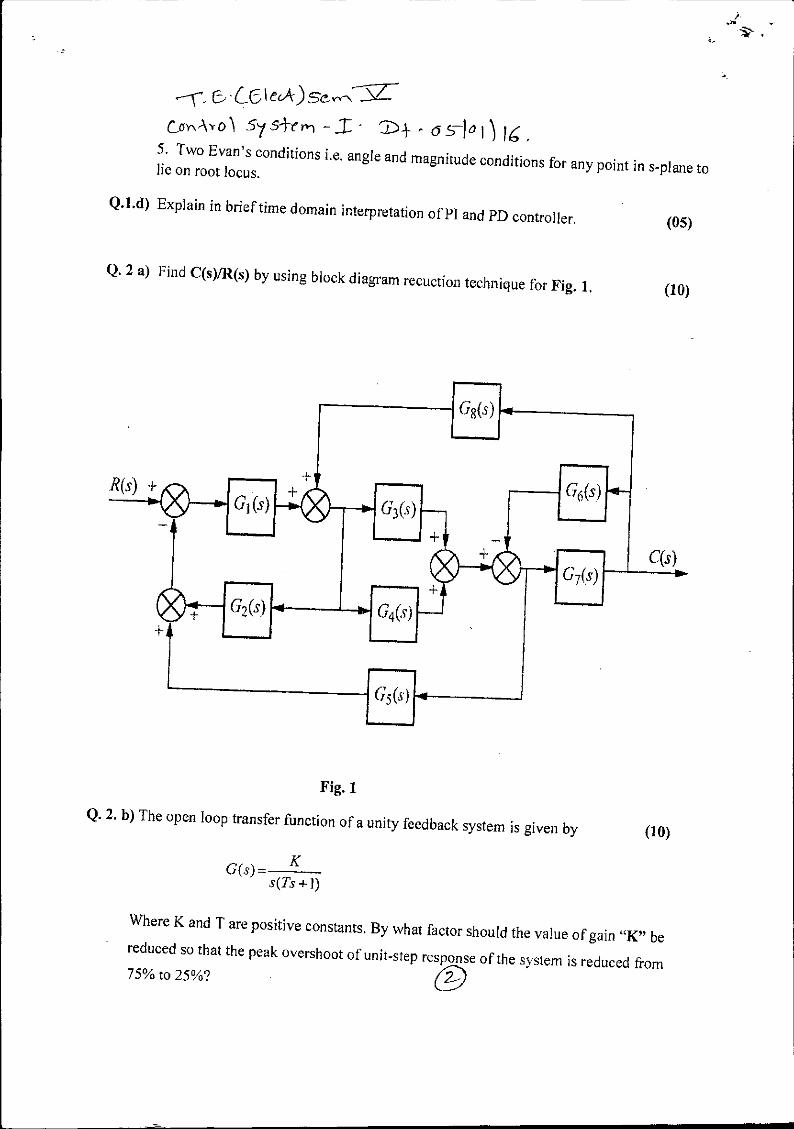
Q. 2 a) Find C(s)/12(s) by using block diagram recuction technique for Fig. 1. (10)
Fig. 1
Q. 2. b) The open loop transfer function of a unity feedback system is given by (10)
G(s)=
s(Ts
Where K and T are positive constants. By what factor should the value of gain "K" be
reduced so that the peak overshoot of unit-step response of the system is reduced from 75% to 25%?

c6iec,0 seincu— control sysiern -T rD4- 031 )) IC .
Q.3. a) (1)Using Routh criterion determine the relation between K and T so that unity feedback control system whose open loop transfer function given below is stable
G(s)=
s [s (s +10+ 71 (6)
(2)Determine the modified relation between K and T if all the roots of characteristics
equation as determined in (1) are to lie to the left of the line s = —1 in s-plane. (10)
Q.3. b) Unit step response of the first order unity feedback system is given by
100
Determine its (4)
a. Open loop transfer function.
b. Closed loop transfer function.
c. Steady state error for step input.
d. Steady state error for ramp input.
Q.4. a) Prove the following statement (10)
"The asymptotes cross the real axis at a point known as centroid, determined by the relationship: (sum of real parts of pole — sum of real parts of zeros)/ (number of poles — number of zeros)".
Q4 b) Consider the armature controlled cl.c. motor shown in Fig.2 . In this system ,
Rf - Resistance of Field winding (ohm) Lf inductance of Field winding (H) ia armature current (A) if Field current (A) ea applied armature voltage (V) eb back emf(V) TM torque developed by motor (Nm) 0 angular displacement of motor-shaft (rad) J equibvlaent moment of inertia of motor and load referred to motor shaft

ccil) Se rn -r sy1 /45 - r I T±- 0 3-10 1 . coy. s-lro
(kg-m2) fo equivalent viscous friction coefficent of motor and load referred to motor
shaft.
_V
Fig.2 Field Controlled D.C. Motor.
Derive the transfer function G(s) = 0(s)/E1(s) and also draw the complete block diagram for the
same. (10)
Q5 a) Obtain the transfer function in the given SFG in Fig. 3. (10)
Fig. 3

6- CE I et4 ) Yn JZ- ohNtrip) sys4e, _E --D . 051 to 1116
Q5 b) Consider the unity feedback system with (10)
G(s)=
(s + 3)(s+ 5) Show that the system cannot operate with a settling time of 2/3 second and a percentage overshoot of 1.5% with simple gain adjustment.
Q. 6) A unity feedback system with forward transfer function
G(s)=
(s + 2)(s+ 3)(s+ 7)
is operating with 10% overshoot.
a. What is the value of the appropriate static error constant?
b. Find the transfer function of a lag network so that the appropriate static error constant
equals 4 without appreciably changing the dominant poles of the uncompensated system
(20) Q.7) For the unity feedback system with
G(s)=
(s + 1)(s+ 4)
Design a P1D controller that will yield a peak time of 1.047 seconds and a damping ratio of 0.8, with zero error for step input.
(20)


y s3 eitA ,( CI )S-e,
evk c Mctc1'a JL
Bharatiya Vidya Bhavan's
Sardar Patel College of Engineering (A Government Aided Autonomous Institute)
Munshi Nagar, Andheri (West), Mumbai —400058.
Re-Examination January- 2016
Librattezrj.
cHic
Max. Marks: 100 Class: TX. B.Tech Semester: V Name of the Course: Electrical machines-II Instructions: I. Question No 1 is compulsory. 2. Attempt any four questions out of remaining six. 3. Draw neat diagrams 4. Assume suitable data if necessary and justify the same.
Duration: 3 Hour Program: B. Tech Course Code : EE 303
ril4s1-cr ch i C .
1 Ques. No
Max. Marks
Ql. (a) What is the need of leading power factor operation of synchronous motor. 05
Lab) Explain in brief the armature reaction in case of synchronous generator. 05
(c) "Explain how to make single phase Induction Motor as self start motor. 05
(d) What is synchronization. What are the conditions for synchronization. 05
Q2(a) An 11 kV, 50 Hz, 14860 kVA, three phase, 40 pole star connected hydroelectric generator gave the following data on open circuit.
20
I If in A , 10 15 1 20.5 25 1 30 ! 35 ' 40 I Ef in kV 1 6.45 9.0 1 11.0 12.2 1 13.25 I 14.0 1 14.5
S.C. Test: If =18 A, I„ =780 A
Z.P.F. Test: 11 =52.5 A, Ia =780 A, Vt =11 kV -- -0-.8—pf Fluff tire-Voltage regulation at laterirmature curieriTinn al fag
by i) MMF method and ii) ZPF method (take armature resistance of 0.2 ohms/phase)
Q3(a) What is the need of parallel operation of synchronous generator? What are the conditions to be satisfied for connecting two generators in parallel? What is the way of changing the load shared between the two generators?
03+03+02
(b) Two similar alternators operating in parallel have the following data: Alternator 1 — Capacity 2 MW, frequency drops from 50 Hz at no load to
48.0 Hz at full load Alternator 2 — Capacity 2 MW, frequency drops from 50.5 Hz at no load
to 48.5 Hz at full load. Prime mover speed regulation is linear.
(i) Calculate how a total load of 3.6 MW is shared by each alternator. Also find the operating bus frequency at this load.
(ii) Compute the maximum load that these two units can deliver
12

Teci, .C\ C) Se
El eciori tca VlisktkirveS - Og kill I • without overloading either of them.
Q4(a) Explain the slip test to calculate the reactances of salient pole synchronous j 10 machine.
(b) A 3300 V, star connected synchronous motor is operating at constant terminal I 10 voltage and constant excitation. Its synchronous impedance is (0.8-,j5)12. It operates at a power factor of 0.8 leading when drawing 800 kW from the mains. Find its power factor when the input is increased to 1200 kW, excitation remaining constant.
Q5(a) Explain the Blondel's model used for the analysis of salient pole 08 synchronous machines.
, (b) Draw and explain in brief the V-curves and inverted V- curves of i 08
synchronous motor.
(c) A synchronous generator supplying isolated load with constant field current. 04 Mechanical input to synchronous generator is increased; explain the effect on excitation voltage, armature voltage, armature current and power factor.
_ Q6(a) What are the advantages of field winding is on rotor and armature winding is 08
on stator in case of synchronous generator
(b) A 600 V, 6-pole , 3-phase, 50 Hz, star connected synchronous motor has a 1 12 resistance and synchronous reactance of 0.4 Q and 7 12 respectively. It takes a current of 15 A at upf when operating with a certain field current. With the field current remaining constant, the load torque is increased until the motor draws a current of 50 A. Find the torque (gross) developed and the new power factor.
Q7(a) Explain the procedure to draw the potier triangle in case of ZPF method. 08
(b) Draw the phasor diagrams of salient pole synchronous generator at leading, lagging and unity power factor. Do not neglect armature resistance.
06
(c) Discuss in brief the location and purpose of damper winding in synchronous machine.
06