Embed Size (px)
Citation preview

Santa Clara Valley Chapter, CPMT Societywww.cpmt.org/scv/
February 8, 2006
Page 1
ELECTRONICS MANUFACTURING SERVICES
© 2006 Sanmina-SCI Corporation. Sanmina-SCI is a trademark of Sanmina-SCI Corporation. All trademarks and registered trademarks are the property of their respective owners.
Impedance Characterization and Design Optimization of PCB Embedded Passive ComponentsPresented at the Feb. 8 2006 meeting, Santa Clara Valley Chapter, CPMT Society – www.cpmt.org/scv/
Nick Biunno and Franz GisinSanmina-SCI, CorpSan Jose, CA
Embedded Resistor Technology Drivers
High density component packages
Form factor reduction
Faster signal speed
Improved Signal Integrity noise margins
Weight reduction

Santa Clara Valley Chapter, CPMT Societywww.cpmt.org/scv/
February 8, 2006
Page 2
Embedded Passives Now All About Infrastructure
• CAD/CAM Design Support (what to embedded?)
• Cost Modeling
• Design Input and Design Rules
• Embedded Component Impedance Characterization
• Signal Integrity and Component Simulation
• NPI Proto-Typing and Volume Manufacturing
• Test and Reliability
• Standards
Future
Embedded Passive Technology Portfolio
C Capacitor L Inductor (Planar Magnetics)R Resistor
Embedded Passives
Discrete Networks DistributedBuried Capacitance®
C LR R C RCPower Distribution
NetworksDigital and AnalogApplications Low, High & Band Pass Filters
Resistive Networks

Santa Clara Valley Chapter, CPMT Societywww.cpmt.org/scv/
February 8, 2006
Page 3
Resistor Analysis for Embedded Conversion
Value Total Power Surface Embed Circuit Resistor Buried Buried Sheet(ohms) Qty. (watts) Tolerance Style Priority Tolerance Application Configuration Layer Quantity Resistance
20 60 0.063 1% 0402 ?? s R A 6033 9 0.063 5% 0402 s R A 933 3 0.063 5% 0603 s R A 3
33.2 31 0.100 1% RM0705 s R A 3175 81 0.063 1% 0402 s R A 81
Total 184
1K 30 5% 16 pin QSOP gnd(D) A B 301K 56 0.100 1% RM0705 gnd(D) A B 562K 6 0.100 1% RM0705 gnd(D) R B 6
4.75K 1 0.100 1% RM0705 gnd(D) R B 14.7K 15 5% 16 pin QSOP gnd(D) R B 15
Total 108
1K 2 0.063 5% 0402 2.5 V C11K 1 0.100 1% RM0705 2.5 V C12K 50 5% 16 pin QSOP 2.5 V C12K 4 0.100 1% RM0705 2.5 V C1
3.3K 0.063 5% 0603 2.5 V C13.32K 0.100 1% RM0705 2.5 V C14.75K 0.100 1% RM0705 2.5 V C14.7K 5% 16 pin QSOP 2.5 V C110K 4 0.063 5% 0603 2.5 V C110K 12 0.100 1% RM0705 2.5 V C1
1K 0.063 5% 0402 3.3 V C21K 12 0.100 1% RM0705 3.3 V C22K 5% 16 pin QSOP 3.3 V C22K 17 0.100 1% RM0705 3.3 V C2
3.3K 0.063 5% 0603 3.3 V C23.32K 0.100 1% RM0705 3.3 V C24.75K 20 0.100 1% RM0705 3.3 V A C2 204.7K 45 5% 16 pin QSOP 3.3 V A C2 4510K 1 0.063 5% 0603 3.3 V C210K 52 0.100 1% RM0705 3.3 V C2
1K 0.063 5% 0402 5.0 V C31K 9 0.100 1% RM0705 5.0 V C32K 5% 16 pin QSOP 5.0 V C32K 0.100 1% RM0705 5.0 V C3
3.3K 96 0.063 5% 0603 5.0 V A C3 963.32K 5 0.100 1% RM0705 5.0 V A C3 54.75K 0.100 1% RM0705 5.0 V C34.7K 15 5% 16 pin QSOP 5.0 V A C3 1510K 0.063 5% 0603 5.0 V C310K 22 0.100 1% RM0705 5.0 V C3
Total 659 Total 181
Basic Circuit Design Buried R-EP Design
25-50 ohms-sq.
50K ohm-sq.
50K ohm-sq.
10K ohm- sq.
50K ohm-sq.
Buried Capacitance® Drivers
Decreased Plane Inductances & Improves Broad Band Impedance
Reduced Size or Increased Functionality at Same Size
Lower Assembly Costs & Higher Reliability
Fewer Components = Less Solder Joints
Active Component
Gnd
PwrI & Z C
No BC™
Active Device
Decoupling Capacitors
Active Device
Decoupling Capacitors
With BC™

Santa Clara Valley Chapter, CPMT Societywww.cpmt.org/scv/
February 8, 2006
Page 4
Buried Capacitance® Product Family
Plane C
apac
itance
pf/in2
(pf/cm
2 )
BC12, BC16, BC8, BC16T, BC12T are all trademarks of Oak Mitsui TechnologiesHK-04 is a trademark of DuPont Electronic Materials
1000 (155) BC24™ & ZBC1000™1.0 mil (25µ)1600 (233) BC16™0.6 mil (16 µ)
1900 (310) BC12™0.5 mil (12 µ)
3100 (481) BC8™0.3 mil (8 µ)
11,000 (1,705) BC16T™0.6 mil (16 µ)
500 (78) ZBC2000®2.0 mil (50µ)
4500 (698) BC12TM™0.5 mil (12 µ)
800 (124) HK-04™1.0 mil (25µ)
Unsupported Laminate Material Characteristics
Property Units BC24 BC16 BC12 BC8* BC16T* BC12TM*
HK-04
Dielectric Thickness (µ)
Nominal 24 16 12 8 16 12 25
Peel Strength lbs/in 8 8 8 8 6 4 9.0
Dielectric Strength
KV/mil 5.3 7.3 5 5 2.8 6.2 6-7
Tensile Strength
Mpa (kpsi)
152 (22.0)
164 (23.8)
194 (28.2)
126 (18.3)
NA 110 (16.0)
>345 (>50)
Elongation % 18.5 16.5 11.5 8.5 NA 6.0 >50
Hi-Pot Test DC Volts 500 500 500 500 100 500 500
Thermal Shock
-35°C/125°C 400 Cycles
Pass Pass Pass TBD TBD TBD Pass: -65°C to 125°C- 100
Cycles Thermal
Stress (20Sec @ 288°C)
# Times >10 >10 >10 >10 >10 >10 Pass: 10 sec @ 288°C
Electro Migration
85C/85%RH, 35VDC
>1000 Hours
>1000 Hours
>1000 Hours
>1000 Hours
>1000 Hours >1000 Hours
1000 Hours @ 100VDC
Flammability Temp Rating
UL-94/ UL-746
V0 130°C
V0 130°C
V0 130°C
V0 130°C
Provisional V0 130°C
V0
Double sided core process Sequential Lamination
Double Sided Core Process

Santa Clara Valley Chapter, CPMT Societywww.cpmt.org/scv/
February 8, 2006
Page 5
Supported Laminate Material Characteristics
Property Condition Unit ZBC-2000® ZBC-1000™Dielectric Resin ---- ---- FR-4 FR-4 Dielectric Reinforcement ---- ---- e-glass e-glass
Hi-Pot Test DC Volts Volts (DC) 500 500
Electro-migration 85°C/85%
RH (DC Volts)
Hours @ (Volts) 2000 (50) 2000 (50)
Thermal Shock -35°C /
125°C 400 cycles
N/A Pass Pass
Peel Strength As received Ib/in2 >6.0 >6.0 Dielectric Breakdown 1 kV/sec Volts (DC) >2500 >2500
UL Rating ---- ---- 94-V0 94-V0 Bellcore/Telcordia Exception
TR-NWT-000078 N/A Granted In progress
BC™ Laminates Impedance
Capacitance increases as dielectric thickness decreasesNoise improves as the impedance is reduced
0.001
0.01
0.1
1
10
1 10 100 1000 10000
Frequency (MHz)
Self
Impe
danc
e (o
hms)
ZBC-2000
ZBC-1000
BC 24 micron
BC 16 micron
BC 8 micron
BC 12TM
BC 16T

Santa Clara Valley Chapter, CPMT Societywww.cpmt.org/scv/
February 8, 2006
Page 6
BC™ Laminate Inductive Impedance
Plane inductance is reduced as dielectric thickness decreases
Plane resonances are reduced as dielectric thickness decreases
0.0
0.1
0.2
0.3
0.4
0.5
0.6
0.7
0.8
0.9
1.0
0.0 0.5 1.0 1.5 2.0 2.5 3.0Frequency (GHz)
Self
Impe
danc
e (o
hms)
ZBC-2000ZBC-1000FaradFlex BC24FaradFlex BC16FaradFlex BC12TMFaradFlex BC8FaradFlex BC16T
Representative ZBC Design Examples(Plane Resonance Reduction)
W/O ZBC
With BC-24 With ZBC-2000® With BC-12TM
Santa Clara Valley Chapter, CPMT Societywww.cpmt.org/scv/
February 8, 2006
Page 7
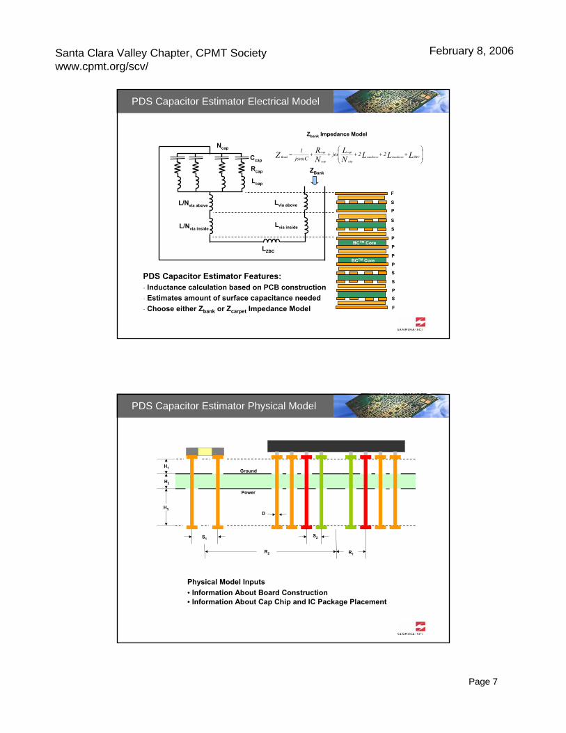
PDS Capacitor Estimator Electrical Model
PDS Capacitor Estimator Features:- Inductance calculation based on PCB construction- Estimates amount of surface capacitance needed- Choose either Zbank or Zcarpet Impedance Model
Lvia inside
Lvia above
LZBC
L/Nvia above
L/Nvia inside
Ccap
Rcap
Lcap
F
S
P
S
S
P
PBCTM Core
BCTM CoreP
P
P
S
S
S
F
⎟⎟
⎠
⎞
⎜⎜
⎝
⎛+++++= LLLN
LNRZ ZBCviaabovevaiabove
cap
cap
cap
capBank 22jω
jωωC1
Ncap
ZBank
Zbank Impedance Model
PDS Capacitor Estimator Physical Model
S2
Ground
Power
H1
D
H2
H3
S1
R2 R1
Physical Model Inputs• Information About Board Construction• Information About Cap Chip and IC Package Placement

Santa Clara Valley Chapter, CPMT Societywww.cpmt.org/scv/
February 8, 2006
Page 8
BCTMSpreading Inductance Calculation
Inductance Decreases as Plane Spacing Decreases
0
10
20
30
40
50
60
70
0.7 0.8 0.9 1.0 1.1 1.2 1.3 1.4
Radius IC to Cap Centers (in.)
"Spr
eadi
ng"
Indu
ctan
ce (p
H)
0.008
0.004
0.002
0.001
0.0005
Representative ZBC Design Examples(Capacitor Elimination)
Product# Caps Before # Caps After % Eliminated
ZBC 200048 17 64 %
BC 2448 13 72 %
BC 1648 12 74 %
BC 1248 11 75 %
BC 848 10 77 %
Based on 1156 Pin BGA Array, 3.3 V Power Distribution, 603 Style Bypass Caps

Santa Clara Valley Chapter, CPMT Societywww.cpmt.org/scv/
February 8, 2006
Page 9
Capacitive Coupling Test Board
Capacitive Dielectric8 micron FaradFlex BC8TM
Other Dielectrics In Test- FaradFlex BC12TM- Screen Printed PTF
Capacitor Dimensions1) .020” x .020”2) .040” x .040”3) .080” x .080”4) .160” x .160”5) .020” x .040”6) .080” x .040”7) .160” x .040”8) .320” x .040”9) .040” x .020”
10) .040” x .080”11) .040” x .160”12) .040” x .320”13) .020” x .020”14) .080” x .080”15) .160” x .160”16) .320” x .320”17) .080” x .080” ½ stub18) .080” x .080” 2x stub19) .160” x .160” 3x stub20) .160” x .160” 4x stub
2.000”50 ohm
.006”
Measurement Setup
Bit Pattern Test for Circuits 1-4 Pattern a
.020” x .020”
.040” x .040”
.080” x .080”
.160” x .160”

Santa Clara Valley Chapter, CPMT Societywww.cpmt.org/scv/
February 8, 2006
Page 10
Bit Pattern Test for Circuits 3,17,18 Pattern a
.080” x .080” ½ Stub
.080” x .080”
.080” x .080” 2x Stub
Bit Pattern Test for Circuit 12 Pattern (a) & (b)
.040” x .320” Capacitor Bit Pattern (b)
.040” x .320” Capacitor Bit Pattern (a)

Santa Clara Valley Chapter, CPMT Societywww.cpmt.org/scv/
February 8, 2006
Page 11
Eye Diagrams for Circuit 12 Pattern (a) & (b)
3.125 Gb/s 6.25 Gb/s 12.5 Gb/s
3.125 Gb/s 6.25 Gb/s 12.5 Gb/s
25 Bit Pattern (a)
25 Bit Pattern (b)
Resistor Impedance Measure Test Board
Two Objectives of Resistor Impedance Measurements are;1. Characterize by Geometry2. Characterize by Board Construction and Application
1 2 3
45
6
Sheet Resistance = 100 ohm-sq.
PTF Film Thickness = 0.007”
Rectangular Resistor Parameters
210.040”.120”6 -
140.040”.080”5 -
70.040”.040”4 -
420.020”.120”3 -
290.020”.080”2 -
160.020”.040”1 -OhmsWidthLength
Annular Resistor Parameters
Sheet Resistance = 1000 ohm-sq.
PTF Film Thickness = 0.007”
70.035”.045”Ohms
Inner Diameter
Outer Diameter

Santa Clara Valley Chapter, CPMT Societywww.cpmt.org/scv/
February 8, 2006
Page 12
PTF Resistor Design
B
L
B
L
RR
ttRRR ⎟
⎠
⎞⎜⎝
⎛=×= ρρ
B
L
S RRRR= NRR S×=or
ρ = Resistivity (ohm-unit length)t = Resistor film thickness RL = Length in direction of current flowRB = WidthRs = Sheet resistance (Ω/ ) N = The number of series squares
⎟⎟⎠
⎞⎜⎜⎝
⎛=DD
tR1
2ln2πρ
R = Resistor value (ohms)ρ = Resistivity (ohm-unit length)t = Resistor average thickness D1 = Resistor inner pad diameterD2 = Resistor outer ring diameter
RL
RB
Ohms
Ohms
D1
D2
D1
D2
Z(resistive) Measurement Set Up
Port Connections to the Annular Resistor are Asymmetric
Port 1 Port 2
Port 1 Port 2
.032”
Measurement Setup for AnnualrAnd Rectangular Resistors
Port Connections to Rectangular Resistors

Santa Clara Valley Chapter, CPMT Societywww.cpmt.org/scv/
February 8, 2006
Page 13
S21 Measurements for Rectangular Resistors
• Impedance Predictable to 7 GHz• Z Response Above 7 GHz Not Well Understood
-35
-30
-25
-20
-15
-10
-5
0
1 3 5 7 9 11 13 15
Frequency (GHz)
Loss
(dB
)
(4) 70 ohms (5) 140 ohms (6) 210 ohms (3) 420 ohms
S21 Measurement for Annular Geometry
• Impedance Predictable to 7 GHz• Z Response Above 7 GHz Not Well Understood
-40
-35
-30
-25
-20
-15
-10
-5
0
5
1 2 3 4 5 6 7 8
Frequency (GHz)
Loss
(dB
)
Rectangular 70 Ohms
Annular 70 Ohms

Santa Clara Valley Chapter, CPMT Societywww.cpmt.org/scv/
February 8, 2006
Page 14
Design Options Showing Rectangular & Annular Designs
Design Options for Array Resistor Patterns
RectangularPattern
AnnularPattern
Annular Design – Inner Layer
Power Plane Layer with 95 3.3K ohm Pull-up Resistors
Before
After

Santa Clara Valley Chapter, CPMT Societywww.cpmt.org/scv/
February 8, 2006
Page 15
Annular Design Surface Area Gain
Gained Surface Area ~ 38% of Area Shown
Before Design Conversion
After Design Conversion
Mentor Graphics Supermax CAD Software
(Provided by Mentor Graphics)
Hierarchical Rules: design level, by component, by net or net class, by pin or pad stack, by layer, between layers
The Supermax technology provides an effective platform for design of embedded passive components – resistors, capacitors, inductors and transformers

Santa Clara Valley Chapter, CPMT Societywww.cpmt.org/scv/
February 8, 2006
Page 16
Conclusion (What we are doing this year)
• Work in Progress to Support CAD/CAM Design
• Continue Work on Component Impedance Measurements
Develop New Test Structures and Methods of Measurement Extraction
Increase Range of Resistor Values to Cover Several Decades
Design Test Structures for Combined Passive (RC, RL and RCL) Elements
• Confirm Impedance Measurements with Component Simulation Modeling
Thank YouThank You


![Color Panel Memory Test [CPMT]](https://img.dokumen.tips/doc/110x75/549ab475b4795938098b4593/color-panel-memory-test-cpmt.jpg)