Embed Size (px)
Citation preview
©2017 by System Plus Consulting | Samsung LM101A 1
21 rue la Noue Bras de Fer44200 NANTES - FRANCE +33 2 40 18 09 16 [email protected] www.systemplus.fr
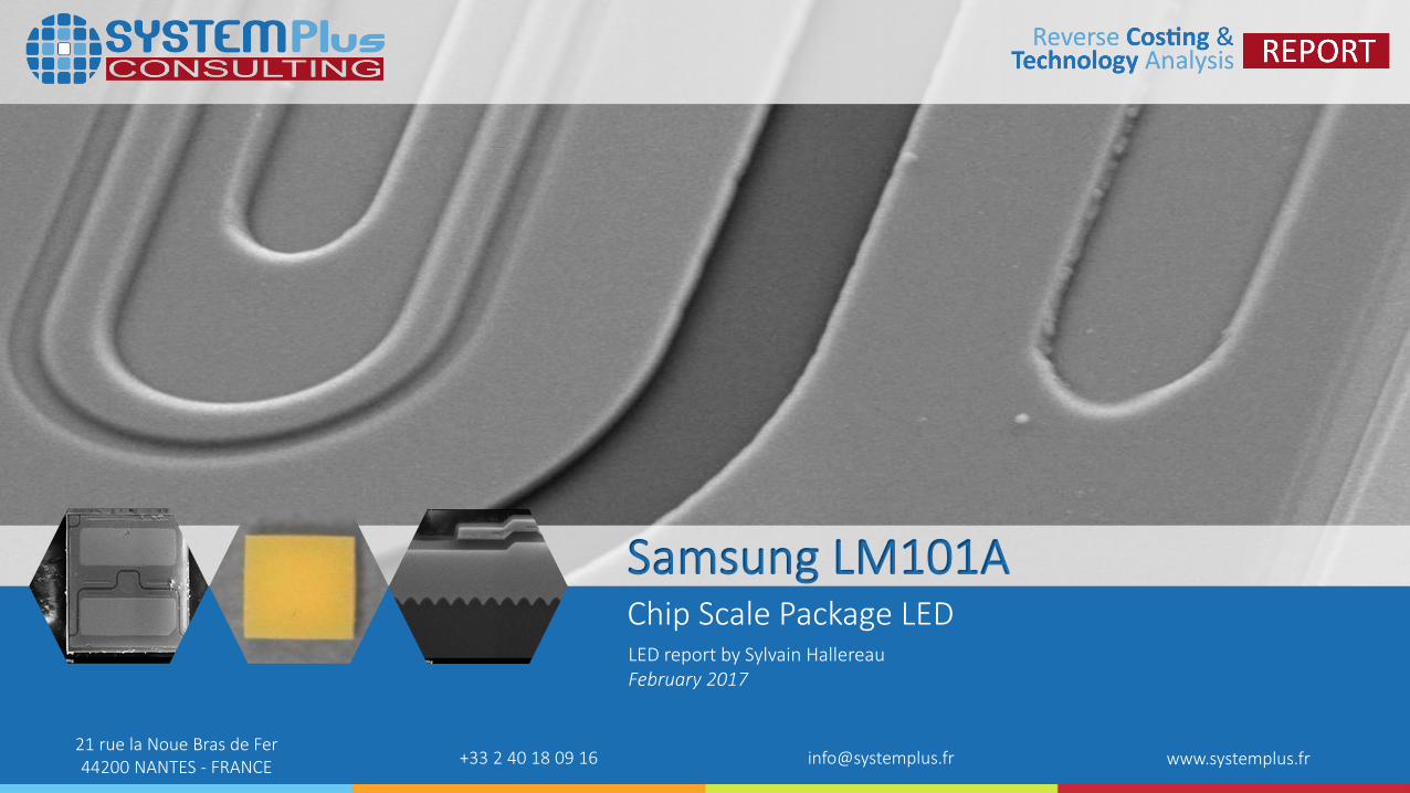
Samsung LM101A Chip Scale Package LEDLED report by Sylvain HallereauFebruary 2017

©2017 by System Plus Consulting | Samsung LM101A 2
SUMMARY
Overview / Introduction 3
o Executive Summary
o Reverse Costing Methodology
Company Profile 10
o Samsung
Physical Analysis 15
o Synthesis of the Physical Analysis
o Package analysis
Package Views & Dimensions
Package Cross-Section
o LED Die
LED Die View & Dimensions
LED Die Process
LED Die Cross-Section
LED Die Cross-Section Cathode
LED Die Cross-Section Anode
LED Die Process Characteristic
LED Manufacturing Process 41
o LED Die Front-End Process Flow
o LED Die Fabrication Unit
o Package Process flow
o Final Test & Packaging Fabrication unit
Cost Analysis 51
o Synthesis of the cost analysis
o Yields Explanation & Hypotheses
o LED die
LED Front-End Cost
LED Die Probe Test, Thinning & Dicing
LED Wafer Cost
LED Die Cost
o LED Component
Packaging Cost
Packaging Step Cost
Component Cost
Component Cost Evolution
Price Analysis 65
o Estimation of selling price
Company services 68

©2017 by System Plus Consulting | Samsung LM101A 3
Overview / Introductiono Executive Summaryo Reverse Costing
Methodology
Company Profile & SupplyChain
Physical Analysis
Manufacturing Process Flow
Cost Analysis
Selling Price Analysis
About System Plus
Executive Summary
This full reverse costing study has been conducted to provide insight on technology data, manufacturing cost and selling price of theSamsung LM101A Chip Scale Package LED.
The SCP8TT78HPL1TLS06E is the first generation Chip Scale Package (CSP) LED device from Samsung. The LED presents a flip chipstructure.
The SCP8TT78HPL1TLS06E is a neutral white (4000°K) LED with a CRI of 80.
The design allows low thermal resistance and a high degree of reliability with plastic free structure.
The wafer level packaging makes a very competitive cost.
The report goes into depth in its analysis of the packaging and the components, with images of the new Chip scale package structure.
The LM101A LED family is adapted to Bulb, Candle, MR16, PAR, Spot light products. The SCP LED is a new market which represents 0.8%of the LED market today but will be 6 times larger in 2021, (yole develloppement). With this component, Samsung positions in on thisnew CSP LED market.

©2017 by System Plus Consulting | Samsung LM101A 4
Overview / Introduction
Company Profile & SupplyChain
Physical Analysiso Synthesiso Packageo Die designo Die Cross-Section
Manufacturing Process Flow
Cost Analysis
Selling Price Analysis
About System Plus
Package Views & Dimensions
o The package type is a chip scale package (CSP)
o Package size : 1.2mm x 1.2mm x 0.4mm
o Package area: 1.44mm²
o LED area: 0.67mm² (47% of the package)
Package Front view Package Back view
Package Side view
0.4mm
0.3
6m
m
0.82mm
0.82mm
1.2mm
0.2mm 0.2mm
©2017 by System Plus Consulting | Samsung LM101A 5
Overview / Introduction
Company Profile & SupplyChain
Physical Analysiso Synthesiso Packageo Die designo Die Cross-Section
Manufacturing Process Flow
Cost Analysis
Selling Price Analysis
About System Plus
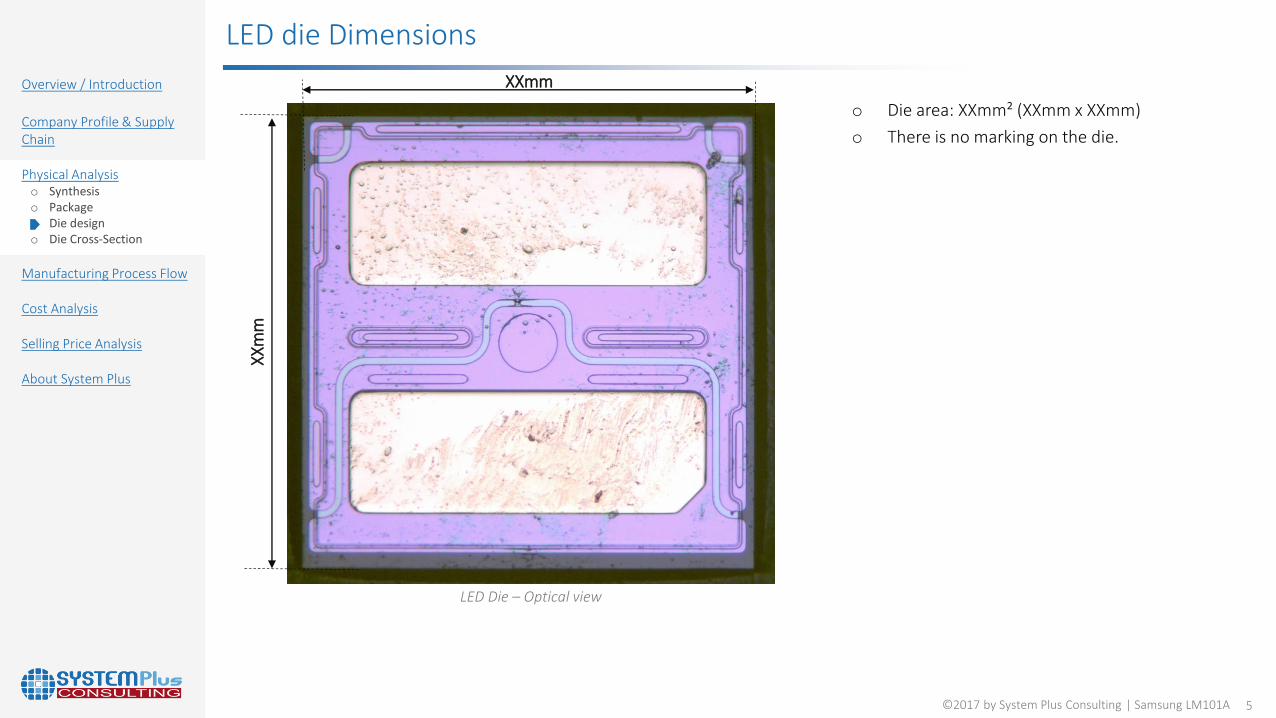
LED die Dimensions
LED Die – Optical view
XXm
m
o Die area: XXmm² (XXmm x XXmm)
o There is no marking on the die.
XXmm

©2017 by System Plus Consulting | Samsung LM101A 6
Overview / Introduction
Company Profile & SupplyChain
Physical Analysiso Synthesiso Packageo Die designo Die Cross-Section
Manufacturing Process Flow
Cost Analysis
Selling Price Analysis
About System Plus
Die process
Detail back side – SEM View

©2017 by System Plus Consulting | Samsung LM101A 7
Overview / Introduction
Company Profile & SupplyChain
Physical Analysiso Synthesiso Packageo Die designo Die Cross-Section
Manufacturing Process Flow
Cost Analysis
Selling Price Analysis
About System Plus
Die cross section – Cathode Electrode EDX
Cathode metal layers – EDX Epitaxy

©2017 by System Plus Consulting | Samsung LM101A 8
Overview / Introduction
Company Profile & SupplyChain
Physical Analysis
Manufacturing Process Flowo LED Front-End Fab Unito LED Front-End Processo Packaging Processo Packaging Unit
Cost Analysis
Selling Price Analysis
About System Plus
LED Process Flow (1/2)
Epitaxy
•Epitaxy GaN
Anode
Insulation
GaN Epitaxy
PSS (Patterned Sapphire Substrate)
Drawing not to Scale

©2017 by System Plus Consulting | Samsung LM101A 9
Overview / Introduction
Company Profile & SupplyChain
Physical Analysis
Manufacturing Process Flow
Cost Analysiso Synthesiso Die Costo Packaging Costo Component Costo Cost Evolution
Selling Price Analysis
About System Plus
LED Front-End Cost

©2017 by System Plus Consulting | Samsung LM101A 10
Overview / Introduction
Company Profile & SupplyChain
Physical Analysis
Manufacturing Process Flow
Cost Analysiso Synthesiso Die Costo Packaging Costo Component Costo Cost Evolution
Selling Price Analysis
About System Plus
LED Wafer Cost per process steps

©2017 by System Plus Consulting | Samsung LM101A 11
Overview / Introduction
Company Profile & SupplyChain
Physical Analysis
Manufacturing Process Flow
Cost Analysiso Synthesiso Die Costo Packaging Costo Component Costo Cost Evolution
Selling Price Analysis
About System Plus
Component Cost

©2017 by System Plus Consulting | Samsung LM101A 12
COMPANYSERVICES

©2017 by System Plus Consulting | Samsung LM101A 13
Overview / Introduction
Company Profile & SupplyChain
Physical Analysis
Manufacturing Process Flow
Cost Analysis
Selling Price Analysis
About System Pluso Company serviceso Related reportso Feedbackso Contacto Legal
Business Models Fields of Expertise
Custom Analyses(>130 analyses per year)
Reports(>40 reports per year)
Costing Tools
Trainings

©2017 by System Plus Consulting | Samsung LM101A 14
Overview / Introduction
Company Profile & SupplyChain
Physical Analysis
Manufacturing Process Flow
Cost Analysis
Selling Price Analysis
About System Pluso Company serviceso Related reportso Feedbackso Contacto Legal
MARKET AND TECHNOLOGY REPORTS - YOLE DÉVELOPPEMENT
LED• CSP LED Lighting module 2017 • MicroLED Displays 2017 • LED Packaging 2017 • Automotive Lighting 2016• Bulk GaN Substrate Market 2017
PATENT ANALYSIS - KNOWMADE
REVERSE COSTING ANALYSES - SYSTEM PLUS CONSULTING
LED• SP16273 - SETi 2 UVC 270 LED• SP15224 - Toshiba TL1L4 GaN on Si LED• SP13129 - SORAA GaN on GaN LED
Related Reports

©2017 by System Plus Consulting | Samsung LM101A 15
Overview / Introduction
Company Profile & SupplyChain
Physical Analysis
Manufacturing Process Flow
Cost Analysis
Selling Price Analysis
About System Pluso Company serviceso Related reportso Feedbackso Contacto Legal
Contact
Headquarters21 rue La Noue Bras de Fer44200 NantesFRANCE+33 2 40 18 09 [email protected]
Europe Sales OfficeLizzie LEVENEZFrankfurt am MainGERMANY+49 151 23 54 41 [email protected]
America Sales OfficeSteve [email protected]
www.systemplus.fr
Asia Sales OfficeTakashi [email protected]
Mavis WANGGREATER [email protected]
NANTESHeadquarter
FRANKFURT/MAINEuropa Sales Office
LYONYOLE HQ
TOKYOYOLE KK
GREATER CHINAYOLE
PHOENIXYOLE Inc.