Embed Size (px)
Citation preview

Elliot Briggs1, Chunmei Kang2,
Amit Mane2, Dan McLane2, Brian Nutter1
SDR’11 - WinnComm Europe
Brussels, Belgium June 22nd – 24th
Sample Clock Offset Detection and
Correction in the LTE Downlink Receiver
1: Texas Tech University, 2: Innovative Integration

Presentation Overview
• OFDM Receiver Synchronization Basics
• Mechanics of Sample Clock Offset
• Sample Clock Offset Detection
• Developed Sample Clock Correction Technique
• Results
1

OFDM Receiver Synchronization Basics
IDF
T
…
Para
llel to
Serial
…
D/A
Com
ple
x s
ym
bols
TX
Sample
clock
Add CP
~
Freq. offset
* WGN
channel A/D
RX
Sample
clock Serial to
Para
llel
Remove CP …
DF
T
Single/Multiple
path delay
…
Com
ple
x s
ym
bols
Signal Impairments
Traditional OFDM model example:
Impairments:
• AWGN: weak (noisy) signal
• Frequency shift: errors in RF electronics (TX and RX)
• Delay: Asynchronous startup time, multiple paths
• Sample Clock Offset?
2

-4 -3 -2 -1 0 1 2 3 4-0.4
-0.2
0
0.2
0.4
0.6
0.8
1
FFT bin center positions at the Receiver (subcarrier index)
Ideal Orthogonal Reception
OFDM Receiver Synchronization Basics
Ideal OFDM Reception:
•The receiver’s FFT bins are
aligned with each subcarrier
• Here, at the receiver, each
subcarrier is orthogonal to the
others
3

OFDM Receiver Synchronization Basics
-4 -3 -2 -1 0 1 2 3 4-0.4
-0.2
0
0.2
0.4
0.6
0.8
1
FFT bin center positions at the Receiver (subcarrier index)
Reception with ICI from 20% Frequency Shift
OFDM Reception Affected by
Frequency shift:
• Each FFT bin is misaligned by
an equal amount
• Each received subcarrier
experiences the same amount
of ICI
4

OFDM Receiver Synchronization Basics
-4 -3 -2 -1 0 1 2 3 4-0.4
-0.2
0
0.2
0.4
0.6
0.8
1
FFT bin center positions at the Receiver (subcarrier index)
Reception with ICI from 5% Sample Clock Offset
OFDM Reception Affected by
Sample Clock Offset:
• Each FFT bin has a
cumulative amount of shift
• The outer subcarrier positions
experience the most ICI
5

OFDM Receiver Synchronization Basics
0 256 512 768 1024 1280 1536 1792 20480
0.2
0.4
0.6
0.8
1
1.2
subcarrier index
norm
aliz
ed m
agnitude
LTE signal with 1,229 Hz sample clock offset at the receiver (40ppm total)
• 40 ppm error at the receiver
simulates the maximum error from 20
ppm clock oscillators at the
transmitter and receiver
• 40ppm = 1.229 kHz , 8.2% of one
subcarrier spacing
• Here, the SNR is 50 dB before the
sampling clock error is added
6

OFDM Receiver Synchronization Basics
-1 -0.8 -0.6 -0.4 -0.2 0 0.2 0.4 0.6 0.8 1-1
-0.8
-0.6
-0.4
-0.2
0
0.2
0.4
0.6
0.8
1
real
imagin
ary
LTE signal with 1,229 Hz sample clock offset at the receiver (40ppm total)
-1 -0.8 -0.6 -0.4 -0.2 0 0.2 0.4 0.6 0.8 1-1
-0.8
-0.6
-0.4
-0.2
0
0.2
0.4
0.6
0.8
1
realim
agin
ary
LTE signal with 1,229 Hz sample clock offset at the receiver (40ppm total)
• A slight phase shift occurs from
fractional timing offset
• The outer subcarrier positions
are no longer orthogonal and
contain energy from neighboring
subcarriers
• After the phase is unwound,
only the ICI component remains
• The ICI appears as noise at the
outer subcarrier locations
7
OFDM Receiver Synchronization Basics
1 200 400 600 800 1000 12000
2
4
6
8
10
12
14
16
18
subcarrier index
degra
dation (
dB
)
SNR Degradation vs. Subcarrier Index at Es/No = 50 dB
1 ppm
5 ppm
10 ppm
20 ppm
• ICI causes SNR degradation
which is the most severe at the
outer subcarrier locations.
• Even a 5ppm sample clock error
can cause 6 dB of degradation
when Es/No = 50 dB
2610 10
3
11log10 s
o
sn fn
N
ED
8
[1]

OFDM Receiver Synchronization Basics
5 10 15 20 25 30 35 40
10-1
100
101
102
clock offset (ppm)
degra
dation (
dB
)
SNR Degradation vs. SCO at Varying Es/No (subcarrier index = 1200)
20 dB
30 dB
40 dB
50 dB
• The level of degradation is
displayed for several levels of
SNR
• The SNR is adversely affected,
even with modest clock offsets
9

Mechanics of Sample Clock Offset
… …
time
symbol duration Cyclic prefix duration
LTE Example:
• “Extended” cyclic prefix mode
• 20 MHz mode
• Ideally, each symbol lasts only 83.33 μs
Transmitted OFDM symbols:
MHz72.301sT
512CPN
2048FFTN
μs33.83sFFTCPsymbol TNNT
CP CP CP
10
[2]
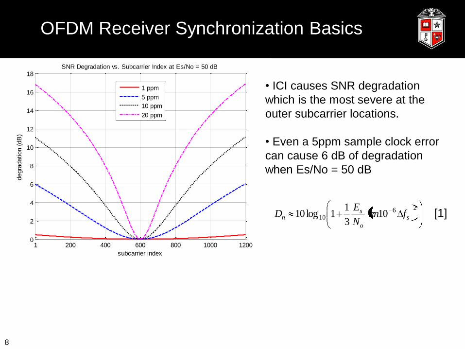
Mechanics of Sample Clock Offset
… …
sampled time
Received OFDM symbols:
perfect sample clock
frequency:
sample clock frequency
is too fast: … …
… … sample clock frequency
is too slow:
μs33.83sFFTCPsymbol TNNT
errors fT /1MHz72.301• 2560 samples will take a longer or shorter amount
of time for the receiver to collect, depending on the
offset conditions
• The rate that the symbols drift from the perfect
case directly indicates the sampling clock offset
magnitude.
• The direction in which the symbols drift indicate
the sampling clock offset direction
CP CP CP
CP CP CP
CP CP CP
11
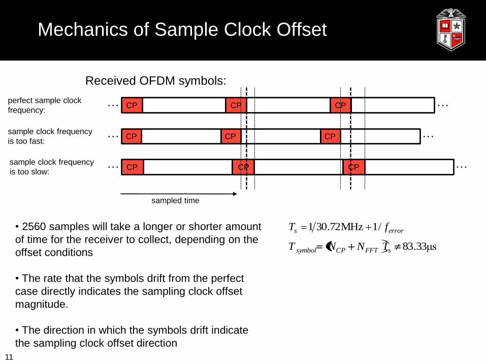
Sample Clock Offset Detection
Any DFT-based OFDM system must have an FFT window
timing synchronization component to properly align the
FFT window
… …
FFT window t-2 FFT window t-1 FFT window t
time
CP CP CP
Any FFT timing synchronization method can give sample clock offset information
• Using the LTE Primary Synchronization Signal (PSS)
o Timing information provided every 5 ms
• Cyclic Prefix Correlation
oTiming information provided every 83.33 μs
12

Sample Clock Offset Detection
Example: (-)+100 Hz clock offset error:
• Generates (removes) 100 extra samples per second.
• This will generate (remove) 1 sample for after 120 OFDM
symbols, or 0.0083 samples to each symbol
• A +12 kHz clock offset will generate an entire sample for
each OFDM symbol
N
t
offsetoffseterror tnStnSN
nf1
]1[][000,12
][
13

0 2 4 6 8 10 12 14
x 104
0
500
1000
1500
2000
2500
Symbol Start Location with Respect to the RX Clock (600 Hz SCO @ RX)
symbol index
sym
bol sta
rt s
am
ple
index
Sample Clock Offset Detection
Hz 60005.000,12]1[][000,12
][1
N
t
offsetoffseterror tnStnSN
nf
-2 -1 0 1 20
2
4
6
8
10
12x 10
4 timing drift distribution
symbol-to-symbol timing offset difference
frequency
000,135Nn
05.
14
0 5 10 15 20 25 30 35 400
0.1
0.2
0.3
0.4
0.5
0.6
0.7
0.8
0.9
1
OFDM Symbol Index
fractional dela
y (
fractional sam
ple
s)
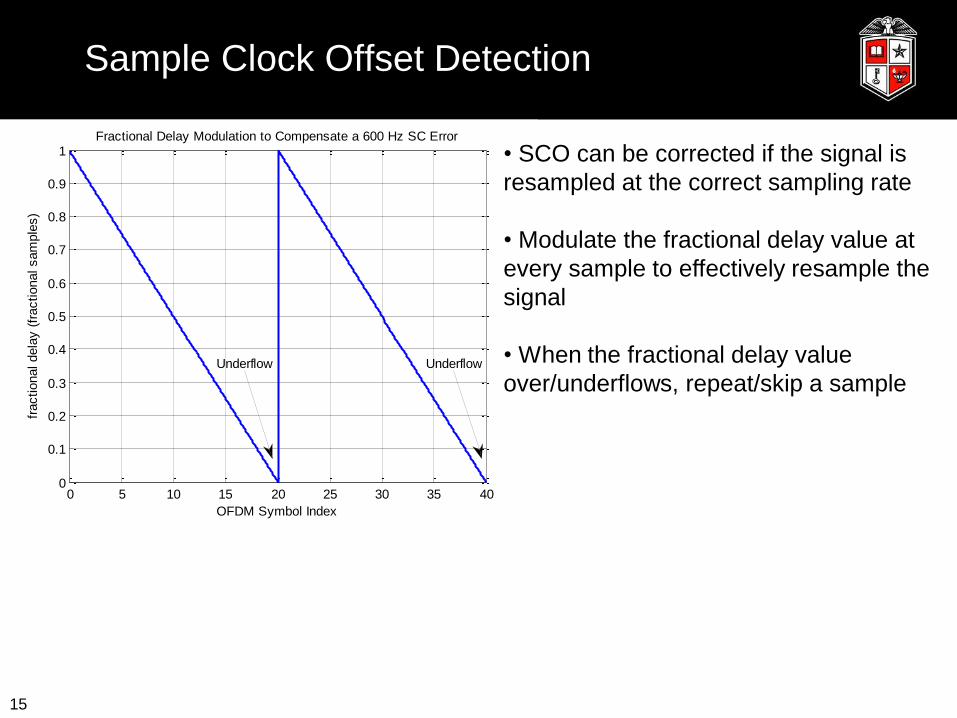
Fractional Delay Modulation to Compensate a 600 Hz SC Error
Underflow Underflow
• SCO can be corrected if the signal is
resampled at the correct sampling rate
• Modulate the fractional delay value at
every sample to effectively resample the
signal
• When the fractional delay value
over/underflows, repeat/skip a sample
Sample Clock Offset Detection
15

0 5 10 15 20 25 30 35 400
0.1
0.2
0.3
0.4
0.5
0.6
0.7
0.8
0.9
1
OFDM Symbol Index
fractional dela
y (
fractional sam
ple
s)
Fractional Delay Modulation to Compensate a 600 Hz SC Error
Underflow Underflow
• In this example, each sample has a
-.05/2560 delay difference from the
previous sample to correct the .05/2560
from the sample clock offset.
• When a negative delay is requested, a
sample is skipped.
• Here, fewer samples are produced at
the output of the resampling filter than
are input
• Ideally, the resampler produces 2560
samples per 83.33 μs
• The signal should have stationary
symbol timing after resampling
Developed Sample Clock Correction Technique
The resampler “compresses” the signal
by continuously reducing the delay for
each sample
1 16

Developed Sample Clock Correction Technique
• The ML timing and frequency offset estimator [3] uses the cyclic prefix
o The timing estimate is used by the loop filter and to trigger an FFT
conversion
o The frequency offset estimate is used to correct residual frequency shift
1 17

Developed Sample Clock Correction Technique
• The receiver uses feedback correction to adjust the symbol timing and
frequency correction
• The timing loop filter averages many timing estimates to get an average
window drift rate, just as in the previous example
• The delay accumulator constantly accumulates fractional delay and modulates
a fractional resampling filter
18

22 24 26 28 30 32 34 36 38 4016
18
20
22
24
26
28
30
32
34
36
38
40FPGA Hardware Results - 40 ppm SCO compensation performance
channel Es/No (dB)
measure
d e
ffective E
s/N
o (
dB
)
perfect reception, no SCO
40 ppm SCO, no compensation
40 ppm SCO, with compensation
• Design implemented in an
X5-400M FPGA board by
Innovative Integration
• Two separate clocks are
used, the frequency difference
is measured
• With SCO compensation
enabled, the minimum SNR
gain is around 3 dB
• SNR gains increase at higher
values of Es/No (~ 6 dB)!
FPGA Hardware Implementation Results
1 19
FPGA Hardware Implementation Results
22 24 26 28 30 32 34 36 38 405
10
15
20
25
30
35
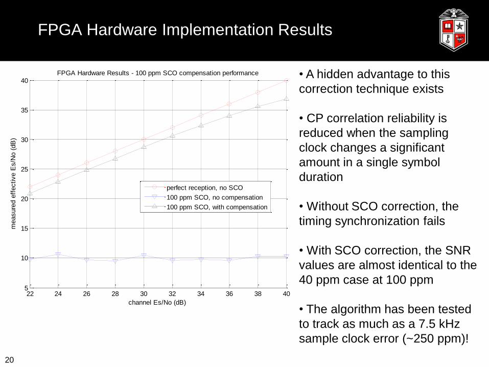
40FPGA Hardware Results - 100 ppm SCO compensation performance
channel Es/No (dB)
measure
d e
ffective E
s/N
o (
dB
)
perfect reception, no SCO
100 ppm SCO, no compensation
100 ppm SCO, with compensation
• A hidden advantage to this
correction technique exists
• CP correlation reliability is
reduced when the sampling
clock changes a significant
amount in a single symbol
duration
• Without SCO correction, the
timing synchronization fails
• With SCO correction, the SNR
values are almost identical to the
40 ppm case at 100 ppm
• The algorithm has been tested
to track as much as a 7.5 kHz
sample clock error (~250 ppm)!
20

FPGA Hardware Implementation Results
2 4 6 8 10 12 14 1610
-3
10-2
10-1
100
400M, 16QAM, SCO=0KHz, CFO=100KHz
Es/No
BE
R
measured BER
theoretical BER
• CFO = 100 kHz : frequency shift of over 13 subcarrier spacings
• SCO = 7.5 kHz : ~250 ppm sampling clock offset
3 4 5 6 7 8 9 1010
-4
10-3
10-2
10-1
100
400M, QPSK, SCO=7.5KHz, CFO=100KHz
Es/No
BE
R
measured BER
theoretical BER
21

FPGA Hardware Implementation Results
Corner Cases:
• Maintains timing lock down to 3dB SNR
• Maintains receivability:
o LTE cell ID decode, frame sync successful
SNR = 5dB
CFO = ±75 kHz (± 5 subcarrier spacings)
SCO = ±4 kHz (±133.33 ppm)
22

• The developed SCO measurement and correction method
allows the LTE user equipment to be equipped with a lower
cost, less precise sample clock source.
• Any timing synchronization algorithm can be employed to
generate sample clock offset measurements to be used for
correction
• The measurement and correction is in the time domain,
so the algorithm is agnostic to any frequency domain
information (reference symbols, training, etc).
• Can be applied to any OFDM-based standard
Conclusions
23

• May be useful for surveillance applications, maximizes
OFDM signal reception quality for any OFDM signal
Conclusions
24

References
[1] T. Pollet, P. Spruyt, and M. Moeneclaey, "The BER performance of OFDM systems using
non-synchronized sampling," Proceedings of the IEEE Global Telecommunications
Conference (GLOBECOM'94), San Francisco, USA, November 1994, pp. 253-257.
[2] 3GPP TS 36.211 V8.9.0 “Physical Channels and Modulation”. Rel. 8.
[3] J.J. van de Beek, M. Sandell, P.O. Börjesson, "ML Estimation of Time
and Frequency Offset in OFDM Systems," IEEE Transactions on Signal
Processing, Vol. 45, No. 7, July 1997, pp. 1800 - 1805.