Embed Size (px)
Citation preview
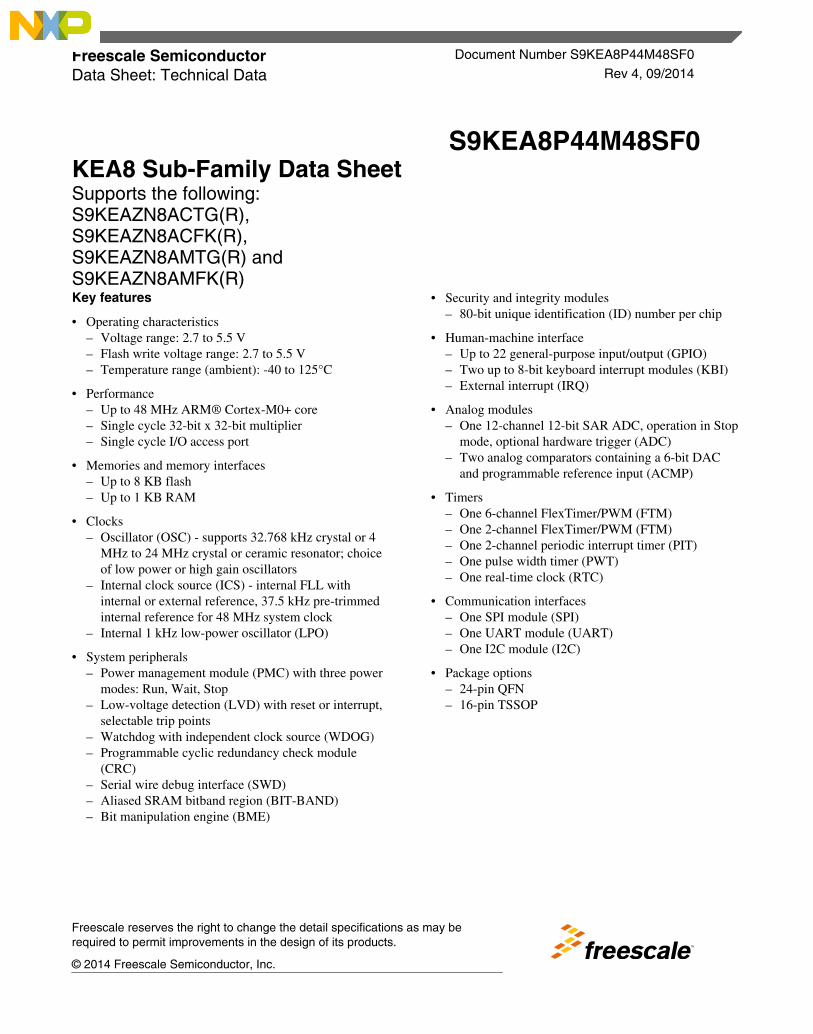
S9KEA8P44M48SF0KEA8 Sub-Family Data SheetSupports the following:S9KEAZN8ACTG(R),S9KEAZN8ACFK(R),S9KEAZN8AMTG(R) andS9KEAZN8AMFK(R)Key features
• Operating characteristics– Voltage range: 2.7 to 5.5 V– Flash write voltage range: 2.7 to 5.5 V– Temperature range (ambient): -40 to 125°C
• Performance– Up to 48 MHz ARM® Cortex-M0+ core– Single cycle 32-bit x 32-bit multiplier– Single cycle I/O access port
• Memories and memory interfaces– Up to 8 KB flash– Up to 1 KB RAM
• Clocks– Oscillator (OSC) - supports 32.768 kHz crystal or 4
MHz to 24 MHz crystal or ceramic resonator; choiceof low power or high gain oscillators
– Internal clock source (ICS) - internal FLL withinternal or external reference, 37.5 kHz pre-trimmedinternal reference for 48 MHz system clock
– Internal 1 kHz low-power oscillator (LPO)
• System peripherals– Power management module (PMC) with three power
modes: Run, Wait, Stop– Low-voltage detection (LVD) with reset or interrupt,
selectable trip points– Watchdog with independent clock source (WDOG)– Programmable cyclic redundancy check module
(CRC)– Serial wire debug interface (SWD)– Aliased SRAM bitband region (BIT-BAND)– Bit manipulation engine (BME)
• Security and integrity modules– 80-bit unique identification (ID) number per chip
• Human-machine interface– Up to 22 general-purpose input/output (GPIO)– Two up to 8-bit keyboard interrupt modules (KBI)– External interrupt (IRQ)
• Analog modules– One 12-channel 12-bit SAR ADC, operation in Stop
mode, optional hardware trigger (ADC)– Two analog comparators containing a 6-bit DAC
and programmable reference input (ACMP)
• Timers– One 6-channel FlexTimer/PWM (FTM)– One 2-channel FlexTimer/PWM (FTM)– One 2-channel periodic interrupt timer (PIT)– One pulse width timer (PWT)– One real-time clock (RTC)
• Communication interfaces– One SPI module (SPI)– One UART module (UART)– One I2C module (I2C)
• Package options– 24-pin QFN– 16-pin TSSOP
Freescale Semiconductor Document Number S9KEA8P44M48SF0
Data Sheet: Technical Data Rev 4, 09/2014
Freescale reserves the right to change the detail specifications as may berequired to permit improvements in the design of its products.
© 2014 Freescale Semiconductor, Inc.
Table of Contents1 Ordering parts.......................................................................................3
1.1 Determining valid orderable parts............................................... 3
2 Part identification................................................................................. 3
2.1 Description...................................................................................3
2.2 Format..........................................................................................3
2.3 Fields............................................................................................3
2.4 Example....................................................................................... 4
3 Ratings..................................................................................................4
3.1 Thermal handling ratings............................................................. 4
3.2 Moisture handling ratings............................................................ 4
3.3 ESD handling ratings................................................................... 5
3.4 Voltage and current operating ratings..........................................5
4 General................................................................................................. 6
4.1 Nonswitching electrical specifications........................................ 6
4.1.1 DC characteristics.......................................................... 6
4.1.2 Supply current characteristics........................................ 12
4.1.3 EMC performance..........................................................14
4.2 Switching specifications.............................................................. 14
4.2.1 Control timing................................................................ 14
4.2.2 FTM module timing....................................................... 15
4.3 Thermal specifications.................................................................16
4.3.1 Thermal characteristics.................................................. 16
5 Peripheral operating requirements and behaviors................................ 17
5.1 Core modules............................................................................... 17
5.1.1 SWD electricals .............................................................18
5.2 External oscillator (OSC) and ICS characteristics.......................19
5.3 NVM specifications..................................................................... 21
5.4 Analog..........................................................................................22
5.4.1 ADC characteristics....................................................... 22
5.4.2 Analog comparator (ACMP) electricals.........................24
5.5 Communication interfaces........................................................... 25
5.5.1 SPI switching specifications.......................................... 25
6 Dimensions...........................................................................................28
6.1 Obtaining package dimensions.................................................... 28
7 Pinout................................................................................................... 28
7.1 Signal multiplexing and pin assignments.................................... 28
8 Revision History...................................................................................29
KEA8 Sub-Family Data Sheet, Rev4, 09/2014.
2 Freescale Semiconductor, Inc.
Ordering parts
1.1 Determining valid orderable parts
Valid orderable part numbers are provided on the web. To determine the orderable partnumbers for this device, go to freescale.com and perform a part number search for thefollowing device numbers: KEAZN8.
Part identification
2.1 Description
Part numbers for the chip have fields that identify the specific part. You can use thevalues of these fields to determine the specific part you have received.
2.2 Format
Part numbers for this device have the following format:
Q B KEA A C FFF M T PP N
2.3 Fields
This table lists the possible values for each field in the part number (not all combinationsare valid):
Field Description Values
Q Qualification status • S = Automotive qualified• P = Prequalification
B Memory type • 9 = Flash
KEA Kinetis Auto family • KEA
A Key attribute • Z = M0+ core• F = M4 W/ DSP & FPU• C= M4 W/ AP + FPU
C CAN availability • N = CAN not available• (Blank) = CAN available
Table continues on the next page...
1
2
Ordering parts
KEA8 Sub-Family Data Sheet, Rev4, 09/2014.
Freescale Semiconductor, Inc. 3
Field Description Values
FFF Program flash memory size • 8 = 8 KB
M Maskset revision • A = 1st Fab version• B = Revision after 1st version
T Temperature range (°C) • C = –40 to 85• V= –40 to 105• M = –40 to 125
PP Package identifier • TG = 16 TSSOP (4.5 mm x 5 mm)• FK = 24 QFN (4 mm x 4 mm)
N Packaging type • R = Tape and reel• (Blank) = Trays
2.4 Example
This is an example part number:
S9KEAZN8AMFK
Ratings
3.1 Thermal handling ratings
Symbol Description Min. Max. Unit Notes
TSTG Storage temperature –55 150 °C 1
TSDR Solder temperature, lead-free — 260 °C 2
1. Determined according to JEDEC Standard JESD22-A103, High Temperature Storage Life.2. Determined according to IPC/JEDEC Standard J-STD-020, Moisture/Reflow Sensitivity Classification for Nonhermetic
Solid State Surface Mount Devices.
3.2 Moisture handling ratings
Symbol Description Min. Max. Unit Notes
MSL Moisture sensitivity level — 3 — 1
1. Determined according to IPC/JEDEC Standard J-STD-020, Moisture/Reflow Sensitivity Classification for NonhermeticSolid State Surface Mount Devices.
3
Ratings
KEA8 Sub-Family Data Sheet, Rev4, 09/2014.
4 Freescale Semiconductor, Inc.
3.3 ESD handling ratings
Symbol Description Min. Max. Unit Notes
VHBM Electrostatic discharge voltage, human body model –6000 +6000 V 1
VCDM Electrostatic discharge voltage, charged-device model –500 +500 V 2
ILAT Latch-up current at ambient temperature of °C –90 +95 mA 3
1. Determined according to JEDEC Standard JESD22-A114, Electrostatic Discharge (ESD) Sensitivity Testing Human BodyModel (HBM).
2. Determined according to JEDEC Standard JESD22-C101, Field-Induced Charged-Device Model Test Method forElectrostatic-Discharge-Withstand Thresholds of Microelectronic Components.
3. Determined according to JEDEC Standard JESD78D, IC Latch-up Test. The test produced the following results:• Test was performed at 125 °C case temperature (Class II).• I/O pins pass +95/-90 mA I-test with IDD current limit at 200 mA (VDD collapsed during positive injection).• I/O pins pass +30/-90 mA I-test with IDD current limit at 1000 mA for VDD.• Supply groups pass 1.5 Vccmax.• RESET_B pin was only tested with negative I-test due to product conditioning requirement.
3.4 Voltage and current operating ratings
Absolute maximum ratings are stress ratings only, and functional operation at themaxima is not guaranteed. Stress beyond the limits specified in the following table mayaffect device reliability or cause permanent damage to the device. For functionaloperating conditions, refer to the remaining tables in this document.
This device contains circuitry protecting against damage due to high static voltage orelectrical fields; however, it is advised that normal precautions be taken to avoidapplication of any voltages higher than maximum-rated voltages to this high-impedancecircuit. Reliability of operation is enhanced if unused inputs are tied to an appropriatelogic voltage level (for instance, either VSS or VDD) or the programmable pullup resistorassociated with the pin is enabled.
Table 1. Voltage and current operating ratings
Symbol Description Min. Max. Unit
VDD Digital supply voltage –0.3 6.0 V
IDD Maximum current into VDD — 120 mA
VIN Input voltage except true open drain pins –0.3 VDD + 0.31 V
Input voltage of true open drain pins –0.3 6 V
ID Instantaneous maximum current single pin limit (applies to allport pins)
–25 25 mA
VDDA Analog supply voltage VDD – 0.3 VDD + 0.3 V
1. Maximum rating of VDD also applies to VIN.
Ratings
KEA8 Sub-Family Data Sheet, Rev4, 09/2014.
Freescale Semiconductor, Inc. 5
General
Nonswitching electrical specifications
4.1.1 DC characteristics
This section includes information about power supply requirements and I/O pincharacteristics.
Table 2. DC characteristics
Symbol Descriptions Min Typical1 Max Unit
— Operating voltage — 2.7 — 5.5 V
VOH Outputhigh
voltage
All I/O pins, except PTA2and PTA3, standard-drive
strength
5 V, Iload = –5 mA VDD – 0.8 — — V
3 V, Iload = –2.5 mA VDD – 0.8 — — V
High current drive pins,high-drive strength2
5 V, Iload = –20 mA VDD – 0.8 — — V
3 V, Iload = –10 mA VDD – 0.8 — — V
IOHT Outputhigh
current
Max total IOH for all ports 5 V — — –100 mA
3 V — — –60
VOL Outputlow
voltage
All I/O pins, standard-drivestrength
5 V, Iload = 5 mA — — 0.8 V
3 V, Iload = 2.5 mA — — 0.8 V
High current drive pins,high-drive strength2
5 V, Iload =20 mA — — 0.8 V
3 V, Iload = 10 mA — — 0.8 V
IOLT Outputlow
current
Max total IOL for all ports 5 V — — 100 mA
3 V — — 60
VIH Input highvoltage
All digital inputs 4.5≤VDD<5.5 V 0.65 × VDD — — V
2.7≤VDD<4.5 V 0.70 × VDD — —
VIL Input lowvoltage
All digital inputs 4.5≤VDD<5.5 V — — 0.35 ×VDD
V
2.7≤VDD<4.5 V — — 0.30 ×VDD
Vhys Inputhysteresis
All digital inputs — 0.06 × VDD — — mV
|IIn| Inputleakagecurrent
Per pin (pins in highimpedance input mode)
VIN = VDD or VSS — 0.1 1 µA
Table continues on the next page...
4
4.1
General
KEA8 Sub-Family Data Sheet, Rev4, 09/2014.
6 Freescale Semiconductor, Inc.
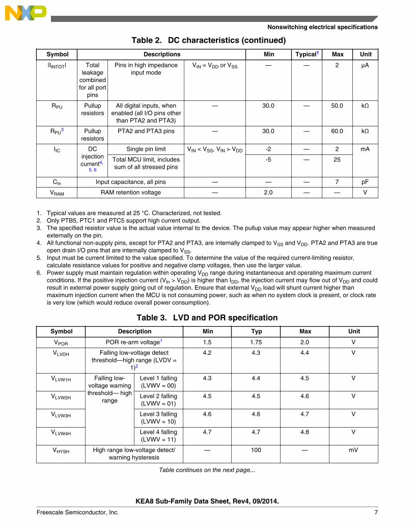
Table 2. DC characteristics (continued)
Symbol Descriptions Min Typical1 Max Unit
|IINTOT| Totalleakage
combinedfor all port
pins
Pins in high impedanceinput mode
VIN = VDD or VSS — — 2 µA
RPU Pullupresistors
All digital inputs, whenenabled (all I/O pins other
than PTA2 and PTA3)
— 30.0 — 50.0 kΩ
RPU3 Pullup
resistorsPTA2 and PTA3 pins — 30.0 — 60.0 kΩ
IIC DCinjectioncurrent4,
5, 6
Single pin limit VIN < VSS, VIN > VDD -2 — 2 mA
Total MCU limit, includessum of all stressed pins
-5 — 25
CIn Input capacitance, all pins — — — 7 pF
VRAM RAM retention voltage — 2.0 — — V
1. Typical values are measured at 25 °C. Characterized, not tested.2. Only PTB5, PTC1 and PTC5 support high current output.3. The specified resistor value is the actual value internal to the device. The pullup value may appear higher when measured
externally on the pin.4. All functional non-supply pins, except for PTA2 and PTA3, are internally clamped to VSS and VDD. PTA2 and PTA3 are true
open drain I/O pins that are internally clamped to VSS.5. Input must be current limited to the value specified. To determine the value of the required current-limiting resistor,
calculate resistance values for positive and negative clamp voltages, then use the larger value.6. Power supply must maintain regulation within operating VDD range during instantaneous and operating maximum current
conditions. If the positive injection current (VIn > VDD) is higher than IDD, the injection current may flow out of VDD and couldresult in external power supply going out of regulation. Ensure that external VDD load will shunt current higher thanmaximum injection current when the MCU is not consuming power, such as when no system clock is present, or clock rateis very low (which would reduce overall power consumption).
Table 3. LVD and POR specification
Symbol Description Min Typ Max Unit
VPOR POR re-arm voltage1 1.5 1.75 2.0 V
VLVDH Falling low-voltage detectthreshold—high range (LVDV =
1)2
4.2 4.3 4.4 V
VLVW1H Falling low-voltage warningthreshold— high
range
Level 1 falling(LVWV = 00)
4.3 4.4 4.5 V
VLVW2H Level 2 falling(LVWV = 01)
4.5 4.5 4.6 V
VLVW3H Level 3 falling(LVWV = 10)
4.6 4.6 4.7 V
VLVW4H Level 4 falling(LVWV = 11)
4.7 4.7 4.8 V
VHYSH High range low-voltage detect/warning hysteresis
— 100 — mV
Table continues on the next page...
Nonswitching electrical specifications
KEA8 Sub-Family Data Sheet, Rev4, 09/2014.
Freescale Semiconductor, Inc. 7

Table 3. LVD and POR specification (continued)
Symbol Description Min Typ Max Unit
VLVDL Falling low-voltage detectthreshold—low range (LVDV = 0)
2.56 2.61 2.66 V
VLVW1L Falling low-voltage warningthreshold—low
range
Level 1 falling(LVWV = 00)
2.62 2.7 2.78 V
VLVW2L Level 2 falling(LVWV = 01)
2.72 2.8 2.88 V
VLVW3L Level 3 falling(LVWV = 10)
2.82 2.9 2.98 V
VLVW4L Level 4 falling(LVWV = 11)
2.92 3.0 3.08 V
VHYSDL Low range low-voltage detecthysteresis
— 40 — mV
VHYSWL Low range low-voltage warninghysteresis
— 80 — mV
VBG Buffered bandgap output 3 1.14 1.16 1.18 V
1. Maximum is highest voltage that POR is guaranteed.2. Rising thresholds are falling threshold + hysteresis.3. voltage Factory trimmed at VDD = 5.0 V, Temp = 125 °C
IOH(mA)
VDD-VOH(V)
Figure 1. Typical VDD-VOH Vs. IOH (standard drive strength) (VDD = 5 V)
Nonswitching electrical specifications
KEA8 Sub-Family Data Sheet, Rev4, 09/2014.
8 Freescale Semiconductor, Inc.
IOH(mA)
VDD-VOH(V)
Figure 2. Typical VDD-VOH Vs. IOH (standard drive strength) (VDD = 3 V)
IOH(mA)
VDD-VOH(V)
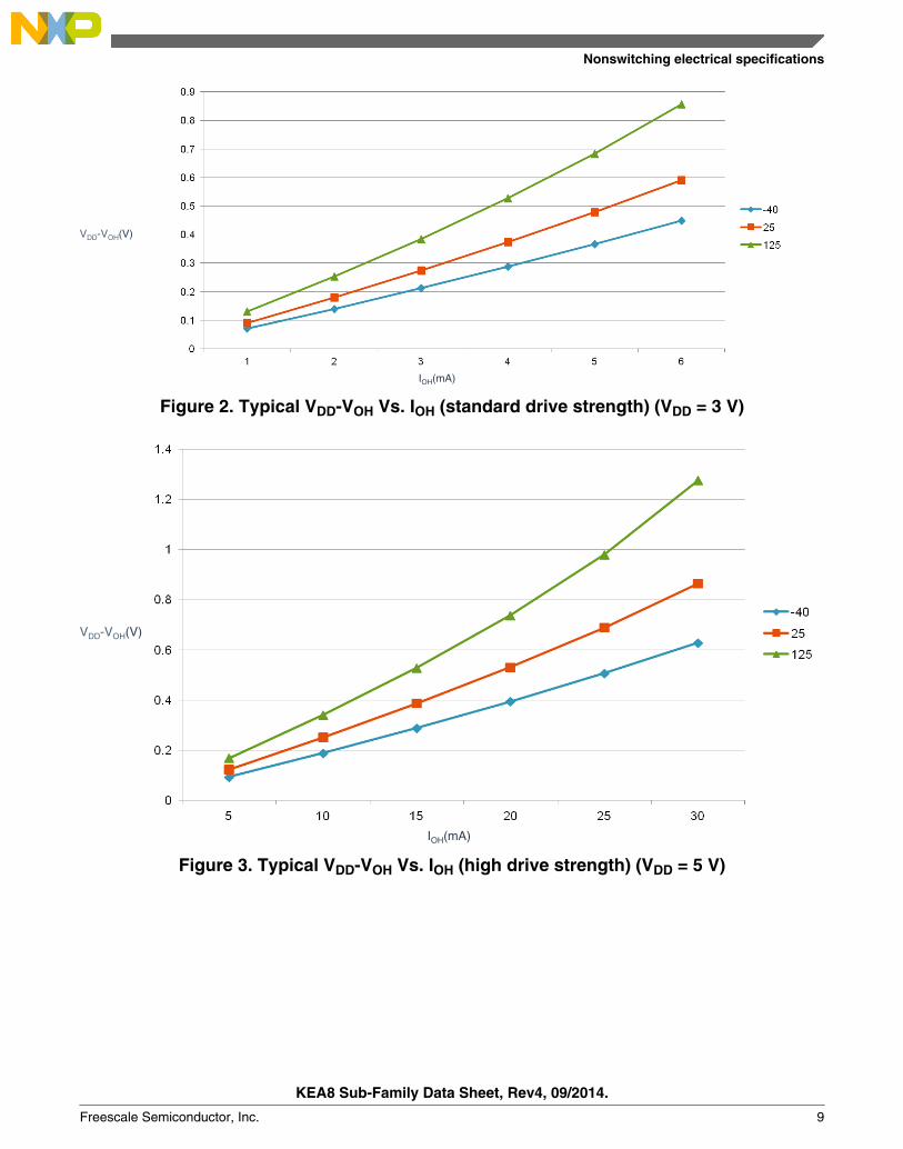
Figure 3. Typical VDD-VOH Vs. IOH (high drive strength) (VDD = 5 V)
Nonswitching electrical specifications
KEA8 Sub-Family Data Sheet, Rev4, 09/2014.
Freescale Semiconductor, Inc. 9
IOH(mA)
VDD-VOH(V)
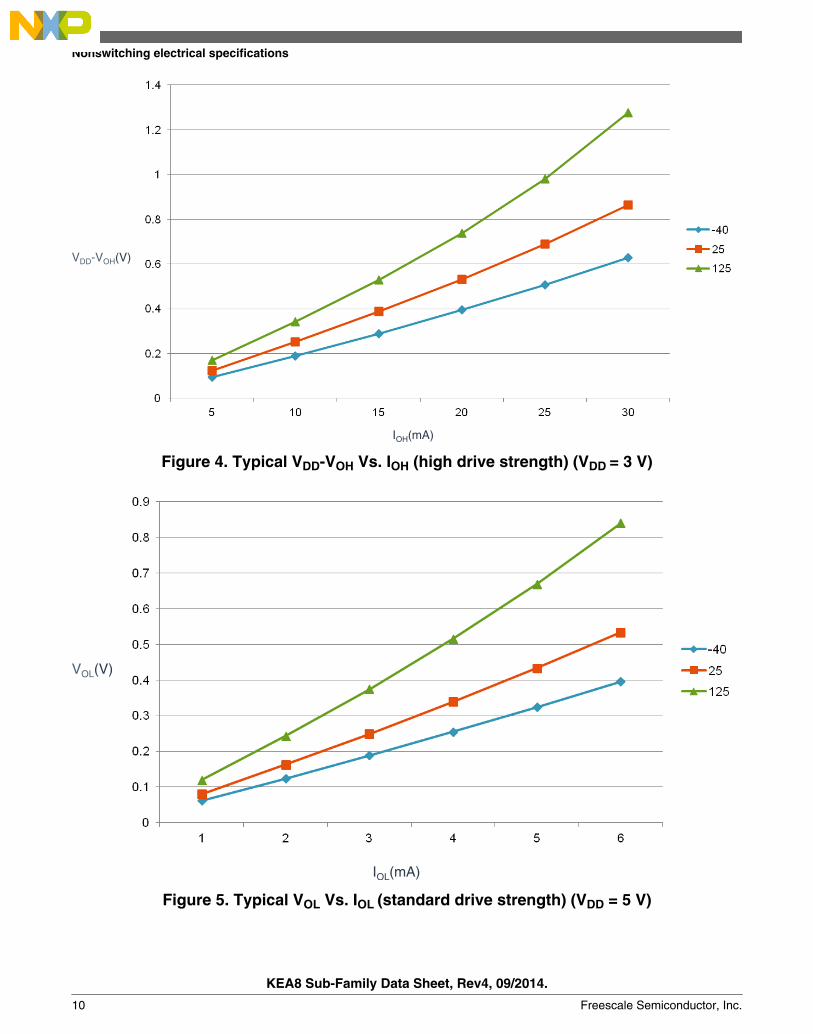
Figure 4. Typical VDD-VOH Vs. IOH (high drive strength) (VDD = 3 V)
IOL(mA)
VOL(V)
Figure 5. Typical VOL Vs. IOL (standard drive strength) (VDD = 5 V)
Nonswitching electrical specifications
KEA8 Sub-Family Data Sheet, Rev4, 09/2014.
10 Freescale Semiconductor, Inc.
IOL(mA)
VOL(V)
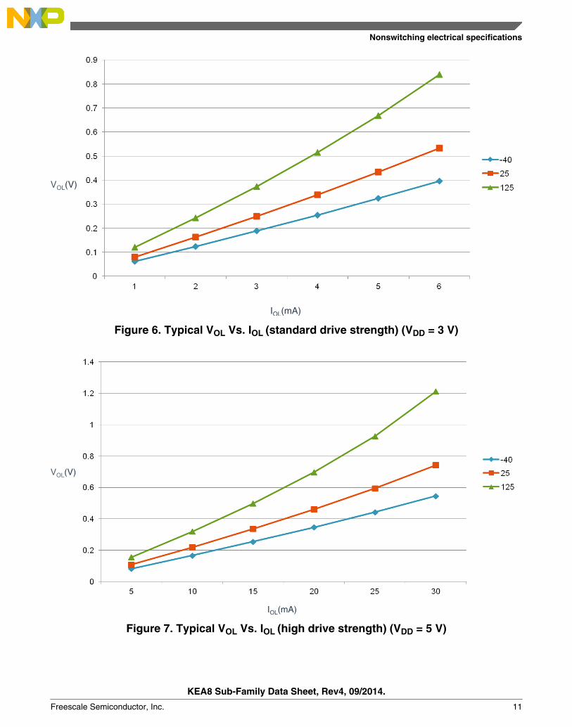
Figure 6. Typical VOL Vs. IOL (standard drive strength) (VDD = 3 V)
IOL(mA)
VOL(V)
Figure 7. Typical VOL Vs. IOL (high drive strength) (VDD = 5 V)
Nonswitching electrical specifications
KEA8 Sub-Family Data Sheet, Rev4, 09/2014.
Freescale Semiconductor, Inc. 11
IOL(mA)
VOL(V)
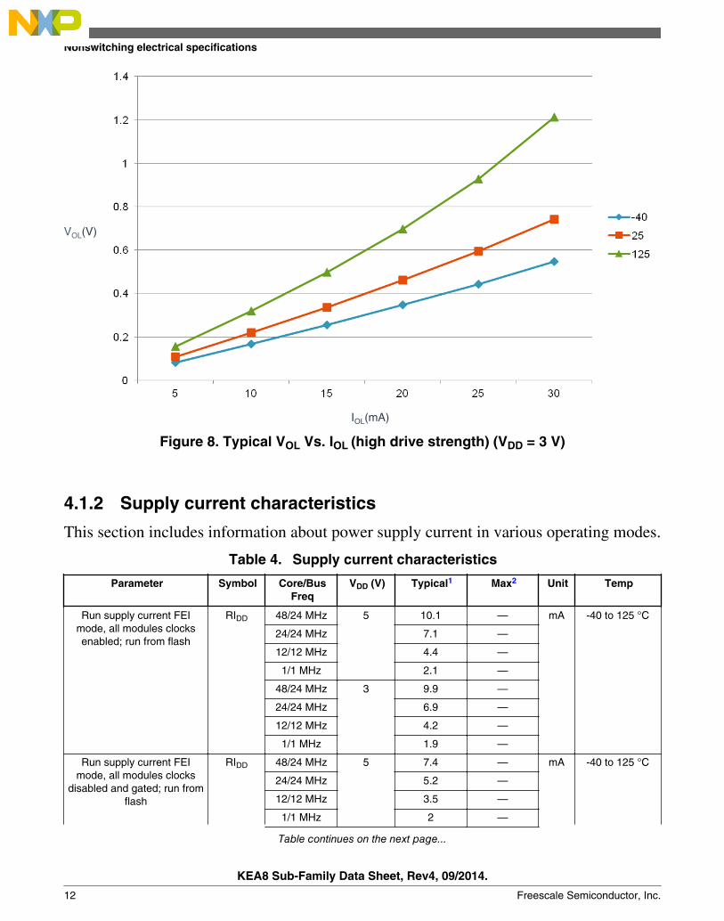
Figure 8. Typical VOL Vs. IOL (high drive strength) (VDD = 3 V)
4.1.2 Supply current characteristics
This section includes information about power supply current in various operating modes.
Table 4. Supply current characteristics
Parameter Symbol Core/BusFreq
VDD (V) Typical1 Max2 Unit Temp
Run supply current FEImode, all modules clocksenabled; run from flash
RIDD 48/24 MHz 5 10.1 — mA -40 to 125 °C
24/24 MHz 7.1 —
12/12 MHz 4.4 —
1/1 MHz 2.1 —
48/24 MHz 3 9.9 —
24/24 MHz 6.9 —
12/12 MHz 4.2 —
1/1 MHz 1.9 —
Run supply current FEImode, all modules clocks
disabled and gated; run fromflash
RIDD 48/24 MHz 5 7.4 — mA -40 to 125 °C
24/24 MHz 5.2 —
12/12 MHz 3.5 —
1/1 MHz 2 —
Table continues on the next page...
Nonswitching electrical specifications
KEA8 Sub-Family Data Sheet, Rev4, 09/2014.
12 Freescale Semiconductor, Inc.

Table 4. Supply current characteristics (continued)
Parameter Symbol Core/BusFreq
VDD (V) Typical1 Max2 Unit Temp
48/24 MHz 3 7.2 —
24/24 MHz 5 —
12/12 MHz 3.3 —
1/1 MHz 1.8 —
Run supply current FBEmode, all modules clocksenabled; run from RAM
RIDD 48/24 MHz 5 13.2 — mA -40 to 125 °C
24/24 MHz 9.1 10.8
12/12 MHz 5.1 —
1/1 MHz 1.8 —
48/24 MHz 3 13 —
24/24 MHz 9 10.7
12/12 MHz 5 —
1/1 MHz 1.7 —
Run supply current FBEmode, all modules clocks
disabled and gated; run fromRAM
RIDD 48/24 MHz 5 10.6 — mA -40 to 125 °C
24/24 MHz 7.6 9.2
12/12 MHz 4.3 —
1/1 MHz 1.7 —
48/24 MHz 3 10.5 —
24/24 MHz 7.5 9.1
12/12 MHz 4.2 —
1/1 MHz 1.6 —
Wait mode current FEImode, all modules clocks
enabled
WIDD 48/24 MHz 5 7.2 — mA -40 to 125 °C
24/24 MHz 6.3 7.4
12/12 MHz 3.6 —
1/1 MHz 1.9 —
48/24 MHz 3 7.1 —
24/24 MHz 6.2 7.3
12/12 MHz 3.5 —
1/1 MHz 1.8 —
Stop mode supply current noclocks active (except 1 kHz
LPO clock)3, 4
SIDD — 5 2 110 µA -40 to 125 °C
— 3 1.9 105 -40 to 125 °C
ADC adder to Stop
ADLPC = 1
ADLSMP = 1
ADCO = 1
MODE = 10B
ADICLK = 11B
— — 5 86 — µA -40 to 125 °C
3 82 —
LVD adder to Stop5 — — 5 130 — µA -40 to 125 °C
3 125 —
Nonswitching electrical specifications
KEA8 Sub-Family Data Sheet, Rev4, 09/2014.
Freescale Semiconductor, Inc. 13
1. Data in Typical column was characterized at 5.0 V, 25 °C or is typical recommended value.2. The Max current is observed at high temperature of 125 °C.3. RTC adder cause <1 µA IDD increase typically, RTC clock source is 1 kHz LPO clock.4. ACMP adder cause <1 µA IDD increase typically.5. LVD is periodically woken up from Stop by 5% duty cycle. The period is equal to or less than 2 ms.
4.1.3 EMC performanceElectromagnetic compatibility (EMC) performance is highly dependent on theenvironment in which the MCU resides. Board design and layout, circuit topologychoices, location and characteristics of external components as well as MCU softwareoperation play a significant role in EMC performance. The system designer must consultthe following Freescale applications notes, available on freescale.com for advice andguidance specifically targeted at optimizing EMC performance.
• AN2321: Designing for Board Level Electromagnetic Compatibility• AN1050: Designing for Electromagnetic Compatibility (EMC) with HCMOS
Microcontrollers• AN1263: Designing for Electromagnetic Compatibility with Single-Chip
Microcontrollers• AN2764: Improving the Transient Immunity Performance of Microcontroller-Based
Applications• AN1259: System Design and Layout Techniques for Noise Reduction in MCU-
Based Systems
Switching specifications
4.2.1 Control timingTable 5. Control timing
Num Rating Symbol Min Typical1 Max Unit
1 System and core clock fSys DC — 48 MHz
2 Bus frequency (tcyc = 1/fBus) fBus DC — 24 MHz
3 Internal low power oscillator frequency fLPO 0.67 1.0 1.25 KHz
4 External reset pulse width2 textrst 1.5 ×
tcyc
— — ns
5 Reset low drive trstdrv 34 × tcyc — — ns
6 IRQ pulse width Asynchronous path2 tILIH 100 — — ns
Synchronous path3 tIHIL 1.5 × tcyc — — ns
7 Keyboard interrupt pulsewidth
Asynchronous path2 tILIH 100 — — ns
Synchronous path tIHIL 1.5 × tcyc — — ns
Table continues on the next page...
4.2
Switching specifications
KEA8 Sub-Family Data Sheet, Rev4, 09/2014.
14 Freescale Semiconductor, Inc.
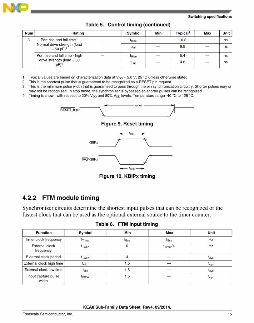
Table 5. Control timing (continued)
Num Rating Symbol Min Typical1 Max Unit
8 Port rise and fall time -Normal drive strength (load
= 50 pF)4
— tRise — 10.2 — ns
tFall — 9.5 — ns
Port rise and fall time - highdrive strength (load = 50
pF)4
— tRise — 5.4 — ns
tFall — 4.6 — ns
1. Typical values are based on characterization data at VDD = 5.0 V, 25 °C unless otherwise stated.2. This is the shortest pulse that is guaranteed to be recognized as a RESET pin request.3. This is the minimum pulse width that is guaranteed to pass through the pin synchronization circuitry. Shorter pulses may or
may not be recognized. In stop mode, the synchronizer is bypassed so shorter pulses can be recognized.4. Timing is shown with respect to 20% VDD and 80% VDD levels. Temperature range -40 °C to 125 °C.
textrst
RESET_b pin
Figure 9. Reset timing
tIHIL
KBIPx
tILIH
IRQ/KBIPx
Figure 10. KBIPx timing
4.2.2 FTM module timing
Synchronizer circuits determine the shortest input pulses that can be recognized or thefastest clock that can be used as the optional external source to the timer counter.
Table 6. FTM input timing
Function Symbol Min Max Unit
Timer clock frequency fTimer fBus fSys Hz
External clockfrequency
fTCLK 0 fTimer/4 Hz
External clock period tTCLK 4 — tcyc
External clock high time tclkh 1.5 — tcyc
External clock low time tclkl 1.5 — tcyc
Input capture pulsewidth
tICPW 1.5 — tcyc
Switching specifications
KEA8 Sub-Family Data Sheet, Rev4, 09/2014.
Freescale Semiconductor, Inc. 15
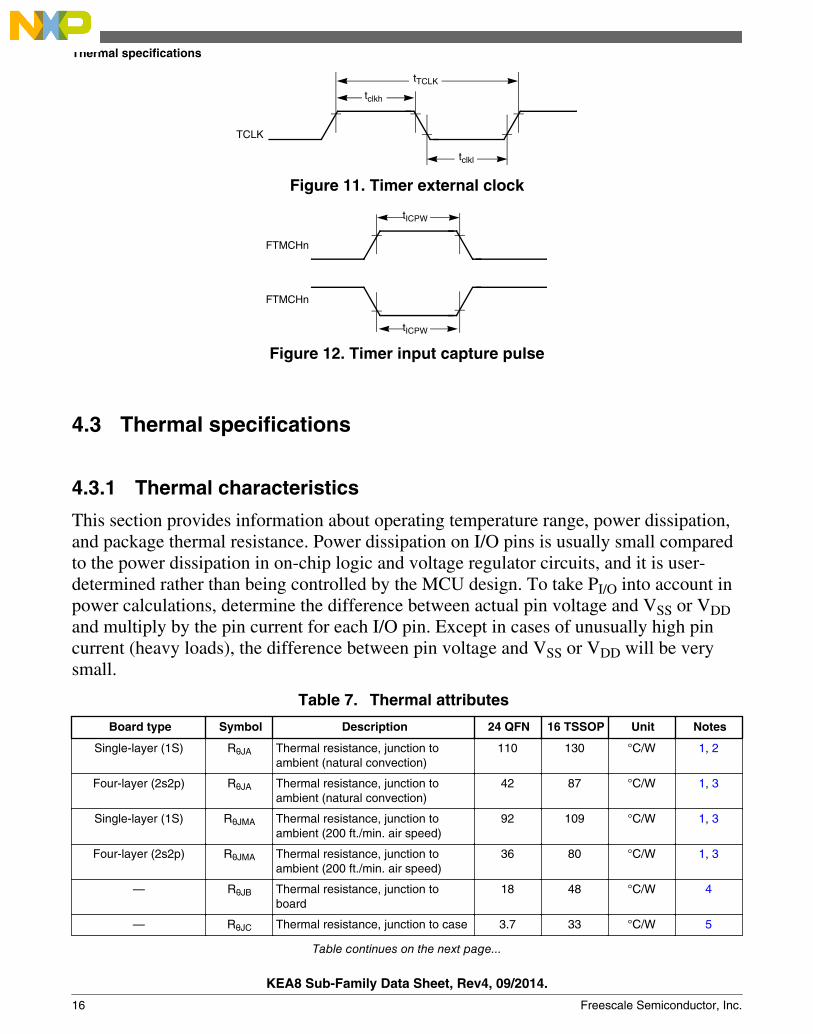
tTCLK
tclkh
tclkl
TCLK
Figure 11. Timer external clock
tICPW
FTMCHn
tICPW
FTMCHn
Figure 12. Timer input capture pulse
Thermal specifications
4.3.1 Thermal characteristics
This section provides information about operating temperature range, power dissipation,and package thermal resistance. Power dissipation on I/O pins is usually small comparedto the power dissipation in on-chip logic and voltage regulator circuits, and it is user-determined rather than being controlled by the MCU design. To take PI/O into account inpower calculations, determine the difference between actual pin voltage and VSS or VDDand multiply by the pin current for each I/O pin. Except in cases of unusually high pincurrent (heavy loads), the difference between pin voltage and VSS or VDD will be verysmall.
Table 7. Thermal attributes
Board type Symbol Description 24 QFN 16 TSSOP Unit Notes
Single-layer (1S) RθJA Thermal resistance, junction toambient (natural convection)
110 130 °C/W 1, 2
Four-layer (2s2p) RθJA Thermal resistance, junction toambient (natural convection)
42 87 °C/W 1, 3
Single-layer (1S) RθJMA Thermal resistance, junction toambient (200 ft./min. air speed)
92 109 °C/W 1, 3
Four-layer (2s2p) RθJMA Thermal resistance, junction toambient (200 ft./min. air speed)
36 80 °C/W 1, 3
— RθJB Thermal resistance, junction toboard
18 48 °C/W 4
— RθJC Thermal resistance, junction to case 3.7 33 °C/W 5
Table continues on the next page...
4.3
Thermal specifications
KEA8 Sub-Family Data Sheet, Rev4, 09/2014.
16 Freescale Semiconductor, Inc.
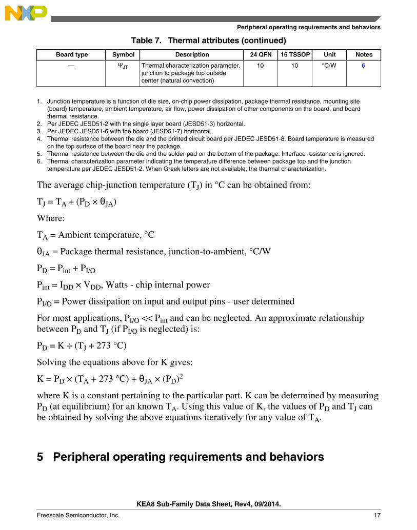
Table 7. Thermal attributes (continued)
Board type Symbol Description 24 QFN 16 TSSOP Unit Notes
— ΨJT Thermal characterization parameter,junction to package top outsidecenter (natural convection)
10 10 °C/W 6
1. Junction temperature is a function of die size, on-chip power dissipation, package thermal resistance, mounting site(board) temperature, ambient temperature, air flow, power dissipation of other components on the board, and boardthermal resistance.
2. Per JEDEC JESD51-2 with the single layer board (JESD51-3) horizontal.3. Per JEDEC JESD51-6 with the board (JESD51-7) horizontal.4. Thermal resistance between the die and the printed circuit board per JEDEC JESD51-8. Board temperature is measured
on the top surface of the board near the package.5. Thermal resistance between the die and the solder pad on the bottom of the package. Interface resistance is ignored.6. Thermal characterization parameter indicating the temperature difference between package top and the junction
temperature per JEDEC JESD51-2. When Greek letters are not available, the thermal characterization.
The average chip-junction temperature (TJ) in °C can be obtained from:
TJ = TA + (PD × θJA)
Where:
TA = Ambient temperature, °C
θJA = Package thermal resistance, junction-to-ambient, °C/W
PD = Pint + PI/O
Pint = IDD × VDD, Watts - chip internal power
PI/O = Power dissipation on input and output pins - user determined
For most applications, PI/O << Pint and can be neglected. An approximate relationshipbetween PD and TJ (if PI/O is neglected) is:
PD = K ÷ (TJ + 273 °C)
Solving the equations above for K gives:
K = PD × (TA + 273 °C) + θJA × (PD)2
where K is a constant pertaining to the particular part. K can be determined by measuringPD (at equilibrium) for an known TA. Using this value of K, the values of PD and TJ canbe obtained by solving the above equations iteratively for any value of TA.
5 Peripheral operating requirements and behaviors
Peripheral operating requirements and behaviors
KEA8 Sub-Family Data Sheet, Rev4, 09/2014.
Freescale Semiconductor, Inc. 17
5.1 Core modules
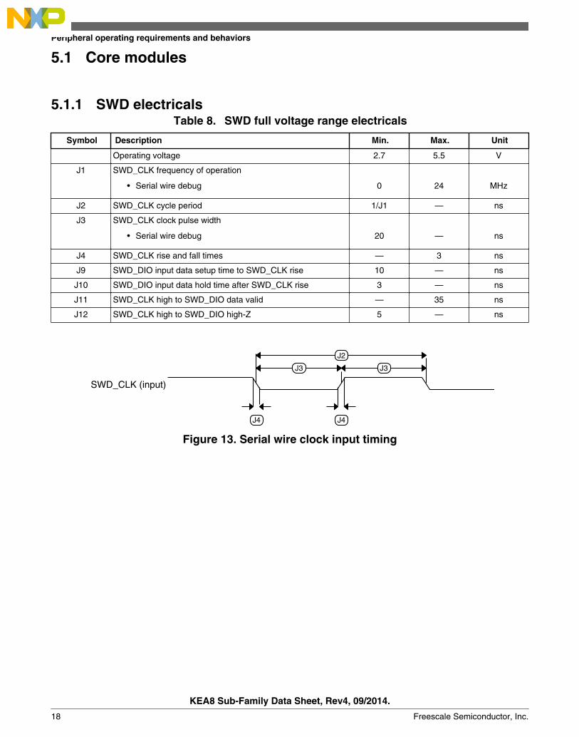
5.1.1 SWD electricalsTable 8. SWD full voltage range electricals
Symbol Description Min. Max. Unit
Operating voltage 2.7 5.5 V
J1 SWD_CLK frequency of operation
• Serial wire debug
0
24
MHz
J2 SWD_CLK cycle period 1/J1 — ns
J3 SWD_CLK clock pulse width
• Serial wire debug
20
—
ns
J4 SWD_CLK rise and fall times — 3 ns
J9 SWD_DIO input data setup time to SWD_CLK rise 10 — ns
J10 SWD_DIO input data hold time after SWD_CLK rise 3 — ns
J11 SWD_CLK high to SWD_DIO data valid — 35 ns
J12 SWD_CLK high to SWD_DIO high-Z 5 — ns
J2
J3 J3
J4 J4
SWD_CLK (input)
Figure 13. Serial wire clock input timing
Peripheral operating requirements and behaviors
KEA8 Sub-Family Data Sheet, Rev4, 09/2014.
18 Freescale Semiconductor, Inc.

J11
J12
J11
J9 J10
Input data valid
Output data valid
Output data valid
SWD_CLK
SWD_DIO
SWD_DIO
SWD_DIO
SWD_DIO
Figure 14. Serial wire data timing
5.2 External oscillator (OSC) and ICS characteristicsTable 9. OSC and ICS specifications (temperature range = -40 to 125 °C ambient)
Num Characteristic Symbol Min Typical1 Max Unit
1 Crystal orresonatorfrequency
Low range (RANGE = 0) flo 31.25 32.768 39.0625 kHz
High range (RANGE = 1) fhi 4 — 24 MHz
2 Load capacitors C1, C2 See Note2
3 Feedbackresistor
Low Frequency, Low-PowerMode3
RF — — — MΩ
Low Frequency, High-GainMode
— 10 — MΩ
High Frequency, Low-PowerMode
— 1 — MΩ
High Frequency, High-GainMode
— 1 — MΩ
4 Series resistor -Low Frequency
Low-Power Mode 3 RS — 0 — kΩ
High-Gain Mode — 200 — kΩ
5 Series resistor -High Frequency
Low-Power Mode3 RS — 0 — kΩ
Series resistor -High Frequency,High-Gain Mode
4 MHz — 0 — kΩ
8 MHz — 0 — kΩ
Table continues on the next page...
Peripheral operating requirements and behaviors
KEA8 Sub-Family Data Sheet, Rev4, 09/2014.
Freescale Semiconductor, Inc. 19
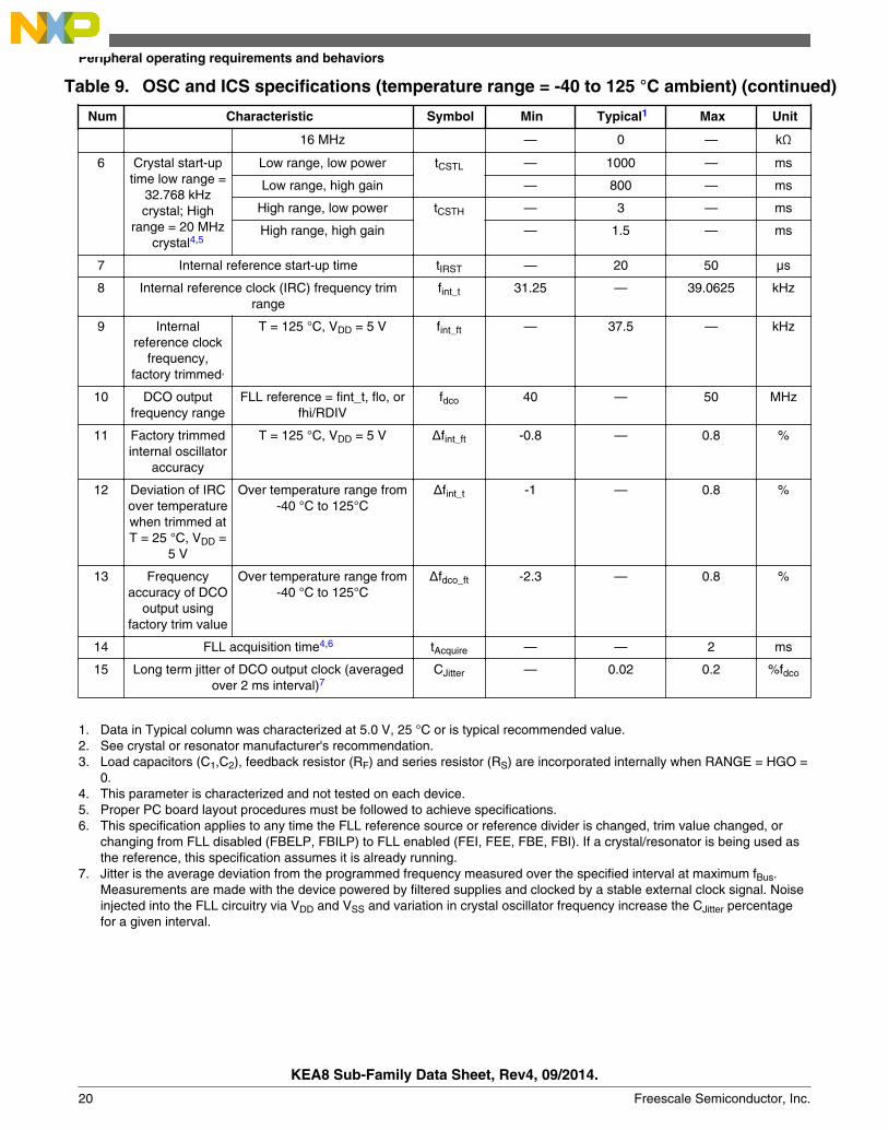
Table 9. OSC and ICS specifications (temperature range = -40 to 125 °C ambient) (continued)
Num Characteristic Symbol Min Typical1 Max Unit
16 MHz — 0 — kΩ
6 Crystal start-uptime low range =
32.768 kHzcrystal; High
range = 20 MHzcrystal4,5
Low range, low power tCSTL — 1000 — ms
Low range, high gain — 800 — ms
High range, low power tCSTH — 3 — ms
High range, high gain — 1.5 — ms
7 Internal reference start-up time tIRST — 20 50 µs
8 Internal reference clock (IRC) frequency trimrange
fint_t 31.25 — 39.0625 kHz
9 Internalreference clock
frequency,factory trimmed,
T = 125 °C, VDD = 5 V fint_ft — 37.5 — kHz
10 DCO outputfrequency range
FLL reference = fint_t, flo, orfhi/RDIV
fdco 40 — 50 MHz
11 Factory trimmedinternal oscillator
accuracy
T = 125 °C, VDD = 5 V Δfint_ft -0.8 — 0.8 %
12 Deviation of IRCover temperaturewhen trimmed atT = 25 °C, VDD =
5 V
Over temperature range from-40 °C to 125°C
Δfint_t -1 — 0.8 %
13 Frequencyaccuracy of DCO
output usingfactory trim value
Over temperature range from-40 °C to 125°C
Δfdco_ft -2.3 — 0.8 %
14 FLL acquisition time4,6 tAcquire — — 2 ms
15 Long term jitter of DCO output clock (averagedover 2 ms interval)7
CJitter — 0.02 0.2 %fdco
1. Data in Typical column was characterized at 5.0 V, 25 °C or is typical recommended value.2. See crystal or resonator manufacturer's recommendation.3. Load capacitors (C1,C2), feedback resistor (RF) and series resistor (RS) are incorporated internally when RANGE = HGO =
0.4. This parameter is characterized and not tested on each device.5. Proper PC board layout procedures must be followed to achieve specifications.6. This specification applies to any time the FLL reference source or reference divider is changed, trim value changed, or
changing from FLL disabled (FBELP, FBILP) to FLL enabled (FEI, FEE, FBE, FBI). If a crystal/resonator is being used asthe reference, this specification assumes it is already running.
7. Jitter is the average deviation from the programmed frequency measured over the specified interval at maximum fBus.Measurements are made with the device powered by filtered supplies and clocked by a stable external clock signal. Noiseinjected into the FLL circuitry via VDD and VSS and variation in crystal oscillator frequency increase the CJitter percentagefor a given interval.
Peripheral operating requirements and behaviors
KEA8 Sub-Family Data Sheet, Rev4, 09/2014.
20 Freescale Semiconductor, Inc.
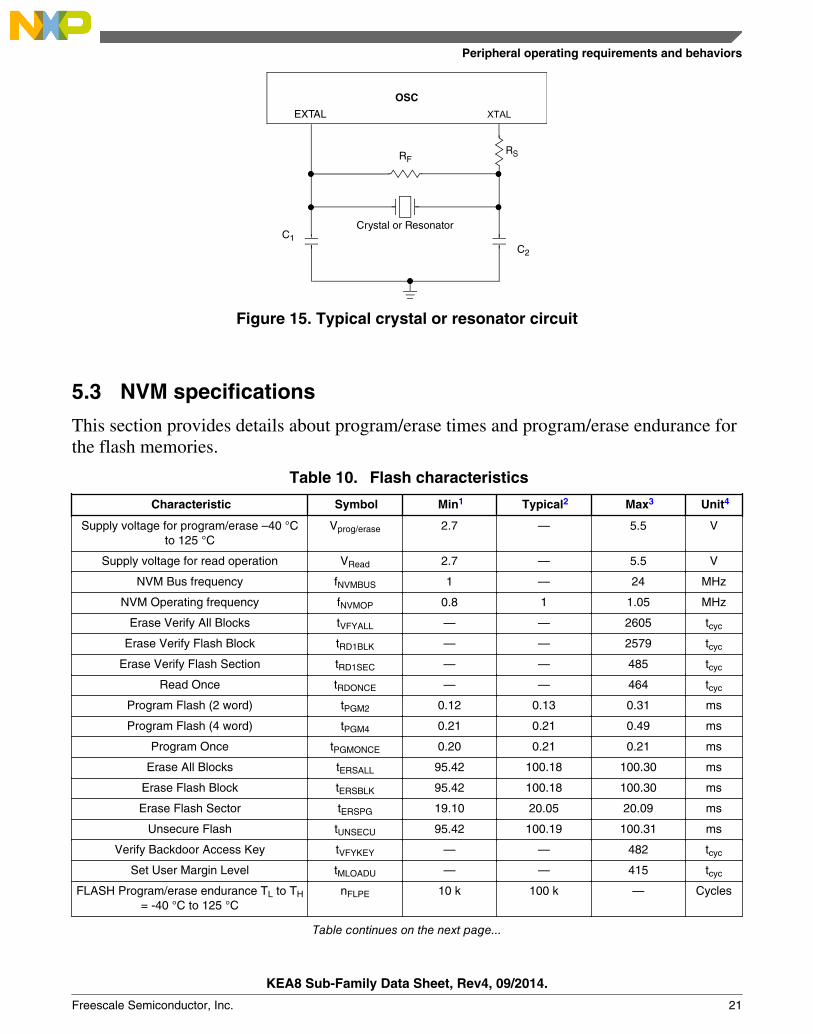
OSC
EXTAL
Crystal or Resonator
RS
C2
RF
C1
XTAL
Figure 15. Typical crystal or resonator circuit
5.3 NVM specifications
This section provides details about program/erase times and program/erase endurance forthe flash memories.
Table 10. Flash characteristics
Characteristic Symbol Min1 Typical2 Max3 Unit4
Supply voltage for program/erase –40 °Cto 125 °C
Vprog/erase 2.7 — 5.5 V
Supply voltage for read operation VRead 2.7 — 5.5 V
NVM Bus frequency fNVMBUS 1 — 24 MHz
NVM Operating frequency fNVMOP 0.8 1 1.05 MHz
Erase Verify All Blocks tVFYALL — — 2605 tcyc
Erase Verify Flash Block tRD1BLK — — 2579 tcyc
Erase Verify Flash Section tRD1SEC — — 485 tcyc
Read Once tRDONCE — — 464 tcyc
Program Flash (2 word) tPGM2 0.12 0.13 0.31 ms
Program Flash (4 word) tPGM4 0.21 0.21 0.49 ms
Program Once tPGMONCE 0.20 0.21 0.21 ms
Erase All Blocks tERSALL 95.42 100.18 100.30 ms
Erase Flash Block tERSBLK 95.42 100.18 100.30 ms
Erase Flash Sector tERSPG 19.10 20.05 20.09 ms
Unsecure Flash tUNSECU 95.42 100.19 100.31 ms
Verify Backdoor Access Key tVFYKEY — — 482 tcyc
Set User Margin Level tMLOADU — — 415 tcyc
FLASH Program/erase endurance TL to TH= -40 °C to 125 °C
nFLPE 10 k 100 k — Cycles
Table continues on the next page...
Peripheral operating requirements and behaviors
KEA8 Sub-Family Data Sheet, Rev4, 09/2014.
Freescale Semiconductor, Inc. 21
Table 10. Flash characteristics (continued)
Characteristic Symbol Min1 Typical2 Max3 Unit4
Data retention at an average junctiontemperature of TJavg = 85°C after up to
10,000 program/erase cycles
tD_ret 15 100 — years
1. Minimum times are based on maximum fNVMOP and maximum fNVMBUS2. Typical times are based on typical fNVMOP and maximum fNVMBUS3. Maximum times are based on typical fNVMOP and typical fNVMBUS plus aging4. tcyc = 1 / fNVMBUS
Program and erase operations do not require any special power sources other than thenormal VDD supply. For more detailed information about program/erase operations, seethe Flash Memory Module section in the reference manual.
5.4 Analog
5.4.1 ADC characteristicsTable 11. 5 V 12-bit ADC operating conditions
Characteristic
Conditions Symbol Min Typ1 Max Unit Comment
Supplyvoltage
Absolute VDDA 2.7 — 5.5 V —
Delta to VDD (VDD-VDDA) ΔVDDA -100 0 +100 mV —
Inputvoltage
VADIN VREFL — VREFH V —
Inputcapacitance
CADIN — 4.5 5.5 pF —
Inputresistance
RADIN — 3 5 kΩ —
Analogsource
resistance
12-bit mode• fADCK > 4 MHz• fADCK < 4 MHz
RAS —
—
—
—
2
5
kΩ External toMCU
10-bit mode• fADCK > 4 MHz• fADCK < 4 MHz
—
—
—
—
5
10
8-bit mode
(all valid fADCK)
— — 10
ADCconversion
clockfrequency
High speed (ADLPC=0) fADCK 0.4 — 8.0 MHz —
Low power (ADLPC=1) 0.4 — 4.0
1. Typical values assume VDDA = 5.0 V, Temp = 25°C, fADCK=1.0 MHz unless otherwise stated. Typical values are forreference only and are not tested in production.
Peripheral operating requirements and behaviors
KEA8 Sub-Family Data Sheet, Rev4, 09/2014.
22 Freescale Semiconductor, Inc.
ADC SAR ENGINE
SIMPLIFIED CHANNEL SELECT
CIRCUIT
SIMPLIFIED INPUT PIN EQUIVALENT
CIRCUITPad leakage due to input protection
ZAS
R AS
C AS
v ADIN
v AS
z ADIN
R ADIN
R ADIN
R ADIN
R ADIN
INPUT PIN
INPUT PIN
INPUT PIN C ADIN
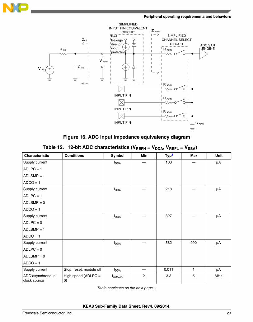
Figure 16. ADC input impedance equivalency diagram
Table 12. 12-bit ADC characteristics (VREFH = VDDA, VREFL = VSSA)
Characteristic Conditions Symbol Min Typ1 Max Unit
Supply current
ADLPC = 1
ADLSMP = 1
ADCO = 1
IDDA — 133 — µA
Supply current
ADLPC = 1
ADLSMP = 0
ADCO = 1
IDDA — 218 — µA
Supply current
ADLPC = 0
ADLSMP = 1
ADCO = 1
IDDA — 327 — µA
Supply current
ADLPC = 0
ADLSMP = 0
ADCO = 1
IDDA — 582 990 µA
Supply current Stop, reset, module off IDDA — 0.011 1 µA
ADC asynchronousclock source
High speed (ADLPC =0)
fADACK 2 3.3 5 MHz
Table continues on the next page...
Peripheral operating requirements and behaviors
KEA8 Sub-Family Data Sheet, Rev4, 09/2014.
Freescale Semiconductor, Inc. 23
Table 12. 12-bit ADC characteristics (VREFH = VDDA, VREFL = VSSA) (continued)
Characteristic Conditions Symbol Min Typ1 Max Unit
Low power (ADLPC =1)
1.25 2 3.3
Conversion time(including sample time)
Short sample(ADLSMP = 0)
tADC — 20 — ADCK cycles
Long sample(ADLSMP = 1)
— 40 —
Sample time Short sample(ADLSMP = 0)
tADS — 3.5 — ADCK cycles
Long sample(ADLSMP = 1)
— 23.5 —
Total unadjusted Error2 12-bit mode ETUE — ±3.0 — LSB3
10-bit mode — ±1.0 ±6.0
8-bit mode — ±0.8 —
Differential Non-Liniarity
12-bit mode DNL — ±1.2 — LSB3
10-bit mode4 — ±0.3 ±4.0
8-bit mode4 — ±0.15 —
Integral Non-Linearity 12-bit mode INL — ±1.2 — LSB3
10-bit mode — ±0.3 ±5.0
8-bit mode — ±0.15 —
Zero-scale error5 12-bit mode EZS — ±1.2 — LSB3
10-bit mode — ±0.15 ±6.0
8-bit mode — ±0.3 —
Full-scale error6 12-bit mode EFS — ±1.8 — LSB3
10-bit mode — ±0.7 ±1.0
8-bit mode — ±0.5 —
Quantization error ≤12 bit modes EQ — — ±0.5 LSB3
Input leakage error7 all modes EIL IIn x RAS mV
Temp sensor slope -40 °C–25 °C m — 3.266 — mV/°C
25 °C–125 °C — 3.638 —
Temp sensor voltage 25 °C VTEMP25 — 1.396 — V
1. Typical values assume VDDA = 5.0 V, Temp = 25 °C, fADCK=2.5 MHz under FBE mode and alternate clock source(ALTCLK) is selected as ADC clock.
2. Includes quantization3. 1 LSB = (VREFH - VREFL)/2N
4. Monotonicity and no-missing-codes guaranteed in 10-bit and 8-bit modes5. VADIN = VSSA6. VADIN = VDDA7. IIn = leakage current (refer to DC characteristics)
Peripheral operating requirements and behaviors
KEA8 Sub-Family Data Sheet, Rev4, 09/2014.
24 Freescale Semiconductor, Inc.
5.4.2 Analog comparator (ACMP) electricalsTable 13. Comparator electrical specifications
Characteristic Symbol Min Typical Max Unit
Supply voltage VDDA 2.7 — 5.5 V
Supply current (Operation mode) IDDA — 10 20 µA
Analog input voltage VAIN VSS - 0.3 — VDDA V
Analog input offset voltage VAIO — — 40 mV
Analog comparator hysteresis(HYST=0)
VH — 15 20 mV
Analog comparator hysteresis(HYST=1)
VH — 20 30 mV
Supply current (Off mode) IDDAOFF — 60 — nA
Propagation Delay tD — 0.4 1 µs
5.5 Communication interfaces
5.5.1 SPI switching specifications
The serial peripheral interface (SPI) provides a synchronous serial bus with master andslave operations. Many of the transfer attributes are programmable. The following tablesprovide timing characteristics for classic SPI timing modes. See the SPI chapter of thechip's reference manual for information about the modified transfer formats used forcommunicating with slower peripheral devices. All timing is shown with respect to 20%VDD and 80% VDD, unless noted, and 25 pF load on all SPI pins. All timing assumes slewrate control is disabled and high-drive strength is enabled for SPI output pins.
Table 14. SPI master mode timing
Num.
Symbol Description Min. Max. Unit Comment
1 fop Frequency of operation fBus/2048 fBus/2 Hz fBus is the busclock
2 tSPSCK SPSCK period 2 x tBus 2048 x tBus ns tBus = 1/fBus
3 tLead Enable lead time 1/2 — tSPSCK —
4 tLag Enable lag time 1/2 — tSPSCK —
5 tWSPSCK Clock (SPSCK) high or low time tBus – 30 1024 x tBus ns —
6 tSU Data setup time (inputs) 8 — ns —
7 tHI Data hold time (inputs) 8 — ns —
8 tv Data valid (after SPSCK edge) — 25 ns —
9 tHO Data hold time (outputs) 20 — ns —
Table continues on the next page...
Peripheral operating requirements and behaviors
KEA8 Sub-Family Data Sheet, Rev4, 09/2014.
Freescale Semiconductor, Inc. 25
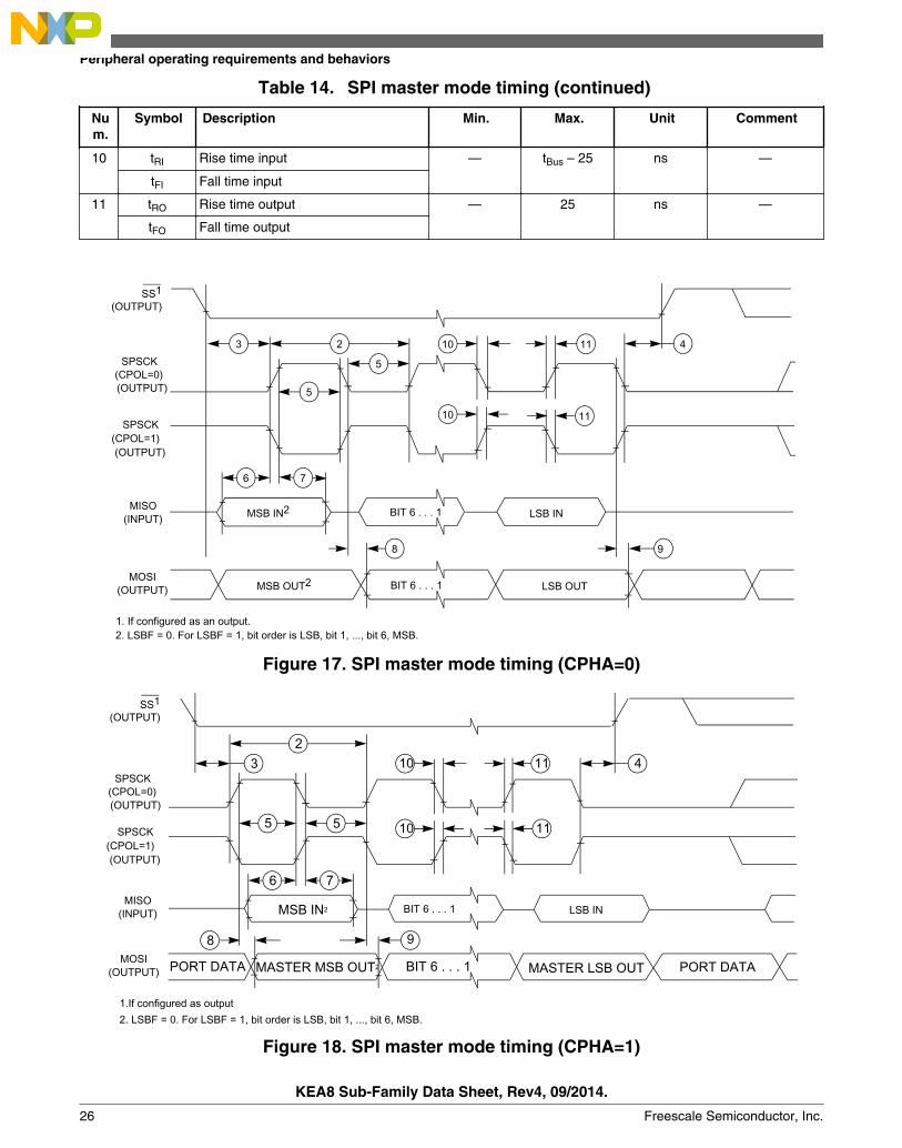
Table 14. SPI master mode timing (continued)
Num.
Symbol Description Min. Max. Unit Comment
10 tRI Rise time input — tBus – 25 ns —
tFI Fall time input
11 tRO Rise time output — 25 ns —
tFO Fall time output
(OUTPUT)
2
8
6 7
MSB IN2 LSB IN
MSB OUT2 LSB OUT
9
5
5
3
(CPOL=0)
411
1110
10SPSCK
SPSCK(CPOL=1)
2. LSBF = 0. For LSBF = 1, bit order is LSB, bit 1, ..., bit 6, MSB.1. If configured as an output.
SS1
(OUTPUT)
(OUTPUT)
MOSI(OUTPUT)
MISO(INPUT) BIT 6 . . . 1
BIT 6 . . . 1
Figure 17. SPI master mode timing (CPHA=0)
<<CLASSIFICATION>> <<NDA MESSAGE>>
38
2
6 7
MSB IN2
BIT 6 . . . 1 MASTER MSB OUT2 MASTER LSB OUT
55
8
10 11
PORT DATA PORT DATA
3 10 11 4
1.If configured as output 2. LSBF = 0. For LSBF = 1, bit order is LSB, bit 1, ..., bit 6, MSB.
9
(OUTPUT)
(CPOL=0)SPSCK
SPSCK(CPOL=1)
SS1
(OUTPUT)
(OUTPUT)
MOSI(OUTPUT)
MISO(INPUT) LSB INBIT 6 . . . 1
Figure 18. SPI master mode timing (CPHA=1)
Peripheral operating requirements and behaviors
KEA8 Sub-Family Data Sheet, Rev4, 09/2014.
26 Freescale Semiconductor, Inc.
Table 15. SPI slave mode timing
Num.
Symbol Description Min. Max. Unit Comment
1 fop Frequency of operation 0 fBus/4 Hz fBus is the bus clock asdefined in Control timing.
2 tSPSCK SPSCK period 4 x tBus — ns tBus = 1/fBus
3 tLead Enable lead time 1 — tBus —
4 tLag Enable lag time 1 — tBus —
5 tWSPSCK Clock (SPSCK) high or low time tBus - 30 — ns —
6 tSU Data setup time (inputs) 15 — ns —
7 tHI Data hold time (inputs) 25 — ns —
8 ta Slave access time — tBus ns Time to data active fromhigh-impedance state
9 tdis Slave MISO disable time — tBus ns Hold time to high-impedance state
10 tv Data valid (after SPSCK edge) — 25 ns —
11 tHO Data hold time (outputs) 0 — ns —
12 tRI Rise time input — tBus - 25 ns —
tFI Fall time input
13 tRO Rise time output — 25 ns —
tFO Fall time output
2
10
6 7
MSB IN
BIT 6 . . . 1 SLAVE MSB SLAVE LSB OUT
11
553
8
4
13
NOTE: Not defined
12
12
11
SEE NOTE
13
9
see note
(INPUT)
(CPOL=0)SPSCK
SPSCK(CPOL=1)
SS
(INPUT)
(INPUT)
MOSI(INPUT)
MISO(OUTPUT)
LSB INBIT 6 . . . 1
Figure 19. SPI slave mode timing (CPHA = 0)
Peripheral operating requirements and behaviors
KEA8 Sub-Family Data Sheet, Rev4, 09/2014.
Freescale Semiconductor, Inc. 27
2
6 7
MSB IN
BIT 6 . . . 1 MSB OUT SLAVE LSB OUT
55
10
12 13
3 12 134
SLAVE
8
9see note
(INPUT)
(CPOL=0)SPSCK
SPSCK(CPOL=1)
SS
(INPUT)
(INPUT)
MOSI(INPUT)
MISO(OUTPUT)
NOTE: Not defined
11
LSB INBIT 6 . . . 1
Figure 20. SPI slave mode timing (CPHA=1)
Dimensions
6.1 Obtaining package dimensions
Package dimensions are provided in package drawings.
To find a package drawing, go to freescale.com and perform a keyword search for thedrawing’s document number:
If you want the drawing for this package Then use this document number
16-pin TSSOP 98ASH70247A
24-pin QFN 98ASA00474D
Pinout
7.1 Signal multiplexing and pin assignments
For the pin muxing details see section Signal Multiplexing and Signal Descriptions ofKEA8 Reference Manual.
6
7
Dimensions
KEA8 Sub-Family Data Sheet, Rev4, 09/2014.
28 Freescale Semiconductor, Inc.
8 Revision HistoryThe following table provides a revision history for this document.
Table 16. Revision History
Rev. No. Date Substantial Changes
Rev. 1 11 March 2014 Initial Release
Rev. 2 18 June 2014 • Parameter Classification section isremoved.
• Classification column is removedfrom all the tables in thedocument.
• New section added - Supplycurrent characteristics.
Rev. 3 18 July 2014 • ESD handling ratings section isupdated.
• Figures in DC characteristicssection are updated.
• Specs updated in following tables:• Table 9.• Table 12.
Rev. 4 03 Sept 2014 • Data Sheet type changed to"Technical Data".
Revision History
KEA8 Sub-Family Data Sheet, Rev4, 09/2014.
Freescale Semiconductor, Inc. 29
How to Reach Us:
Home Page:freescale.com
Web Support:freescale.com/support
Information in this document is provided solely to enable system andsoftware implementers to use Freescale products. There are no expressor implied copyright licenses granted hereunder to design or fabricateany integrated circuits based on the information in this document.Freescale reserves the right to make changes without further notice toany products herein.
Freescale makes no warranty, representation, or guarantee regardingthe suitability of its products for any particular purpose, nor doesFreescale assume any liability arising out of the application or use ofany product or circuit, and specifically disclaims any and all liability,including without limitation consequential or incidental damages.“Typical” parameters that may be provided in Freescale data sheetsand/or specifications can and do vary in different applications, andactual performance may vary over time. All operating parameters,including “typicals,” must be validated for each customer application bycustomer's technical experts. Freescale does not convey any licenseunder its patent rights nor the rights of others. Freescale sells productspursuant to standard terms and conditions of sale, which can be foundat the following address: freescale.com/SalesTermsandConditions.
Freescale, the Freescale logo, and Kinetis are trademarks of FreescaleSemiconductor, Inc., Reg. U.S. Pat. & Tm. Off. All other product orservice names are the property of their respective owners. ARM andCortex-M0+ are the registered trademarks of ARM Limited.
©2014 Freescale Semiconductor, Inc.
Document Number S9KEA8P44M48SF0Revision 4, 09/2014