Embed Size (px)
Citation preview

TM
Freescale SemiconductorProbe Metrology Panel DiscussionSWT June 2006
Nadine AldahhanAustin, TX

Nadine Aldahhan, Slide 1SouthWest Test Workshop 2006
Probe Facility
• Supports output of 8” and 12” Fabs• 60% Digital, 25% M/S, 15% RF• ~200 part numbers every month• 14,000 Square Feet, Class 10000 clean room• 52 Operators on 3:4:4:3 shifts for 24/7 • 12 Probe card repair operators, 3:4:4:3• 4 Supervisors, 30 Techs, 9 Probe Engrs• 68 Probe Test Cells: 8 A595, 8 iFlex, 12 J750, 3 J971, 112
J973, 2 A585, 11 HP93K, 3 Inovys. All TEL probers

Nadine Aldahhan, Slide 2SouthWest Test Workshop 2006
Probe Cards
• Probe Card Inventory: ~60% Cantilever, and 40% Vertical. Just starting with membrane for RF module devices.
• 100% purchased• In-house repair capability 24/7. • All vertical probe cards are sent out for major repairs. • 50% of devices are multi-site x2 to x64.
~70% are logic x2 to x8~ 30% are memory x8 to x64

Nadine Aldahhan, Slide 3SouthWest Test Workshop 2006
Probe Card Tracking
• All probe cards are bar coded• Separate small terminals at each probe cell and in probe
card repair• Operator loads card ID, equipment ID, and lot number • Database includes number of touchdowns, any problems
at sort, repair and offline cleaning history• Engineering (offline) must correlate and evaluate the
data to determine if one particular card or one vendor has excessive troubles

Nadine Aldahhan, Slide 4SouthWest Test Workshop 2006
Probe Card Cleaning
• Determined frequency by yield roll-off and Cres in an extensive experiment
• Observed a technology impact on the need for polish• Every card is cleaned every ~50 - 300 devices • Test Program Triggers:
SPC determined triggers using a tool at sortAutobin reprobe on specific cases at end of waferStop on consecutive failures of specific bins during sortTriggers initiate OCAPs for operators and technicians to troubleshoot
• Cleaning is done using 1-3 micron pink abrasive material, five scrubs for each clean.

Nadine Aldahhan, Slide 5SouthWest Test Workshop 2006
Probe Card Metrology System
• Every card is bar coded when received• Compare vendors analyzer data with our data• If no problems, a card is qualified and correlated before it is sent to
PC inventory• Card is tracked when issued to probe floor• Card is tracked when setup on prober• Any issues in probe are tracked• If issues are not resolved at probe, the card is tracked out of probe
and into repair• In repair, card is put on our analyzer, adjusted, cleaned, re-analyzed
(cres and leakage), then returned to inventory• If then same card has another problem during the next use, it is held
for engineering evaluation • On-going monitor of tip diameter (cantilever) and tip length (vertical)
to trigger rebuilds.

Nadine Aldahhan, Slide 6SouthWest Test Workshop 2006
Problems
• Multi-level and <60 micron pitch cantilever that are hi-pin count are hard to repair due to analyzer limitations.
• Vertical probe technologies challenges include:The lead time and repair time for bump is 2-4 days, whereas wirebond is 2-4 weeks.Bump: recently started to run full test on analyzer for engineering use, and a subset of pins is tested for production.Wirebond: some manual check is needed to verify all pins. Special cleaning is required and ongoing training is needed.
• Bump vertical issues include:Burnt pins on cards due to no clamps set in the test program and/or slow clamps on tester.Smaller needle diameters as devices have shrunk and increased pin count.
• Limited resources to qualify new semi-abrasive cleaning material.

TM
Slide 7

Probecard Metrology at IntelSW Test 2006
Darren Coil WW22’06
True Value of a Parameter
ObservedData
MeasurementSystem
Agenda
•Intel Sort Floor Stats
•Incoming Process
•Bad Card Review
•Key challenges and issues

Dscoil WW21’062
True Value of a Parameter
ObservedData
MeasurementSystem
Sort Overview• 12 World Wide HVM Sort Sites at Intel • Process 80k wafer starts per week for 430 different
products *– Products are digital, M/S, RF, Optical, and analog– Probe counts vary from 10 to 5000 per product– Sort Floor 153k SqFt / PCM area 8.3k SqFt *– Hundreds of operators rotate through PCM 24/7
• Total Cards = 2400 * with arrays from x1 to full wafer contact– Buckling beam - various– Vertical probe technologies – multiple technologies – Cantilever needle
• Automated Probecard history / tracking through EEpromsand barcodes
*Figure(s) is/are approximate

Dscoil WW21’063
True Value of a Parameter
ObservedData
MeasurementSystem
General Receiving and Card Setup• db updated with unique Card ID
• Inspection performed against purchase requirements– Using probecard analyzers – Manual inspection of large array cards– electrical and dimensional information evaluated– Want EEProm read/write capability on metro tool……(hint hint hint)
• Cards are sent to floor for correlations or direct to production
• Barcodes are used in metrology are where available and eeproms are used when identifying cards during sort– Manual entry is also used at some sites with drop down selection of
IDs
• Cards are measured and tracked for setup success rates– Other indicators like availability, repeat offender are documented

Dscoil WW21’064
True Value of a Parameter
ObservedData
MeasurementSystem
SIU Maintenance and Cleaning
• Regular online prober cleaning is used with all technologies– Cleaning frequency is set by probecard technology, product and
node basis– Use brush, abrasive lapping, and gel materials
• Most probecard technologies are run to fail or SPC fault– Regular PM of cards is generally done only with 1 technology

Dscoil WW21’065
True Value of a Parameter
ObservedData
MeasurementSystem
Bad Card Identification and Response• Utilize various statistical process control algorithms during
sort to identify potential bad probecard
• Card taken offline in DB
• Sent to metrology area for analysis and repair
• Brush clean prior to inspection– Metrology tools are not permitted to inspect a dirty card
• Post inspection, additional repair, adjustment or cleaning may occur– Head adjustments, head swap, probe tweaking, probe replacement,
chemical clean, brush or plate cleaning, vendor RMA– Notes are added to card history– Lacking fast ergonomic repair with auto probe location,
• After meeting spec, returned to sort environment and returned to good status in db

Dscoil WW21’066
True Value of a Parameter
ObservedData
MeasurementSystem
Key Intel Challenges in Metrology
• Equipment Features and Integration– Safety – tooling is very heavy, no complete solution today– Ergonomic – scopes, operator position, auto probe location
are inadequate– Mechanical and chemical cleaning is used, need complete
solution– Improved equipment reliability -> too sensitive today– Access card data to correlate to sort performance -> Open up– Automate calibration and improve decision making -> tell MT
what to do with card
• Decrease cost per probe repair– Make offline, individual probe repair stations and process
available for all card technologies– Metrology equipment could incorporate increased automated
probe manipulation

Dscoil WW21’067
True Value of a Parameter
ObservedData
MeasurementSystem
The Long and Short of our Challenges
• Metrology equipment is loaded with very useful tools and features
• In our environment, we don’t have the time to use them all– Connecting databases is not straightforward– We use different vendor equipment for different feedback
mechanisms– Our volume of sort data is massive
• We need easier access to equipment data, more automated decision making for the techs and more robust machines
• Metrology equipment to closer replicate testers

IBM Microelectronics
Microprocessor Test Engineering | | July 24, 2006
Probe Metrology Panel
Jack Courtney

Microprocessor Test Engineering | | July 24, 2006
Probe Facility
Test Floor @ IBM Burlington, VermontSupports both 200mm and 300mm production
– 12,000 wafers per week capacity at test - 24/7 production– 80% Digital, 20% M/S– Test Platforms include Advantest, Teradyne, Agilent, IBM– Probers – mix of Tel and EG– Over 7000 probes in inventory– Over 500 unique designs currently active
Resource for probe support– 20 Probe card fab, crib & repair technicians 24/7– 12 Probe Engrs - production and development

Microprocessor Test Engineering | | July 24, 2006
Probe Cards
Probe Card Inventory: 2900 Cobra probes – Internal design and build
3700 Cantilever probes – Vendor design and build
690 Vertical Membrane (TFI) probes – Internal design and build
In-house repair capability 24/7Cantilever – Tweak in-house, Rebuild at vendor
Cobra – 100% in-house
TFI – 100% in-house

Microprocessor Test Engineering | | July 24, 2006
Probe Card Tracking
Inventory & Production Tracking SystemInventory controls - All items bar-coded
– Check-in and sign out from central FEH crib– Minor maintenance performed in crib
Production - Wand hardware onto tester– Touchdowns, cleaning, problems entered into data base
Repair– Repair actions documented– 40% pass metrology before back into crib– 60% visual check only
Data mining – Query’s generated for – Yield/touchdown/cleaning/repair data
Considering future enhancements– RF ID, link metrology results, auto tracking, more capacity

Microprocessor Test Engineering | | July 24, 2006
Probe Card Cleaning
Insitu CleaningCantilever - 200 to 500 touchdowns
– Abrasive – AlOx w/mix of hard and soft backingCobra – 300 to 500 touchdowns
– Abrasive – 3um AlOx
Offline CleaningCantilevers – Use metrology tool as required
Cobra – Manual Fixtures
TFI – Chemical Clean

Microprocessor Test Engineering | | July 24, 2006
Probe Card Metrology & Repair
Mix of vendor and in-house probe card analyzersAll cantilever cards pass analyzer after repairs
30% of cobra through analyzer after repair
TFI sees in-house analyzer @ delivery and major repairs
Cantilever – Analyzer used for repair, clean, pre/post inspectAlignment is primary criteria
Cobra – Analyzer used for pre/post inspectContact resistance is primary criteria
TFI – Analyzer used @ deliveryContact resistance is primary criteria

Microprocessor Test Engineering | | July 24, 2006
Problems and Issues
Probe Damage – Life expectancy is not stellarAlignment and bent probes
Melted probes – Significant problem for probe heads
Probe dies damaged – holes worn and cracked dies
Per pin analyzer for TFI – Improve tester utilizationLooking at commercial offerings
High pin count – Cobra and TFI – Over 5k pins/probeCost, pressure, lead time, cost
High PowerMultiple amps/pin proliferating across products

7/24/2006
Probe Card Metrology
Brett Crump

7/24/2006 2
Overview
• Probe Card Support Model• Probe Card Operations
• Maintenance and Metrology
• Cleaning Frequency and Methods
• Probe Card Tracking• Challenges

7/24/2006 3
Probe Card Support Model
• Production ProcessesImaging – Dual-edge/Peripheral CantileverNAND Flash – Dual lead-on-edge Advanced TechnologiesMobile DRAM/DRAM - LOC/DLOC/Edge-bond/I-bond/KGD Advanced Technologies

7/24/2006 4
Probe Card Support Model (Continued)
• Two-Phase Production Support ProcessOperations group is 7x24Includes Design, Production, and Process Engineering groups1st silicon vs. production ramp
Includes in-line parametricSupport model is different site-to-siteGood die are identified with a proprietary Micron wafer map

7/24/2006 5
Micron Probe Card Operations

7/24/2006 6
Maintenance
• Identification Criteria for Defective CardsContact reliabilitySPC monitors – deterministic failures
Planarity failuresMTTF and number of repairs
• Repair ProceduresProduct changeProblem card

7/24/2006 7
Metrology
• Metrology Systems and In-line Quality MonitorsProbe card analyzers (several)Off-line scrub mark analysis (several)
Probe Mark Inspection (PMI)Contact reliability metrics (PTRES)

7/24/2006 8
Cleaning Frequency and Methods
• Cleaning is generally an event-driven process• Process recipes are different for Au, Al, and Cu
products
• Cleaning is used to address contact reliability issues and increase PTPA success
• Gel, WC wafer, abrasive elastomers, and off-line maintenance

7/24/2006 9
Probe Card Tracking
• Proprietary tracking program (PTI)• Tracks TD counts, repair history, specifications, and
is used for card technology type recipe control
• Each card has a unique electronic identifier
• Total active card inventory: >1000• Currently researching RFID as a possibility for
location tracking, card utilization, and inventory management

7/24/2006 10
Challenges
• The pain of large-area contactors• Cold/hot testing with the same card
• Parallelism error stack-up
• Test cell variance relating to probe placement precision
• Single-probe damage

7/24/2006 11
Challenges (Continued)
• Lack of advanced technology suppliers• Product life vs. cost of probe cards
• Interface densities
• Balancing projected card inventories to actual operational inventory requirements
• Was cost mentioned?

Probe Metrology Panel
Texas Instruments
Michael HarrisEBT Probe Card
Operations Engineering

Toured byIMSI SematechProbe Council
in 2004
Primary Probe Facility:• TI has many probe floors
•Data from EBT only.
• Capacity • 50K wafers per month, • 150, 200 and 300mm• 90% Digital, 10% M/S, 0% RF
• Stats • ~1200 active part numbers, ~180 monthly• 80K Square Feet in 2 facilities, • Class 10K clean room
• Staff :• 475 total personnel• 20 Probe card R&M techs, 4 shifts 24/7
• Hardware :• 450+ Probe Test Cells, • Various Testers• TSK probers

*APT – Advanced Probe Card Technologies
Probe Cards Types• Technology
– ~90% Cantilever– ~7% Cobra– ~ 3% APT*
• Inventory: – ~6200 Cantilever– ~ 600 Vertical
• Card Source– 100% purchased cards
• Inking– 100% inkless probing

Probe Card Tracking:• 2 Databases
– “Trackware” : Custom S/W for Tracking Probe Card status and location.
• Stores TD Count, Data/Time of use. Lots/wafers processed, Physical Location and any maintenance records.
– “Testware” : Custom S/W for storing wafer data and test program director for test cells.
• Flow / Operation– Probe cards are bar coded at incoming– Initial Status and Location updated in Trackware– Probe Cards are linked to test set via Testware
• Operators scans probe card bar code during setup.– TD Count stored in Trackware at wafer unload by Testware.– Card Staus entered in Trackware when returned to shop
• Data– Engineering must correlate and evaluate the data to find issues.– Trackware Report Generator Available

Probe Card Cleaning:
• Online Cleaning• 8 different recipes based on card technology and IC technology• 3 different cleaning media
•Cleaning Recipes• Cards assigned to cleaning recipe by empirical process.• Every card is cleaned at the beginning of each new wafer
• Cleaning Intervals• Vary from 50 TDs to 150 TDs• Most at 150 TDs• Testware monitors : Site 2 Site, Tester 2 Tester , Bin Issues
• May trigger either cleaning, automatic reprobe or a prompt for operator attention.

Probe Card Metrology System:• Ground Rules:
– Card state and location is tracked from initial order to the mfg floor to the shop.
– Trackware is the “diary” for all information on the cards• Lots processed, wafers tested, tester used, movement, repairs done in house,
or when sent out, TD accumulation, PM triggers, notes by any personnel may be entered on a card’s record.
– 90% Manual tracking, but bar code loading of data.• Card Flow
– Card arrives with Vendors out going test files, checked at incoming.– Cards are sent to PC library nearest to tester– Operators check card out, mount on prober, location updated.– Card return to shop as a Pass/Fail or PM. Location Updated.– Based on various rules, returning cards are cleaned, checked for
P/A and then returned to library or repaired if needed.– “Churning” cards (based on history) held for engineering evaluation

Challenges• Epoxy Ring Technology
– Small bond pads coupled with multi-site cards are exhibiting higher than expected mis-alignment damage.
– Interior bond pads are troublesome– 125C testing adversely affecting mechanical performance.
• Card Maintenance– Analyzer to bond pad correlation is much more critical for offline
alignment work.– Large pin count cards take excessive amounts of repair time and
analyzer time. Frequent pin detection misses cause retest.
• Moving to APC– Pitch and multi-site still challenging– Upfront Cost requires careful payback analysis

13-June-2006
Probe Metrology PanelSouthwest Test Workshop 2006
Jens Kober
Member Technical Staff – SORT Test Engineer
AMD

13-June-2006 SWTW – Probe Metrology Panel2
Probe Facility
• 100% microprocessor• About 15 different part numbers• Class 1000 clean room• 4 shifts – 24/7 shift system

13-June-2006 SWTW – Probe Metrology Panel3
Probe Cards
• 100% vertical array testing• 5-20% I/O and 80-95% PWR/GND pins• Multiple probe card suppliers for the same device
– Interchangeable probe heads
• 100% in-house repair– 24/7 in-house repair capability

13-June-2006 SWTW – Probe Metrology Panel4
Probe Card Tracking
• In-house developed probe card tracking system• All probe cards have RF-ID tags as an identifier• There is no typing by the operator – automated checking
of– Process operation ID– Cassette/FOUP-ID– Product-ID– Lot-ID– Test program– Probe card– Prober setup
• In respect of probe cards we track all– Touchdowns– On-/off-line signal pin planarity data– All probe card maintenance events (including the activities done during
the probe card maintenance)
• We track all metrology system parameters for each probe card

13-June-2006 SWTW – Probe Metrology Panel5
Probe Card Cleaning
• Empirically determined on- and off-line probe card cleaning recipes– historical data used as a base line for cleaning frequencies
and parameters
• There are basic parameters that only depend on the probe technology/supplier as well as parameters that are product/technology related
• Depend on prober features/parameters for on-line cleaning
• Off-line cleaning done at the metrology system and in-house developed tools/methods

13-June-2006 SWTW – Probe Metrology Panel6
Probe Card Metrology System
• Same tracking system as in the test floor is also used on the metrology systems
• Do a complete incoming inspection for each probe card– Has to match AMD‘s criteria (probe card suppliers know our
requirements)
• All metrology system data from each maintenance event are tracked/stored into our database– Repair events are documents– Preventive maintenance events are tracked

13-June-2006 SWTW – Probe Metrology Panel7
Problems
• Metrology companies need to keep up with our requirements– Disconnect between prober (on-line) and metrology system
(off-line) features/parameters– New probe technologies (tip shapes) are not recognized by
the metrology tools– Metrology tools do not match the performance of the
prober/test systems in respect to probe card related parameters
• Metrology companies need to provide sufficient internal resources/capabilities– Priorities based on the overall need -> new probe
technologies seem to get very little support (depends on probe card company also)

13-June-2006 SWTW – Probe Metrology Panel8
Outlook
• Probe card and metrology companies need to better engage– Success of new probe technologies will also depend on how
successful those technologies can be run on the metrology tool
• Would like to see the metrology companies to engage with the prober companies– Probe technology that runs on the prober does not per default
run on metrology systems
• Customers are willing to pay >100K per probe card (consumable part) but hesitate to pay for metrology systems (long term investment)– Customers need to re-think their strategy in respect to
investments in metrology systems
13-June-2006 SWTW – Probe Metrology Panel9
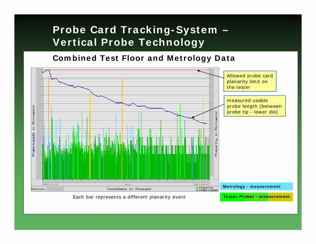
Probe Card Tracking-System –Vertical Probe TechnologyCombined Test Floor and Metrology Data
Metrology - measurement
Tester-Prober - measurement
measured usable probe length (between probe tip - lower die)
Allowed probe card planarity limit on the tester
Each bar represents a different planarity event

13-June-2006 SWTW – Probe Metrology Panel10
Probe Card Tracking-System –Vertical Probe Technology
signal probe planarity
Metrology Data

13-June-2006 SWTW – Probe Metrology Panel11
Probe Card Tracking-System –Cantilever Probe Technology
Combined Test Floor and Metrology Data

Probe Metrology Panel
Southwest Test Workshop 2006
Ger Koch

Semiconductors, IMO Ger Koch, June 2006 2
1. Philips Semiconductor, introduction
1.1 Sites, how organized
1.2 Key figures
1.3 FPC technologies
2. Probecard tracking
3. Metrology methods
4. Metrology examples
5. Trends & Issues
Contents

Semiconductors, IMO Ger Koch, June 2006 3
• It combines both Foundry (Front-End) and Assembly & Test (Back-End) capabilities into one integrated manufacturing organization.
• Manufacturing sites in Asia, Europe and United States.
1. IC Manufacturing Organization (IMO)

Semiconductors, IMO Ger Koch, June 2006 4
Cabuyao
Calamba
= Front-End
= Back-End
Caen
Eindhoven
Hamburg
KaohsiungBangkok
Suzhou
Singapore
= Head Office
FishkillBoeblingen
Crolles
Nijmegen
1.1 IMO Sites

Semiconductors, IMO Ger Koch, June 2006 5
1.1 IMO international co-operation modelWithin the IMO test department, relevant for Probe processes:
• Prober User Group
• Hardware Standardization Group
• Fab Automation Group
• standardization of probe processes, incl. prober platforms.
• Knowledge sharing
• Shop floor control (incl. wafermap handling)
• Test data management
Co-operation between disciplines is key!

Semiconductors, IMO Ger Koch, June 2006 6
• Supporting production of over 40k wafers/wk (4” - 12”)• IC’s & discrete
– Everything but “pentiums” & stand alone memory• Processes: CMOS down to 0.09, Bipolar, Bi-, BCDMOS, QUBIC, ‘++’• Total number of probers: over 650
– Prober platforms:• EG & TSK• Mostly ambient & Hot, some tri-temp
• Total number of testers: over 1500– Test platforms: Agilent, Credence, LTX, Philips, Spea, Teradyne
• Test environment:– General BE: Class 10000, Cleanroom: Class 1000
• Over 15.000 probecards in inventory• Over 2000 active products
1.2 Key figures

Semiconductors, IMO Ger Koch, June 2006 7
• Probecard Technologies: – 88% Cantilever (epoxy & blades)
• internal & external designs and (re)build– 10% Vertical
• Vendor design– 2% other (membrane)
• Internal & external design and (re)build
• Cleaning:– on-line: 1um & 3um AlOx. Cleaning interval: 100-300 touchdowns– off-line: chemical cleaning, sand paper, brush
• Preventive maintenance (avg 100k TD)
1.3 Probecards

Semiconductors, IMO Ger Koch, June 2006 8
2. Probecard tracking system• Integral part of Shop Floor Control system
• Key tracking parameters:– # touch downs– repair history– location– cleaning method

Semiconductors, IMO Ger Koch, June 2006 9
3. Metrology methodsApplied methods vary per site and per technology
• Tip diameter increase triggers P.M. re-shaping, repair (change spider)
• TD monitoring
• PCA check after each off line cleaning stage– planarity– x, y accuracy– tip diameter– Cres, leakage, PCB components
• Retest Recovery monitoring

Semiconductors, IMO Ger Koch, June 2006 10
Rx are monitored for all wafers for all probers.
Rx data used for:
• Direct feedback towards the operators (“MIT: Map in Time” system)
• Engineering purposes to prove effectiveness of process improvements
Next steps:
1. Online Cres monitoring (real SPC!)
2. Apply “smart” post processing techniques, to optimize the integral test process (incl. but not limited to probing only)
4.1 MiT, Retest Recovery monitoring

Semiconductors, IMO Ger Koch, June 2006 11
"on-the-fly“ actions, based on MiT
Diagnosis by system ( Production + RM )
Call out for support
Product Engineering
Problem List
Process Engineering
System Engineering Type
Engineering
Production SOP check
Diary Review Meeting

Semiconductors, IMO Ger Koch, June 2006 12
90
92
94
96
98
100
516 518 520 522 524 526 528 530 532 534 536 538 540 542 544 546 548 550 552
Effect of MIT on tester utilization
MiT implemented

Semiconductors, IMO Ger Koch, June 2006 13
Rx reduction, replacing (vertical) probes
RRR
RR
Retest Recovery monitoring

Semiconductors, IMO Ger Koch, June 2006 14
needle tip diameter increase
0
5
10
15
20
1 2 3 4 5 6 7 8 9
touchdowns
tip d
iam
eter
Needle tip re-shaping by prolonged z-only cleaning on special foil
For flat and semi-round!
Small tip Large tip
wear
reshape
4.2 Tip diameter

Semiconductors, IMO Ger Koch, June 2006 15
5. Trends and Issues• Low-k & Pad on Active dictate low gram forces, high planarity• Trends in:
– Pitch/padsize, Temperature, Current, Frequency, …….• Cres conditioning• Vendor probecard leadtime versus TpT waferfab• Tracking of separate heads, PCB’s etc• Probecards become “loadboards”
OK, we can probe this product, “but”If Temp<85 deg C
If current <250 mAIf Freq. < 1 gHz
If …


Qimonda · Frank Pietzschmann QD CTD BE WT 2006-06-13 · Page 1
Production 300
Office Buildings
RDC
Support & Backend
Bird View Qimonda Dresden/Germany
Qimonda QimondaInfineon
Production 200
Probe Metrology Panel

Qimonda · Frank Pietzschmann QD CTD BE WT 2006-06-13 · Page 2
Probe Facility- Supports total output of 12” Pilot Fab & 8” Fab- WSPW: 7.200 300mm, 6.000 200mm & 6.000 200mm (production & development)- Technologies: 110nm, 90nm, 70nm, 60nm, 50nm and beyond- DRAM, graphic RAM, Flash up to 1GB (~25 products), ~5 Test chips & Logic (~20 products), Smart card ( ~45 products), ~15 Test chips
- standard test flow, KGD, RDL, -10°C… 127°C- 3.700 Square Meter, Class 1000 clean room- 120 Operators on 4 shifts for 24/7 - 2 Probe card Techs (Repair) + 1 Eng (Incoming inspection) normal shift- 1 Probe card Tech per shift for cleaning & analysis- 1 Supervisor & 3 Techs per shift, 10 Probe Engrs & 5 Probe Engrs n. shift- Tester: ADVANTEST 8x T5365, 30x T5571, 8x T5771, 16x T5375, 17x HP4072Teradyne 19x J750, 1x Catalyst, 3x J971, 10x SPEA, 1x A93K, 13x HP4072
- Prober: ~120x Accretech AP-M-90 … UF3000, 6x TEL P8 Infineon

Qimonda · Frank Pietzschmann QD CTD BE WT 2006-06-13 · Page 3
Probe Cards
New Probe cards sorted by Technology 2004 (compared to 2003)
Cantilever
MEMS
Vertical
others
~100x 300mm, 300x 200mm active probe cards Memory & ~450 logic probe cards

Qimonda · Frank Pietzschmann QD CTD BE WT 2006-06-13 · Page 4
Probe Card Repair
Burned TipBurned Tip
Bent TipBent Tip
Card history check
Missing TipMissing Tip
Dependency on:- Temperature- LoadFailure located at:- PCB- Interconnector- Probe head
Cleaning Optical InspectionOptical Inspection
Probe card related contact fails
PCB InspectionPCB Inspection
ZIF connectorZIF connector
Pogo pin padPogo pin pad
WiringWiring
Tip InspectionTip Inspection
new failurenew failure repeated failurerepeated failure
Electrical Inspection
Grid arrayGrid array
1.
5.
4. 3.
2.if
no ro
ot c
ause
foun
d
90%90% 10%10%
failure verifying
ParticleParticle
Formularized maintenance flows

Qimonda · Frank Pietzschmann QD CTD BE WT 2006-06-13 · Page 5
Probe Card Tracking
Touchdown counter
Probe card Inspection
Online performance observation
Probe mark inspection
Probe card tracking system
Prober logging system
status, history
touchdowns, cleaning touchdowns
tip position, -size, pictures
probing process parameter, rejected chips, number of manual reviews
PMI stops, alignment errors
Cres or yield of a Cres sensible test
re-measurement rateLot tracking system
Increased Importance
Trigger for cleaning, end of live Trigger for repairInputs for measurement program Input for capacity planningPC vendor quality feedback, Probing process feedbackTask manager, ...
Oracle database with web-application
Probe card IdentificationAuto ID, storage

Qimonda · Frank Pietzschmann QD CTD BE WT 2006-06-13 · Page 6
Probe Card Cleaning
Cres online control PE softwareWafer test tool
Smart cleaning trigger is a must
…but check the scrubs marks before
bad scrub –missing overdrive
scrub mark tip

Qimonda · Frank Pietzschmann QD CTD BE WT 2006-06-13 · Page 7
Probe Card Metrology System
probe card & wafer inspection systemprobing process analysisprobe card repair
Advanced Probing Process Analyzer
- significant reduction of incoming inspection time for LAA probe cards
- offset/scaling assessment (manufacturing & temperature related;fast response to the manufacturer)
- Probing process assessment (process window, equipment, setup, …)
- fast root cause analysis for performance issues
- fast tip (automated) inspection (incoming/ wear control)
- Cleaning optimization
- Check of backend requirements ( pad damage; scrub hill, exposedoxide)
- Particle on wafer assessment (is a particle critical for the probe card?)
- Probing process developments (thinner alu, rerouting, bumps, lessprobing particles, contact on Au,…)
- “little” repairs (beam adjustments, single needle cleaning)
Tasks for the inspection tool sorted by importance
The biggest strategy change

Qimonda · Frank Pietzschmann QD CTD BE WT 2006-06-13 · Page 8
Probe Card Metrology System
worst case min. distance end of scrub to pad edge right: 7,3um
… saves dramatically incoming inspection time
Scan time: 7minfor a full probed 300mm wafer
Scan time: 27minfor ~ 200.000 pads on 200mm wafer
The power of systematic scrub mark analysis …

Qimonda · Frank Pietzschmann QD CTD BE WT 2006-06-13 · Page 9
Probe Card Metrology System
#10#01
diff. btw. left/right wafer half ~7um
X-movement ~7umafter 4h
quality control after new prober setup
diff. btw. left/right probe array side~5um
diff. btw. 1st/3rd touchdown ~4um
proberprobe card
wafer load
X-drift
… gives you valuable hints for probing process optimization
The power of systematic scrub mark analysis …

Qimonda · Frank Pietzschmann QD CTD BE WT 2006-06-13 · Page 10
Probe Card Metrology System
The power of systematic scrub mark analysis …
typical pattern “chuck with loose screws”
up to 10um increased end of scrub distanceto the pad edge after maintenance
Scrub x/y- position vector view
Screws for chuck fixing
Screws getting loose due totemperature change & probing force
… will increase your yield!