Embed Size (px)
Citation preview
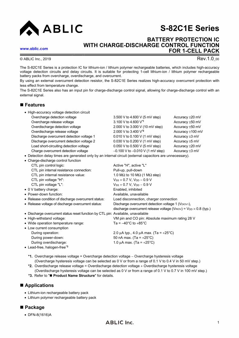
S-82C1E SeriesBATTERY PROTECTION IC
WITH CHARGE-DISCHARGE CONTROL FUNCTIONFOR 1-CELL PACKwww.ablic.com
© ABLIC Inc., 2019 Rev.1.0_00
1
The S-82C1E Series is a protection IC for lithium-ion / lithium polymer rechargeable batteries, which includes high-accuracy voltage detection circuits and delay circuits. It is suitable for protecting 1-cell lithium-ion / lithium polymer rechargeable battery packs from overcharge, overdischarge, and overcurrent. By using an external overcurrent detection resistor, the S-82C1E Series realizes high-accuracy overcurrent protection with less effect from temperature change. The S-82C1E Series also has an input pin for charge-discharge control signal, allowing for charge-discharge control with an external signal. Features
• High-accuracy voltage detection circuit Overcharge detection voltage 3.500 V to 4.600 V (5 mV step) Accuracy ±20 mV Overcharge release voltage 3.100 V to 4.600 V*1 Accuracy ±50 mV Overdischarge detection voltage 2.000 V to 3.000 V (10 mV step) Accuracy ±50 mV Overdischarge release voltage 2.000 V to 3.400 V*2 Accuracy ±100 mV Discharge overcurrent detection voltage 1 0.010 V to 0.100 V (1 mV step) Accuracy ±3 mV Discharge overcurrent detection voltage 2 0.030 V to 0.200 V (1 mV step) Accuracy ±5 mV Load short-circuiting detection voltage 0.050 V to 0.500 V (5 mV step) Accuracy ±20 mV Charge overcurrent detection voltage −0.100 V to −0.010 V (1 mV step) Accuracy ±3 mV • Detection delay times are generated only by an internal circuit (external capacitors are unnecessary). • Charge-discharge control function CTL pin control logic: Active "H", active "L" CTL pin internal resistance connection: Pull-up, pull-down CTL pin internal resistance value: 1.0 MΩ to 10 MΩ (1 MΩ step) CTL pin voltage "H": VSS + 0.7 V, VDD − 0.9 V CTL pin voltage "L": VSS + 0.7 V, VDD − 0.9 V • 0 V battery charge: Enabled, inhibited • Power-down function: Available, unavailable • Release condition of discharge overcurrent status: Load disconnection, charger connection • Release voltage of discharge overcurrent status: Discharge overcurrent detection voltage 1 (VDIOV1), discharge overcurrent release voltage (VRIOV) = VDD × 0.8 (typ.) • Discharge overcurrent status reset function by CTL pin: Available, unavailable • High-withstand voltage: VM pin and CO pin: Absolute maximum rating 28 V • Wide operation temperature range: Ta = −40°C to +85°C • Low current consumption During operation: 2.0 μA typ., 4.0 μA max. (Ta = +25°C) During power-down: 50 nA max. (Ta = +25°C) During overdischarge: 1.0 μA max. (Ta = +25°C) • Lead-free, halogen-free P
*3
*1. Overcharge release voltage = Overcharge detection voltage − Overcharge hysteresis voltage (Overcharge hysteresis voltage can be selected as 0 V or from a range of 0.1 V to 0.4 V in 50 mV step.)
*2. Overdischarge release voltage = Overdischarge detection voltage + Overdischarge hysteresis voltage (Overdischarge hysteresis voltage can be selected as 0 V or from a range of 0.1 V to 0.7 V in 100 mV step.)
*3. Refer to " Product Name Structure" for details. Applications
• Lithium-ion rechargeable battery pack • Lithium polymer rechargeable battery pack
Package
• DFN-8(1616)A

BATTERY PROTECTION IC WITH CHARGE-DISCHARGE CONTROL FUNCTION FOR 1-CELL PACK S-82C1E Series Rev.1.0_00
2
Block Diagram
Control logic
Delay circuit
Oscillator
VINI
VSS
VDD
CO
DO
VM
CTL
Overdischarge detection comparator
Overcharge detection comparator
Discharge overcurrent detection 1 comparator
Discharge overcurrent detection 2 comparator
Load short-circuiting detection comparator
Charge overcurrent detection comparator
Pull-up / pull-down selection circuit
Figure 1

BATTERY PROTECTION IC WITH CHARGE-DISCHARGE CONTROL FUNCTION FOR 1-CELL PACK Rev.1.0_00 S-82C1E Series
3
Product Name Structure
1. Product name
S-82C1E xx - A8T6 S
Package abbreviation and IC packing specifications*1 A8T6: DFN-8(1616)A, Tape
Serial code
Environmental code S: Lead-free, halogen-free
*1. Refer to the tape drawing.
2. Package Table 1 Package Drawing Codes
Package Name Dimension Tape Reel Land DFN-8(1616)A PW008-A-P-SD PW008-A-C-SD PW008-A-R-SD PW008-A-L-SD
BATTERY PROTECTION IC WITH CHARGE-DISCHARGE CONTROL FUNCTION FOR 1-CELL PACK S-82C1E Series Rev.1.0_00
4
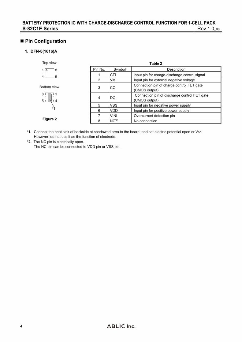
Pin Configuration
1. DFN-8(1616)A
Top view
1 8
4 5
Bottom view
8 1
5 4
*1
Figure 2
Table 2
Pin No. Symbol Description 1 CTL Input pin for charge-discharge control signal 2 VM Input pin for external negative voltage
3 CO Connection pin of charge control FET gate (CMOS output)
4 DO Connection pin of discharge control FET gate (CMOS output)
5 VSS Input pin for negative power supply 6 VDD Input pin for positive power supply 7 VINI Overcurrent detection pin 8 NC*2 No connection
*1. Connect the heat sink of backside at shadowed area to the board, and set electric potential open or VDD.
However, do not use it as the function of electrode. *2. The NC pin is electrically open.
The NC pin can be connected to VDD pin or VSS pin.
BATTERY PROTECTION IC WITH CHARGE-DISCHARGE CONTROL FUNCTION FOR 1-CELL PACK Rev.1.0_00 S-82C1E Series
5
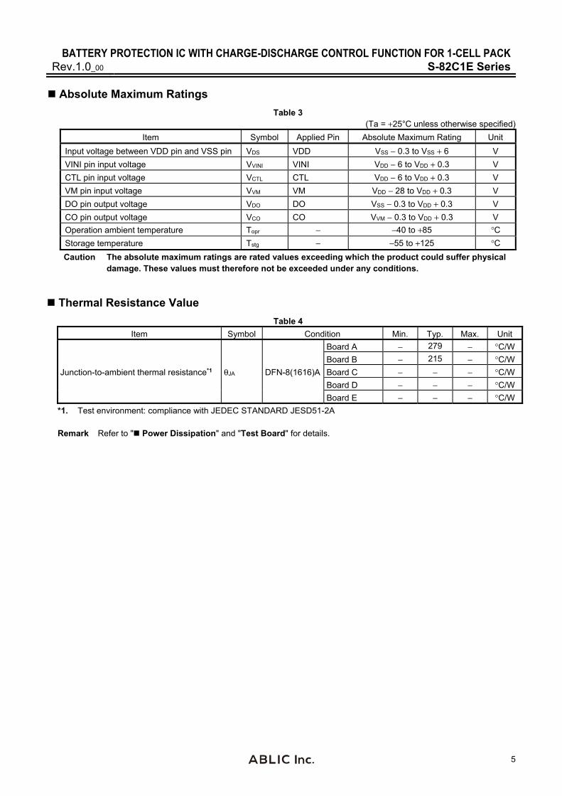
Absolute Maximum Ratings Table 3
(Ta = +25°C unless otherwise specified)Item Symbol Applied Pin Absolute Maximum Rating Unit
Input voltage between VDD pin and VSS pin VDS VDD VSS − 0.3 to VSS + 6 V VINI pin input voltage VVINI VINI VDD − 6 to VDD + 0.3 V CTL pin input voltage VCTL CTL VDD − 6 to VDD + 0.3 V VM pin input voltage VVM VM VDD − 28 to VDD + 0.3 V DO pin output voltage VDO DO VSS − 0.3 to VDD + 0.3 V CO pin output voltage VCO CO VVM − 0.3 to VDD + 0.3 V Operation ambient temperature Topr − −40 to +85 °C Storage temperature Tstg − −55 to +125 °C Caution The absolute maximum ratings are rated values exceeding which the product could suffer physical
damage. These values must therefore not be exceeded under any conditions. Thermal Resistance Value
Table 4 Item Symbol Condition Min. Typ. Max. Unit
Junction-to-ambient thermal resistance*1 θJA DFN-8(1616)A
Board A − 279 − °C/W Board B − 215 − °C/W Board C − − − °C/W Board D − − − °C/W Board E − − − °C/W
*1. Test environment: compliance with JEDEC STANDARD JESD51-2A Remark Refer to " Power Dissipation" and "Test Board" for details.

BATTERY PROTECTION IC WITH CHARGE-DISCHARGE CONTROL FUNCTION FOR 1-CELL PACK S-82C1E Series Rev.1.0_00
6
Electrical Characteristics
1. Ta = +25°C Table 5
(Ta = +25°C unless otherwise specified)
Item Symbol Condition Min. Typ. Max. Unit Test Circuit
Detection Voltage Overcharge detection voltage VCU − VCU − 0.020 VCU VCU + 0.020 V 1
Overcharge release voltage VCL VCL ≠ VCU VCL − 0.050 VCL VCL + 0.050 V 1 VCL = VCU VCL − 0.025 VCL VCL + 0.020 V 1
Overdischarge detection voltage VDL − VDL − 0.050 VDL VDL + 0.050 V 2
Overdischarge release voltage VDU VDL ≠ VDU VDU − 0.100 VDU VDU + 0.100 V 2 VDL = VDU VDU − 0.050 VDU VDU + 0.050 V 2
Discharge overcurrent detection voltage 1 VDIOV1 − VDIOV1 − 0.003 VDIOV1 VDIOV1 + 0.003 V 2 Discharge overcurrent detection voltage 2 VDIOV2 − VDIOV2 − 0.005 VDIOV2 VDIOV2 + 0.005 V 2 Load short-circuiting detection voltage VSHORT − VSHORT − 0.020 VSHORT VSHORT + 0.020 V 2 Load short-circuiting detection voltage 2 VSHORT2 − VDD − 1.2 VDD − 0.8 VDD − 0.5 V 2 Charge overcurrent detection voltage VCIOV − VCIOV − 0.003 VCIOV VCIOV + 0.003 V 2 Discharge overcurrent release voltage VRIOV VDD = 3.4 V VDD × 0.77 VDD × 0.80 VDD × 0.83 V 2 0 V Battery Charge 0 V battery charge starting charger voltage V0CHA 0 V battery charge enabled 0.0 0.7 1.0 V 2 0 V battery charge inhibition battery voltage V0INH 0 V battery charge inhibited 0.9 1.2 1.5 V 2 Internal Resistance Resistance between VDD pin and VM pin RVMD VDD = 1.8 V, VVM = 0 V 500 1000 2000 kΩ 3 Resistance between VM pin and VSS pin RVMS VDD = 3.4 V, VVM = 1.0 V 5 10 15 kΩ 3 CTL pin internal resistance RCTL − RCTL × 0.5 RCTL RCTL × 2.0 MΩ 3 Input Voltage Operation voltage between VDD pin and VSS pin VDSOP1 − 1.5 − 6.0 V −
Operation voltage between VDD pin and VM pin VDSOP2 − 1.5 − 28 V −
CTL pin voltage "H" VCTLH − VCTLH − 0.3 VCTLH VCTLH + 0.3 V 2 CTL pin voltage "L" VCTLL − VCTLL − 0.3 VCTLL VCTLL + 0.3 V 2 Input Current Current consumption during operation IOPE VDD = 3.4 V, VVM = 0 V − 2.0 4.0 μA 3 Current consumption during power-down IPDN VDD = VVM = 1.5 V − − 0.05 μA 3 Current consumption during overdischarge IOPED VDD = VVM = 1.5 V − − 1.0 μA 3 Output Resistance CO pin resistance "H" RCOH − 5 10 20 kΩ 4 CO pin resistance "L" RCOL − 5 10 20 kΩ 4 DO pin resistance "H" RDOH − 5 10 20 kΩ 4 DO pin resistance "L" RDOL − 1 2 4 kΩ 4 Delay Time Overcharge detection delay time tCU − tCU × 0.7 tCU tCU × 1.3 − 5 Overdischarge detection delay time tDL − tDL × 0.7 tDL tDL × 1.3 − 5 Discharge overcurrent detection delay time 1 tDIOV1 − tDIOV1 × 0.75 tDIOV1 tDIOV1 × 1.25 − 5 Discharge overcurrent detection delay time 2 tDIOV2 − tDIOV2 × 0.7 tDIOV2 tDIOV2 × 1.3 − 5 Load short-circuiting detection delay time tSHORT − tSHORT × 0.7 tSHORT tSHORT × 1.3 − 5 Charge overcurrent detection delay time tCIOV − tCIOV × 0.7 tCIOV tCIOV × 1.3 − 5 Charge-discharge inhibition delay time tCTL − tCTL × 0.7 tCTL tCTL × 1.3 − 5

BATTERY PROTECTION IC WITH CHARGE-DISCHARGE CONTROL FUNCTION FOR 1-CELL PACK Rev.1.0_00 S-82C1E Series
7
2. Ta = −20°C to +60°C*1 Table 6
(Ta = −20°C to +60°C*1 unless otherwise specified)
Item Symbol Condition Min. Typ. Max. Unit Test Circuit
Detection Voltage Overcharge detection voltage VCU − VCU − 0.025 VCU VCU + 0.025 V 1
Overcharge release voltage VCL VCL ≠ VCU VCL − 0.065 VCL VCL + 0.057 V 1 VCL = VCU VCL − 0.030 VCL VCL + 0.025 V 1
Overdischarge detection voltage VDL − VDL − 0.060 VDL VDL + 0.055 V 2
Overdischarge release voltage VDU VDL ≠ VDU VDU − 0.110 VDU VDU + 0.105 V 2 VDL = VDU VDU − 0.060 VDU VDU + 0.055 V 2
Discharge overcurrent detection voltage 1 VDIOV1 − VDIOV1 − 0.003 VDIOV1 VDIOV1 + 0.003 V 2 Discharge overcurrent detection voltage 2 VDIOV2 − VDIOV2 − 0.005 VDIOV2 VDIOV2 + 0.005 V 2 Load short-circuiting detection voltage VSHORT − VSHORT − 0.020 VSHORT VSHORT + 0.020 V 2 Load short-circuiting detection voltage 2 VSHORT2 − VDD − 1.4 VDD − 0.8 VDD − 0.3 V 2 Charge overcurrent detection voltage VCIOV − VCIOV − 0.003 VCIOV VCIOV + 0.003 V 2 Discharge overcurrent release voltage VRIOV VDD = 3.4 V VDD × 0.77 VDD × 0.80 VDD × 0.83 V 2 0 V Battery Charge 0 V battery charge starting charger voltage V0CHA 0 V battery charge enabled 0.0 0.7 1.5 V 2 0 V battery charge inhibition battery voltage V0INH 0 V battery charge inhibited 0.7 1.2 1.7 V 2 Internal Resistance Resistance between VDD pin and VM pin RVMD VDD = 1.8 V, VVM = 0 V 250 1000 3000 kΩ 3 Resistance between VM pin and VSS pin RVMS VDD = 3.4 V, VVM = 1.0 V 3.5 10 20 kΩ 3 CTL pin internal resistance RCTL − RCTL × 0.25 RCTL RCTL × 3.0 MΩ 3 Input Voltage Operation voltage between VDD pin and VSS pin
VDSOP1 − 1.5 − 6.0 V −
Operation voltage between VDD pin and VM pin
VDSOP2 − 1.5 − 28 V −
CTL pin voltage "H" VCTLH − VCTLH − 0.4 VCTLH VCTLH + 0.4 V 2 CTL pin voltage "L" VCTLL − VCTLL − 0.4 VCTLL VCTLL + 0.4 V 2 Input Current Current consumption during operation IOPE VDD = 3.4 V, VVM = 0 V − 2.0 5.0 μA 3 Current consumption during power-down IPDN VDD = VVM = 1.5 V − − 0.1 μA 3 Current consumption during overdischarge IOPED VDD = VVM = 1.5 V − − 1.5 μA 3 Output Resistance CO pin resistance "H" RCOH − 2.5 10 30 kΩ 4 CO pin resistance "L" RCOL − 2.5 10 30 kΩ 4 DO pin resistance "H" RDOH − 2.5 10 30 kΩ 4 DO pin resistance "L" RDOL − 0.5 2 6 kΩ 4 Delay Time Overcharge detection delay time tCU − tCU × 0.6 tCU tCU × 1.4 − 5 Overdischarge detection delay time tDL − tDL × 0.6 tDL tDL × 1.4 − 5 Discharge overcurrent detection delay time 1 tDIOV1 − tDIOV1 × 0.65 tDIOV1 tDIOV1 × 1.35 − 5 Discharge overcurrent detection delay time 2 tDIOV2 − tDIOV2 × 0.6 tDIOV2 tDIOV2 × 1.4 − 5 Load short-circuiting detection delay time tSHORT − tSHORT × 0.6 tSHORT tSHORT × 1.4 − 5 Charge overcurrent detection delay time tCIOV − tCIOV × 0.6 tCIOV tCIOV × 1.4 − 5 Charge-discharge inhibition delay time tCTL − tCTL × 0.6 tCTL tCTL × 1.4 − 5 *1. Since products are not screened at high and low temperature, the specification for this temperature range is guaranteed
by design, not tested in production.

BATTERY PROTECTION IC WITH CHARGE-DISCHARGE CONTROL FUNCTION FOR 1-CELL PACK S-82C1E Series Rev.1.0_00
8
3. Ta = −40°C to +85°C*1 Table 7
(Ta = −40°C to +85°C*1 unless otherwise specified)
Item Symbol Condition Min. Typ. Max. Unit Test Circuit
Detection Voltage Overcharge detection voltage VCU − VCU − 0.045 VCU VCU + 0.030 V 1
Overcharge release voltage VCL VCL ≠ VCU VCL − 0.080 VCL VCL + 0.060 V 1 VCL = VCU VCL − 0.050 VCL VCL + 0.030 V 1
Overdischarge detection voltage VDL − VDL − 0.080 VDL VDL + 0.060 V 2
Overdischarge release voltage VDU VDL ≠ VDU VDU − 0.130 VDU VDU + 0.110 V 2 VDL = VDU VDU − 0.080 VDU VDU + 0.060 V 2
Discharge overcurrent detection voltage 1 VDIOV1 − VDIOV1 − 0.003 VDIOV1 VDIOV1 + 0.003 V 2 Discharge overcurrent detection voltage 2 VDIOV2 − VDIOV2 − 0.005 VDIOV2 VDIOV2 + 0.005 V 2 Load short-circuiting detection voltage VSHORT − VSHORT − 0.020 VSHORT VSHORT + 0.020 V 2 Load short-circuiting detection voltage 2 VSHORT2 − VDD − 1.4 VDD − 0.8 VDD − 0.3 V 2 Charge overcurrent detection voltage VCIOV − VCIOV − 0.003 VCIOV VCIOV + 0.003 V 2 Discharge overcurrent release voltage VRIOV VDD = 3.4 V VDD × 0.77 VDD × 0.80 VDD × 0.83 V 2 0 V Battery Charge 0 V battery charge starting charger voltage V0CHA 0 V battery charge enabled 0.0 0.7 1.5 V 2 0 V battery charge inhibition battery voltage V0INH 0 V battery charge inhibited 0.7 1.2 1.7 V 2 Internal Resistance Resistance between VDD pin and VM pin RVMD VDD = 1.8 V, VVM = 0 V 250 1000 3000 kΩ 3 Resistance between VM pin and VSS pin RVMS VDD = 3.4 V, VVM = 1.0 V 3.5 10 20 kΩ 3 CTL pin internal resistance RCTL − RCTL × 0.25 RCTL RCTL × 3.0 MΩ 3 Input Voltage Operation voltage between VDD pin and VSS pin
VDSOP1 − 1.5 − 6.0 V −
Operation voltage between VDD pin and VM pin
VDSOP2 − 1.5 − 28 V −
CTL pin voltage "H" VCTLH − VCTLH − 0.4 VCTLH VCTLH + 0.4 V 2 CTL pin voltage "L" VCTLL − VCTLL − 0.4 VCTLL VCTLL + 0.4 V 2 Input Current Current consumption during operation IOPE VDD = 3.4 V, VVM = 0 V − 2.0 5.0 μA 3 Current consumption during power-down IPDN VDD = VVM = 1.5 V − − 0.1 μA 3 Current consumption during overdischarge IOPED VDD = VVM = 1.5 V − − 1.5 μA 3 Output Resistance CO pin resistance "H" RCOH − 2.5 10 30 kΩ 4 CO pin resistance "L" RCOL − 2.5 10 30 kΩ 4 DO pin resistance "H" RDOH − 2.5 10 30 kΩ 4 DO pin resistance "L" RDOL − 0.5 2 6 kΩ 4 Delay Time Overcharge detection delay time tCU − tCU × 0.4 tCU tCU × 1.6 − 5 Overdischarge detection delay time tDL − tDL × 0.4 tDL tDL × 1.6 − 5 Discharge overcurrent detection delay time 1 tDIOV1 − tDIOV1 × 0.4 tDIOV1 tDIOV1 × 1.6 − 5 Discharge overcurrent detection delay time 2 tDIOV2 − tDIOV2 × 0.4 tDIOV2 tDIOV2 × 1.6 − 5 Load short-circuiting detection delay time tSHORT − tSHORT × 0.4 tSHORT tSHORT × 1.6 − 5 Charge overcurrent detection delay time tCIOV − tCIOV × 0.4 tCIOV tCIOV × 1.6 − 5 Charge-discharge inhibition delay time tCTL − tCTL × 0.4 tCTL tCTL × 1.6 − 5 *1. Since products are not screened at high and low temperature, the specification for this temperature range is guaranteed
by design, not tested in production.
BATTERY PROTECTION IC WITH CHARGE-DISCHARGE CONTROL FUNCTION FOR 1-CELL PACK Rev.1.0_00 S-82C1E Series
9
Test Circuits When CTL pin control logic is active "H", SW1 and SW3 are turned off, SW2 and SW4 are turned on. When CTL pin control logic is active "L", SW1 and SW3 are turned on, SW2 and SW4 are turned off. Caution Unless otherwise specified, the output voltage levels "H" and "L" at CO pin (VCO) and DO pin (VDO) are
judged by the threshold voltage (1.0 V) of the N-channel FET. Judge the CO pin level with respect to VVM and the DO pin level with respect to VSS.
1. Overcharge detection voltage, overcharge release voltage
(Test circuit 1)
Overcharge detection voltage (VCU) is defined as the voltage V1 at which VCO goes from "H" to "L" when the voltage V1 is gradually increased from the starting condition of V1 = 3.4 V. Overcharge release voltage (VCL) is defined as the voltage V1 at which VCO goes from "L" to "H" when the voltage V1 is then gradually decreased. Overcharge hysteresis voltage (VHC) is defined as the difference between VCU and VCL.
2. Overdischarge detection voltage, overdischarge release voltage
(Test circuit 2)
Overdischarge detection voltage (VDL) is defined as the voltage V1 at which VDO goes from "H" to "L" when the voltage V1 is gradually decreased from the starting conditions of V1 = 3.4 V, V2 = V5 = V6 = 0 V. Overdischarge release voltage (VDU) is defined as the voltage V1 at which VDO goes from "L" to "H" when setting V2 = 0.01 V, V5 = V6 = 0 V and when the voltage V1 is then gradually increased. Overdischarge hysteresis voltage (VHD) is defined as the difference between VDU and VDL.
3. Discharge overcurrent detection voltage 1, discharge overcurrent release voltage
(Test circuit 2)
3. 1 Release voltage of discharge overcurrent status "VDIOV1"
Discharge overcurrent detection voltage 1 (VDIOV1) is defined as the voltage V5 whose delay time for changing VDO from "H" to "L" is discharge overcurrent detection delay time 1 (tDIOV1) when the voltage V5 is increased from the starting conditions of V1 = 3.4 V, V2 = 1.4 V, V5 = V6 = 0 V. VDO goes from "L" to "H" when setting V2 = 3.4 V, V5 = 0 V and when the voltage V2 is then gradually decreased to VDIOV1 typ. or lower.
3. 2 Release voltage of discharge overcurrent status "VRIOV"
VDIOV1 is defined as the voltage V5 whose delay time for changing VDO from "H" to "L" is tDIOV1 when the voltage V5 is increased from the starting conditions of V1 = 3.4 V, V2 = 1.4 V, V5 = V6 = 0 V. Discharge overcurrent release voltage (VRIOV) is defined as the voltage V2 at which VDO goes from "L" to "H" when setting V2 = 3.4 V, V5 = 0 V and when the voltage V2 is then gradually decreased.
4. Discharge overcurrent detection voltage 2
(Test circuit 2)
Discharge overcurrent detection voltage 2 (VDIOV2) is defined as the voltage V5 whose delay time for changing VDO from "H" to "L" is discharge overcurrent detection delay time 2 (tDIOV2) when the voltage V5 is increased from the starting conditions of V1 = 3.4 V, V2 = 1.4 V, V5 = V6 = 0 V.
5. Load short-circuiting detection voltage
(Test circuit 2)
Load short-circuiting detection voltage (VSHORT) is defined as the voltage V5 whose delay time for changing VDO from "H" to "L" is load short-circuiting detection delay time (tSHORT) when the voltage V5 is increased from the starting conditions of V1 = 3.4 V, V2 = 1.4 V, V5 = V6 = 0 V.
6. Load shorting-circuiting detection voltage 2
(Test circuit 2)
Load short-circuiting detection voltage 2 (VSHORT2) is defined as the voltage V2 whose delay time for changing VDO from "H" to "L" is tSHORT when the voltage V2 is increased from the starting conditions of V1 = 3.4 V, V2 = V5 = V6 = 0 V.
BATTERY PROTECTION IC WITH CHARGE-DISCHARGE CONTROL FUNCTION FOR 1-CELL PACK S-82C1E Series Rev.1.0_00
10
7. Charge overcurrent detection voltage
(Test circuit 2)
Charge overcurrent detection voltage (VCIOV) is defined as the voltage V5 whose delay time for changing VCO from "H" to "L" is charge overcurrent detection delay time (tCIOV) when the voltage V5 is decreased from the starting conditions of V1 = 3.4 V, V2 = V5 = V6 = 0 V.
8. CTL pin voltage "H", CTL pin voltage "L" (Test circuit 2)
8. 1 CTL pin control logic active "H"
The CTL pin voltage "H" (VCTLH) is defined as the voltage V6 at which VCO and VDO go from "H" to "L" and when the voltage V6 is gradually increased under the set conditions of V1 = 3.4 V, V2 = V5 = V6 = 0 V. After that, the CTL pin voltage "L" (VCTLL) is defined as the voltage V6 at which VCO and VDO go from "L" to "H" after V6 is gradually decreased.
8. 2 CTL pin control logic active "L"
The CTL pin voltage "L" (VCTLL) is defined as the voltage difference between the voltage V6 and the voltage V1 (V1 − V6) at which VCO and VDO go from "H" to "L" when the voltage V6 is gradually increased under the set conditions of V1 = 3.4 V, V2 = V5 = V6 = 0 V. After that, the CTL pin voltage "H" (VCTLH) is defined as the voltage difference between V1 − V6 at which VCO and VDO go from "L" to "H" after V6 is gradually decreased.
9. Current consumption during operation (Test circuit 3)
The current consumption during operation (IOPE) is the current that flows through the VDD pin (IDD) under the set conditions of V1 = 3.4 V and V2 = V5 = V6 = 0 V. However, the current flowing through the internal resistor of the CTL pin is excluded.
10. Current consumption during power-down, current consumption during overdischarge
(Test circuit 3)
10. 1 With power-down function
The current consumption during power-down (IPDN) is IDD under the set conditions of V1 = V2 = 1.5 V, V5 = V6 = 0 V.
10. 2 Without power-down function
The current consumption during overdischarge (IOPED) is IDD under the set conditions of V1 = V2 = 1.5 V, V5 = V6 = 0 V.
11. Resistance between VDD pin and VM pin (Test circuit 3)
RVMD is the resistance between VDD pin and VM pin under the set conditions of V1 = 1.8 V, V2 = V5 = V6 = 0 V.
12. Resistance between VM pin and VSS pin (Release condition of discharge overcurrent status "load disconnection") (Test circuit 3)
RVMS is the resistance between VM pin and VSS pin when the voltage V5 is decreased to 0 V from the starting conditions of V1 = 3.4 V, V2 = V5 = 1.0 V, V6 = 0 V.

BATTERY PROTECTION IC WITH CHARGE-DISCHARGE CONTROL FUNCTION FOR 1-CELL PACK Rev.1.0_00 S-82C1E Series
11
13. CTL pin internal resistance (Test circuit 3)
13. 1 CTL pin control logic active "H" and CTL pin internal resistance connection "pull-up"
The CTL pin internal resistance (RCTL) is the resistance between CTL pin and VDD pin under the set conditions of V1 = 3.4 V, V2 = V5 = V6 = 0 V.
13. 2 CTL pin control logic active "H" and CTL pin internal resistance connection "pull-down"
RCTL is the resistance between CTL pin and VSS pin under the set conditions of V1 = V6 = 3.4 V, V2 = V5 = 0 V.
13. 3 CTL pin control logic active "L" and CTL pin internal resistance connection "pull-up"
RCTL is the resistance between CTL pin and VDD pin under the set conditions of V1 = V6 = 3.4 V, V2 = V5 = 0 V.
13. 4 CTL pin control logic active "L" and CTL pin internal resistance connection "pull-down"
RCTL is the resistance between CTL pin and VSS pin under the set conditions of V1 = 3.4 V, V2 = V5 = V6 = 0 V.
14. CO pin resistance "H" (Test circuit 4)
The CO pin resistance "H" (RCOH) is the resistance between VDD pin and CO pin under the set conditions of V1 = 3.4 V, V2 = V5 = 0 V, V3 = 3.0 V.
15. CO pin resistance "L"
(Test circuit 4)
The CO pin resistance "L" (RCOL) is the resistance between VM pin and CO pin under the set conditions of V1 = 4.7 V, V2 = V5 = 0 V, V3 = 0.4 V.
16. DO pin resistance "H"
(Test circuit 4)
The DO pin resistance "H" (RDOH) is the resistance between VDD pin and DO pin under the set conditions of V1 = 3.4 V, V2 = V5 = 0 V, V4 = 3.0 V.
17. DO pin resistance "L"
(Test circuit 4)
The DO pin resistance "L" (RDOL) is the resistance between VSS pin and DO pin under the set conditions of V1 = 1.8 V, V2 = V5 = 0 V, V4 = 0.4 V.
18. Overcharge detection delay time
(Test circuit 5)
The overcharge detection delay time (tCU) is the time needed for VCO to go to "L" just after the voltage V1 increases and exceeds VCU under the set conditions of V1 = 3.4 V, V2 = V5 = V6 = 0 V.
19. Overdischarge detection delay time
(Test circuit 5)
The overdischarge detection delay time (tDL) is the time needed for VDO to go to "L" after the voltage V1 decreases and falls below VDL under the set conditions of V1 = 3.4 V, V2 = V5 = V6 = 0 V.
20. Discharge overcurrent detection delay time 1
(Test circuit 5)
The discharge overcurrent detection delay time 1 (tDIOV1) is the time needed for VDO to go to "L" after the voltage V5 increases and exceeds VDIOV1 under the set conditions of V1 = 3.4 V, V2 = 1.4 V, V5 = V6 = 0 V.
BATTERY PROTECTION IC WITH CHARGE-DISCHARGE CONTROL FUNCTION FOR 1-CELL PACK S-82C1E Series Rev.1.0_00
12
21. Discharge overcurrent detection delay time 2
(Test circuit 5)
The discharge overcurrent detection delay time 2 (tDIOV2) is the time needed for VDO to go to "L" after the voltage V5 increases and exceeds VDIOV2 under the set conditions of V1 = 3.4 V, V2 = 1.4 V, V5 = V6 = 0 V.
22. Load short-circuiting detection delay time
(Test circuit 5)
The load short-circuiting detection delay time (tSHORT) is the time needed for VDO to go to "L" after the voltage V5 increases and exceeds VSHORT under the set conditions of V1 = 3.4 V, V2 = 1.4 V, V5 = V6 = 0 V.
23. Charge overcurrent detection delay time
(Test circuit 5)
The charge overcurrent detection delay time (tCIOV) is the time needed for VCO to go to "L" after the voltage V5 decreases and falls below VCIOV under the set conditions of V1 = 3.4 V, V2 = V5 = V6 = 0 V.
24. Charge-discharge inhibition delay time
(Test circuit 5)
24. 1 CTL pin control logic active "H"
Charge-discharge inhibition delay time (tCTL) is the time needed for VCO and VDO to go to "L" after the voltage V6 increases and exceeds VCTLH under the set conditions of V1 = 3.4 V, V2 = V5 = V6 = 0 V.
24. 2 CTL pin control logic active "L"
Charge-discharge inhibition delay time (tCTL) is the time needed for VCO and VDO to go to "L" after the voltage V6 increases and V1 − V6 falls below VCTLL under the set conditions of V1 = 3.4 V, V2 = V5 = V6 = 0 V.
25. 0 V battery charge starting charger voltage (0 V battery charge enabled)
(Test circuit 2)
The 0 V battery charge starting charger voltage (V0CHA) is defined as the absolute value of voltage V2 at which VCO goes to "H" (VCO = VDD) when the voltage V2 is gradually decreased from the starting condition of V1 = V2 = V5 = V6 = 0 V.
26. 0 V battery charge inhibition battery voltage (0 V battery charge inhibited)
(Test circuit 2)
The 0 V battery charge inhibition battery voltage (V0INH) is defined as the voltage V1 at which VCO goes to "L" (VCO = VVM) when the voltage V1 is gradually decreased, after setting V1 = 1.8 V, V2 = −2.0 V, V5 = V6 = 0 V.

BATTERY PROTECTION IC WITH CHARGE-DISCHARGE CONTROL FUNCTION FOR 1-CELL PACK Rev.1.0_00 S-82C1E Series
13
V VDO V VCO
CO DO
VSS
SW1
VM
S-82C1E Series
R1 = 330 Ω
V1
COM
C1 = 0.1 μF
CTL SW2 VDD
VINI
V VDO V VCO
CO DO
VSS
VDD
VM
S-82C1E Series V1
V2
COM
CTL V6
SW1
SW2
SW4
SW3
VINI
V5
Figure 3 Test Circuit 1 Figure 4 Test Circuit 2
CO DO
VSS
VDD
VM
S-82C1E Series V1
V2
COM
A IDD
A IVM
ICTL CTL
V6
SW1
SW2
SW4
SW3
A
VINI
V5
A IDO A ICO
CO DO
VSS
VDD
VM
S-82C1E Series V1
V2
COM
V4 V3
CTL SW1
SW2
VINI
V5
Figure 5 Test Circuit 3 Figure 6 Test Circuit 4
CO DO
VSS
VDD
VM
S-82C1E Series V1
V2
COM
CTL V6
SW1
SW2
SW4
SW3
Oscilloscope Oscilloscope
VINI
V5
Figure 7 Test Circuit 5

BATTERY PROTECTION IC WITH CHARGE-DISCHARGE CONTROL FUNCTION FOR 1-CELL PACK S-82C1E Series Rev.1.0_00
14
Operation Remark Refer to " Battery Protection IC Connection Example". 1. Normal status
The S-82C1E Series monitors the voltage of the battery connected between VDD pin and VSS pin, the voltage between VINI pin and VSS pin and the voltage between CTL pin and VSS pin to control charging and discharging.
1. 1 CTL pin control logic active "H"
When the battery voltage is in the range from overdischarge detection voltage (VDL) to overcharge detection voltage (VCU), the VINI pin voltage is in the range from charge overcurrent detection voltage (VCIOV) to discharge overcurrent detection voltage 1 (VDIOV1), and the CTL pin voltage is equal to or lower than the CTL pin voltage "L" (VCTLL), the S-82C1E Series turns both the charge-discharge control FETs on. This condition is called the normal status, and in this condition charging and discharging can be carried out freely. The resistance between VDD pin and VM pin (RVMD), and the resistance between VM pin and VSS pin (RVMS) are not connected in the normal status.
1. 2 CTL pin control logic active "L"
When the battery voltage is in the range from overdischarge detection voltage (VDL) to overcharge detection voltage (VCU), the VINI pin voltage is in the range from charge overcurrent detection voltage (VCIOV) to discharge overcurrent detection voltage 1 (VDIOV1), and the CTL pin voltage is equal to or higher than the CTL pin voltage "H" (VCTLH), the S-82C1E Series turns both the charge-discharge control FETs on. This condition is called the normal status, and in this condition charging and discharging can be carried out freely. The resistance between VDD pin and VM pin (RVMD), and the resistance between VM pin and VSS pin (RVMS) are not connected in the normal status.
Caution After the battery is connected, discharging may not be carried out. In this case, the S-82C1E Series returns to the normal status by connecting a charger.
2. Overcharge status
2. 1 VCL ≠ VCU (Product in which overcharge release voltage differs from overcharge detection voltage) When the battery voltage becomes higher than VCU during charging in the normal status and the condition continues for the overcharge detection delay time (tCU) or longer, the S-82C1E Series turns the charge control FET off to stop charging. This condition is called the overcharge status. The overcharge status is released in the following two cases.
(1) In the case that the VM pin voltage is lower than 0.35 V typ., the S-82C1E Series releases the overcharge status when the battery voltage falls below overcharge release voltage (VCL).
(2) In the case that the VM pin voltage is equal to or higher than 0.35 V typ., the S-82C1E Series releases the overcharge status when the battery voltage falls below VCU.
When the discharge is started by connecting a load after the overcharge detection, the VM pin voltage rises by the Vf voltage of the parasitic diode than the VSS pin voltage, because the discharge current flows through the parasitic diode in the charge control FET. If this VM pin voltage is equal to or higher than 0.35 V typ., the S-82C1E Series releases the overcharge status when the battery voltage is equal to or lower than VCU.
Caution If the battery is charged to a voltage higher than VCU and the battery voltage does not fall below VCU even when a heavy load is connected, discharge overcurrent detection and load short-circuiting detection do not function until the battery voltage falls below VCU. Since an actual battery has an internal impedance of tens of mΩ, the battery voltage drops immediately after a heavy load that causes overcurrent is connected, and discharge overcurrent detection and load short-circuiting detection function.

BATTERY PROTECTION IC WITH CHARGE-DISCHARGE CONTROL FUNCTION FOR 1-CELL PACK Rev.1.0_00 S-82C1E Series
15
2. 2 VCL = VCU (Product in which overcharge release voltage is the same as overcharge detection voltage) When the battery voltage becomes higher than VCU during charging in the normal status and the condition continues for the overcharge detection delay time (tCU) or longer, the S-82C1E Series turns the charge control FET off to stop charging. This condition is called the overcharge status. In the case that the VM pin voltage is equal to or higher than 0.35 V typ. and the battery voltage falls below VCU, the S-82C1E Series releases the overcharge status. When the discharge is started by connecting a load after the overcharge detection, the VM pin voltage rises by the Vf voltage of the parasitic diode than the VSS pin voltage, because the discharge current flows through the parasitic diode in the charge control FET. If this VM pin voltage is equal to or higher than 0.35 V typ., the S-82C1E Series releases the overcharge status when the battery voltage is equal to or lower than VCU.
Caution 1. If the battery is charged to a voltage higher than VCU and the battery voltage does not fall below
VCU even when a heavy load is connected, discharge overcurrent detection and load short-circuiting detection do not function until the battery voltage falls below VCU. Since an actual battery has an internal impedance of tens of mΩ, the battery voltage drops immediately after a heavy load that causes overcurrent is connected, and discharge overcurrent detection and load short-circuiting detection function.
2. When a charger is connected after overcharge detection, the overcharge status is not released even if the battery voltage is below VCL. The overcharge status is released when the discharge current flows and the VM pin voltage goes over 0.35 V typ. by removing the charger.
3. Overdischarge status
When the battery voltage falls below VDL during discharging in the normal status and the condition continues for the overdischarge detection delay time (tDL) or longer, the S-82C1E Series turns the discharge control FET off to stop discharging. This condition is called the overdischarge status. Under the overdischarge status, VDD pin and VM pin are shorted by RVMD in the S-82C1E Series. The VM pin voltage is pulled up by RVMD. When connecting a charger in the overdischarge status, the battery voltage reaches VDL or higher and the S-82C1E Series releases the overdischarge status if the VM pin voltage falls below 0 V typ. The battery voltage reaches the overdischarge release voltage (VDU) or higher and the S-82C1E Series releases the overdischarge status if the VM pin voltage does not fall below 0 V typ. RVMS is not connected in the overdischarge status.
3. 1 With power-down function Under the overdischarge status, when voltage difference between VDD pin and VM pin is 0.8 V typ. or lower, the power-down function works and the current consumption is reduced to the current consumption during power-down (IPDN). By connecting a battery charger, the power-down function is released when the VM pin voltage is 0.7 V typ. or lower.
• When a battery is not connected to a charger and the VM pin voltage ≥ 0.7 V typ., the S-82C1E Seies maintains the overdischarge status even when the battery voltage reaches VDU or higher.
• When a battery is connected to a charger and 0.7 V typ. > the VM pin voltage > 0 V typ., the battery voltage reaches VDU or higher and the S-82C1E Series releases the overdischarge status.
• When a battery is connected to a charger and 0 V typ. ≥ the VM pin voltage, the battery voltage reaches VDL or higher and the S-82C1E Series releases the overdischarge status.
3. 2 Without power-down function Under the overdischarge status, the power-down function does not work even when voltage difference between VDD pin and VM pin is 0.8 V typ. or lower.
• When a battery is not connected to a charger and the VM pin voltage ≥ 0.7 V typ., the battery voltage reaches VDU or higher and the S-82C1E Series releases the overdischarge status.
• When a battery is connected to a charger and 0.7 V typ. > the VM pin voltage > 0 V typ., the battery voltage reaches VDU or higher and the S-82C1E Series releases the overdischarge status.
• When a battery is connected to a charger and 0 V typ. ≥ the VM pin voltage, the battery voltage reaches VDL or higher and the S-82C1E Series releases the overdischarge status.
BATTERY PROTECTION IC WITH CHARGE-DISCHARGE CONTROL FUNCTION FOR 1-CELL PACK S-82C1E Series Rev.1.0_00
16
4. Discharge overcurrent status (discharge overcurrent 1, discharge overcurrent 2, load short-circuiting, load short-circuiting 2)
4. 1 Discharge overcurrent 1, discharge overcurrent 2, load short-circuiting
When a battery in the normal status is in the status where the VINI pin voltage is equal to or higher than VDIOV1 because the discharge current is equal to or higher than the specified value and the status lasts for the discharge overcurrent detection delay time 1 (tDIOV1) or longer, the discharge control FET is turned off and discharging is stopped. This condition is called the discharge overcurrent status.
4. 1. 1 Release condition of discharge overcurrent status "load disconnection" and release voltage of discharge overcurrent status "VDIOV1"
Under the discharge overcurrent status, VM pin and VSS pin are shorted by RVMS in the S-82C1E Series. However, the VM pin voltage is the VDD pin voltage due to the load as long as the load is connected. When the load is disconnected, VM pin voltage returns to the VSS pin voltage. When the VM pin voltage returns to VDIOV1 or lower, the S-82C1E Series releases the discharge overcurrent status. RVMD is not connected in the discharge overcurrent status.
4. 1. 2 Release condition of discharge overcurrent status "load disconnection" and release voltage of discharge overcurrent status "VRIOV"
Under the discharge overcurrent status, VM pin and VSS pin are shorted by RVMS in the S-82C1E Series. However, the VM pin voltage is the VDD pin voltage due to the load as long as the load is connected. When the load is disconnected, VM pin voltage returns to the VSS pin voltage. When the VM pin voltage returns to VRIOV or lower, the S-82C1E Series releases the discharge overcurrent status. RVMD is not connected in the discharge overcurrent status.
4. 1. 3 Release condition of discharge overcurrent status "charger connection"
Under the discharge overcurrent status, VDD pin and VM pin are shorted by RVMD in the S-82C1E Series. When a battery is connected to a charger and the VM pin voltage returns to VDIOV1 or lower, the S-82C1E Series releases the discharge overcurrent status. RVMS is not connected in the discharge overcurrent status.
4. 2 Load short-circuiting 2
When a battery in the normal status is in the status where a load causing discharge overcurrent is connected, and the VM pin voltage is equal to or higher than VSHORT2 and the status lasts for the load short-circuiting detection delay time (tSHORT) or longer, the discharge control FET is turned off and discharging is stopped. The S-82C1E Series then becomes discharge overcurrent status. The S-82C1E Series releases the discharge overcurrent status in the same way as in "4. 1 Discharge overcurrent 1, discharge overcurrent 2, load short-circuiting".
4. 3 Discharge overcurrent status reset function by CTL pin
4. 3. 1 With discharge overcurrent status reset function by CTL pin
Under the discharge overcurrent status, when the CTL pin is active and the condition continues for the charge-discharge inhibition delay time (tCTL) or longer, the charge control FET and the discharge control FET are turned off, and charging and discharging are stopped. The S-82C1E Series then becomes the charge-discharge inhibition status. The S-82C1E Series returns to the normal status if the CTL pin is made inactive and the charge-discharge inhibition status is released.
4. 3. 2 Without discharge overcurrent status reset function by CTL pin
Under the discharge overcurrent status, even when the CTL pin is active and the condition continues for tCTL or longer, the S-82C1E Series does not become the charge-discharge inhibition status and maintains the discharge overcurrent status. The S-82C1E Series does not return to the normal status and maintains the discharge overcurrent status even if the CTL pin is made inactive.

BATTERY PROTECTION IC WITH CHARGE-DISCHARGE CONTROL FUNCTION FOR 1-CELL PACK Rev.1.0_00 S-82C1E Series
17
5. Charge overcurrent status When a battery in the normal status is in the status where the VINI pin voltage is equal to or lower than VCIOV because the charge current is equal to or higher than the specified value and the status lasts for the charge overcurrent detection delay time (tCIOV) or longer, the charge control FET is turned off and charging is stopped. This condition is called the charge overcurrent status. The S-82C1E Series releases the charge overcurrent status when the discharge current flows and the VM pin voltage is 0.35 V typ. or higher by removing the charger. The charge overcurrent detection does not function in the overdischarge status.
6. Charge-discharge inhibition status
6. 1 CTL pin control logic active "H"
When the CTL pin voltage is equal to or higher than CTL pin voltage "H" (VCTLH) and the status lasts for the charge-discharge inhibition delay time (tCTL) or longer, the charge control FET and the discharge control FET are turned off, and charging and discharging are stopped. This condition is called the charge-discharge inhibition status. The S-82C1E Series releases charge-discharge inhibition status when the CTL pin voltage is equal to or lower than CTL pin voltage "L" (VCTLL).
6. 2 CTL pin control logic active "L"
When the CTL pin voltage is equal to or lower than VCTLL and the status lasts for tCTL or longer, the charge control FET and the discharge control FET are turned off, and charging and discharging are stopped. This condition is called the charge-discharge inhibition status. The S-82C1E Series releases charge-discharge inhibition status when the CTL pin voltage is equal to or higher than VCTLH.
The CTL pin is shorted to the VDD pin or VSS pin by the CTL pin internal resistance (RCTL) in the S-82C1E Series. When the S-82C1E Series becomes overdischarge status, RCTL is disconnected and the input and output current to the CTL pin is cut off. The charge-discharge control by the CTL pin does not function in the overdischarge status.
7. 0 V battery charge enabled This function is used to recharge a connected battery whose voltage is 0 V due to self-discharge. When the 0 V battery charge starting charger voltage (V0CHA) or a higher voltage is applied between the EB+ and EB− pins by connecting a charger, the charge control FET gate is fixed to the VDD pin voltage. When the voltage between the gate and source of the charge control FET becomes equal to or higher than the threshold voltage due to the charger voltage, the charge control FET is turned on to start charging. At this time, the discharge control FET is off and the charging current flows through the internal parasitic diode in the discharge control FET. When the battery voltage becomes equal to or higher than VDL, the S-82C1E Series returns to the normal status.
Caution 1. Some battery providers do not recommend charging for a completely self-discharged lithium-ion rechargeable battery. Please ask the battery provider to determine whether to enable or inhibit the 0 V battery charge.
2. The 0 V battery charge has higher priority than the charge overcurrent detection function. Consequently, a product in which use of the 0 V battery charge is enabled charges a battery forcibly and the charge overcurrent cannot be detected when the battery voltage is lower than VDL.
8. 0 V battery charge inhibited
This function inhibits charging when a battery that is internally short-circuited (0 V battery) is connected. When the battery voltage is the 0 V battery charge inhibition battery voltage (V0INH) or lower, the charge control FET gate is fixed to the EB− pin voltage to inhibit charging. When the battery voltage is V0INH or higher, charging can be performed.
Caution Some battery providers do not recommend charging for a completely self-discharged lithium-ion rechargeable battery. Please ask the battery provider to determine whether to enable or inhibit the 0 V battery charge.
BATTERY PROTECTION IC WITH CHARGE-DISCHARGE CONTROL FUNCTION FOR 1-CELL PACK S-82C1E Series Rev.1.0_00
18
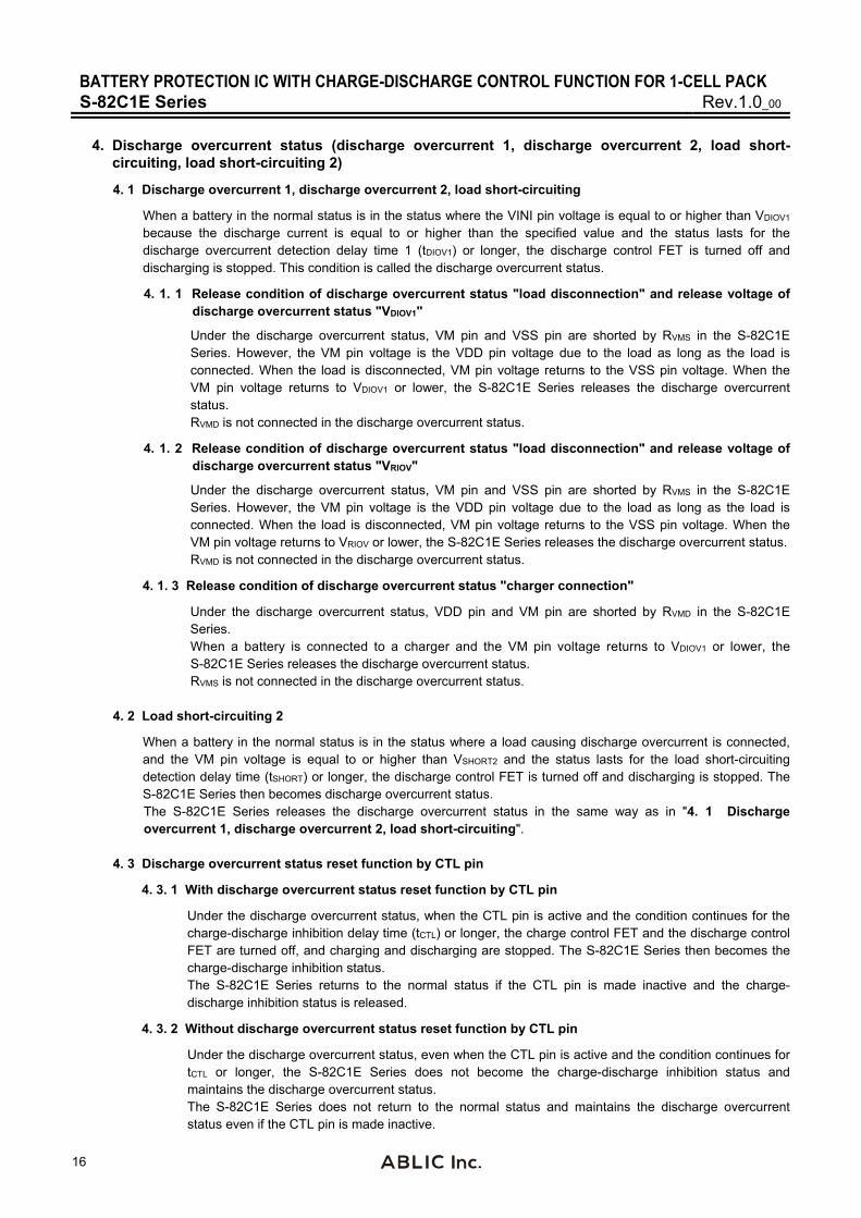
9. Delay circuit
The detection delay times are determined by dividing a clock of approximately 4 kHz by the counter.
Remark tDIOV1, tDIOV2 and tSHORT start when VDIOV1 is detected. When VDIOV2 or VSHORT is detected over tDIOV2 or tSHORT after the detection of VDIOV1, the S-82A1A Series turns the discharge control FET off within tDIOV2 or tSHORT of each detection.
DO pin voltage
VINI pin voltage
VDD
VDD
Time
VDIOV1
VSS
VSS
VSHORT
tSHORT
Time
tD 0 ≤ tD ≤ tSHORT
Figure 8
BATTERY PROTECTION IC WITH CHARGE-DISCHARGE CONTROL FUNCTION FOR 1-CELL PACK Rev.1.0_00 S-82C1E Series
19
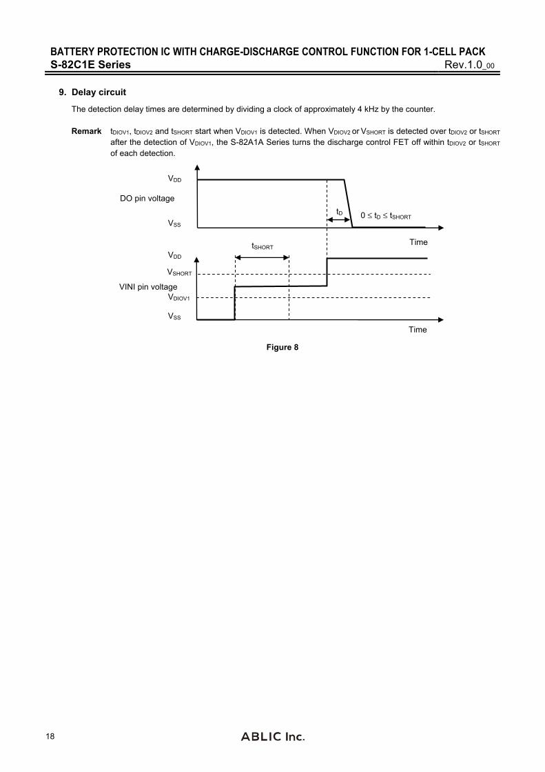
Timing Charts 1. Overcharge detection, overdischarge detection
VCU
VDU (VDL + VHD)VDL
VCL (VCU − VHC)Battery voltage
VSS
CO pin voltage
VDD
DO pin voltage
VSS
Charger connection
Load connection
Status*1(1) (2) (1) (3) (1)
0.35 V typ.VSS
VM pin voltage VDD
VEB−
VDD
VEB−
Overdischarge detection delay time (tDL) Overcharge detection delay time (tCU)
VDIOV1VSS
VINI pin voltage VDD
VCIOV
*1. (1): Normal status (2): Overcharge status (3): Overdischarge status Remark The charger is assumed to charge with a constant current.
Figure 9

BATTERY PROTECTION IC WITH CHARGE-DISCHARGE CONTROL FUNCTION FOR 1-CELL PACK S-82C1E Series Rev.1.0_00
20
2. Discharge overcurrent detection
2. 1 Release condition of discharge overcurrent status "load disconnection"
VRIOV
VDD
VSS
VSHORT
(1) (2) (1) (2)
Load short-circuiting detection delay time (tSHORT)
(1)
VDIVDIOV1
Discharge overcurrent detection delay time 1 (tDIOV1)
VCU
VDU (VDL + VHD)VDL
VCL (VCU − VHC)Battery voltage
VSS
CO pin voltage
VDD
DO pin voltage
VSS
Load connection
Status*1
VM pin voltage
VDD
VSHORT
VDD
VSS
VDIOV2VDIOV1
VINI pin voltage
Discharge overcurrent detection delay time 2 (tDIOV2)
(2) (1)
*1. (1): Normal status (2): Discharge overcurrent status Remark The charger is assumed to charge with a constant current.
Figure 10
BATTERY PROTECTION IC WITH CHARGE-DISCHARGE CONTROL FUNCTION FOR 1-CELL PACK Rev.1.0_00 S-82C1E Series
21
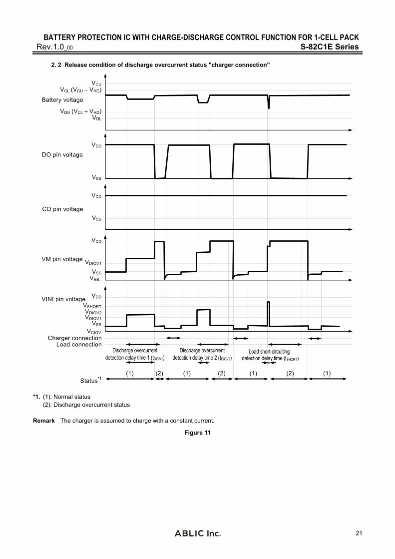
2. 2 Release condition of discharge overcurrent status "charger connection"
VDD
VEB−
(1) (2) (1) (2)
Load short-circuiting detection delay time (tSHORT)
(1)
Discharge overcurrent detection delay time 1 (tDIOV1)
VCU
VDU (VDL + VHD)VDL
VCL (VCU − VHC)Battery voltage
VSS
CO pin voltage
VDD
DO pin voltage
VSS
Load connection
Status*1
VM pin voltage
VDD
VSHORT
VDD
VSS
VDIOV2VDIOV1
VINI pin voltage
Discharge overcurrent detection delay time 2 (tDIOV2)
(2) (1)
VSS
VCIOV
VDIOV1
Charger connection
*1. (1): Normal status (2): Discharge overcurrent status Remark The charger is assumed to charge with a constant current.
Figure 11

BATTERY PROTECTION IC WITH CHARGE-DISCHARGE CONTROL FUNCTION FOR 1-CELL PACK S-82C1E Series Rev.1.0_00
22
3. Charge overcurrent detection
(2)
VDD
VSS
VDD
VSS
VDD
VSS
(3) (1)
VEB−
VEB−
VCU
VDU (VDL + VHD)VDL
VCL (VCU − VHC)
(1) (1) (2)
Battery voltage
DO pin voltage
CO pin voltage
VM pin voltage
Charger connectionLoad connection
Status*1
Charge overcurrent detection delay time (tCIOV)
Overdischarge detection delay time (tDL)
Charge overcurrent detection delay time (tCIOV)
VDD
VSSVCIOV
VINI pin voltage VDIOV1
0.35 V typ.
*1. (1): Normal status (2): Charge overcurrent status (3): Overdischarge status Remark The charger is assumed to charge with a constant current.
Figure 12
BATTERY PROTECTION IC WITH CHARGE-DISCHARGE CONTROL FUNCTION FOR 1-CELL PACK Rev.1.0_00 S-82C1E Series
23
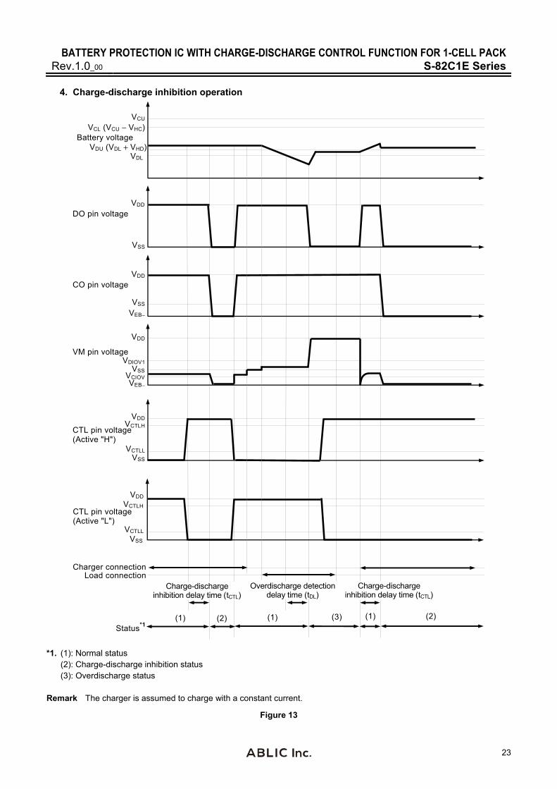
4. Charge-discharge inhibition operation
VDD
DO pin voltage
VSS
VDD
VSS
CO pin voltage
VDD
VSS
VM pin voltage
VCIOV
Status*1(1) (1)
Charger connection
VEB−
VEB−
VCU
VDU (VDL + VHD)VDL
VCL (VCU − VHC) Battery voltage
(2)
Load connection
(3) (2)
VDD
VSS
CTL pin voltage (Active "H")
VDIOV1
(1)
Charge-discharge inhibition delay time (tCTL)
Overdischarge detection delay time (tDL)
VCTLH
VCTLL
VDDVCTLH
VCTLLVSS
CTL pin voltage (Active "L")
Charge-discharge inhibition delay time (tCTL)
*1. (1): Normal status (2): Charge-discharge inhibition status (3): Overdischarge status Remark The charger is assumed to charge with a constant current.
Figure 13
BATTERY PROTECTION IC WITH CHARGE-DISCHARGE CONTROL FUNCTION FOR 1-CELL PACK S-82C1E Series Rev.1.0_00
24
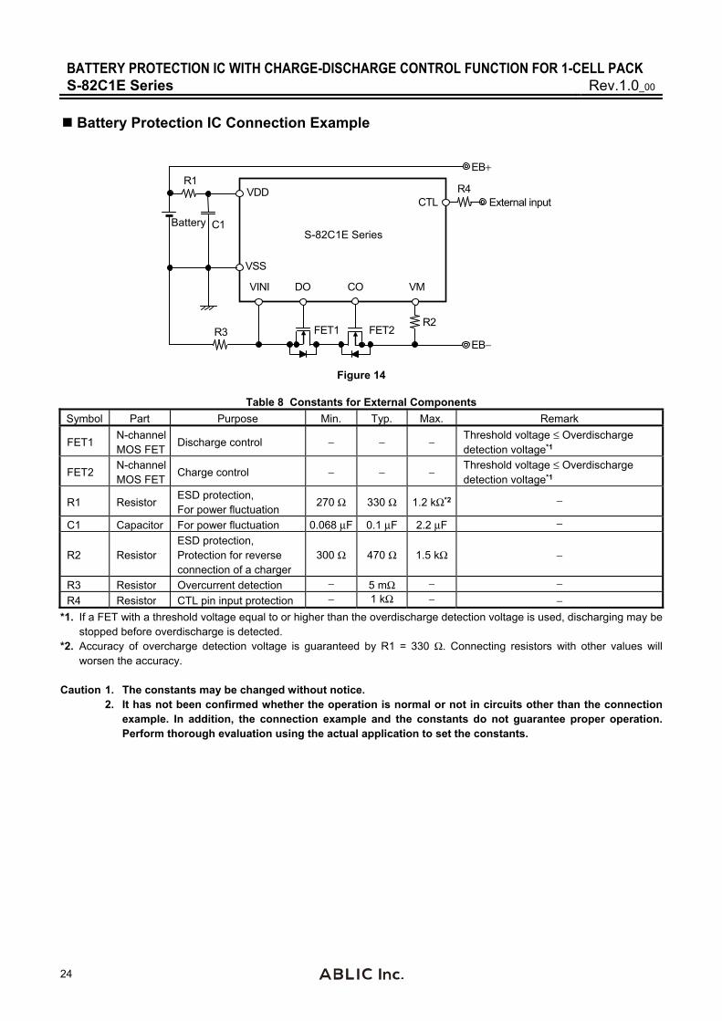
Battery Protection IC Connection Example
DO CO VM
FET1 FET2 R2
VSS
CTL
VINI
R3
R4
Battery
External input
C1
R1 VDD
S-82C1E Series
EB−
EB+
Figure 14
Table 8 Constants for External Components Symbol Part Purpose Min. Typ. Max. Remark
FET1 N-channel MOS FET Discharge control − − − Threshold voltage ≤ Overdischarge
detection voltage*1
FET2 N-channel MOS FET Charge control − − − Threshold voltage ≤ Overdischarge
detection voltage*1
R1 Resistor ESD protection, For power fluctuation 270 Ω 330 Ω 1.2 kΩ*2 −
C1 Capacitor For power fluctuation 0.068 μF 0.1 μF 2.2 μF −
R2 Resistor ESD protection, Protection for reverse connection of a charger
300 Ω 470 Ω 1.5 kΩ −
R3 Resistor Overcurrent detection − 5 mΩ − − R4 Resistor CTL pin input protection − 1 kΩ − −
*1. If a FET with a threshold voltage equal to or higher than the overdischarge detection voltage is used, discharging may be stopped before overdischarge is detected.
*2. Accuracy of overcharge detection voltage is guaranteed by R1 = 330 Ω. Connecting resistors with other values will worsen the accuracy.
Caution 1. The constants may be changed without notice. 2. It has not been confirmed whether the operation is normal or not in circuits other than the connection
example. In addition, the connection example and the constants do not guarantee proper operation. Perform thorough evaluation using the actual application to set the constants.
BATTERY PROTECTION IC WITH CHARGE-DISCHARGE CONTROL FUNCTION FOR 1-CELL PACK Rev.1.0_00 S-82C1E Series
25
Precautions • The application conditions for the input voltage, output voltage, and load current should not exceed the power
dissipation.
• Do not apply an electrostatic discharge to this IC that exceeds the performance ratings of the built-in electrostatic protection circuit.
• ABLIC Inc. claims no responsibility for any and all disputes arising out of or in connection with any infringement by products including this IC of patents owned by a third party.

BATTERY PROTECTION IC WITH CHARGE-DISCHARGE CONTROL FUNCTION FOR 1-CELL PACK S-82C1E Series Rev.1.0_00
26
Marking Specifications
1. DFN-8(1616)A
Top view
1 432
8 567
(1) (2) (3) (4)
(5) (6) (7)
(1): Product code (Blank) (2) to (4): Product code (5) to (7): Lot number

BATTERY PROTECTION IC WITH CHARGE-DISCHARGE CONTROL FUNCTION FOR 1-CELL PACK Rev.1.0_00 S-82C1E Series
27
Power Dissipation
0 25 50 75 100 125 150 1750.0
0.2
0.4
0.6
0.8
1.0
Ambient temperature (Ta) [°C]
Pow
er d
issi
patio
n (P
D) [
W]
Tj = +125°C max.
DFN-8(1616)A
B
A
Board Power Dissipation (PD) A 0.36 W B 0.47 W C − D − E −

(1)
1234
(2)
1234
Board A
Item SpecificationSize [mm] 114.3 x 76.2 x t1.6Material FR-4Number of copper foil layer 2
Copper foil layer [mm]
Land pattern and wiring for testing: t0.070--
74.2 x 74.2 x t0.070
74.2 x 74.2 x t0.070
Thermal via -
Board B
Item SpecificationSize [mm] 114.3 x 76.2 x t1.6
Thermal via -
Material FR-4Number of copper foil layer 4
Copper foil layer [mm]
Land pattern and wiring for testing: t0.07074.2 x 74.2 x t0.03574.2 x 74.2 x t0.035
IC Mount Area
DFN-8(1616)A Test Board
No. DFN8-C-Board-SD-1.0
ABLIC Inc.

���
�����
���
����
������ ��
��
������ �������
���� ������ �������
������������������� ����!������!����"�����#� �"� $�������#�!�$��!��%��������$"�!& ��
'����"���$� ��� ������������ ��$"�!& ��
�������&��������������&� ���������#� �"�!��
��()���*
��+�)���*
��,
�-����'� .������������
��/�)���*
���
�����
���
����
������ ��
��
������'�������
,��)���0��*
���*)��� ��1*)���
��(�)���*(��)���*2���
���
,��)���0��/)���
-��!�!�"� ����
�,
* �
���� ������'�������
�-����'�'�""��"���$�
���
�����
���
����
������ ��
3�4� *5���
���� ������6�������
������6�������
��
0�+)��(
��#�"%�!�!"�7��%�������� ���"�#�$�"�
�-����'�6��#
���,)���
8��2��������
���
�����
���
����
������ ��
��
�-����'
��������������
���� ��������������
'�&��������� ���"� �����!�!������#!�"� �������������� ��������"!��� � � � � � � � � � ����"!�"�������&"�����������"�!�������
.�
��+�
��,�
��(+
������!�6� �����!�����

Disclaimers (Handling Precautions) 1. All the information described herein (product data, specifications, figures, tables, programs, algorithms and
application circuit examples, etc.) is current as of publishing date of this document and is subject to change without notice.
2. The circuit examples and the usages described herein are for reference only, and do not guarantee the success of any specific mass-production design. ABLIC Inc. is not liable for any losses, damages, claims or demands caused by the reasons other than the products described herein (hereinafter "the products") or infringement of third-party intellectual property right and any other right due to the use of the information described herein.
3. ABLIC Inc. is not liable for any losses, damages, claims or demands caused by the incorrect information described herein.
4. Be careful to use the products within their ranges described herein. Pay special attention for use to the absolute maximum ratings, operation voltage range and electrical characteristics, etc. ABLIC Inc. is not liable for any losses, damages, claims or demands caused by failures and / or accidents, etc. due to the use of the products outside their specified ranges.
5. Before using the products, confirm their applications, and the laws and regulations of the region or country where they are used and verify suitability, safety and other factors for the intended use.
6. When exporting the products, comply with the Foreign Exchange and Foreign Trade Act and all other export-related laws, and follow the required procedures.
7. The products are strictly prohibited from using, providing or exporting for the purposes of the development of weapons of mass destruction or military use. ABLIC Inc. is not liable for any losses, damages, claims or demands caused by any provision or export to the person or entity who intends to develop, manufacture, use or store nuclear, biological or chemical weapons or missiles, or use any other military purposes.
8. The products are not designed to be used as part of any device or equipment that may affect the human body, human life, or assets (such as medical equipment, disaster prevention systems, security systems, combustion control systems, infrastructure control systems, vehicle equipment, traffic systems, in-vehicle equipment, aviation equipment, aerospace equipment, and nuclear-related equipment), excluding when specified for in-vehicle use or other uses by ABLIC, Inc. Do not apply the products to the above listed devices and equipments. ABLIC Inc. is not liable for any losses, damages, claims or demands caused by unauthorized or unspecified use of the products.
9. In general, semiconductor products may fail or malfunction with some probability. The user of the products should therefore take responsibility to give thorough consideration to safety design including redundancy, fire spread prevention measures, and malfunction prevention to prevent accidents causing injury or death, fires and social damage, etc. that may ensue from the products' failure or malfunction. The entire system in which the products are used must be sufficiently evaluated and judged whether the products are allowed to apply for the system on customer's own responsibility.
10. The products are not designed to be radiation-proof. The necessary radiation measures should be taken in the product design by the customer depending on the intended use.
11. The products do not affect human health under normal use. However, they contain chemical substances and heavy metals and should therefore not be put in the mouth. The fracture surfaces of wafers and chips may be sharp. Be careful when handling these with the bare hands to prevent injuries, etc.
12. When disposing of the products, comply with the laws and ordinances of the country or region where they are used. 13. The information described herein contains copyright information and know-how of ABLIC Inc. The information
described herein does not convey any license under any intellectual property rights or any other rights belonging to ABLIC Inc. or a third party. Reproduction or copying of the information from this document or any part of this document described herein for the purpose of disclosing it to a third-party is strictly prohibited without the express permission of ABLIC Inc.
14. For more details on the information described herein or any other questions, please contact ABLIC Inc.'s sales representative.
15. This Disclaimers have been delivered in a text using the Japanese language, which text, despite any translations into the English language and the Chinese language, shall be controlling.
2.4-2019.07
www.ablic.com