Embed Size (px)
Citation preview

RTL-to-Gates Synthesis using Synopsys Design Compiler
CS250 Tutorial 5 (Version 091210b)September 12, 2010
Yunsup Lee
In this tutorial you will gain experience using Synopsys Design Compiler (DC) to perform hardwaresynthesis. A synthesis tool takes an RTL hardware description and a standard cell library as inputand produces a gate-level netlist as output. The resulting gate-level netlist is a completely structuraldescription with standard cells only at the leaves of the design. Internally, a synthesis tool performsmany steps including high-level RTL optimizations, RTL to unoptimized boolean logic, technologyindependent optimizations, and finally technology mapping to the available standard cells. GoodRTL designers will familiarize themselves with the target standard cell library so that they candevelop an intuition on how their RTL will be synthesized into gates. In this tutorial you will useSynopsys Design Compiler to elaborate RTL, set optimization constraints, synthesize to gates, andprepare various area and timing reports. You will also learn how to read the various DC text reportsand how to use the graphical Synopsys Design Vision tool to visualize the synthesized design.
Synopsys provides a library called Design Ware which includes highly optimized RTL for arithmeticbuilding blocks. DC can automatically determine when to use Design Ware components and it canthen efficiently synthesize these components into gate-level implementations. In this tutorial youwill learn more about what Design Ware components are available and how to best encourage DCto use them.
The following documentation is located in the course locker (~cs250/manuals) and provides ad-ditional information about Design Compiler, Design Vision, the Design Ware libraries, and theSynopsys 90nm Standard Cell Library.
• dc-user-guide.pdf - Design Compiler User Guide
• dc-quick-reference.pdf - Design Compiler Quick Reference
• dc-user-guide-cli.pdf - Design Compiler Command-Line Interface Guide
• dc-user-guide-lp.pdf - Synopsys Low-Power Flow User Guide
• dc-user-guide-verilog.pdf - HDL Compiler for Verilog User Guide
• dc-user-guide-sysverilog.pdf - HDL Compiler for SystemVerilog User Guide
• dc-user-guide-tcl.pdf - Using Tcl With Synopsys Tools
• dc-user-guide-tco.pdf - Synopsys Timing Constraints and Optimization User Guide
• dc-reference-manual-opt.pdf - Design Compiler Optimization Reference Manual
• dc-reference-manual-rt.pdf - Design Compiler Register Retiming Reference Manual
• dc-application-note-sdc.pdf - Synopsys Design Constraints Format Application Note
• dc dv-user-guide.pdf - Design Vision User Guide
• dc dv-tutorial.pdf - Design Compiler Tutorial Using Design Vision
• designware-intro.pdf - DesignWare Building Block IP Documentation Overview
• designware-user-guide.pdf - DesignWare Building Block IP
• designware-quick-reference.pdf - DesignWare Building Block IP Quick Reference
• designware-datasheets - Directory containing datasheets on each DW component
• synopsys-90nm-databook-stdcells.pdf - Digital Standard Cell Library Databook

CS250 Tutorial 5 (Version 091210b), Fall 2010 2
Getting started
You can follow along through the tutorial yourself by typing in the commands marked with a ’%’symbol at the shell prompt. To cut and paste commands from this tutorial into your bash shell(and make sure bash ignores the ’%’ character) just use an alias to ”undefine” the ’%’ characterlike this:
% alias %=""
All of the CS250 tutorials should be ran on an EECS Instructional machine. Please see the coursewebsite for more information on the computing resources available for CS250 students. Once youhave logged into an EECS Instructional you will need to setup the CS250 toolflow with the followingcommands.
% source ~cs250/tools/cs250.bashrc
For this tutorial you will be using an unpipelined RISC-V v1 processor as your example RTL design.Figure 1 shows the system diagram which is implemented by the example code.
+4
Instruction Mem Reg
File
SignExtend
Decoder
>>1
Cmp
Data Mem
ir[24:20]
branchpc+4
pc_s
el
rd0rd1 Add
ControlSignals
eq?
wb_
sel
RegFile
ir[24
:20]
rf_w
en
val
rw
PC
tohosttestrig_tohost
tohost_en
val
op0
op1
addrwdata
rdata
ir[19:15]
ir[11:0]
Figure 1: Block diagram for Unpipelined RISC-V v1 Processor
You should create a working directory and copy files from the course locker using the followingcommands.
% mkdir tut5
% cd tut5
% TUTROOT=$PWD
% cp -R ~cs250/examples/v-riscv-v1-1stage/* $TUTROOT

CS250 Tutorial 5 (Version 091210b), Fall 2010 3
Before starting, take a look at the subdirectories in the project directory. When pushing designsthrough the physical toolflow you will often refer to the core. The core module contains everythingwhich will be on-chip, while blocks outside the core are assume to be off-chip. For this tutorialyou are assuming that the processor and a combinational memory are located within the core. Acombinational memory means that the read address is specified at the beginning of the cycle, andthe read data returns during the same cycle. Building large combinational memories is relativelyinefficient. It is much more common to use synchronous memories. A synchronous memory meansthat the read address is specified at the end of a cycle, and the read data returns during thenext cycle. From Figure 1 it should be clear that the unpipelined RISC-V v1 processor requirescombinational memories (or else it would turn into a four stage pipeline). For this tutorial youwill not be using a real combinational memory, but instead this combinational memorywill be simulated inside the test harness. Therefore, riscvProc will be the top module thatyou will be pushing through the toolflow in this tutorial. In later tutorials, you will start usingsynchronous on-chip SRAMs, and this case riscvCore will be the top module you will be pushingthrough the toolflow. Figure 2 shows the relationship among these hierarchies in more detail. Thegrey part depicts the test harness.
riscvTestHarness
riscvCore
riscvProc
InstructionMemory
DataMemory
comb0_delay
imem_access_delay
dmem_access_delay
comb1_delay
clock period
Figure 2: Setup for the unpipelined RISC-V v1 Core
In order to synthesize the processor correctly with the two combinational memory, you need tospecify the input and output delays carefully. The input and output delays are marked on one clockperiod in figure 2. The output delay of the instruction request signals from the processor (inputsignals to the instruction memory) should be specified as clock period - comb0 delay. The input delay

CS250 Tutorial 5 (Version 091210b), Fall 2010 4
of the instruction response signals to the processor (output signals from the instruction memory)can be described as comb0 delay + imem access delay. The output delay of the data request signalsfrom the processor (input signals to the data memory) should be specified as dmem access delay+ comb1 delay. The input delay of the data response signals to the processor (output signals fromthe data memory) can be described as clock period - comb1 delay. These constants are specified inbuild/Makefrag.
The build directory will also contain all generated content including simulators, synthesized gate-level Verilog, and final layout. In this course you will always try to keep generated content separatefrom your source RTL. This keeps your project directories well organized, and helps prevent youfrom unintentionally modifying your source RTL. There are subdirectories in the build directoryfor each major step in the CS250 toolflow. These subdirectories contain scripts and configurationfiles for running the tools required for that step in the toolflow. For this tutorial you will workexclusively in the dc-syn.
Synthesizing the Processor
You will begin by running several DC commands manually before learning how you can automatethe tool with scripts. DC can generate a large number of output files, so you will be running DCwithin a build directory beneath dc-syn. Use the following commands to create a build directoryfor DC and to start the DC shell. To cut and past commands from this lab into your DesignCompiler shell and make sure Design Compiler ignores the dc shell-topo> string, we will use analias to ”undefine” the dc shell-topo> string.
% cd $TUTROOT/build/dc-syn
% mkdir manual
% cd manual
% dc_shell-xg-t -64bit -topographical_mode
...
Initializing...
dc_shell-topo> alias "dc_shell-topo>" ""
You should be left at the DC shell prompt from which you can can execute various commands toload in your design, specify constraints, synthesize your design, print reports, etc. You can getmore information about a specific command by entering man <command> at the dc shell prompt.You will now execute some commands to setup your environment.
dc_shell-topo> set ucb_vlsi_home [getenv UCB_VLSI_HOME]
dc_shell-topo> set stdcells_home \
$ucb_vlsi_home/stdcells/synopsys-90nm/default
dc_shell-topo> set_app_var search_path \
"$stdcells_home/db $ucb_vlsi_home/install/vclib ../../../src"
dc_shell-topo> set_app_var target_library "cells.db"
dc_shell-topo> set_app_var synthetic_library "dw_foundation.sldb"
dc_shell-topo> set_app_var link_library "* $target_library $synthetic_library"
dc_shell-topo> set_app_var alib_library_analysis_path "$stdcells_home/alib"
dc_shell-topo> set_app_var mw_logic1_net "VDD"
dc_shell-topo> set_app_var mw_logic0_net "VSS"

CS250 Tutorial 5 (Version 091210b), Fall 2010 5
dc_shell-topo> create_mw_lib -technology $stdcells_home/techfile/techfile.tf \
-mw_reference_library $stdcells_home/mw/cells.mw "riscvProc_LIB"
dc_shell-topo> open_mw_lib "riscvProc_LIB"
dc_shell-topo> check_library
dc_shell-topo> set_tlu_plus_file \
-max_tluplus $stdcells_home/tluplus/max.tluplus \
-min_tluplus $stdcells_home/tluplus/min.tluplus \
-tech2itf_map $stdcells_home/techfile/tech2itf.map
dc_shell-topo> check_tlu_plus_files
dc_shell-topo> define_design_lib WORK -path "./work"
These commands point to your Verilog source directory, create a Synopsys work directory, andpoint to the standard libraries you will be using for this class. The DB file contains timing/areainformation for each standard cell, and the Milkyway library contains wireload models. DC willuse this information to try and optimize the synthesis process. You can now load your Verilogdesign into Design Compiler with the analyze, elaborate, and link commands. Executing thesecommands will result in a great deal of log output as the tool elaborates some Verilog constructsand starts to infer some high-level components. Try executing the commands as follows.
dc_shell-topo> analyze -format verilog \
"defCommon.vh riscvInst.vh riscvConst.vh \
riscvProcCtrl.v riscvProcDpathRegfile.v riscvProcDpath.v \
riscvProc.v"
dc_shell-topo> elaborate "riscvProc"
dc_shell-topo> link
Take a closer look at the output during elaboration. DC will report all state inferences. This is agood way to verify that latches and flip-flops are not being accidentally inferred. You should beable to check that the only inferred state elements are the PC, the tohost register, a one-bit resetregister, and the register file. DC will also note information about inferred muxes. Figure 3 showsa fragment from the elaboration output text. From this output you can see that DC is inferring32-bit flip-flops for the register file and two 32 input 32-bit muxes for the register file read ports. Seethe HDL Compiler for Verilog User Guide (dc-user-guide-verilog.pdf) for more informationon the output from the elaborate command and more generally how DC infers combinational andsequential hardware elements.
After reading your design into DC you can use the check design command to check that the designis consistent. A consistent design is one which does not contain any errors such as unconnectedports, constant-valued ports, cells with no input or output pins, mismatches between a cell and itsreference, multiple driver nets, connection class violations, or recursive hierarchy definitions. Youwill not be able to synthesize your design until you eliminate any errors. Many of these warningare obviously not an issue, but it is still useful to skim through this output.
dc_shell-topo> check_design
Before you can synthesize your design, you must specify some constraints; most importantly youmust tell the tool your target clock period. The following commands tell the tool that the pinnamed clk is the clock and that your desired clock period is 2.5 nanoseconds. You need to set theclock period constraint carefully. If the period is unrealistically small, then the tools will spend

CS250 Tutorial 5 (Version 091210b), Fall 2010 6
in routine riscvProcDpathRegfile line 26 in file
’../../../src/riscvProcDpathRegfile.v’.
===============================================================================
| Register Name | Type | Width | Bus | MB | AR | AS | SR | SS | ST |
===============================================================================
| registers_reg | Flip-flop | 32 | Y | N | N | N | N | N | N |
...
| registers_reg | Flip-flop | 32 | Y | N | N | N | N | N | N |
===============================================================================
Statistics for MUX_OPs
===================================================================
| block name/line | Inputs | Outputs | # sel inputs | MB |
===================================================================
| riscvProcDpathRegfile/22 | 32 | 32 | 5 | N |
| riscvProcDpathRegfile/23 | 32 | 32 | 5 | N |
===================================================================
Figure 3: Output from the Design Compiler elaborate command
forever trying to meet timing and ultimately fail. If the period is too large, then the tools willhave no trouble but you will get a very conservative implementation. You also need to specify theinput and output delays discussed in figure 2. For more information about constraints consult theSynopsys Timing Constraints and Optimization User Guide (dc-user-guide-tco.pdf).
dc_shell-topo> create_clock clk -name ideal_clock1 -period 2.5
dc_shell-topo> set_output_delay -clock ideal_clock1 2.3 imemreq_bits_addr
dc_shell-topo> set_output_delay -clock ideal_clock1 2.3 imemreq_val
dc_shell-topo> set_input_delay -clock ideal_clock1 0.6 imemresp_bits_data
dc_shell-topo> set_output_delay -clock ideal_clock1 0.65 dmemreq_bits_rw
dc_shell-topo> set_output_delay -clock ideal_clock1 0.65 dmemreq_bits_addr
dc_shell-topo> set_output_delay -clock ideal_clock1 0.65 dmemreq_bits_data
dc_shell-topo> set_output_delay -clock ideal_clock1 0.65 dmemreq_val
dc_shell-topo> set_input_delay -clock ideal_clock1 2.25 dmemresp_bits_data
Now you are ready to use the compile ultra command to actually synthesize your design intoa gate-level netlist. -gate clock enables clock gating. -no autoungroup is specified in order topreserve the hierarchy during synthesis or disable inter-module optimizations. With no optionsgiven, compile ultra command optimizes across module boundaries. For more information on thecompile ultra command consult the Design Compiler User Guide (dc-user-guide.pdf) or useman compile ultra at the DC shell prompt. Run the following command and take a look at theoutput.
DC will attempt to synthesize your design while still meeting the constraints. DC considers twotypes of constraints: user specified constraints and design rule constraints. User specified constraintscan be used to constrain the clock period (as you saw with the create clock command) but theycan also be used to constrain the arrival of certain input signals, the drive strength of the inputsignals, and the capacitive load on the output signals. Design rule constraints are fixed constraintswhich are specified by the standard cell library. For example, there are restrictions on the loadsspecific gates can drive and on the transition times of certain pins. For more information consultSynopsys Design Constraints Format Application Note (dc-application-note-sdc.pdf).

CS250 Tutorial 5 (Version 091210b), Fall 2010 7
dc_shell-topo> compile_ultra -gate_clock -no_autoungroup
The compile command will report how the design is being optimized. You should see DC performingtechnology mapping, delay optimization, and area reduction. Figure 4 shows a fragment from thecompile output. Each line is an optimization pass. The area column is in units specific to thestandard cell library which is um2, but for now you should just use the area numbers as a relativemetric. The worst negative slack column shows how much room there is between the critical pathin your design and the clock constraint. Larger negative slack values are worse since this meansthat your design is missing the desired clock frequency by a greater amount. Total negative slackis the sum of all negative slack across all endpoints in the design - if this is a large negative numberit indicates that not only is the design not making timing, but it is possible that many paths aretoo slow. If the total negative slack is a small negative number, then this indicates that only afew paths are too slow. The design rule cost is a indication of how many cells violate one of thestandard cell library design rules constraints. Figure 4 shows that on the first iteration, the toolmakes timing but at a high area cost, so on the second iteration it optimizes area but this causesthe design to no longer meet timing. The tool continues to optimize until it meets the constraints.
...
ELAPSED WORST NEG TOTAL NEG DESIGN LEAKAGE
TIME AREA SLACK SLACK RULE COST ENDPOINT POWER
--------- --------- --------- --------- --------- ------------- ---------
0:00:25 56092.3 0.68 193.7 0.0 308556192.0000
Beginning Delay Optimization
----------------------------
0:00:28 51442.8 0.28 5.4 0.0 274241280.0000
0:00:28 51589.3 0.23 4.5 0.0 275486656.0000
0:00:28 51589.3 0.23 4.5 0.0 275486656.0000
0:00:33 52530.3 0.12 2.1 0.0 281122144.0000
0:00:33 52530.3 0.12 2.1 0.0 281122144.0000
0:00:35 54100.7 0.00 0.0 0.0 295563680.0000
0:00:35 54100.7 0.00 0.0 0.0 295563680.0000
0:00:35 54100.7 0.00 0.0 0.0 295563680.0000
...
Figure 4: Output from the Design Compiler compile ultra command
You can now use various commands to examine timing paths, display reports, and further optimizeyour design. Entering in these commands by hand can be tedious and error prone, plus doingso makes it difficult to reproduce a result. Thus you will mostly use TCL scripts to control thetool. Even so, using the shell directly is useful for finding out more information about a specificcommand or playing with various options.
Before continuing, exit the DC shell and delete your build directory with the following commands.
dc_shell-topo> exit
% cd $TUTROOT/build/dc-syn
% rm -rf manual
CS250 Tutorial 5 (Version 091210b), Fall 2010 8
Automating Synthesis with TCL Scripts and Makefiles
In this section you will examine how to use various TCL scripts and makefiles to automate thesynthesis process. There are a couple files you should take a close look in the build directory.
• Makefrag - Makefile fragment file which contains clock period
• dc-syn/Makefile - Makefile for driving synthesis with the TCL scripts
• dc-syn/rm dc scripts/dc.tcl - Primary TCL script which contains the DC commands
• dc-syn/rm dc scripts/find regs.tcl - TCL script which finds all reigsters
• dc-syn/rm setup/common setup.tcl - TCL fragment for various common variables
• dc-syn/rm setup/dc setup.tcl - TCL fragment for various library variables
• dc-syn/rm setup/dc setup filenames.tcl - TCL fragment for various filename variables
• dc-syn/constraints.tcl - User specified constraints
First take a look at the Makefrag file. This file contains the desired clock period. Notice that ituses a shorter clock period (90% of the desired clock period) for synthesis in order to leave someslack for place and route. Now open up the dc setup.tcl script. You will see that it sets upseveral library variables, creates the search path, and instructs DC to use a work directory. Thefirst line of the dc setup.tcl script loads the make generated vars.tcl script. This script isgenerated by the makefile and it contains variables which are defined by the makefile and used bythe TCL scripts. You will take a closer look at it in a moment. Now examine the dc.tcl script.You will see many familiar commands which we executed by hand in the previous section. Youwill also see some new commands. Take a closer look at the bottom of this TCL script where wewrite out several text reports. Remember that you can get more information on any command byusing man <command> at the DC shell prompt. The constraints.tcl file contains various userspecified constraints. You specify that DC should assume that minimum sized inverters are drivingthe inputs to the design and that the outputs must drive 4 fF of capacitance.
Now that you are more familiar with the various TCL scripts, you will see how to use the makefile todrive synthesis. Look inside the makefile and identify where the Verilog sources and the C sourcesare defined. Notice that the test harness is not included. You should only list those Verilog fileswhich are part of the processor; do not included non-synthesizable test harnesses modules. Alsonotice that we must identify the toplevel Verilog module in the design, toplevel instance, and finallythe test harness module. The build rules in the makefile will create new build directories, copy theTCL scripts into these build directories, and then run DC. Use the following make target to createa new build directory.
% cd $TUTROOT/build/dc-syn
% make new-build-dir
You should now see a new build directory named build-<date> where <date> represents the timeand date. The current-dc symlink always points to the most recent build directory. If you look in-side the build directory, you will see the common setup.tcl, dc setup.tcl, dc setup filenames.tcl,dc.tcl, find regs.tcl and constraints.tcl scripts but you will also see an additional make generated vars.tcl
script. Various variables inside make generated vars.tcl are used to specify the search path,which Verilog files to read in, which modules should be marked don’t touch, the toplevel Verilogname, etc. After using make new-build-dir you can cd into the current-dc directory, start theDC shell, and run DC commands by hand. For example, the following sequence will perform thesame steps as in the previous section.

CS250 Tutorial 5 (Version 091210b), Fall 2010 9
% cd $TUTROOT/build/dc-syn
% cd current-dc
% dc_shell-xg-t -64bit -topographical_mode
dc_shell-topo> alias "dc_shell-topo>" ""
dc_shell-topo> source dc_setup.tcl
dc_shell-topo> define_design_lib WORK -path ./work
dc_shell-topo> analyze -format verilog ${RTL_SOURCE_FILES}
dc_shell-topo> elaborate ${DESIGN_NAME}
dc_shell-topo> link
dc_shell-topo> source constraints.tcl
dc_shell-topo> compile_ultra -gate_clock -no_autoungroup
dc_shell-topo> exit
The new-build-dir make target is useful when you want to conveniently run through some DCcommands by hand to try them out. To completely automate your synthesis you can use the dc
make target (which is also the default make target). For example, the following commands willautomatically synthesize the design and save several text reports to the build directory.
% cd $TUTROOT/build/dc-syn
% make dc
You should see DC compiler start and then execute the commands located in the dc.tcl script.Once synthesis is finished try running make dc again. The makefile will detect that nothing haschanged (i.e. the Verilog source files and DC scripts are the same) and so it does nothing. EditMakefrag and change the clock period constraint to 10 ns. Now use make dc to resynthesize thedesign. Since you changed the clock period, make will correctly run DC again. Take a look at thecurrent contents of dc-syn.
% cd $TUTROOT/build/dc-syn
% ls -l
total 32
-rw-r--r-- 1 yunsup grad 5003 Sep 12 10:52 Makefile
drwxr-xr-x 7 yunsup grad 4096 Sep 12 11:12 build-dc-2010-09-12_11-11
drwxr-xr-x 7 yunsup grad 4096 Sep 12 11:14 build-dc-2010-09-12_11-13
-rw-r--r-- 1 yunsup grad 1712 Sep 12 10:52 constraints.tcl
lrwxrwxrwx 1 yunsup grad 25 Sep 12 11:13 current-dc -> build-dc-2010-09-12_11-13
drwxr-xr-x 2 yunsup grad 4096 Sep 12 10:52 rm_dc_scripts
drwxr-xr-x 2 yunsup grad 4096 Sep 12 10:52 rm_notes
drwxr-xr-x 2 yunsup grad 4096 Sep 12 10:52 rm_setup
Notice that the makefile does not overwrite build directories. It always creates new build directories.This makes it easy to change your synthesis scripts or source Verilog, resynthesize your design, andcompare your results to previous designs. You can use symlinks to keep track of what various builddirectories correspond to. For example, the following commands label the build directory whichcorresponds to a 2.5 ns clock period constraint and the build directory which corresponds to a 10 nsclock period constraint.
% cd $TUTROOT/build/dc-syn
% ln -s build-dc-2010-09-12_11-11 build-2.5ns
% ln -s build-dc-2010-09-12_11-13 build-10ns

CS250 Tutorial 5 (Version 091210b), Fall 2010 10
Every so often you should delete old build directories to save space. The make clean command willdelete all build directories so use it carefully. Sometimes you want to really force the makefile toresynthesize the design but for some reason it may not work properly. To force a resynthesis withoutdoing a make clean simply remove the current symlink. For example, the following commandswill force a resynthesis without actually changing any of the source TCL scripts or Verilog.
% cd $TUTROOT/build/dc-syn
% rm -f current-dc
% make dc
Interpreting the Synthesized Gate-Level Netlist and Text Reports
In this section you will examine some of the output which our dc.tcl script generates. You willinitially focus on the contents of the build-2.5ns build directory. The primary output from the syn-thesis scripts is the synthesized gate-level netlist which is contained in results/riscvProc.mapped.v.Take a look at the gate-level netlist for the 2.5 ns clock constraint. Notice that the RTL modulehierarchy is preserved in the gate-level netlist since you did not flatten any part of your design.Find the four two-input multiplexers in the gate-level netlist by searching for riscvProcDpathMux.Although the same two-input mux was instantiated four times in the design (the PC mux, theAdder operand muxes, and the writeback mux), DC has optimized each multiplexer differently.Figure 5 shows the gate-level netlist for the synthesized multiplexers.
From the gate-level netlist you can determine that the tool synthesized different types of muxes. ThePC mux, operand 1 mux, and the write back mux used MUX21X1 standard cells with some buffers.Usethe databook for the Synopsys 90nm Standard Cell Library (synopsys-90nm-databook-stdcells.pdf)to determine the function of the MUX21X1 standard cell. You should discover that this is a 2 input1-bit mux cell. Notice that the pc mux used 32 MUX21X1 cells. In constrast, op 0 mux used a lot ofrandom standard cells. Looking back into figure 1, you can notice that one of the input operandcomes from register file. The tool has figured out that op 0 mux is on the critical path, and selecteda different architecture (a combinational reduction tree) to implement a mux. All input operandsof op 1 mux comes directly from the instruction, and therefore it changed less MUX21X1 standardcells into a reduction tree.
In addition to the actual synthesized gate-level netlist, the dc.tcl also generates several reports.Reports usually have the rpt filename suffix. The following is a list of the synthesis reports.
• reports/*.mapped.area.rpt - Area information for each module instance
• reports/*.mapped.clock gating.rpt - Clock gating information
• reports/*.mapped.power.rpt - Power information for each module instance
• reports/*.mapped.qor.rpt - QoR (Quality of Result) information and statistics
• reports/*.mapped.reference.rpt - Information on references
• reports/*.mapped.resources.rpt - Information on Design Ware components
• reports/*.mapped.timing.rpt - Contains critical timing paths
• log/dc.log - Log file of all output during DC run

CS250 Tutorial 5 (Version 091210b), Fall 2010 11
module riscvProcDpathMux_0 ( sel, in0, in1, out ); // pc mux
...
MUX21X1 U10 ( .IN1(in0[15]), .IN2(in1[15]), .S(n3), .Q(out[15]) );
MUX21X1 U11 ( .IN1(in0[16]), .IN2(in1[16]), .S(n3), .Q(out[16]) );
MUX21X1 U12 ( .IN1(in0[17]), .IN2(in1[17]), .S(n3), .Q(out[17]) );
MUX21X1 U13 ( .IN1(in0[18]), .IN2(in1[18]), .S(n3), .Q(out[18]) );
MUX21X1 U14 ( .IN1(in0[19]), .IN2(in1[19]), .S(n3), .Q(out[19]) );
MUX21X1 U15 ( .IN1(in0[20]), .IN2(in1[20]), .S(n3), .Q(out[20]) );
...
endmodule
module riscvProcDpathMux_3 ( sel, in0, in1, out ); // op0 mux
...
NAND2X2 U2 ( .IN1(n7), .IN2(n6), .QN(out[2]) );
NAND2X2 U19 ( .IN1(in1[9]), .IN2(sel), .QN(n10) );
NAND2X2 U24 ( .IN1(n13), .IN2(n12), .QN(out[11]) );
NAND2X2 U28 ( .IN1(n16), .IN2(n15), .QN(out[29]) );
NAND2X2 U32 ( .IN1(n19), .IN2(n18), .QN(out[28]) );
NAND2X2 U36 ( .IN1(n22), .IN2(n21), .QN(out[7]) );
NAND2X2 U40 ( .IN1(n25), .IN2(n24), .QN(out[25]) );
NAND2X2 U52 ( .IN1(n34), .IN2(n33), .QN(out[14]) );
NAND2X2 U58 ( .IN1(n57), .IN2(n56), .QN(out[16]) );
...
endmodule
module riscvProcDpathMux_2 ( sel, in0, in1, out ); // op1 mux
...
MUX21X1 U14 ( .IN1(in0[1]), .IN2(in0[0]), .S(sel), .Q(out[1]) );
MUX21X1 U15 ( .IN1(in0[4]), .IN2(in0[3]), .S(sel), .Q(out[4]) );
MUX21X1 U16 ( .IN1(in0[5]), .IN2(in0[4]), .S(sel), .Q(out[5]) );
MUX21X1 U17 ( .IN1(in0[6]), .IN2(in0[5]), .S(sel), .Q(out[6]) );
MUX21X1 U18 ( .IN1(in0[7]), .IN2(in0[6]), .S(sel), .Q(out[7]) );
MUX21X1 U19 ( .IN1(in1[10]), .IN2(in0[8]), .S(sel), .Q(out[9]) );
MUX21X1 U20 ( .IN1(in0[10]), .IN2(in1[10]), .S(sel), .Q(out[10]) );
MUX21X1 U21 ( .IN1(in0[11]), .IN2(in0[10]), .S(sel), .Q(out[11]) );
...
endmodule
module riscvProcDpathMux_1 ( sel, in0, in1, out ); // wb mux
...
MUX21X2 U37 ( .IN1(in0[10]), .IN2(in1[10]), .S(n35), .Q(out[10]) );
MUX21X2 U51 ( .IN1(in0[24]), .IN2(in1[24]), .S(n34), .Q(out[24]) );
MUX21X2 U50 ( .IN1(in0[23]), .IN2(in1[23]), .S(n34), .Q(out[23]) );
MUX21X2 U58 ( .IN1(in0[31]), .IN2(in1[31]), .S(n33), .Q(out[31]) );
MUX21X2 U55 ( .IN1(in0[28]), .IN2(in1[28]), .S(n33), .Q(out[28]) );
MUX21X2 U54 ( .IN1(in0[27]), .IN2(in1[27]), .S(n34), .Q(out[27]) );
MUX21X2 U52 ( .IN1(in0[25]), .IN2(in1[25]), .S(n34), .Q(out[25]) );
...
endmodule
Figure 5: Gate-Level Netlist for Two Synthesized 32 Input 32-bit Muxes

CS250 Tutorial 5 (Version 091210b), Fall 2010 12
In this section you will discuss the area.rpt, timing.rpt, and the reference.rpt reports. Thenext section will discuss the resources.rpt report. The area.rpt report contains area infor-mation for each module in the design. Figure 6 shows a fragment from area.rpt for the RISC-V v1 unpipelined processor. You can use the reference.rpt report (Figure 7 to gain insightinto how various modules are being implemented. For example, you can use the reference re-port in a similar fashion as the results/riscvProc.mapped.v gate-level netlist to see that theriscvProcDpathMux 2 (op 1 mux) module includes only 8 mux cell.
Global cell area Local cell area
------------------- ------------------------------
Hierarchical cell Absolute Percent Combi- Noncombi- Black
Total Total national national boxes
-------------------------------- ---------- ------- ---------- ---------- ------
riscvProc 53125.7656 100.0 32.2560 49.7664 0.0000
ctrl 259.8913 0.5 259.8913 0.0000 0.0000
dpath 52783.8516 99.4 5336.9897 1045.0942 0.0000
dpath/add_in0_mux 970.4451 1.8 970.4451 0.0000 0.0000
dpath/add_in1_mux 145.6128 0.3 145.6128 0.0000 0.0000
dpath/clk_gate_tohost_reg_reg 37.7856 0.1 12.9024 24.8832 0.0000
dpath/pc_mux 364.9537 0.7 364.9537 0.0000 0.0000
dpath/rfile 44453.7031 83.7 18652.0801 24683.9023 0.0000
dpath/rfile/clk_gate_registers_reg_10_ 35.9424 0.1 13.8240 22.1184 0.0000
...
dpath/rfile/clk_gate_registers_reg_9_ 35.9424 0.1 13.8240 22.1184 0.0000
dpath/wdata_mux 429.4657 0.8 429.4657 0.0000 0.0000
-------------------------------- ---------- ------- ---------- ---------- ------
Total 26633.1465 26493.0254 0.0000
Figure 6: Fragment from riscvProc.mapped.area.rpt
****************************************
Design: riscvProcDpathMux_2
****************************************
Reference Library Unit Area Count Total Area Attributes
-----------------------------------------------------------------------------
AND2X1 saed90nm_typ 7.372800 1 7.372800
INVX0 saed90nm_typ 5.529600 2 11.059200
INVX2 saed90nm_typ 6.451200 1 6.451200
MUX21X1 saed90nm_typ 11.059200 8 88.473602
NAND2X0 saed90nm_typ 5.529600 7 38.707201
NAND2X1 saed90nm_typ 5.529600 2 11.059200
-----------------------------------------------------------------------------
Total 6 references 163.123204
Figure 7: Fragment from riscvProc.mapped.reference.rpt
You can also use the area report to measure the relative area of the various modules. The reportclearly shows that the majority of the processor area is in the datapath. More specifically you cansee that register file consumes 84% of the total processor area. The reference report reveals thatthe register file is being implemented with approximately 1000 enable flip-flops and input muxes(for the read ports). This is a very inefficient way to implement a register file, but it is the best the

CS250 Tutorial 5 (Version 091210b), Fall 2010 13
synthesizer can do. Real ASIC designers rarely synthesize memories and instead turn to memorygenerators. A memory generator is a tool which takes an abstract description of the memory blockas input and produces a memory in formats suitable for various tools. Memory generators usecustom cells and procedural place+route to achieve an implementation which can be an order ofmagnitude better in terms of performance and area than synthesized memories.
Figure 8,9,10 illustrates a fragment of the timing report found in timing.rpt. The report lists thecritical path of the design. The critical path is the slowest logic path between any two registers andis therefore the limiting factor preventing you from decreasing the clock period constraint (and thusincreasing performance). The report is generated from a purely static worst-case timing analysis(i.e. independent of the actual signals which are active when the processor is running). The firstcolumn lists various nodes in the design. Note that several nodes internal to higher level moduleshave been cut out to save space. The last column lists the cumulative delay to that node, whilethe middle column shows the incremental delay.
Since we specified our delays to incorporate combinational memory (described in figure 2, we shouldhave three types of critical paths. Starting from the PC register to the instruction memory requestports (shown in figure 8), instruction memory response ports to data memory request ports (shownin figure 9), and finally data memory response ports to register file write ports (shown in figure 10).
You can see that the critical path in figure 8 starts at the second bit of the PC register; ends atthe instruction memory request port before 0.2 ns. The critical path in figure 9 starts from theinstruction memory response port at 0.6 ns; goes through register file decode logic; goes through theop 0 mux; goes through the adder; and finally ends at the data memory request port at 1.6 ns. Thelast critical path in figure 10 starts from the data memory response port at 2.0 ns; goes through thewrite back mux; ends at the register write port at 2.25 ns. The reason why it’s 2.25 ns not 2.5 ns isbecause we set up a shorter clock period for synthesis to leave some slack for place and route.
Point Fanout Cap Trans Incr Path
-----------------------------------------------------------------------------------------
clock ideal_clock1 (rise edge) 0.0000 0.0000
clock network delay (ideal) 0.0000 0.0000
dpath/pc_reg_reg_2_/CLK (DFFX1) 0.0000 0.0000 0.0000 r
dpath/pc_reg_reg_2_/QN (DFFX1) 0.1056 0.1620 0.1620 r
dpath/imemreq_bits_addr[2] (net) 4 24.0762 0.0000 0.1620 r
dpath/imemreq_bits_addr[2] (riscvProcDpath) 0.0000 0.1620 r
imemreq_bits_addr[2] (net) 24.0762 0.0000 0.1620 r
imemreq_bits_addr[2] (out) 0.1056 0.0005 * 0.1625 r
data arrival time 0.1625
clock ideal_clock1 (rise edge) 2.2500 2.2500
clock network delay (ideal) 0.0000 2.2500
output external delay -2.0500 0.2000
data required time 0.2000
-----------------------------------------------------------------------------------------
data required time 0.2000
data arrival time -0.1625
-----------------------------------------------------------------------------------------
slack (MET) 0.0375
Figure 8: Fragment from riscvProc.mapped.rpt, PC register to imem request ports

CS250 Tutorial 5 (Version 091210b), Fall 2010 14
Point Fanout Cap Trans Incr Path
-----------------------------------------------------------------------------------------
clock ideal_clock1 (rise edge) 0.0000 0.0000
clock network delay (ideal) 0.0000 0.0000
input external delay 0.6000 0.6000 f
imemresp_bits_data[16] (in) 0.0781 0.0366 0.6366 f
imemresp_bits_data[16] (net) 4 28.4830 0.0000 0.6366 f
dpath/imemresp_bits_data[16] (riscvProcDpath) 0.0000 0.6366 f
dpath/imemresp_bits_data[16] (net) 28.4830 0.0000 0.6366 f
dpath/rfile/raddr1[1] (riscvProcDpathRegfile) 0.0000 0.6366 f
dpath/rfile/raddr1[1] (net) 28.4830 0.0000 0.6366 f
... rfile decode ...
dpath/rfile/rdata1[1] (net) 2 15.7610 0.0000 1.1037 r
dpath/rfile/rdata1[1] (riscvProcDpathRegfile) 0.0000 1.1037 r
dpath/rdatab[1] (net) 15.7610 0.0000 1.1037 r
dpath/add_in0_mux/in1[1] (riscvProcDpathMux_3) 0.0000 1.1037 r
dpath/add_in0_mux/in1[1] (net) 15.7610 0.0000 1.1037 r
... in0 mux ...
dpath/add_in0_mux/out[1] (net) 2 8.5538 0.0000 1.1559 r
dpath/add_in0_mux/out[1] (riscvProcDpathMux_3) 0.0000 1.1559 r
dpath/add_in0[1] (net) 8.5538 0.0000 1.1559 r
dpath/U152/IN1 (NOR2X2) 0.0414 0.0000 * 1.1559 r
dpath/U152/QN (NOR2X2) 0.0493 0.0264 1.1823 f
dpath/add_x_135_1_n286 (net) 2 5.7337 0.0000 1.1823 f
dpath/U220/INP (INVX1) 0.0493 0.0000 * 1.1824 f
dpath/U220/ZN (INVX1) 0.0373 0.0234 1.2057 r
dpath/n201 (net) 1 5.5251 0.0000 1.2057 r
... adder ...
dpath/add_x_135_1_U189/IN2 (OAI21X1) 0.0392 0.0001 * 1.4363 f
dpath/add_x_135_1_U189/QN (OAI21X1) 0.0323 0.0975 1.5338 r
dpath/add_x_135_1_n175 (net) 1 4.2785 0.0000 1.5338 r
dpath/U169/IN1 (XOR2X1) 0.0323 0.0000 * 1.5338 r
dpath/U169/Q (XOR2X1) 0.0366 0.0661 1.5998 f
dpath/dmemreq_bits_addr[17] (net) 2 3.1988 0.0000 1.5998 f
dpath/dmemreq_bits_addr[17] (riscvProcDpath) 0.0000 1.5998 f
dmemreq_bits_addr[17] (net) 3.1988 0.0000 1.5998 f
dmemreq_bits_addr[17] (out) 0.0366 0.0000 * 1.5998 f
data arrival time 1.5998
clock ideal_clock1 (rise edge) 2.2500 2.2500
clock network delay (ideal) 0.0000 2.2500
output external delay -0.6500 1.6000
data required time 1.6000
-----------------------------------------------------------------------------------------
data required time 1.6000
data arrival time -1.5998
-----------------------------------------------------------------------------------------
slack (MET) 0.0002
Figure 9: Fragment from riscvProc.mapped.rpt, imem response ports to dmem request ports

CS250 Tutorial 5 (Version 091210b), Fall 2010 15
Point Fanout Cap Trans Incr Path
-----------------------------------------------------------------------------------------
clock ideal_clock1 (rise edge) 0.0000 0.0000
clock network delay (ideal) 0.0000 0.0000
input external delay 2.0000 2.0000 r
dmemresp_bits_data[13] (in) 0.0323 0.0096 2.0096 r
dmemresp_bits_data[13] (net) 1 8.6507 0.0000 2.0096 r
dpath/dmemresp_bits_data[13] (riscvProcDpath) 0.0000 2.0096 r
dpath/dmemresp_bits_data[13] (net) 8.6507 0.0000 2.0096 r
dpath/wdata_mux/in1[13] (riscvProcDpathMux_1) 0.0000 2.0096 r
dpath/wdata_mux/in1[13] (net) 8.6507 0.0000 2.0096 r
dpath/wdata_mux/U40/IN2 (MUX21X2) 0.0323 0.0002 * 2.0098 r
dpath/wdata_mux/U40/Q (MUX21X2) 0.1364 0.1449 2.1547 r
dpath/wdata_mux/out[13] (net) 31 73.7699 0.0000 2.1547 r
dpath/wdata_mux/out[13] (riscvProcDpathMux_1) 0.0000 2.1547 r
dpath/wdata[13] (net) 73.7699 0.0000 2.1547 r
dpath/rfile/wdata_p[13] (riscvProcDpathRegfile) 0.0000 2.1547 r
dpath/rfile/wdata_p[13] (net) 73.7699 0.0000 2.1547 r
dpath/rfile/registers_reg_1__13_/D (DFFX1) 0.1364 0.0020 * 2.1568 r
data arrival time 2.1568
clock ideal_clock1 (rise edge) 2.2500 2.2500
clock network delay (ideal) 0.0000 2.2500
dpath/rfile/registers_reg_1__13_/CLK (DFFX1) 0.0000 2.2500 r
library setup time -0.0833 2.1667
data required time 2.1667
-----------------------------------------------------------------------------------------
data required time 2.1667
data arrival time -2.1568
-----------------------------------------------------------------------------------------
slack (MET) 0.0099
Figure 10: Fragment from riscvProc.mapped.rpt, dmem response ports to register write ports

CS250 Tutorial 5 (Version 091210b), Fall 2010 16
Synopsys Design Ware Libraries
Synopsys provides a library of commonly used arithmetic components as highly optimized buildingblocks. This library is called Design Ware and DC will automatically use Design Ware componentswhen it can. To get a feel for what type of components are available, take a look at the DesignWare Quick Reference Guide (designware-quick-reference.pdf). The components you will beusing in the class are the Building Block IP described in Chapter 2.
The resources.rpt report can help you determine when DC is using Design Ware components. Forexample, if you look at the riscvProcDpath module in resources.rpt you will see that it containsa description of modules it used during synthesis. The DW01 add in the module name indicates thatthis is a Design Ware adder. To find out more information about this component you can refer to thecorresponding Design Ware datasheet located in the locker (~cs250/manuals/designware-datasheets/dw01 add_pdf).The data sheets contain information on the different component implementation types. For exam-ple, DC can use a ripple-carry adder, a carry-lookahead adder, delay-optimized flexible parallel-prefix adder, or an area-optimized flexible parallel-prefix adder. The resources.rpt report con-tains information on which implementation was chosen for each Design Ware component. Figure 11shows a fragment from resources.rpt which indicates that the adder uses a pparch implemen-tation. The pparch implementation is an delay-optimized flexible parallel-prefix adder. Comparethis to what is generated with the 10 ns clock constraint. Look at the resources.rpt file in thebuild-10ns directory. Figure 12 shows that with the much slower clock period constraint, DChas chosen to use a area-optimized flexible parallel-prefix adder (apparch). Although the area-optimized flexible parallel-prefix adder is slower than the delay-optimized parallel-prefix adder, itis still fast enough to meet the clock period constraint and it uses significantly less area.
Resource Report for this hierarchy in file ../../../src/riscvProcDpath.v
=============================================================================
| Cell | Module | Parameters | Contained Operations |
=============================================================================
| add_x_62_1 | DW01_add | width=32 | add_62 |
| eq_x_100_1 | DW_cmp | width=32 | eq_100 |
| add_x_135_1 | DW01_add | width=32 | add_135 |
=============================================================================
...
===============================================================================
| | | Current | Set |
| Cell | Module | Implementation | Implementation |
===============================================================================
| add_x_62_1 | DW01_add | pparch (area,speed) |
| eq_x_100_1 | DW_cmp | apparch (area) | |
| add_x_135_1 | DW01_add | pparch (area,speed) |
===============================================================================
Figure 11: Fragment from resources.rpt for 2 ns clock period
There are two ways to use Design Ware components: inference or instantiation. For each com-ponent the corresponding datasheet outlines the appropriate Verilog RTL which should result inDC inferring that Design Ware component. Note that sometimes DC decides not to use a Design

CS250 Tutorial 5 (Version 091210b), Fall 2010 17
Resource Report for this hierarchy in file ../../../src/riscvProcDpath.v
=============================================================================
| Cell | Module | Parameters | Contained Operations |
=============================================================================
| add_x_62_1 | DW01_add | width=32 | add_62 |
| eq_x_100_1 | DW_cmp | width=32 | eq_100 |
| add_x_135_1 | DW01_add | width=32 | add_135 |
=============================================================================
...
===============================================================================
| | | Current | Set |
| Cell | Module | Implementation | Implementation |
===============================================================================
| add_x_62_1 | DW01_add | apparch (area) | |
| eq_x_100_1 | DW_cmp | apparch (area) | |
| add_x_135_1 | DW01_add | apparch (area) | |
===============================================================================
Figure 12: Fragment from resources.rpt for 10 ns clock period
Ware component because it can do other optimizations which result in a better implementation. Ifyou really want to try and force DC to use a specific Design Ware component you can instantiatethe component directly. If you use direct instantiation you will need to included the appropriateVerilog model so that VCS can simulate the component. You can do this by adding the followingcommand line parameter to VCS.
-y $DC_HOME/dw/sim_ver +libext+.v+
We suggest only using direct instantiation as a last resort since it it creates a dependency betweenyour high-level design and the Design Ware libraries, and it limits the options available to DesignCompiler during synthesis.
Using Design Vision to Analyze the Synthesized Gate-Level Netlist
Synopsys provides a GUI front-end to Design Compiler called Design Vision which you will use toanalyze the synthesis results. You should avoid using the GUI to actually perform synthesis sinceyou want to use scripts for this. To launch Design Vision and read in your synthesized design, moveinto the appropriate working directory and use the following commands.
% cd $TUTROOT/build/dc-syn/build-10ns
% design_vision-xg -64bit
design_vision> source dc_setup.tcl
design_vision> read_ddc results/riscvProc.mapped.ddc
You can browse your design with the hierarchical view. If you right click on a module and choosethe Schematic View option, the tool will display a schematic of the synthesized logic correspondingto that module. Figure 13 shows the schematic view for the write back mux module with the 10 nsclock constraint. Notice the MUX21X1 standard cells.

CS250 Tutorial 5 (Version 091210b), Fall 2010 18
Figure 13: Screen shot of a schematic view in Design Vision
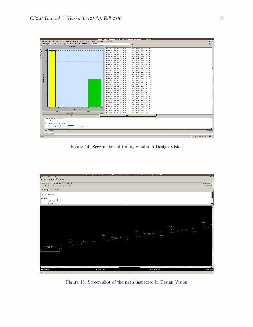
You can use Design Vision to examine various timing data. The Timing > Paths Slack menuoption will create a histogram of the worst case timing paths in your design. You can use thishistogram to gain some intuition on how to approach a design which does not meet timing. If thereare a large number of paths which have a very large negative timing slack then a global solution isprobably necessary, while if there are just one or two paths which are not making timing a morelocal approach may be sufficient. You can click on a bin and the tool will report critical pathsin the bin. Figure 14 shows an example of using these two features. Go ahead and right click tochoose Path Inspector. Figure 15 shows the actual components on the critical path.
It is sometimes useful to examine the critical path through a single submodule. To do this, rightclick on the module in the hierarchy view and use the Characterize option. Check the timing,constraints, and connections boxes and click OK. Now choose the module from the drop down listbox on the toolbar (called the Design List). Choosing Timing > Report Timing Path will provideinformation on the critical path through that submodule given the constraints of the submodulewithin the overall design’s context.
Fore more information on Design Vision consult the Design Vision User Guide (dc dv-user-guide.pdf).
CS250 Tutorial 5 (Version 091210b), Fall 2010 19
Figure 14: Screen shot of timing results in Design Vision
Figure 15: Screen shot of the path inspector in Design Vision

CS250 Tutorial 5 (Version 091210b), Fall 2010 20
Review
The following sequence of commands will setup the CS250 toolflow, checkout the RISC-V v1 pro-cessor example, and synthesize the design.
% source ~cs250/tools/cs250.bashrc
% mkdir tut5
% cd tut5
% TUTROOT=$PWD
% cp -R ~cs250/examples/v-riscv-v1-1stage/* $TUTROOT
% cd $TUTROOT/build/dc-syn
% make
Acknowledgements
Many people have contributed to versions of this tutorial over the years. The tutorial was origi-nally developed for CS250 VLSI Systems Design course at University of California at Berkeley byYunsup Lee. Contributors include: Krste Asanovic, Christopher Batten, John Lazzaro, and JohnWawrzynek. Versions of this tutorial have been used in the following courses:
• CS250 VLSI Systems Design (2009-2010) - University of California at Berkeley
• 6.375 Complex Digital Systems (2005-2009) - Massachusetts Institute of Technology
• CSE291 Manycore System Design (2009) - University of California at San Diego


![GCC internals intro y optimizationesnicolasw/Docencia/CP/gcc_int_intro.pdf · Optimizaciones Back-end Backend: – RTL tree + RTL language + RTL Engine + RTL Compiler [Middle-End]](https://img.dokumen.tips/doc/110x75/5f066be67e708231d417e97b/gcc-internals-intro-y-optimizationes-nicolaswdocenciacpgccintintropdf-optimizaciones.jpg)