Embed Size (px)
Citation preview

RTE-2000H-TP
Hardware User's Manual(Rev.1.02)
RealTimeEvaluator

RTE-2000H-TP Hardware User's Manual (Rev.1.02)
1
Notice * The copyright associated with this document is proprietary to Midas Lab. Co., Ltd.
* This document is protected under applicable copyright laws, and may not be copied,
redistributed or modified in whole or in part, in any way without explicit prior written permission
from Midas Lab. Co., Ltd.
* While this product was manufactured with all possible care, Midas Lab. Co., Ltd. and its
distributor assume no responsibility whatsoever for any result of using the product.
* The contents and specifications described in this document are subject to change without
notice.
Trademarks * MS-Windows, Windows, MS and MS-DOS are the trademarks of Microsoft Corporation,
U.S.A.
* The names of the programs, systems, CPUs, and other products that appear in this document
are usually trademarks of the manufacturer of the corresponding product.

RTE-2000H-TP Hardware User's Manual (Rev.1.02)
2
REVISION HISTORY
Rev.1.02 2006/04/05 Initial Revision

RTE-2000H-TP Hardware User's Manual (Rev.1.02)
3
目次
1. OVERVIEW ........................................................................................................................ 5 2. MAIN FEATURES ............................................................................................................. 6 3. HARDWARE SPECIFICATIONS OF MAJOR MODULES............................................. 7 4. COMPONENT NAMES AND FUNCTIONS .................................................................... 9 5. EXT CONNECTOR .......................................................................................................... 11 6. INSTALLATION PROCEDURE ..................................................................................... 13 7. CONNECTION TO THE USER SYSTEM...................................................................... 14 8. POWERING ON AND OFF ............................................................................................. 16 9. JTAG PROBE: PB-JTAG-N-A36................................................................................... 17
CONVENTIONAL TYPE (KEL TYPE)........................................................................................... 17 <PIN ARRANGEMENT TABLE>................................................................................................... 17 HIGH-SPEED TYPE (MICTOR TYPE) ........................................................................................ 19 ELECTRICAL CONDITION .......................................................................................................... 21 JTAG SIGNAL TIMING .............................................................................................................. 22 TRACE SIGNAL TIMING ........................................................................................................... 23
10. JTAG PROBE: PB-JTAG-N48 .................................................................................... 24 ELECTRICAL CONDITION .......................................................................................................... 27 JTAG SIGNAL TIMING .............................................................................................................. 28 TRACE SIGNAL TIMING ........................................................................................................... 29
11. JTAG PROBE: PB-JTAG-A-A36................................................................................. 30 ELECTRICAL CONDITION .......................................................................................................... 32 JTAG SIGNAL TIMING .............................................................................................................. 33 TRACE SIGNAL TIMING ........................................................................................................... 34
12. HIGH SPEED DOWN LOAD PROBE: PB-HSDL-50 ................................................ 34 12. HIGH SPEED DOWN LOAD PROBE: PB-HSDL-50 ................................................ 35
INTERFACE SPECIFICATIONS .................................................................................................... 35 NOTES ON USE.......................................................................................................................... 35 ELECTRICAL CONDITIONS......................................................................................................... 36 READ CYCLE TIMING............................................................................................................... 37
13. STANDARD ROM CABLE: CBL-ROM16-2K ............................................................ 38 TYPE OF SIGNAL LINE............................................................................................................... 38 PIN ARRANGEMENT TABLE ....................................................................................................... 38 CONNECTORS ........................................................................................................................... 39 LAYOUT OF THE CONNECTORS (ON THE BOARD) ....................................................................... 39 REFERENCE OF THE SCHEMATIC .............................................................................................. 40 JINH1-JP................................................................................................................................ 40

RTE-2000H-TP Hardware User's Manual (Rev.1.02)
4
ELECTRICAL CONDITION .......................................................................................................... 41 READ CYCLE TIMING............................................................................................................... 42 WRITE CYCLE TIMING............................................................................................................. 43
14. DIP32-ROM ADAPTER (ADP-STD16-DIP32).............................................................. 44 15. DIP40/42-ROM ADAPTER ............................................................................................ 45
DIP40-ROM ADAPTER: ADP-STD16-DIP40 ....................................................................... 45 DIP42-ROM ADAPTER: ADP-STD16-DIP42 ....................................................................... 45
APPENDIX-A MOUNTING BOARD MODULE................................................................. 46 APPENDIX-B MOUNTING MEM MODULE..................................................................... 47 APPENDIX-C APPEARANCE OF CABLE......................................................................... 49
PB-JTAG-N-XX, PB-JTAG-A-XX ............................................................................................ 49 PB-JTAG-N48......................................................................................................................... 49 PB-HSDL-50 ........................................................................................................................... 49 STANDARD ROM CABLE (RTE-STD16-2K) ............................................................................. 49 STANDARD ROM CABLE (RTE-STD16-2K) ............................................................................. 50 DIP-32/40/42-ROM ADAPTER (ADP-STD16-DIP32/40/42) ................................................... 50

RTE-2000H-TP Hardware User's Manual (Rev.1.02)
5
1. OVERVIEW
RTE-2000H-TP is a general-purpose in-circuit emulator that is connected to JTAG. Because it can debug a real processor on-board, this in-circuit emulator supplies highly stable and transparent emulation functions. Its hardware consists of a main enclosure to which up to six boards can be mounted and boards that are modularized in function units. These boards can be used in any combination. Each board consists of re-programmable devices so that it supports future function expansion and eliminates differences between different processors.
KIT (KIT-xxxx-TP-H) is a package of information on the above hardware and control software and is available for each model of processor.
This product consists of one of several types of main enclosures of different configurations
and optional products. First check the contents of the carton box by referring to the product list attached, to see if any component is missing.
The configuration of this product is as follows: Model Description
RTE-2000H-TP-N-A36 Basic configuration of NEC/MICTOR38-IF (with LAN/USB-IF) Main enclosure + power supply + USB cable
PB-JTAG-N-A36 (with CBL-MICTOR38)
One of a Kit for NEC's CPU (RTE4WIN32, UM, License)
RTE-2000H-TP-A-A36 Basic configuration for ARM/MICTOR38-IF (with LAN/USB-IF) Main enclosure + power supply + USB cable
PB-JTAG-A-A36 (with CBL-MICTOR38) One of a Kit for ARM's CPU (RTE4WIN32, UM, License)
RTE-2000H-TP-IF-IE80 Basic configuration for IE's POD (with LAN/USB-IF) Main enclosure + power supply + IF-IE80 + USB cable
• When the grade of a JTAG probe is changed, -A36 at the end of its model changes to the specified product number.

RTE-2000H-TP Hardware User's Manual (Rev.1.02)
6
2. MAIN FEATURES
Processor on-board emulation functions implemented by the high-speed JTAG circuit Because a high-speed JTAG circuit is mounted and the CPU is controlled through JTAG entirely, user resources such as memory and interrupts can be opened, thereby enabling stable operation by real chips and highly transparent emulation at high speeds.
Real-time trace function implemented by the high-speed and large-capacity trace circuit The high-speed and large-capacity trace function is mounted to display execution history in the unit of instruction or source line according to branch information output from the CPU. Instruction execution in the cache can be analyzed. The time tag is provided to measure up to 30 hours and to display trace information of the optional external bus together.
High-speed and large-capacity ROM emulation functions
ROM of up to 128M bytes and with a 64-bit bus can be emulated. Available are DIP ROMs with 32 to 42 pins and cables and adapters supporting the expansion STD-16BIT-ROM connector (32M bytes max.) to emulate ROM mounted on a board. The access time is as short as 35 ns or less.
High-speed download function implemented by high-speed download probe RTE-2000H-TP provides the bus-connection-type dedicated probe to download a large capacity program in memory in the user system at high speeds. The standard probe is the 16-bit bus interface conforming to the expansion STD-16BIT-ROM connector IF.
Abundant optional products
The following optional products are provided (example): • Large-capacity and high-speed emulation memory • Synchronous-type-flash-supporting emulation memory • 24/48-bit width trace supporting probe • External bus trace unit • High-speed download probe (bus connection type)
Enabling multiple debugger selection
The following debuggers can be used. (Which debuggers can be used depends on the KIT.) • Dedicated debugger "Partner" • GHS's "MULTI" • NEC Electronics' "ID850NW"
Supporting a multi-core processor
In the multi-core processor, multiple cores can be debugged concurrently and synchronous control (synchronous execution, synchronous break, etc) among the debuggers is possible.
Others
• Supporting low voltage (supporting 1.2 V and higher) • The LAN/USB-IF is mounted as a standard (100M bps/480M bps)
Remark: Because part of the above description depends on the KIT, the description cannot
be applied some KITs.

RTE-2000H-TP Hardware User's Manual (Rev.1.02)
7
3. HARDWARE SPECIFICATIONS OF MAJOR MODULES JTAG-IF: PB-JTAG-x-A36
Interface JTAG/N-Wire, JTAG/ETM
Operation voltage 1.2V – 3.3V
Remarks: *1: The most recent information of the KIT support state can be checked from the home page (http://www.midas.co.jp/).
*2: The values depend on the processor and KIT types and various types of conditions. The performance is not assured.
High Speed Down Load Probe: PB-HSDL-50
Remark: *2: The values depend on the processor and KIT types and various types of conditions. The performance is not assured.
Target CPU NB85E/NU85E, V850E/ME2, V850E/MA3 AS85EP2, NA85E2, V850E2/ME3, V831/2
VR5432, VR5432, VR5500, VR7701 VR4122, 4131, 4181A
MIPS32/4kc ARM9/11, OMAP16/15xx, MP211…more (*1)
JTAG functions CPU operating frequency Not limited
JTAG-CLK (standard product: when PB-JTAG-x-A36 is used)
10K – 100MHz(*2)
Trace functions (Some functions depend on the processor specifications.)
Trace data bus width PB-JTAG-x-A36 PB-JTAG-N48
4-16 bits 24-48 bits
Trace memory capacity. The option specifications are enclosed by ().
36M-bit (up to 144M-bit)
Maximum trace clock frequency PB-JTAG-x-A36 (The specifications applied when options are used are parenthesized.) PB-JTAG-N48
333MHz (up to 400MHz)
200MHz
Time tag resolution/maximum time measurement. The option specifications are enclosed by ().
100nS/30H
Trace delay cycle specification Supported Trigger that can be set using execution address Supported Trigger setting by data access Supported Trigger setting by external signal Supported Disassembled trace data display in the unit of
instruction Supported
Pin mask functions Supported
High speed down load probe: 50-pin-IF Interface Conforms to the IF specifications of the expansion
STD-16BIT-ROM cable (50 pin). Maximum data transfer rate 8M bytes (approx.)/sec(*2)
Access time 25nS (Typ.) Bus width 16 bits
Operation voltage 1.2V - 3.3V

RTE-2000H-TP Hardware User's Manual (Rev.1.02)
8
E.MEM: RTE-EMEM-B8, RTE-MM-8M
Used as RAM Supported
Electrical condition LV-TTL, 5-V tolerance
Remarks: Up to four boards can be mounted (max. 128M bytes). Two boards are necessary for the 32-bit bus, and four boards are necessary for the 64-bit bus.
*3: The DC characteristics of the cable may not electrically match if the operation voltage is 2.3 V or less.
Host-IF: LAN/USB-IF
LAN-IF 100BaseTX (100M bps)
ROM emulation functions Memory capacity 32M bytes (max.)/board
Access time 35 ns (asynchronous burst cycle: 30 ns) *3 Operation voltage 1.8V – 3.3V
Unit of map function in block (USER/EMEM) 64k words Capacity of ROMs that can be emulated (bits) DIP-32pin-ROM (8-bit bus) 1M, 2M, 4M, 8M (27C010/020/040/080) DIP-40pin-ROM (16-bit bus) 1M, 2M, 4M (27C1028/2048/4096) DIP-42pin-ROM (16-bit bus) 8M, 16M (27C8000/16000) Expansion STD-16BIT-ROM (16-bit bus) 1M, 2M, 4M, 8M, 16M, 32M, 64M, 128M, 256M (max. 32M bytes) Bus width specification (bits) 8/16/32/64
Host-IF USB-IF USB 2.0: Supports high-speed USB (480M bps)

RTE-2000H-TP Hardware User's Manual (Rev.1.02)
4. COMPONENT NAMES AND FUNCTIONS
This chapter shows the appearance of RTE-2000H-TP, as well as the names and functions of its components. (The photographs below show the IF-IE80 board mounted to RTE-2000H-TP-x-x.)
<Front view>
• Slots #1-#6 Slot #1
ICE-IF(60) board is mounted in thSlot #2
This slot is used to mount an optioon RTE-2000H-TP-IF-IE80 and dmount the board in this slot. Mou
Slots #3-#6 These slots are used to mountboards to these slots, starting from
• ICE-IF(60) board module (slot #1)ICE-IF(60)
60-pin connector to connect the PHSDL-IF
Connector to connect the high spe
Do not connthe HSDL-IF.
POWER (SW/LED) Power switch with LED. Turns oThe LED lights for ON.
LEDs (right) USER: Lights when power is suBUSY: Lights when communica
LEDs (left) READY: Lights when communicUSER: Lights when power is su
SW1/2
Slot #1
Slot #2
Slot #3
Slot #5
Slot #4
Slot #6
USB-IFLAN-IF HOST-IF
ICE-IF(80)
ICE-IF(60)
<Rear view> FHSDL-I
9
is slot (factory-set condition for shipment).
n module. The ICE-IF(80) board (IF-IE80) is mounted elivered. If this board is mounted later, be sure to nt an external bus trace board to this slot also.
emulation memory boards. Sequentially mount the the lowest slot, #3.
B-JTAG-x-xx
ed down load probe ect cables not specified (such as LAN) to Both of the products get faulty.
n and off repeatedly each time the button is pressed.
pplied to the user system connected via JTAG-IF. tion is carried out via JTAG-IF.
ation with HSDL-IF is carried out normally. pplied to the user system connected via HSDL-IF.

RTE-2000H-TP Hardware User's Manual (Rev.1.02)
10
• ICE-IF(80) board module (slot #2)
ICE-IF(80) 80-pin connector to connect the POD type ICE (IE)
EXT EXT connector enabled only when the ICE is connected to ICE-IF(80)
• E.MEM board module (slots #3-#6) E.ROM IF
Connector to connect the ROM cable D0-D7(LED)
Lights when power is supplied to the user system connected to the in-circuit emulator via the ROM cable.
D8-D15(LED) Lights when power is supplied to the user system connected to the in-circuit emulator via the ROM cable.
These two LEDs light at the same time when a 16-bit cable isconnected and when ADP-STD16-DIP32 is used.
Mount E.MEM board modules upward starting from slot #3. Thecorrespondence between the numbers of the ROMx commandsand modules is as follows:
ROM1 command … EMEM board module mounted into slot #3ROM2 command … EMEM board module mounted into slot #4ROM3 command … EMEM board module mounted into slot #5ROM4 command … EMEM board module mounted into slot #6
• Power jack (5 V) This is a connector for the power supply. Insert the supplied power plug.
Do not connect any device other than the supplied AC adapter(RTE-PS04: +5 V, 4.5 A) to the power jack.
• LAN/USB connectors (LAN/USB) These connectors are used for connecting RTE-2000H-TP to the PC (host system) via LAN or the USB IF. Connect either of them.
• PC (host) connector (HOST IF) This connector is used for connecting RTE-2000H-TP to the PC (host system), using the mounted host card. Connect no cable to this connector when connecting RTE-2000H-TP via LAN or USB.
• Switch for setting mode SW1, SW2
These switches are used to set modes of the ICE and emulation function. By referring to the manual of KIT-xxxx-TP, set these switches to "OFF" unless otherwise specified.

RTE-2000H-TP Hardware User's Manual (Rev.1.02)
11
5. EXT CONNECTOR The specifications of the JEXT1/2 mounted on the end of the JTAG probe and the EXT connector on the front panel of the ICE-IF(80) board (IF-IE80) are shown below. The ICE-IF(80) board connector is enabled only when the ICE is connected to the ICE-IF(80) connector. EXT connector of the JTAG probe (PB-JTAG-N-xx, PB-JTAG-A-xx)
JEXT1 Signal name I/O Description
1 GND --- Signal ground
2 EXI0 Input External input signal #0 (pulled up with 470 kΩ), edge-detectable
3 EXI1 Input External input signal #1 (pulled up with 470 kΩ)
4 EXI2 Input External input signal #2 (pulled up with 470 kΩ)
5 EXI3 Input External input signal #3 (pulled up with 470 kΩ)
JEXT2 Signal name I/O Description
1 RSV-IN0 Input Depends on KIT (pulled up with 470 kΩ)
2 RSV-IN1 Input Depends on KIT (pulled up with 470 kΩ)
3 RESETOUT- Output Reset output. Outputs a low pulse of about 50 ms in response to
the RESET command (open-collector output, pulled up with 470
kΩ).
4 TRG- Output Trigger output. Goes low when a trace trigger is detected
(open-collector output, pulled up with 470 kΩ).
5 RSV-OUT Output Depends on KIT (pulled up with 470 kΩ)
Remark: The I/O part is a 2-mm pitch plug. When using the signals, extract them by using a clip or the like used for logical analysis.
EXT connector of the ICE-IF(80) board
Pin No. (top) Signal name I/O Description
A1 RSV-IN0 Input Depends on KIT (pulled up with 1 kΩ)
A2 RSV-IN1 Input Depends on KIT (pulled up with 1 kΩ)
A3 RSV-OUT Output Depends on KIT (pulled up with 1 kΩ)
A4 RESETOUT- Output Reset output. Outputs a low pulse of about 50 ms in response to
the RESET command (open-collector output, pulled up with 1 kΩ).
A5 GND -- Signal ground
Pin No. (bottom) Signal name I/O Description
B1 EXI0 Input External input signal #0 (pulled up with 1 kΩ), edge-detectable
B2 EXI1 Input External input signal #1 (pulled up with 1 kΩ)
B3 EXI2 Input External input signal #2 (pulled up with 1 kΩ)
B4 EXI3 Input External input signal #3 (pulled up with 1 kΩ)
B5 TRG- Output Trigger output. Goes low when a trace trigger is detected
(open-collector output, pulled up with 1 kΩ).

RTE-2000H-TP Hardware User's Manual (Rev.1.02)
12
Pin arrangement
15 4 3 2
15 4 3 2
String A
String B
JEXT pin arrangement
Applicable connector 10-pin connector: OMRON XG4M-1031 (or equivalent) 1-pin jumper cable: ITT Pomona Electronics 4741-12-0 (or equivalent)
Supplement
1. The electrical condition of the input signals of the ICE-IF(80) board is LV-TTL level. 2. EXI0 can be detected at the edge as a trace trigger. 3. EXI0 to EXI3 are loaded to memory as trace information. 4. The signals are pulled up to the same voltage as -VCCIO of JTAG-IF.

RTE-2000H-TP Hardware User's Manual (Rev.1.02)
13
6. INSTALLATION PROCEDURE This chapter describes the procedure for installing RTE-2000H-TP.
1. Mount the host card. → When using the host card, mount it, referring to its corresponding manual.
2. Install RTE for WIN32. → For information, refer to the manual provided with RTE for WIN32.
At this point, do not start ChkRTE2.EXE.
3. Install RTE-2000H-TP. → The option module is mounted as a factory-set condition for shipment. If an additional
module is necessary, mount it by referring to Appendix A.
4. Connect RTE-2000H-TP. Connect RTE-2000H-TP and the PC (host system) to enable the AC adapter to be connected.
5. Connect RTE-2000H-TP to the user system. → Connect a JTAG probe applicable to the processor to the RTE-2000H-TP main
enclosure. Then connect the probe end to the user system. When using the optional end cable, replace the supplied cable with the optional cable. → For details, see Chapter 7.
6. Turn on the power. → For details, see Chapter 8.
7. Set RTE for WIN32. Start ChkRTE2.EXE and set the necessary parameters. → For details, refer to the manual provided with RTE for WIN32 or each KIT-xxxx-TP-H
manual.
8. Run the debugger. → Refer to the manual provided with the debugger.
The following figure shows an example of how the devices are connected.
Vxxx
PC
User system connection POD and cable (JTAG-IF and ROM cable)
AC adapter
RTE-2000H-TP CPU
ROM socket or connector
JTAG connector
User system
RTE-2000H-TP Hardware User's Manual (Rev.1.02)
14
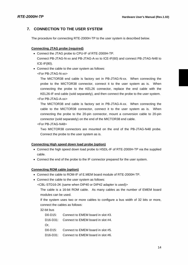
7. CONNECTION TO THE USER SYSTEM
The procedure for connecting RTE-2000H-TP to the user system is described below.
Connecting JTAG probe (required) • Connect the JTAG probe to CPU-IF of RTE-2000H-TP. Connect PB-JTAG-N-xx and PB-JTAG-A-xx to ICE-IF(60) and connect PB-JTAG-N48 to
ICE-IF(80). • Connect the cable to the user system as follows:
<For PB-JTAG-N-xx> The MICTOR38 end cable is factory set in PB-JTAG-N-xx. When connecting the probe to the MICTOR38 connector, connect it to the user system as is. When connecting the probe to the KEL26 connector, replace the end cable with the KEL26-IF end cable (sold separately), and then connect the probe to the user system.
<For PB-JTAG-A-xx> The MICTOR38 end cable is factory set in PB-JTAG-A-xx. When connecting the cable to the MICTOR38 connector, connect it to the user system as is. When connecting the probe to the 20-pin connector, mount a conversion cable to 20-pin connector (sold separately) on the end of the MICTOR38 end cable.
<For PB-JTAG-N48> Two MICTOR38 connectors are mounted on the end of the PB-JTAG-N48 probe. Connect the probe to the user system as is.
Connecting High speed down load probe (option) • Connect the high speed down load probe to HSDL-IF of RTE-2000H-TP via the supplied
cable. • Connect the end of the probe to the IF connector prepared for the user system.
Connecting ROM cable (option) • Connect the cable to ROM-IF of E.MEM board module of RTE-2000H-TP. • Connect the cable to the user system as follows:
<CBL-STD16-2K (same when DIP40 or DIP42 adapter is used)> The cable is a 16-bit ROM cable. As many cables as the number of EMEM board modules can be used. If the system uses two or more cables to configure a bus width of 32 bits or more, connect the cables as follows: 32-bit bus
D0-D15: Connect to EMEM board in slot #3. D16-D31: Connect to EMEM board in slot #4. Or, D0-D15: Connect to EMEM board in slot #5. D16-D31: Connect to EMEM board in slot #6.

RTE-2000H-TP Hardware User's Manual (Rev.1.02)
15
64-bit bus D0-D15: Connect to EMEM board in slot #3. D16-D31: Connect to EMEM board in slot #4. D32-D47: Connect to EMEM board in slot #5. D48-D63: Connect to EMEM board in slot #6.
<ADP-STD-DIP32> Attach the adapter for 8-bit, DIP-32-pin ROM to an end of CBL-STD16-2K. As many adapters as the number of EMEM board modules can be used. If the system uses two or more cables to configure a bus width of 16 bits or more, connect the adapter as follows: 16-bit bus
D0-D7: Connect to EMEM board in slot #3. D8-D15: Connect to EMEM board in slot #4. Or, D0-D7: Connect to EMEM board in slot #5. D8-D15: Connect to EMEM board in slot #6.
32-bit bus D0-D7: Connect to EMEM board in slot #3. D8-D16: Connect to EMEM board in slot #4. D16-D23: Connect to EMEM board in slot #5. D24-D31: Connect to EMEM board in slot #6.
Two types of pin assignments are used for a 32-pin ROM of 1M bit or more. Set the jumper on the adapterboard in accordance with the ROM to be used.

RTE-2000H-TP Hardware User's Manual (Rev.1.02)
16
8. POWERING ON AND OFF The procedures for powering the system on and off are described below. Complete all the steps in the installation procedure (such as cable connection) before powering the system on. Powering on
1. Turn on the power to the host system.
2. Turn on the power to RTE-2000H-TP. There are the following two methods:
• Connect the dedicated AC adapter to the power jack of RTE-2000H-TP.
Connecting the AC adapter turns on the power automatically at once.
• After the power is turned off by the POWER SW, pressing the POWER SW
again turns on the power.
3. Turn on the power to the user system.
4. Start the debugger. Powering off
1. Quit the debugger.
2. Turn off the power to the user system.
3. Turn off the power to RTE-2000H-TP. There are the following two methods:
• Disconnect the AC adapter from RTE-2000H-TP.
• Press the POWER SW on the front panel once.
4. Turn off the power to the host system according to the system procedure.
Do not turn on the power to the user system beforepowering on RTE-2000H-TP. Doing so may cause amalfunction.

RTE-2000H-TP Hardware User's Manual (Rev.1.02)
17
9. JTAG PROBE: PB-JTAG-N-A36
PB-JTAG-N-xx is a JTAG probe used to perform ICE for an NEC's CPU. The common specifications of this cable are shown below. Some signals are defined for an individual processor. When using the connectors, therefore, be sure to refer to the documents of each kit.
Conventional type (KEL type) The specifications of the interface using the conventional KEL type 26-pin connector are shown below. Use of a high-speed type connector is recommended if the specifications of a high-speed type are shown in KIT-xxxx-TP-H.
<Pin arrangement table>
Remark: I/O (user side) is the signal flow viewed at the user board side.
Pin
number
Connected
signal name
Input/output (user side) Standard treatment (user side)
A1 TRCCLK Output 22-33 Ω series resistor (recommended)
A2 TRCDATA0 Output 22-33 Ω series resistor (recommended)
A3 TRCDATA1 Output 22-33 Ω series resistor (recommended)
A4 TRCDATA2 Output 22-33 Ω series resistor (recommended)
A5 TRCDATA3 Output 22-33 Ω series resistor (recommended)
A6 TRCEND Output 22-33 Ω series resistor (recommended)
A7 DDI Input 4.7-10 kΩ pull-up or pull-down
A8 DCK Input 4.7-10 kΩ pull-up or pull-down
A9 DMS Input 4.7-10 kΩ pull-up or pull-down
A10 DDO Output 22-33 Ω series resistor (recommended)
A11 DRST- Input 4.7-50 kΩ pull-down
A12 Reserve ------ (Depends on KIT)
A13 Reserve ------ (Depends on KIT)
Pin
number
Connected
signal name
Input/output (user side) Treatment (user side)
B1-B10 GND ------ Connection to GND
B11 Reserve ------ (Depends on KIT)
B12 Reserve ------ (Depends on KIT)
B13 VCCIO ------ Connect to the power supply for the CPU external
bus.

RTE-2000H-TP Hardware User's Manual (Rev.1.02)
18
<Connectors> Manufacturer: KEL Models: 8830E-026-170S (straight) 8830E-026-170L (right angle) 8831E-026-170L (right angle, fixing hardware attached)
<Wiring and wire length>
1. Keep the wire from the buffer or CPU to the connector as short as possible. 100 mm or shorter is recommended.
2. Output signals from the CPU are recommended to be connected to connectors, via high-speed CMOS buffers of which power supply is the same as for CPU I/O buffers.
<Layout of the connectors on the board> The figure below shows the physical layout of the connectors on the board.
Board end [Top view ]
B13 A13 B12 A12
B2 A2 B1 A1
Polarity indication
Caution: When actually arranging the pins, design them according to the connector
dimensional information.
RTE-2000H-TP Hardware User's Manual (Rev.1.02)
19
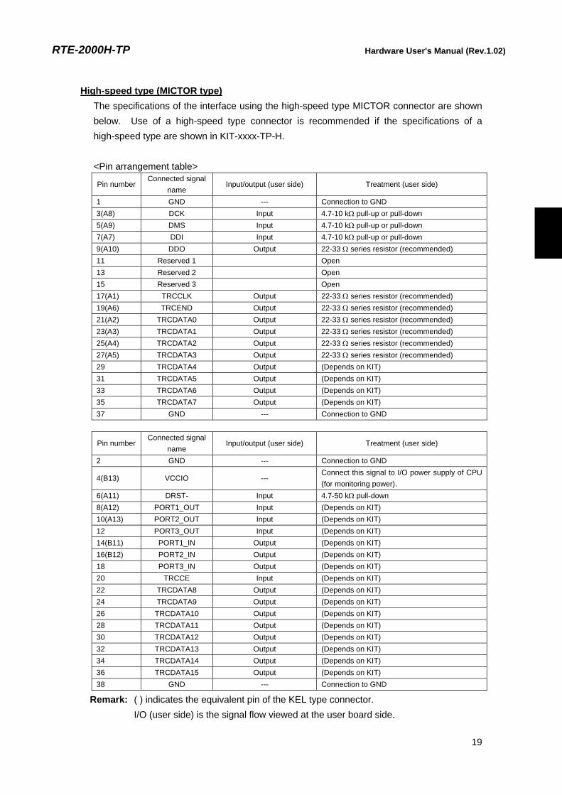
High-speed type (MICTOR type) The specifications of the interface using the high-speed type MICTOR connector are shown below. Use of a high-speed type connector is recommended if the specifications of a high-speed type are shown in KIT-xxxx-TP-H. <Pin arrangement table>
Pin number Connected signal
name Input/output (user side) Treatment (user side)
1 GND --- Connection to GND 3(A8) DCK Input 4.7-10 kΩ pull-up or pull-down 5(A9) DMS Input 4.7-10 kΩ pull-up or pull-down 7(A7) DDI Input 4.7-10 kΩ pull-up or pull-down 9(A10) DDO Output 22-33 Ω series resistor (recommended) 11 Reserved 1 Open 13 Reserved 2 Open 15 Reserved 3 Open 17(A1) TRCCLK Output 22-33 Ω series resistor (recommended) 19(A6) TRCEND Output 22-33 Ω series resistor (recommended) 21(A2) TRCDATA0 Output 22-33 Ω series resistor (recommended) 23(A3) TRCDATA1 Output 22-33 Ω series resistor (recommended) 25(A4) TRCDATA2 Output 22-33 Ω series resistor (recommended) 27(A5) TRCDATA3 Output 22-33 Ω series resistor (recommended) 29 TRCDATA4 Output (Depends on KIT) 31 TRCDATA5 Output (Depends on KIT) 33 TRCDATA6 Output (Depends on KIT) 35 TRCDATA7 Output (Depends on KIT) 37 GND --- Connection to GND
Pin number Connected signal
name Input/output (user side) Treatment (user side)
2 GND --- Connection to GND
4(B13) VCCIO --- Connect this signal to I/O power supply of CPU (for monitoring power).
6(A11) DRST- Input 4.7-50 kΩ pull-down 8(A12) PORT1_OUT Input (Depends on KIT) 10(A13) PORT2_OUT Input (Depends on KIT) 12 PORT3_OUT Input (Depends on KIT) 14(B11) PORT1_IN Output (Depends on KIT) 16(B12) PORT2_IN Output (Depends on KIT) 18 PORT3_IN Output (Depends on KIT) 20 TRCCE Input (Depends on KIT) 22 TRCDATA8 Output (Depends on KIT) 24 TRCDATA9 Output (Depends on KIT) 26 TRCDATA10 Output (Depends on KIT) 28 TRCDATA11 Output (Depends on KIT) 30 TRCDATA12 Output (Depends on KIT) 32 TRCDATA13 Output (Depends on KIT) 34 TRCDATA14 Output (Depends on KIT) 36 TRCDATA15 Output (Depends on KIT) 38 GND --- Connection to GND
Remark: ( ) indicates the equivalent pin of the KEL type connector. I/O (user side) is the signal flow viewed at the user board side.

RTE-2000H-TP Hardware User's Manual (Rev.1.02)
20
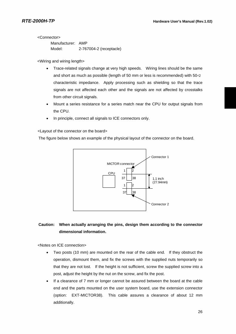
<Connector> Manufacturer: AMP Model: 2-767004-2 (receptacle)
<Wiring and wiring length>
• Trace-related signals change at very high speeds. Wiring lines should be the same
and short as much as possible (length of 50 mm or less is recommended) with 50-Ω
characteristic impedance. Apply processing such as shielding so that the trace
signals are not affected each other and the signals are not affected by crosstalks
from other circuit signals.
• Mount a series resistance for a series match near the CPU for output signals from
the CPU.
• In principle, connect all signals to ICE connectors only. <Layout of the connector on the board>
The figure below shows an example of the physical layout of the connector on the board.
CPU MICTOR connector
1 2
38 37 ICE connection direction
Caution: When actually arranging the pins, design them according to the connector
dimensional information.

RTE-2000H-TP Hardware User's Manual (Rev.1.02)
21
Electrical condition
Absolute Maximum Ratings Parameter Symbol Rating Unit
Supply voltage VDD -0.5-+5.5 V
Input voltage VI -0.5-+5.5 V
Note: The VDD is power voltage on target( = VCCIO of JTAG-IF)
Capacitance (TA=25°C)
Parameter Symbol MIN TYP MAX Unit
Input capacitance CI 50 ρF Output capacitance Co 50 ρF
DC Characteristics (1.2V<VDD<=5.5V) :VDD = VCCIO of JTAG-IF Condition Parameter Symbol
VDD(V) MIN TYP MAX Unit
1.2-1.95 VDD x0.65 V 1.95-2.7 1.6 V Input Voltage high VIH 2.7-5.5 2 V 1.2-1.95 VDD x0.35 V 1.95-2.7 0.7 V Input Voltage low VIL 2.7-5.5 0.8 V
1.2-3.2 VDD-0.2 V IOH = -100µA 3.3-5.5 3.0
IOH = -3mA 1.2 0.95 V IOH = -6mA 1.4 1.05 V IOH = -8mA 1.65 1.2 V IOL = -9mA 2.3 1.75 V
Output Voltage high VOH
IOL = -12mA 3.0 2.3 V IOH = -100µA 1.2-5.5 0.2 V IOH = -3mA 1.2 0.15 V IOH = -6mA 1.4 0.35 V IOH = -8mA 1.65 0.45 V IOL = -9mA 2.3 0.55 V
Output Voltage low
VOL
IOL = -12mA 3.0 0.7 V 1.2 -3 mA 1.4-1.6 -6 mA 1.65-1.95 -8 mA 2.3-2.7 -9 mA
Output current high IOH
3.0-5.5 -12 mA 1.2 3 mA 1.4-1.6 6 mA 1.65-1.95 8 mA 2.3-2.7 9 mA
Output current low IOL
3.0-5.5 12 mA VCCIO current IVCCIO 5.0 5 mA

RTE-2000H-TP Hardware User's Manual (Rev.1.02)
22
JTAG signal timing
Timing diagram
DCK
Valid DD O
Valid
t6 t5
t4
DMS, DDI
t1
t2 t3
DRS T
t7
AC Characteristics VDD = VCCIO of JTAG-IF
Parameter Symbol VDD (V) Min Typ. Max Unit Remarks
DCK Cycle Width t1 1.2-3.3 10 nS
DCK Cycle Low Width t2 1.2-3.3 0.4 * t1 nS
DCK Cycle High Width t3 1.2-3.3 0.4 * t1 nS
3.3 4.5 Tdly:DCK->DDI,DMS t4
1.2 5
nS
3.3 6.5 Tsu:DDO/DCK↓ t5
1.2 7.5
nS
3.3 0 Thold:DDO/DCK↓ t6
1.2 0
nS
DRST Low Width t7 1.2-3.3 1000 nS
AC input waveforms
Load condition
ICE C=15pF
1/2 1/2TEST POINTVdd
VSS

RTE-2000H-TP Hardware User's Manual (Rev.1.02)
23
TRACE signal timing
<Single Edge Mode>
Timing diagram
t4
TRCCLK
TRCDA TAx
t5
Valid
t1
t2 t3
TRCEND
AC Characteristics (1.2V<VDD<=3.3V):VDD = VCCIO of JTAG-IF Parameter Symbol Min Max Unit Remarks
TRCCLK Cycle Width t1 3 nS TRCCLK Cycle Low Width t2 1 nS TRCCLK Cycle High Width t3 1 nS
Tsu:TRCDATA,../TRCCLK↑ t4 0.0/1.5/3.0/4.5 nS The value depends on the following parameter of the tdata_dly command: Off/small/medium/large
Thold:TRCDATA,../TRCCLK↑ t5 1.5/0.0/-1.5/-3.0 nS
<Double Edge Mode>
Timing diagram
t4
TRCCLK
TRCDA TAx
t5
Valid
t1
t2 t3
TRCEND
t4 t5
Valid
AC Characteristics (1.2V<VDD<=3.3V):VDD = VCCIO of JTAG-IF Parameter Symbol Min Max Unit Remarks
TRCCLK Cycle Width t1 6 nS TRCCLK Cycle Low Width t2 2 nS TRCCLK Cycle High Width t3 2 nS
Tsu:TRCDATA,../TRCCLK↑↓ t4 0.0/1.5/3.0/4.5 nS The value depends on the following parameter of the tdata_dly command: Off/small/medium/large
Thold:TRCDATA,../ TRCCLK↑↓ t5 1.5/0.0/-1.5/-3.0 nS
AC input waveforms
1/2 1/2TEST POINT
Vdd
VSS

RTE-2000H-TP Hardware User's Manual (Rev.1.02)
24
10. JTAG PROBE: PB-JTAG-N48
PB-JTAG-N48 is a probe, supporting a trace bus of up to 48 bits, is used to emulate NEC's CPUs. The common specifications of this probe are shown below. Some signals are defined for an individual processor. When preparing the connectors actually, be sure to refer to the documents of each kit. This cable supports some processors having multi-bit trace buses, therefore, refer to the manual of each kit to check if a processor is supported.
The interface specifications are shown below. <Pin arrangement table>
Connector 1
Pin number Connected signal
name Input/output (user side) Treatment (user side)
1 GND --- Connection to GND 3 DCK Input 4.7-10 kΩ pull-up or pull-down 5 DMS Input 4.7-10 kΩ pull-up or pull-down 7 DDI Input 4.7-10 kΩ pull-up or pull-down 9 DDO Output 22-33 Ω series resistor (recommended) 11 Reserved 1 Open 13 Reserved 2 Open 15 Reserved 3 Open 17 TRCCLK Output 22-33 Ω series resistor (recommended) 19 TRCEND Output 22-33 Ω series resistor (recommended) 21 TRCDATA0 Output 22-33 Ω series resistor (recommended) 23 TRCDATA1 Output 22-33 Ω series resistor (recommended) 25 TRCDATA2 Output 22-33 Ω series resistor (recommended) 27 TRCDATA3 Output 22-33 Ω series resistor (recommended) 29 TRCDATA4 Output (Depends on KIT) 31 TRCDATA5 Output (Depends on KIT) 33 TRCDATA6 Output (Depends on KIT) 35 TRCDATA7 Output (Depends on KIT) 37 GND --- Connection to GND
Pin number Connected signal
name Input/output (user side) Treatment (user side)
2 GND --- Connection to GND
4 VCCIO --- Connect this signal to I/O power supply of CPU (for monitoring power).
6 DRST- Input 4.7-50 kΩ pull-down 8 PORT1_OUT Input (Depends on KIT) 10 PORT2_OUT Input (Depends on KIT) 12 PORT3_OUT Input (Depends on KIT) 14 PORT1_IN Output (Depends on KIT) 16 PORT2_IN Output (Depends on KIT) 18 PORT3_IN Output (Depends on KIT) 20 TRCCE Input (Depends on KIT) 22 TRCDATA8 Output (Depends on KIT) 24 TRCDATA9 Output (Depends on KIT) 26 TRCDATA10 Output (Depends on KIT) 28 TRCDATA11 Output (Depends on KIT) 30 TRCDATA12 Output (Depends on KIT) 32 TRCDATA13 Output (Depends on KIT) 34 TRCDATA14 Output (Depends on KIT) 36 TRCDATA15 Output (Depends on KIT) 38 GND --- Connection to GND

RTE-2000H-TP Hardware User's Manual (Rev.1.02)
25
Connector 2 Pin number
Connected signal name
Input/output (user side) Treatment (user side)
1 GND Connection to GND 3 TRCDATA16 Output 22-33 Ω series resistor (recommended) 5 TRCDATA17 Output 22-33 Ω series resistor (recommended) 7 TRCDATA18 Output 22-33 Ω series resistor (recommended) 9 TRCDATA19 Output 22-33 Ω series resistor (recommended) 11 TRCDATA20 Output 22-33 Ω series resistor (recommended) 13 TRCDATA21 Output 22-33 Ω series resistor (recommended) 15 TRCDATA22 Output 22-33 Ω series resistor (recommended) 17 TRCDATA23 Output 22-33 Ω series resistor (recommended) 19 TRCDATA24 Output 22-33 Ω series resistor (recommended) 21 TRCDATA25 Output 22-33 Ω series resistor (recommended) 23 TRCDATA26 Output 22-33 Ω series resistor (recommended) 25 TRCDATA27 Output 22-33 Ω series resistor (recommended) 27 TRCDATA28 Output 22-33 Ω series resistor (recommended) 29 TRCDATA29 Output 22-33 Ω series resistor (recommended) 31 TRCDATA30 Output 22-33 Ω series resistor (recommended) 33 TRCDATA31 Output 22-33 Ω series resistor (recommended) 35 --- --- Open 37 GND Connection to GND
Pin number
Connected signal name
Input/output (user side) Treatment (user side)
2 GND Connection to GND 4 TRCDATA32 Output 22-33 Ω series resistor (recommended) 6 TRCDATA33 Output 22-33 Ω series resistor (recommended) 8 TRCDATA34 Output 22-33 Ω series resistor (recommended) 10 TRCDATA35 Output 22-33 Ω series resistor (recommended) 12 TRCDATA36 Output 22-33 Ω series resistor (recommended) 14 TRCDATA37 Output 22-33 Ω series resistor (recommended) 16 TRCDATA38 Output 22-33 Ω series resistor (recommended) 18 TRCDATA39 Output 22-33 Ω series resistor (recommended) 20 TRCDATA40 Output 22-33 Ω series resistor (recommended) 22 TRCDATA41 Output 22-33 Ω series resistor (recommended) 24 TRCDATA42 Output 22-33 Ω series resistor (recommended) 26 TRCDATA43 Output 22-33 Ω series resistor (recommended) 28 TRCDATA44 Output 22-33 Ω series resistor (recommended) 30 TRCDATA45 Output 22-33 Ω series resistor (recommended) 32 TRCDATA46 Output 22-33 Ω series resistor (recommended) 34 TRCDATA47 Output 22-33 Ω series resistor (recommended) 36 --- --- Open 38 GND Output Connection to GND
Remark: I/O (user side) is the signal flow viewed at the user board side.
Connector 1 is compatible with the end of PB-JTAG-N-xx.
RTE-2000H-TP Hardware User's Manual (Rev.1.02)
26
<Connector> Manufacturer: AMP Model: 2-767004-2 (receptacle)
<Wiring and wiring length>
• Trace-related signals change at very high speeds. Wiring lines should be the same
and short as much as possible (length of 50 mm or less is recommended) with 50-Ω
characteristic impedance. Apply processing such as shielding so that the trace
signals are not affected each other and the signals are not affected by crosstalks
from other circuit signals.
• Mount a series resistance for a series match near the CPU for output signals from
the CPU.
• In principle, connect all signals to ICE connectors only. <Layout of the connector on the board>
The figure below shows an example of the physical layout of the connector on the board.
CPU
MICTOR connector
1 2
38 37
1 2
37 38
1.1 inch (27.94mm)
Connector 1
Connector 2
Caution: When actually arranging the pins, design them according to the connector
dimensional information.
<Notes on ICE connection>
• Two posts (10 mm) are mounted on the rear of the cable end. If they obstruct the
operation, dismount them, and fix the screws with the supplied nuts temporarily so
that they are not lost. If the height is not sufficient, screw the supplied screw into a
post, adjust the height by the nut on the screw, and fix the post.
• If a clearance of 7 mm or longer cannot be assured between the board at the cable
end and the parts mounted on the user system board, use the extension connector
(option: EXT-MICTOR38). This cable assures a clearance of about 12 mm
additionally.

RTE-2000H-TP Hardware User's Manual (Rev.1.02)
27
Electrical condition
Absolute Maximum Ratings
Parameter Symbol Rating Unit
Supply voltage VDD -0.5-+3.6 V
Input voltage VI -0.5-+3.6 V
Note: The VDD is power voltage on target( = VCCIO of JTAG-IF)
Capacitance (TA=25°C)
Parameter Symbol MIN TYP MAX Unit
Input capacitance CI 50 ρF
Output
capacitance Co 50 ρF
DC Characteristics 1.8V<VDD<=3.6V) :VDD = VCCIO of JTAG-IF Condition Parameter Symbol
VDD(V) MIN TYP MAX Unit
Input Voltage high VIH 1.7 5.5 V Input Voltage low VIL 0.7 V
IOH = -100µA VDD-0.2 V IOH = -4mA 1.8 1.2 V IOH = -8mA 2.3 1.75 V
Output Voltage high VOH
IOH = -12mA 3 2.3 V IOL = 100µA 0.2 V IOL = 4mA 1.65 0.45 V IOL = 8mA 2.3 0.55 V
Output Voltage low
VOL
IOL = 12mA 3.0 0.7 V 1.8-1.95 -4 mA 2.3-2.7 -8 mA Output current high IOH 3.0-3.6 -12 mA 1.8-1.95 4 mA 2.3-2.7 8 mA Output current low IOL 3.0-3.6 12 mA
VDD current IVDD 3.3 2.5 mA
RTE-2000H-TP Hardware User's Manual (Rev.1.02)
28
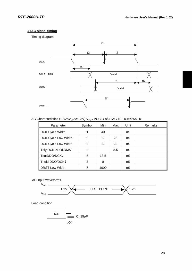
JTAG signal timing
Timing diagram
DCK
Valid DD O
Valid
t6 t5
t4
DMS, DDI
t1
t2 t3
DRS T
t7
AC Characteristics (1.8V<VDD<=3.3V):VDD = VCCIO of JTAG-IF, DCK=25MHz
Parameter Symbol Min Max Unit Remarks
DCK Cycle Width t1 40 nS
DCK Cycle Low Width t2 17 23 nS
DCK Cycle Low Width t3 17 23 nS
Tdly:DCK->DDI,DMS t4 8.5 nS
Tsu:DDO/DCK↓ t5 13.5 nS
Thold:DDO/DCK↓ t6 0 nS
DRST Low Width t7 1000 nS
AC input waveforms
Load condition
ICE C=15pF
1.25 1.25TEST POINTVdd
VSS

RTE-2000H-TP Hardware User's Manual (Rev.1.02)
29
TRACE signal timing
<Single Edge Mode>
Timing diagram
t4
TRCCLK
TRCDA TAx
t5
Valid
t1
t2 t3
TRCEND
AC Characteristics (1.8V<VDD<=3.3V):VDD = VCCIO of JTAG-IF Parameter Symbol Min Max Unit Remarks
TRCCLK Cycle Width t1 5 nS TRCCLK Cycle Low Width t2 2 nS TRCCLK Cycle High Width t3 2 nS
Tsu:TRCDATA,../TRCCLK↑ t4 2/3/4/5 nS The value depends on the following parameter of the tdata_dly command: Off/small/medium/large
Thold:TRCDATA,../TRCCLK↑ t5 0/-1/-2/-3 nS
<Double Edge Mode>
Timing diagram
t4
TRCCLK
TRCDA TAx
t5
Valid
t1
t2 t3
TRCEND
t4 t5
Valid
AC Characteristics (1.8V<VDD<=3.3V):VDD = VCCIO of JTAG-IF Parameter Symbol Min Max Unit Remarks
TRCCLK Cycle Width t1 10 nS TRCCLK Cycle Low Width t2 4 nS TRCCLK Cycle High Width t3 4 nS
Tsu:TRCDATA,../TRCCLK↑↓ t4 2/3/4/5 nS The value depends on the following parameter of the tdata_dly command: Off/small/medium/large
Thold:TRCDATA,../ TRCCLK↑↓ t5 0/-1/-2/-3 nS
AC input waveforms
1.25 1.25TEST POINT
Vdd
VSS

RTE-2000H-TP Hardware User's Manual (Rev.1.02)
30
11. JTAG PROBE: PB-JTAG-A-A36
PB-JTAG-A-xx is a JTAG probe that is used to emulate ARM-CPUs. The common specifications are shown below. Some signals are defined for an individual processor. When using the connectors, therefore, be sure to refer to the documents of each kit.
<Pin arrangement table>
Pin number Connected signal
name Input/output (user side) Treatment (user side)
1 NC. --- Not used 3 NC. --- Not used 5 Reserved --- Not used 7 DGBRQ Input 4.7-10 kΩ pull-down 9 nSRST Input 4.7-10 kΩ pull-up 11 TDO Output 22-33 Ω series resistor (recommended) 13 RTCLK Output 22-33 Ω series resistor (recommended) 15 TCK Input 4.7-10 kΩ pull-up or pull-down 17 TMS Input 4.7-10 kΩ pull-up or pull-down 19 TDI Input 4.7-10 kΩ pull-up or pull-down 21 nTRST Input 4.7-50 kΩ pull-down 23 TRACEPKT[15] Output 22-33 Ω series resistor (recommended) 25 TRACEPKT[14] Output 22-33 Ω series resistor (recommended) 27 TRACEPKT[13] Output 22-33 Ω series resistor (recommended) 29 TRACEPKT[12] Output 22-33 Ω series resistor (recommended) 31 TRACEPKT[11] Output 22-33 Ω series resistor (recommended) 33 TRACEPKT[10] Output 22-33 Ω series resistor (recommended) 35 TRACEPKT[9] Output 22-33 Ω series resistor (recommended) 37 TRACEPKT[8] Output 22-33 Ω series resistor (recommended)
Pin number Connected signal
name Input/output (user side) Treatment (user side)
2 NC. --- Not used 4 NC. --- Not used 6 TRACECLK Output 22-33 Ω series resistor (recommended) 8 DBGACK Output 22-33 Ω series resistor (recommended) 10 EXTTRIG Input Connecting this signal to unused interrupt input
is recommended (option). 12 VTRef Output Connect this signal to I/O power supply of CPU
(for monitoring power). 14 Vsuuply Output Connect this signal to I/O power supply of CPU
(not used by ICE). 16 TRACEPKT[7] Output 22-33 Ω series resistor (recommended) 18 TRACEPKT[6] Output 22-33 Ω series resistor (recommended) 20 TRACEPKT[5] Output 22-33 Ω series resistor (recommended) 22 TRACEPKT[4] Output 22-33 Ω series resistor (recommended) 24 TRACEPKT[3] Output 22-33 Ω series resistor (recommended) 26 TRACEPKT[2] Output 22-33 Ω series resistor (recommended) 28 TRACEPKT[1] Output 22-33 Ω series resistor (recommended) 30 TRACEPKT[0] Output 22-33 Ω series resistor (recommended) 32 TRACESYNC Output 22-33 Ω series resistor (recommended) 34 PIPSTAT[2] Output 22-33 Ω series resistor (recommended) 36 PIPSTAT[1] Output 22-33 Ω series resistor (recommended) 38 PIPSTAT[0] Output 22-33 Ω series resistor (recommended)

RTE-2000H-TP Hardware User's Manual (Rev.1.02)
31
<Connector> Manufacturer: AMP Model: 2-767004-2 (receptacle)
<Wiring and wiring length>
• Trace (ETM)-related signals change at very high speeds. Wiring lines should be
the same and short as much as possible (length of 50 mm or less is recommended)
with 50-Ω characteristic impedance. Apply processing such as shielding so that the
signals are not affected each other and the signals are not affected by crosstalks
from other circuit signals.
• Mount a series resistance for series match near the CPU for output signals from the
CPU.
• In principle, connect all signals to ICE connectors only.
• nSRST is a signal used for resetting a CPU. Set the signal so that it is ORed with
the signal that resets the CPU on the board. The signal is output from ICE by OC.,
so it can be wire-ORed if the reset request signal on the board is output by OC. <Board layout>
The figure below shows an example of the physical layout of the connector on the board.
CPU MICTOR connector
1 2
38 37 ICE connection direction
Caution: When actually arranging the pins, design them according to the connector
dimensional information.

RTE-2000H-TP Hardware User's Manual (Rev.1.02)
32
Electrical condition
Absolute Maximum Ratings Parameter Symbol Rating Unit
Supply voltage VDD -0.5-+3.6 V
Input voltage VI -0.5-+3.6 V
Note: The VDD is power voltage on target( = VCCIO of JTAG-IF)
Capacitance (TA=25°C)
Parameter Symbol MIN TYP MAX Unit
Input capacitance CI 50 ρF Output capacitance Co 50 ρF
DC Characteristics (1.2V<VDD<=3.6V) :VDD = VCCIO of JTAG-IF Condition Parameter Symbol
VDD(V) MIN TYP MAX Unit
1.2-1.95 VDD x0.65 V 1.95-2.7 1.6 V Input Voltage high VIH 2.7-5.5 2 V 1.2-1.95 VDD x0.35 V 1.95-2.7 0.7 V Input Voltage low VIL 2.7-3.6 0.8 V
1.2-3.2 VDD-0.2 V IOH = -100µA 3.3-3.6 3.0
IOH = -3mA 1.2 0.95 V IOH = -6mA 1.4 1.05 V IOH = -8mA 1.65 1.2 V IOL = -9mA 2.3 1.75 V
Output Voltage high VOH
IOL = -12mA 3.0 2.3 V IOH = -100µA 1.2-5.5 0.2 V IOH = -3mA 1.2 0.15 V IOH = -6mA 1.4 0.35 V IOH = -8mA 1.65 0.45 V IOL = -9mA 2.3 0.55 V
Output Voltage low
VOL
IOL = -12mA 3.0 0.7 V 1.2 -3 mA 1.4-1.6 -6 mA 1.65-1.95 -8 mA 2.3-2.7 -9 mA
Output current high IOH
3.0-3.6 -12 mA 1.2 3 mA 1.4-1.6 6 mA 1.65-1.95 8 mA 2.3-2.7 9 mA
Output current low IOL
3.0-3.6 12 mA VCCIO current IVCCIO 3.3 5 mA

RTE-2000H-TP Hardware User's Manual (Rev.1.02)
33
JTAG signal timing
Timing diagram
TCK
Valid TDO
Valid
t6 t5
t4
TMS, TD I
t1
t2 t3
nSRS T
t7
AC Characteristics VDD = VCCIO of JTAG-IF
Parameter Symbol VDD (V) Min Typ. Max Unit Remarks
DCK Cycle Width t1 1.2-3.3 10 nS Depends on RTCK.
DCK Cycle Low Width t2 1.2-3.3 0.4 * t1 nS Depends on RTCK.
DCK Cycle High Width t3 1.2-3.3 0.4 * t1 nS Depends on RTCK.
3.3 4.5 Tdly:DCK->DDI,DMS t4
1.2 5
nS
3.3 6.5 Tsu:DDO/DCK↓ t5
1.2 7.5
nS
3.3 0 Thold:DDO/DCK↓ t6
1.2 0
nS
DRST Low Width t7 1.2-3.3 1000 nS
AC input waveforms
Load condition
ICE C=15pF
1/2 1/2TEST POINTVdd
VSS

RTE-2000H-TP Hardware User's Manual (Rev.1.02)
34
TRACE signal timing
<Single Edge Mode>
Timing diagram
t4
TRACE CLK
TRACEPK T[]
t5
Valid
t1
t2 t3
PIPSTA T[]
AC Characteristics (1.2V<VDD<=3.3V):VDD = VCCIO of JTAG-IF Parameter Symbol Min Max Unit Remarks
TRACECLK Cycle Width t1 3 nS TRACECLK Cycle Low Width t2 1 nS TRACECLK Cycle High Width t3 1 nS
Tsu:TRCDATA,../TRACECLK↑ t4 -0.5/0.5/1.5/2.5 nS The value depends on the following parameter of the tdata_dly command: Off/small/medium/large
Thold:TRCDATA,../TRACECLK↑ t5 2.0/1.0/0.0/-1.0 nS
<Double Edge Mode>
Timing diagram
t4
TRACE CLK
TRACEPK T[]
t5
Valid
t1
t2 t3
PIPSTA T[]
t4 t5
Valid
AC Characteristics (1.2V<VDD<=3.3V):VDD = VCCIO of JTAG-IF Parameter Symbo
l Min Ma
x Unit Remarks
TRACECLK Cycle Width t1 6 nS TRACECLK Cycle Low Width t2 2 nS TRACECLK Cycle High Width t3 2 nS
Tsu:TRCDATA,./TRACECLK↑↓ t4 -0.5/0.5/1.5/2.5 nS The value depends on the following parameter of the tdata_dly command: Off/small/medium/large
Thold:TRCDATA,./TRACECLK↑↓ t5 2.0/1.0/0.0/-1.0 nS
AC input waveforms
1/2 1/2TEST POINTVdd
VSS
RTE-2000H-TP Hardware User's Manual (Rev.1.02)
35
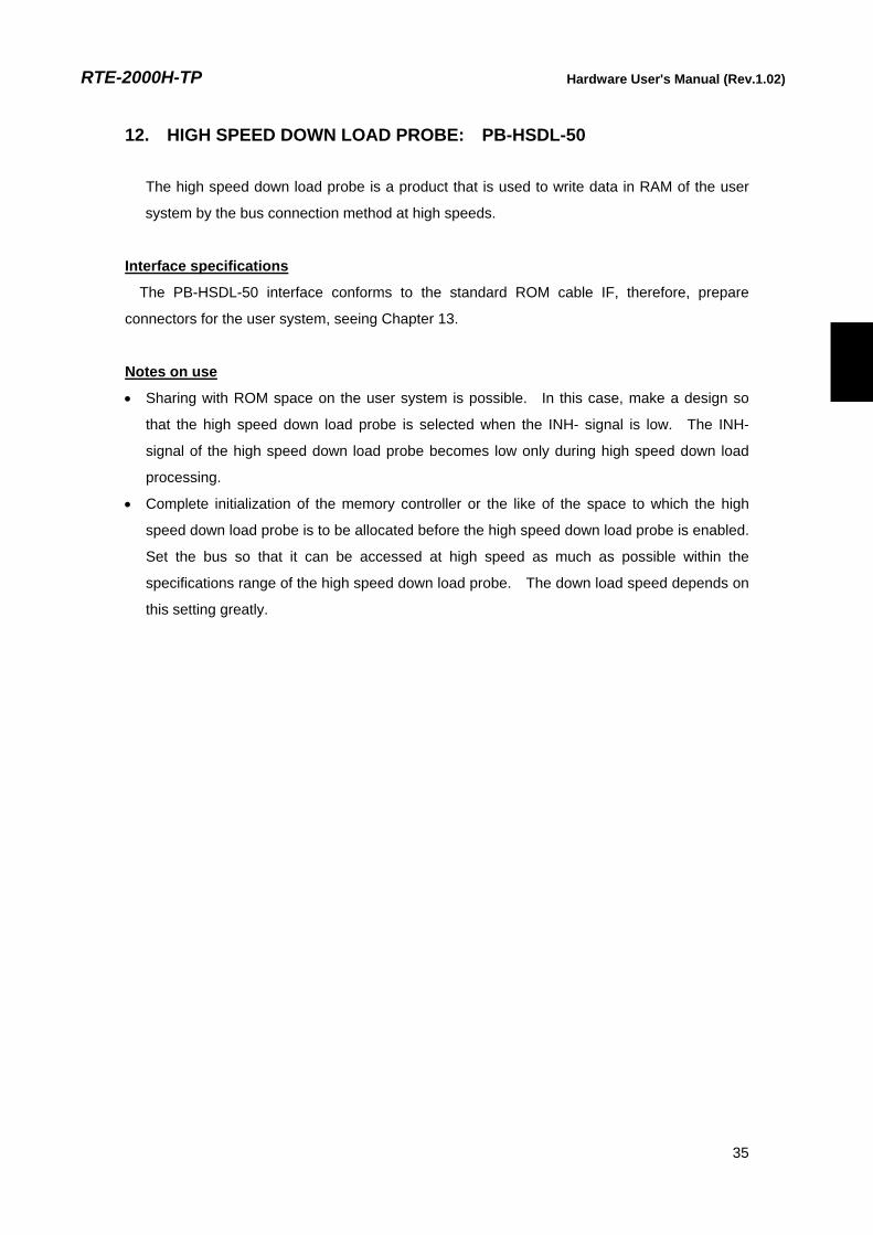
12. HIGH SPEED DOWN LOAD PROBE: PB-HSDL-50
The high speed down load probe is a product that is used to write data in RAM of the user
system by the bus connection method at high speeds.
Interface specifications
The PB-HSDL-50 interface conforms to the standard ROM cable IF, therefore, prepare
connectors for the user system, seeing Chapter 13.
Notes on use
• Sharing with ROM space on the user system is possible. In this case, make a design so
that the high speed down load probe is selected when the INH- signal is low. The INH-
signal of the high speed down load probe becomes low only during high speed down load
processing.
• Complete initialization of the memory controller or the like of the space to which the high
speed down load probe is to be allocated before the high speed down load probe is enabled.
Set the bus so that it can be accessed at high speed as much as possible within the
specifications range of the high speed down load probe. The down load speed depends on
this setting greatly.

RTE-2000H-TP Hardware User's Manual (Rev.1.02)
36
Electrical conditions
Absolute Maximum Ratings Parameter Symbol Rating Unit
Supply voltage VDD -0.5-+3.6 V
Input voltage VI -0.5-+3.6 V
Note: The VDD is power voltage on target( = VCCIO of JTAG-IF)
Capacitance (TA=25°C)
Parameter Symbol MIN TYP MAX Unit
Input capacitance CI 50 ρF Output capacitance Co 50 ρF
DC Characteristics (1.2V<VDD<=3.6V) :VDD = VCCIO of JTAG-IF Condition Parameter Symbol
VDD(V) MIN TYP MAX Unit
1.2-1.95 VDD x0.65 V 1.95-2.7 1.6 V Input Voltage high VIH 2.7-5.5 2 V 1.2-1.95 VDD x0.35 V 1.95-2.7 0.7 V Input Voltage low VIL 2.7-3.6 0.8 V
1.2-3.2 VDD-0.2 V IOH = -100µA 3.3-3.6 3.0
IOH = -3mA 1.2 0.95 V IOH = -6mA 1.4 1.05 V IOH = -8mA 1.65 1.2 V IOL = -9mA 2.3 1.75 V
Output Voltage high VOH
IOL = -12mA 3.0 2.3 V IOH = -100µA 1.2-5.5 0.2 V IOH = -3mA 1.2 0.15 V IOH = -6mA 1.4 0.35 V IOH = -8mA 1.65 0.45 V IOL = -9mA 2.3 0.55 V
Output Voltage low
VOL
IOL = -12mA 3.0 0.7 V 1.2 -3 mA 1.4-1.6 -6 mA 1.65-1.95 -8 mA 2.3-2.7 -9 mA
Output current high IOH
3.0-3.6 -12 mA 1.2 3 mA 1.4-1.6 6 mA 1.65-1.95 8 mA 2.3-2.7 9 mA
Output current low IOL
3.0-3.6 12 mA VCCIO current IVCCIO 3.3 5 mA
RTE-2000H-TP Hardware User's Manual (Rev.1.02)
37
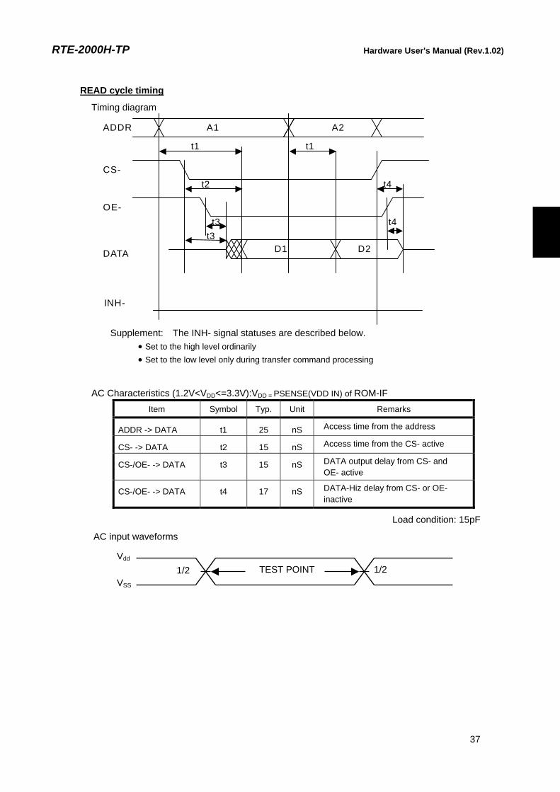
READ cycle timing
Timing diagram
t1
t2
t3 t4
t4
ADDR
CS-
OE-
DATA
t3
t1
A1 A2
D1 D2
INH-
Supplement: The INH- signal statuses are described below.
• Set to the high level ordinarily • Set to the low level only during transfer command processing
AC Characteristics (1.2V<VDD<=3.3V):VDD = PSENSE(VDD IN) of ROM-IF Item Symbol Typ. Unit Remarks
ADDR -> DATA t1 25 nS Access time from the address
CS- -> DATA t2 15 nS Access time from the CS- active
CS-/OE- -> DATA t3 15 nS DATA output delay from CS- and OE- active
CS-/OE- -> DATA t4 17 nS DATA-Hiz delay from CS- or OE- inactive
Load condition: 15pF
AC input waveforms
1/2 1/2TEST POINTVdd
VSS

RTE-2000H-TP Hardware User's Manual (Rev.1.02)
38
13. STANDARD ROM CABLE: CBL-ROM16-2K
This cable supports the STD-16BIT-ROM connector recommended by NEC. Usually, ROM can be emulated while mounted on a board by preparing this connector on the board. Adapters to be attached to the ends of this cable are available for ROM of DIP-40 and DIP-42.
Type of signal line Signal IN/OUT Name Description
A0-A23 IN ADDRESS BUS Connect address signals equivalent to those of ROM to these signals. • Connect the higher address signals that are not used to GND.• Connect the A1 signal of the CPU to A0 of the 16-bit bus. • Connect the A2 signal of the CPU to A0 of the 32-bit bus.
D0-D15 OUT DATA BUS Connect data signals equivalent to those of ROM to these signals.
CE- IN CHIP ENABLE ROM emulator is selected at LOW level.
OE- IN OUTPUT ENABLE If CE- is LOW and this signal is LOW, ROM emulator will output the data bus signals.
WRL- WRH-
IN Write low-byte Write High-byte
Connect a low-active write signal to this signal to write data to the emulation memory. Connecting a write signal is not essential, however. When this signal is not used, fix it to the high level.
PSENSE IN POWER SENSE Connect this signal to VDD on the ROM power supply (for monitoring power).
INH- OUT INHBIT- Use this signal to disable ROM on the board. The following two signals can be selected by selection of JINH1 . Side 1: Select GND. Always drive this signal low. Side 3: Select EMEMEN-. This signal outputs a low level only when the emulation memory is selected.
GND ----- GND Connect to GND on a board.
Pin arrangement table A side Signal B side Signal
A1 GND B1 A0 A2 A1 B2 A2 A3 A3 B3 A4 A4 A5 B4 A6 A5 A7 B5 A8 A6 A9 B6 A10 A7 A11 B7 A12 A8 A13 B8 A14 A9 A15 B9 A16
A10 A17 B10 A18 A11 A19 B11 A20 A12 A21 B12 A22 A13 (WRH-) B13 INH- (GND/EMEMEN-) A14 (WRL-) B14 A23 A15 CE- B15 GND A16 OE- B16 PSENSE (VDD IN) A17 D0 B17 D1 A18 D2 B18 D3 A19 D4 B19 D5 A20 D6 B20 D7 A21 D8 B21 D9 A22 D10 B22 D11 A23 D12 B23 D13 A24 D14 B24 D15 A25 GND B25 GND

RTE-2000H-TP Hardware User's Manual (Rev.1.02)
39
Connectors Manufacturer: KEL Models: 8931E-050-178S (straight)
8931E-050-178L (right angle)
8930E-050-178MS (SMT straight)
Layout of the connectors (on the board)
A1
B1B25
A25 1-pin mark
Edge of board
RTE-2000H-TP Hardware User's Manual (Rev.1.02)
40
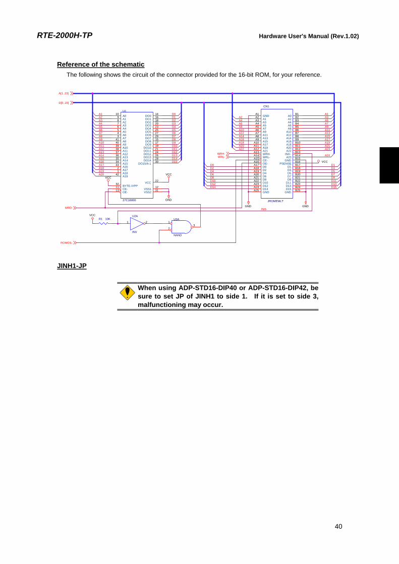
Reference of the schematic The following shows the circuit of the connector provided for the 16-bit ROM, for your reference.
D11
D13
D1
D15
A10
A2
D11
A17
A9
A3
D12
VCC
ROMCS-
A4 A6
A19A11
WRH-
D1
VCC
A14
A14A15
D7
A16
A18D4
A5
A13
A9D3
A22
VCC
A3A4
A16
A23
D2
WRL- A24
D0
U1
27C16000
12
14
22
31
32
1610
18
11
2023
13
25
9
2729
8
1517
7
1921
6
2426
5
28
4
30
3414039383736353433
21
42
VSS1
DO0
VCC
VSS2
BYTE-/VPP
DO1A0
DO2
CE-
DO3DO4
OE-
DO5
A1
DO6DO7
A2
DO8DO9
A3
DO10DO11
A4
DO12DO13
A5
DO14
A6
DO15/A-1
A7A8A9A10A11A12A13A14A15A16A17A18A19
D7
D9
D15
A1
A20
A17
D5
INH-
D[0..15]
D8
A12A21A20
A[1..23]
D6
D10
GND
A11
CN1
JROMEMLT
B1A1B2B3
A2
B4A3
B5B6
A4
B7
A5
B8B9
A6
B10
A7
B11B12
A8
B13
A9
B14B15
A10
B16
A11
B17B18
A12
B19
A13
B20B21
A14
B22
A15
B23B24
A16
B25
A17A18A19A20A21A22A23A24A25
A0GNDA2A4
A1
A6A3
A8A10
A5
A12
A7
A14A16
A9
A18
A11
A20A22
A13
INH-
A15
A23GND
A17
PSENSE
A19
D1D3
A21
D5
WRH-
D7D9
WRL-
D11
CE-
D13D15
OE-
GND
D0D2D4D6D8D10D12D14GND
A7
D9
A13
D14
GND
VCC
A10
A2
A7
A8
D8
A5
A19
R1 10K
A18
A15
D6
D4D5
D12
MRD-
A8A6
U2A
INV
1 2
D14
D10
GND
D0A1
A12
D3
D2
U3A
NAND
1
23
D13
JINH1-JP
When using ADP-STD16-DIP40 or ADP-STD16-DIP42, be sure to set JP of JINH1 to side 1. If it is set to side 3,malfunctioning may occur.

RTE-2000H-TP Hardware User's Manual (Rev.1.02)
41
Electrical condition
Absolute Maximum Ratings
Parameter Symbol Rating Unit
Supply voltage VDD -0.5~+5.5 V
Output voltage VO -0.5~VDD+0.3
V V
Input voltage VI -0.5~+5.5 V
Operating
temperature TA +5~+35 °C
Note: The VDD is power voltage on target( = PSENSE(VDD IN) of ROM-IF)
Capacitance (TA=25°C)
Parameter Symbol MIN TYP MAX Unit
Input capacitance CI 50 ρF
Output
capacitance Co 50 ρF
DC Characteristics (TA=+5°C~+35°C, 1.8V<VDD<=5.0V) :VDD = PSENSE(VDD IN) of ROM-IF Condition Parameter Symbol
VDD(V) MIN TYP MAX Unit
Input Voltage high VIH 1.7 5.5 V Input Voltage low VIL 0.7 V
IOH = -100µA VDD-0.2 V IOH = -4mA 1.8 1.2 V IOH = -8mA 2.3 1.75 V
Output Voltage high VOH
IOH = -12mA 3 2.3 V IOL = 100µA 0.2 V IOL = 4mA 1.65 0.45 V IOL = 8mA 2.3 0.55 V
Output Voltage low
VOL
IOL = 12mA 3.0 0.7 V Input leakage current high ILIH VI =3.6 3.6 2.5 µA Input leakage current low ILIL VI =0V 3.6 -15 µA Output leakage current high ILOH VO=VDD 3.6 10 µA Output leakage current low ILOL VO=0V 3.6 -10 µA
1.8-1.95 -4 mA 2.3-2.7 -8 mA Output current high IOH 3.0-3.6 -12 mA 1.8-1.95 4 mA 2.3-2.7 8 mA Output current low IOL 3.0-3.6 12 mA
VDD current IVDD 5.0 2.5 mA

RTE-2000H-TP Hardware User's Manual (Rev.1.02)
42
READ cycle timing
t1
t2
t3 t4
t4
ADDR
CS-
OE-
DATA
t3
t1
A1 A2
D1 D2
EMEMEN-
t5t6
t6
AC Characteristics (TA= +5°C ~+35°C, 1.8V<VDD<=5.0V):VDD = PSENSE(VDD IN) of ROM-IF Item Symbol Min. Max. Unit Remarks
30 nS Access time from the address A0..A15
ADDR -> DATA t1
35 nS Access time from the address higher than or equal to A16
CS- -> DATA t2 35 nS Access time from the CS- active
CS-/OE- -> DATA t3 19 nS DATA output delay from CS- and OE- active
CS-/OE- -> DATA t4 19 nS DATA-Hiz delay from CS- or OE- inactive
ADDR ->
EMEMEN-
t5 22 nS Determination time from ADDR to EMEMEN-
CS- ->
EMEMEN-
t6 15 nS Determination time from CS- to EMEMEN-
Load condition: 15pF
AC input/output waveforms
1.5V 1.5V TEST POINTVCC
VSS

RTE-2000H-TP Hardware User's Manual (Rev.1.02)
43
WRITE cycle timing
t1
t3
t4
t9
ADDR
CS-
WRx-
DATA
EMEMEN-
t5
t6
t8
t2
t10
OE-
t11 t11t10
t7
AC Characteristics (TA= +5°C ~+35°C, 1.8V<VDD<=5.0V):VDD = PSENSE(VDD IN) of ROM-IF
Item Symbol Min. Max. Unit Remarks
Tsu:ADDR/WRx- ↓ t1 10 nS Setup of ADDR vs. WRx- ↓ Tsu:CS-/WRx- ↓ t2 10 nS Setup of CS- vs. WRx- ↓ Tsu:OE-/-WRx- ↓ t3 10 nS Setup of OE- vs. WRx- ↓ Thold:ADDR/WRx- ↑ t4 10 nS Hold of ADDR vs. WRx- ↑ Thold:CS-/WRx- ↑ t5 10 nS WHold of CS- vs. WRx- ↑ Thold:OE-/WRx- ↑ t6 10 nS Hold of OE- vs. WRx- ↑ Twide:WRx- t7 20 nS Active time of WRx- Tsu:DATA/WRx- ↓ t8 18 nS WSetup of DATA vs. WRx- ↓ Thold:DATA/WRx- ↑ t9 8 nS Hold of DATA vs. WRx- ↑ ADDR -> EMEMEN- t10 22 nS Determination time from ADDR
to EMEMEN- CS- -> EMEMEN- t11 15 nS CDetermination time from CS-
to EMEMEN-
Load condition: 15pF
AC input/output waveforms
1.5V 1.5V TEST POINT
VCC
VSS

RTE-2000H-TP Hardware User's Manual (Rev.1.02)
44
14. DIP32-ROM ADAPTER (ADP-STD16-DIP32)
Attach the adapter for DIP 32-pin ROM to an end of the standard ROM cable. The pin arrangement of the adapter is shown below. The DIP 32-pin ROM probe supports the following two types of pin arrangements. Selection can be made by using jumpers J1 and J2.
J1 and J2: Shorted to OE:24Pin side (factory-set condition for shipment)
32313029282726252423222120191817
VddA18A17A14A13A8A9A11OE-A10CE-D7D6D5D4D3
A19
A15A12
A6A7
A5A4
A2A3
A1A0
D1D0
D2GND
A1612345678910111213141516
J1 and J2: Shorted to OE:2Pin side
32313029282726252423222120191817
VddA18A17A14A13A8A9A11A16A10CE-D7D6D5D4D3
A19
A15A12
A6A7
A5A4
A2A3
A1A0
D1D0
D2GND
OE-12345678910111213141516
Be sure to set J1 and J2 in the same manner.
OE:24PIN← J2J1 →OE:2PIN
OE:24PIN← J2J1 →OE:2PIN
Shorting to OE:24Pin side
Shorting to OE:2Pin side
Use RT4WIN32 Ver.5.06 or later of ADP-STD16-DIP32.

RTE-2000H-TP Hardware User's Manual (Rev.1.02)
45
15. DIP40/42-ROM ADAPTER
The adapter for DIP 40-pin or DIP 42-pin ROM is attached to an end of the standard ROM cable.
DIP40-ROM adapter: ADP-STD16-DIP40 The DIP 40-pin ROM adapter supports the following pin arrangement.
17181920
40393837363534333231302928272625
VddA17A16A15A14A13A12A11A10A9GNDA8A7A6A5A4
(A18)
D15D14
D12D13
D11D10
D8D9
GNDD7
D5D6
D4
CS-12345678910111213141516D3
D0
D2D1
OE-
24232221
A3A2A1A0
DIP42-ROM adapter: ADP-STD16-DIP42 The DIP 42-pin ROM adapter supports the following pin arrangement.
17181920
42414039383736353433323130292827
A19A8A9A10A11A12A13A14A15A16NC.GNDD15D7D14D6
A18
A7A6
A4A5
A3A2
A0A1
CE-GND
D0OE-
D8
D11
12345678910111213141516D1
D10
D9D2
D3
26252423
D13D5D12D4
A17
21 22 Vdd
When using ADP-STD16-DIP40 or ADP-STD16-DIP42 with CBL-STD16-2K, be sure to set JP of JINH1 of CBL-STD16-2K to side 1. If it is set to side 3, malfunctioning may occur.

RTE-2000H-TP Hardware User's Manual (Rev.1.02)
46
APPENDIX-A MOUNTING BOARD MODULE
Mount board modules as follows:
<Preparation>
Determine the position (slot) to which the board module is to be mounted and remove the
plate of the slot by pushing it inward. At this time, do not touch the plate of the slot to
which no module is mounted. If the removed plate drops inside the in-circuit emulator,
take it out from a gap.
The mounting positions of the board modules aredetermined. Mount the modules to the correctpositions by referring to Chapter 5.
<Mounting> <1> Remove the pillars at both sides of the in-circuit emulator by moving them to the left
and the right, respectively. <2> Insert a board module into a slot as far as it goes, until the connector of the module
is securely connected to the connector in the slot. At this time, confirm that the projection for fixing the board is inserted into the hole on the panel of the module.
<3> Attach the pillars removed in <1> to the original positions.
This completes mounting.
<3>
<1>
<2>
<3>
<1>

RTE-2000H-TP Hardware User's Manual (Rev.1.02)
47
APPENDIX-B MOUNTING MEM MODULE
Mount the MEM module as follows:
<Removing E.MEM base board>
<1> Remove the pillars at both sides of the in-circuit emulator by moving them to the left
and the right, respectively.
<2> Take out the board module. To do this, insert a coin or similar object in the gap
(several mm) between the panel mounted on the board and the in-circuit emulator,
and push the board forward. (Remove the board from the left side first when viewed
from the front of the in-circuit emulator for smooth removal.)
Do not touch a corner of the panel while removing the board module because it is sharp and may hurt you.
<Mounting E.MEM module>
<3> Up to three MEM modules can be mounted on one E.MEM base board. Mount the
boards in the following procedure. If some board is skipped, the memory does not
correctly recognize the boards.
First board: JERAM2-1
Second board: JERAM2-2
Third board: JERAM2-3
The MEM module must be mounted in the correctdirection. Match the ∇ marks on the E.MEM base board and MEM module.

RTE-2000H-TP Hardware User's Manual (Rev.1.02)
48
<Mounting E.MEM base board>
<4> Insert a board module into a slot as far as it goes, until the connector of the module
is securely connected to the connector in the slot. At this time, confirm that the
projection for fixing the board is inserted into the hole on the panel of the module.
<5> Attach the pillars removed in <1> to the original positions.
For how to remove and mount the E.MEM base board,see the figure in Appendix A.
This completes mounting.
E.MEM base board
MEM modules
<1> <2> <3>

RTE-2000H-TP Hardware User's Manual (Rev.1.02)
49
APPENDIX-C APPEARANCE OF CABLE
PB-JTAG-N-xx, PB-JTAG-A-xx
280 - 300mm
146mm
36m
m
102mm
56m
m
12m
m
80mm
26m
m
1pin
6.5mm51mm
PB-JTAG-N48
380 - 400mm
7mm
94mm
12m
m
56m
m
76m
m
27.9
4mm
84mm
99mm
PB-HSDL-50
45-50mm
12m
m
22-25mm
46m
m
39m
m
75mm90mm
14mm
1pin mark
49mm

RTE-2000H-TP Hardware User's Manual (Rev.1.02)
50
Standard ROM cable (RTE-STD16-2K)
DIP-32/40/42-ROM adapter (ADP-STD16-DIP32/40/42)
DIP-32 = 44.5mm DIP-40 = 51.0mm DIP-42 = 53.5mm
15.24mm
25mm
10mm
標準ROMケーブル
1pin
19mm
280 - 300mm
11mm 14mm
69mm 36mm
55mm 20mm
49mm
1pin
1pin mark

RTE-2000H-TP Hardware User's Manual (Rev.1.02)
51
RTE-2000H-TP ハードウェア・ユーザーズ・マニュアル M521MNL01