Embed Size (px)
Citation preview
Realtek RTD2553V Series
RTD2553V Series
Flat Panel Display Controller
Fully Technology Preliminary Revision
Version 1.0 Last updated: 2005/11/04
http://www.DataSheet4U.net/
datasheet pdf - http://www.DataSheet4U.net/
Realtek RTD2553V Series
2
Overview
Realtek RTD2553V series products are all-in-one LCD monitor controllers supporting UXGA/WSXGA+/WXGA+/SXGA(optional), and integrate Realtek high performance ADC, TMDS Rx(optional), scaling engine, OSD engine, LVDS Tx, RSDS Tx and so on. Moreover, all products are pin compatible in QFP128-pin package to save cost and make the design easier .The RTD2553V series derivative pin compatible products are listed below by application:
Part Number ADC DVI HDCP Resolution Output Package
RTD2553V 210MHz (2 ports)
Yes No WUXGA/UXGA/WSXGA+
LVDS/RSDS/TTL 128 QFP
RTD2533V 165MHz (2 ports)
Yes No SXGA/WXGA+ LVDS/RSDS/TTL 128 QFP
RTD2033V 165MHz (2 ports)
No No SXGA/WXGA+ LVDS/RSDS/TTL 128 QFP
RTD2553VH 210MHz (2 ports)
Yes Yes WUXGA/UXGA/WSXGA+
LVDS/RSDS/TTL 128 QFP
RTD2533VH 165MHz (2 ports)
Yes Yes SXGA/WXGA+ LVDS/RSDS/TTL 128 QFP
Note: The following datasheet will take RTD2553V as an example and if it exists any optional feature not supported in all RTD2553V series products, we will mark “optional” after it.
h t t p : / / w w w . D a t a S h e e t 4 U . n e t /
d a t a s h e e t p d f - h t t p : / / w w w . D a t a S h e e t 4 U . n e t /

Realtek RTD2553V Series
3
1. FEATURES ............................................................................................................................................5
2. ARCHITECTURE...............................................................................................................................18
3. FUNCTIONAL DESCRIPTION........................................................................................................19 3.1 Input .................................................................................................................................................19
Digital Input (ITU 656).................................................................................................................................................... 19 Digital Video 16-bit Input ................................................................................................................................................ 21 Analog Input .................................................................................................................................................................... 22 TMDS Input..................................................................................................................................................................... 22 Input Capture Window..................................................................................................................................................... 23
3.2 Output Timing..................................................................................................................................24 Display Output Timing .................................................................................................................................................... 24 Display Active Window................................................................................................................................................... 27
3.3 Color Processing ..............................................................................................................................28 3.4 OSD & Color LUT ..........................................................................................................................28
Build-In OSD................................................................................................................................................................... 28 Color LUT & Overlay Port .............................................................................................................................................. 28
3.5 Auto-Adjustment..............................................................................................................................29 Auto-Position................................................................................................................................................................... 29 Auto-Tracking.................................................................................................................................................................. 29
3.6 PLL System......................................................................................................................................29 DCLK PLL ...................................................................................................................................................................... 29 M2PLL............................................................................................................................................................................. 30 ADC Pixel Sampling PLL ............................................................................................................................................... 30
3.7 Host Interface...................................................................................................................................31 Parallel/Serial Port Determination: .................................................................................................................................. 31 Host Interface Location Determination: .......................................................................................................................... 31 Double Data Rate Serial/Parallel Interface: ..................................................................................................................... 32
3.8 Reset Output ....................................................................................................................................33 3.9 The Programmable Schmitt Trigger of HSYNC..............................................................................34 3.10 Crystal Frequency Output..............................................................................................................34
4. REGISTER DESCRIPTION..............................................................................................................35 Global event flag....................................................................................................................................35 Input Video Capture...............................................................................................................................38 Input Frame Window .............................................................................................................................42 FIFO Window ........................................................................................................................................45 Digital Filter...........................................................................................................................................45 Scaling Up Function ..............................................................................................................................47 FIFO Frequency.....................................................................................................................................51 Scaling Down Control ...........................................................................................................................52 Peaking filter and coring control ...........................................................................................................55 Display Format ......................................................................................................................................56 Frame Sync Fine Tune ...........................................................................................................................61 Display Fine Tune..................................................................................................................................62 Sync Processor.......................................................................................................................................63 Macro Vision..........................................................................................................................................70 Highlight window ..................................................................................................................................71 Color Processor Control.........................................................................................................................75 Brightness Coefficient: ..........................................................................................................................76
h t t p : / / w w w . D a t a S h e e t 4 U . n e t /
d a t a s h e e t p d f - h t t p : / / w w w . D a t a S h e e t 4 U . n e t /

Realtek RTD2553V Series
4
Gamma Control......................................................................................................................................78 Dithering Control ...................................................................................................................................79 Overlay/Color Palette/Background Color Control ................................................................................81 Image Auto Function .............................................................................................................................82 Video (Color Space Conversion) ...........................................................................................................86 Embedded Timing Controller ................................................................................................................88 RSDS Display Data Bus Control ...........................................................................................................91 TCON Horizontal/Vertical Timing Setting ............................................................................................91 Dot masking...........................................................................................................................................94 Control For LVDS..................................................................................................................................96 Pin share...............................................................................................................................................100 Embedded OSD ...................................................................................................................................104 Reset Out and Panel Switch MOS Control..........................................................................................104 Schmitt Trigger Control .......................................................................................................................105 Phase-Lock-Loop (PLL) ......................................................................................................................107 ADC PLL1...........................................................................................................................................110 ADC PLL2........................................................................................................................................... 111 DISPLAY PLL.....................................................................................................................................114 MULTIPLY PLL FOR INPUT CYRSTAL..........................................................................................116 PLL TEST............................................................................................................................................118 DCLK Spread Spectrum ......................................................................................................................119 Embedded TMDS ................................................................................................................................122 HDCP...................................................................................................................................................132 Watch Dog ...........................................................................................................................................140 Embedded ADC ...................................................................................................................................141 ICM......................................................................................................................................................147 DCC .....................................................................................................................................................149 Cyclic-Redundant-Check.....................................................................................................................154 DDC Special Function Access (DDC/CI)............................................................................................156 DDC Channel (ADC/DVI) ..................................................................................................................159 Embedded OSD ...................................................................................................................................161
5.ELECTRIC SPECIFICATION.........................................................................................................203 DC Characteristics ...............................................................................................................................203
6. MECHANICAL SPECIFICATION.................................................................................................204
7. ORDERING INFORMATION .........................................................................................................206
h t t p : / / w w w . D a t a S h e e t 4 U . n e t /
d a t a s h e e t p d f - h t t p : / / w w w . D a t a S h e e t 4 U . n e t /

Realtek RTD2553V Series
5
1. Features
General l Embedded dual DDC with DDC1/2B/CI l Zoom scaling up and down l No external memory required. l Require only one crystal to generate all timing. l Programmable 3.3V/5V detection reset output. l Embedded crystal output to micro-controller. l 3 channels 8 bits PWM output, and wide range
selectable PWM frequency. Analog RGB Input Interface l Integrated 8-bit triple-channel 210/165 (optional)
MHz ADC/PLL l Embedded programmable Schmitt trigger of
HSYNC l Support Sync On Green (SOG) and various kinds
of composite sync modes l On-chip high-performance hybrid PLLs l High resolution true 64 phase ADC PLL l Y/Pb/Pr support up to HDTV 1080i resolution l Support 2/1 Analog input (optional)
Digital Video Input Interface l Support 8-bit video (ITU 656) format input l Support 16-bit video (ITU 601) format input
(optional) l Built-in YUV to RGB color space converter &
de-interlace DVI Compliant Digital Input Interface (optional) l Single link on-chip TMDS receiver l Long cable 25M support to 165Mhz l Adaptive algorithm for TMDS capability l Data enable only mode support l High-Bandwidth Digital Content Protection
(HDCP 1.1) (optional only in H version) l Enhanced protection of HDCP secret key
(optional only in H version)
Auto Detection /Auto Calibration l Input format detection l Compatibility with standard VESA mode and
support user-defined mode l Smart engine for Phase/Image position/Color
calibration Scaling l Fully programmable zoom ratios l Independent horizontal/vertical scaling l Advanced zoom algorithm provides high image
quality l Sharpness/Smooth filter enhancement l Support non-linear scaling from 4:3 to 16:9 or
16:9 to 4:3
Vivid Color� l Dynamic Contrast Control (DCC) l Independent Color Management (ICM) l True 10 bits color processing engine l sRGB compliance l Advanced Dithering logic for 18-bit panel color
depth enhancement l Dynamic overshoot-smear canceling engine l Brightness and contrast control l Programmable 10-bit gamma support Output Interface l Fully programmable display timing generator l Flexible data pair swapping for easier system
design. l Programmable TCON function support l Multi-output interface (RSDS/LVDS/TTL)on
single PCB l Spread-Spectrum DPLL to reduce EMI l Fixed Last Line output for perfect panel
capability Host Interface l Support MCU serial/parallel bus interface. l Support MCU dual edge data latch. Embedded OSD l Embedded 12K SRAM dynamically stores OSD
command and fonts l Support multi-color RAM font, 1, 2 and 4-bit per
pixel l 16 color palette with 24bit true color selection l Maximum 8 window with alpha-blending/
gradient/dynamic fade-in/fade-out, bordering/ shadow/3D window type
l Rotary 90,180,270 degree l Independent row shadowing/bordering l Programmable blinking effects for each character l OSD-made internal pattern generator for factory
mode l Support 12x18~4x18 proportional font l Decompress OSD font
Power & Technology l 3.3V power supplier l 0.18um CMOS process, 128-pin QFP package l Embedded 3.3V to 1.8V voltage regulator l Embedded 3.3V MOS panel switch
h t t p : / / w w w . D a t a S h e e t 4 U . n e t /
d a t a s h e e t p d f - h t t p : / / w w w . D a t a S h e e t 4 U . n e t /
Realtek RTD2553V Series
6
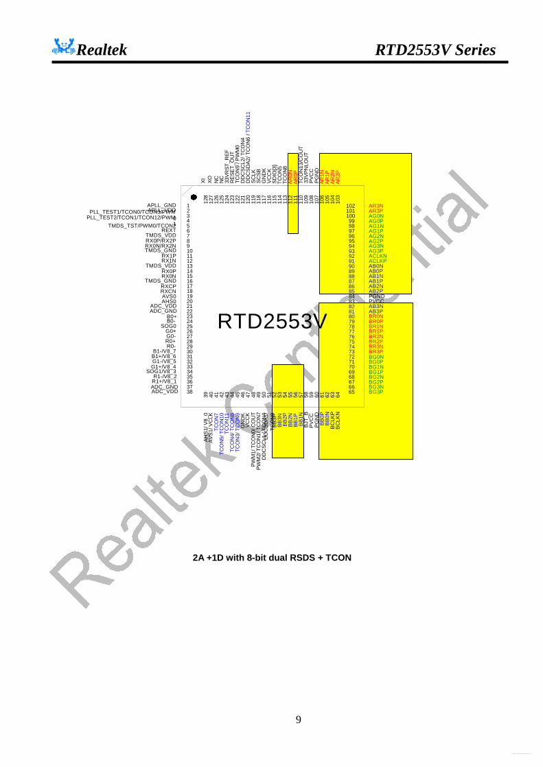
RTD2553V
5251504948474645444342414039
3837363534333231302928272625242322212019181716151413121110987654321
TXEC-
NC
NC
NCNCNC
NC
NC
NC
NC
53 54 55 56 57 58 59 60 61 62 63 64
6566676869707172737475767778798081828384858687888990919293949596979899
100101102
103
104
TXE2+
NC
TXE3+TXE3-TXEC+
TXE2-TXE1+
TXOC-TXO2+
TXE1-
PVCCPGND
TXE0+TXE0-
TXO3+TXO3-TXOC+
TXO2-
NC
105
106
107
108
109
110
111
112
113
114
115
116
117
118
119
120
121
122
123
124
125
126
127
128
SDIO
[1]/
V8_
2
BJT
_B
NCNC
SCL
K/ V
16_Y
0
SDIO
[1]/
V16
_Y4
VC
CK
GN
DK
DD
CSD
A1
DD
CSC
L1
SCL
K/ V
8_6
SCSB
/ V8_
5
ADC_VDDAHS0
AH
S1/ V
8_0/
V16
_C0
AV
S1/V
CL
KNC
TXO1+TXO1-
NCNC
TXO0+TXO0-
NC
PWM
0
CO
UT
RE
SET
_OU
T
NC
NC
NC
NC
NC
33V
PNLO
UT
VC
CK
GN
DK
DD
CSC
L2/
VC
LK
RX2P/RX0P
AVS0RXCNRXCP
TMDS_GNDRX2N/RX0N
RX0P/RX2P
TMDS_VDDRX1NRX1P
TMDS_GNDRX0N/RX2N
REXTTM D S_TST/PWM0
PLL_TEST2/PWM1
SDIO
[2]/
V8_
3SD
IO[3
]/ V
8_4
XO
B0-
ADC_GND
SOG0
R0+
R1+/ V8_1/ V16_C1
ADC_VDD
G0-G0+
B0+ADC_GND
PVC
CPG
ND
NC
NC
SD
IO[2
]/ V
16_Y
3
SDIO
[0]/
V16
_Y5
DD
CSD
A2/
V8_
7
V8_
0/ P
WM
1
B1+/ V8_6/ V16_C6G1-/ V8_5/ V16_C5
G1+/ V8_4/ V16_C4SOG1/ V8_3/ V16_C3
V16
_DE
N
V16
_HS
R1-/ V8_2/ V16_C2
R0-B1-/ V8_7/ V16_C7
TC
ON
7PLL_TEST1/PWM0
APLL_VDDAPLL_GND
NC
33V
RST
_RE
F
NC
XI
PGN
D
SCSB
/ V16
_Y1
PVC
C
SDIO
[0]/
V8_
1 S
DIO
[3]/
V16
_Y2
PWM
1/ C
OU
T/ V
16_Y
7PW
M2/
V16
_Y6
TM DS_VDDV
16_O
DD
V16
_VS
2A/Video+1D with LVDS
Optional (TMDS,
Video16, ADC port1)
http://www.DataSheet4U.net/
datasheet pdf - http://www.DataSheet4U.net/

Realtek RTD2553V Series
7
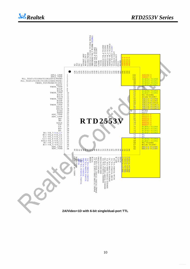
RTD2553V
5251504948474645444342414039
3837363534333231302928272625242322212019181716151413121110987654321
BG1N/ TCON0
BJT
_B
NC
BG3P/ TCON5BCLKN/ TCO N6BCLKP/ TCON 7
BB
2P/ T
CO
N11
BB
2N/ T
CO
N10
BG3N/ TCON4NC
53 54 55 56 57 58 59 60 61 62 63 64
6566676869707172737475767778798081828384858687888990919293949596979899
100101102
103
104
BR3P/ 0
BG2P/ TCON3BG2N/ TCON2BG1P/ TCON1
BR3N/ 0BR2P/ 0
AB2N/ TCON10AB1P/ TCO N9
BR2N/ 0
PV CCPG ND
BR1P/ 0BR1N/ 0
AB3P/ TCO N13AB3N/ TCON12AB2P/ TCO N11
AB1N/TCON8
AR3P/ 0
105
106
107
108
109
110
111
112
113
114
115
116
117
118
119
120
121
122
123
124
125
126
127
128
SDIO
[1]/
V8_
2/T
CO
N8
PGN
D
N CN C
PVC
C
SCL
K /
TC
ON
3 / V
16_Y
0
SDIO
[1]/
TC
ON
7/ V
16_Y
4
VC
CK
GN
DK
DD
CSD
A1/
TC
ON
9D
DC
SCL
1 / T
CO
N4
SCL
K/V
8_6/
TC
ON
3SC
SB/V
8_5/
TC
ON
7
AH S0AV S0
ADC_GND
TC
ON
11/ V
16_O
DD
AG 1N / TCON 0
ACLKP/ TCO N7ACLKN/ TCON6
AG2P/ TCO N3AG2N/ TCO N2
AG 3P/ TCON5AG 3N / TCON 4
AG 1P/ TCON1
TC
ON
9 / P
WM
0
VC
CK
RE
SET
_OU
T
AR3N/ 0
AR
2P/ 0
AR
2N/ 0
AR
1P/ 0
AR
1N/ 0
33V
PNL
OU
T
GN
DK
TC
ON
13/C
OU
T
DD
CSC
L2/
VC
LK
/TC
ON
4
TMDS_V DD
RXCNRXCP
TMD S_G NDRX0NRX 0P
TMDS_V DD
RX1NRX 1P
TMDS_G NDRX0N/RX2NRX 0P/RX 2P
REX TT M DS_TST/PWM 0/TCON 2
PLL_TEST2/TCO N1/TCO N12/PW M 1
SDIO
[2]/
V8_
3/T
CO
N5
SDIO
[3]/
V8_
4/T
CO
N9
XO
B0+
R1-/V8_2/V 16_C2
B0-
G0-
R1+/V8_1/V16_C1
ADC_VDD
G 0+SOG 0
TC
ON
5/ T
CO
N10
/ V16
_DE
N
ADC_G NDAD C_VD D
BB
3P/ T
CO
N13
BB
3N/ T
CO
N12
BB1P/ TCON 9BB1N/ TCO N8
SD
IO[2
] / T
CO
N11
/ V
16_Y
3
SDIO
[0] /
TC
ON
13 /
V16
_Y5
DD
CSD
A2
/ V8_
7 / T
CO
N6
/ TC
ON
11
V8_
0 / P
WM
1/ T
CO
N2
/ TC
ON
7
PWM
1 / T
CO
N0
/ CO
UT
/ V
16_Y
7
B1+/V8_6/V 16_C6B1-/V8_7/V 16_C7
G1+/V8_4/V 16_C4G 1-/V8_5/V 16_C5
AH
S1/ V
8_0/
V 1
6_C
0A
VS1
/ VC
LK
SOG1/V8_3/V 16_C3
R0+R0-
PWM
2 / T
CO
N1
/ TC
ON
7/ V
16_Y
6
PLL_TEST1/TCON 0/TCON3/PW M 0APLL_V DDAPLL_G ND
NC
33V
RST
_RE
F
NC
XI
PGN
D
SCSB
/ T
CO
N12
/ V
16_Y
1
PVC
C
SDIO
[0]/
V8_
1/T
CO
N10
SD
IO[3
] / T
CO
N0
/ V16
_Y2
TC
ON
4/ T
CO
N8/
V16
_HS
TC
ON
7
TC
ON
3/ T
CO
N9/
V16
_VS
2A/Video+1D with 6-bit single/dual-port RSDS + TCON
http://www.DataSheet4U.net/
datasheet pdf - http://www.DataSheet4U.net/

Realtek RTD2553V Series
8
RTD2553V
5251504948474645444342414039
3837363534333231302928272625242322212019181716151413121110987654321
BR2N/ TCO N0
BJT
_B
BG0P/ AB3PBG1N/ TCON4BG1P/ TCON5
BG3P/ TCON9BG3N/ TCON8
BG0N/ AB3N
53 54 55 56 57 58 59 60 61 62 63 64
6566676869707172737475767778798081828384858687888990919293949596979899
100101102
103
104
BR1P/ 0
BR3P/ TCON 3BR3N/ TCO N2BR2P/ TCON 1
BR1N/ 0BR0P/ 0
AB1N/ TCON10AB0P/ TCO N9
BR0N/ 0
PV CCPG ND
00
AB2P/ TCO N13AB2N/ TCON12AB1P/ TCO N11
AB0N/TCON8
AG 0P/ TCON1
105
106
107
108
109
110
111
112
113
114
115
116
117
118
119
120
121
122
123
124
125
126
127
128
AR
0P/ V
8_0/
TC
ON
2/ T
CO
N7
PGN
DPV
CC
BB
0N/ T
CO
N12
BB
2N/ S
DIO
[3]/
TC
ON
0/ V
16_Y
2
VC
CK
GN
DK
DD
CSD
A1/
TC
ON
9D
DC
SCL
1 / T
CO
N4
SCL
K/ V
8_6/
TC
ON
3SC
SB/ V
8_5/
TC
ON
7
AH S0AV S0
ADC_GND
TC
ON
11AG 1N / TCON 2
ACLKP/ TCO N7ACLKN/ TCON6
AG 2P/ 0AG 2N / 0
AG 3P/ TCON5AG 3N / TCON 4
AG 1P/ TCON3
TC
ON
9 / P
WM
0
VC
CK
RE
SET
_OU
T
AG 0N / TCON 0AR3P/ 0AR3N/ 0
AR
2P/ 0
AR
2N/ 0
33V
PNL
OU
T
GN
DK
TC
ON
13/C
OU
T
DD
CSC
L2/
VC
LK/ T
CO
N4
TMDS_V DD
RXCNRXCP
TMD S_G NDRX0NRX 0P
TMDS_V DD
RX1NRX 1P
TMDS_G NDRX0N/RX2NRX 0P/RX 2P
REX TT M DS_TST/PWM 0/TCON 2
PLL_TEST2/TCO N1/TCO N12/PW M 1
AR
0N/ S
DIO
[0]/
V8_
1/ T
CO
N10
SDIO
[3]/
V8_
4/ T
CO
N9
XO
B0+
R1-/V8_2/ V 16_C2
B0-
G0-
R1+/ V8_1/ V16_C1
ADC_VDD
G 0+SOG 0
TC
ON
5/ T
CO
N10
ADC_G NDAD C_VD D
BC
LK
P/ T
CO
N11
BC
LK
N/ T
CO
N10
BG2P/ TCON7BG2N/ TCON6
BB
1P/ S
CSB
/ TC
ON
12/ V
16_Y
1
BB
2P/ S
DIO
[2]/
TC
ON
11/ V
16_Y
3
DD
CSD
A2/
V8_
7/ T
CO
N6
/ TC
ON
11
AR
1P/ 0
BB
3P/ S
DIO
[0]/
TC
ON
13/ V
16_Y
5
B1+/ V8_6/ V 16_C6B1-/ V8_7/ V 16_C7
G1+/ V8_4/ V 16_C4G1-/V8_5/ V 16_C5
AH
S1/ V
8_0/
V16
_C0
AV
S1/ V
CLK
SOG1/V8_3/ V 16_3
R0+R0-
BB
3N/ S
DIO
[1]/
TC
ON
7/ V
16_Y
4
PLL_TEST1/TCON 0/TCON3/PW M 0APLL_V DDAPLL_G ND
NC
33V
RST
_RE
F
NC
XI
PGN
DB
B0P
/ TC
ON
13
PVC
C
AR
1N/ 0
BB
1N/ S
CL
K/ T
CO
N3/
V16
_Y0
TC
ON
4/ T
CO
N8
TC
ON
7
TC
ON
3/ T
CO
N9
SDIO
[2]/
V8_
3/ T
CO
N5
SDIO
[1]/
V8_
2/ T
CO
N8
PWM
2/ T
CO
N1/
TC
ON
7/ V
16_Y
6PW
M1/
TC
ON
0/ C
OU
T/ V
16_Y
7
2A/Video+1D with 8-bit single RSDS + TCON
http://www.DataSheet4U.net/
datasheet pdf - http://www.DataSheet4U.net/
Realtek RTD2553V Series
9
RTD2553V
5251504948474645444342414039
3837363534333231302928272625242322212019181716151413121110987654321
BR2N
BJT
_B
BG0PBG1NBG1P
BG3PBG3N
BG0N
53 54 55 56 57 58 59 60 61 62 63 64
6566676869707172737475767778798081828384858687888990919293949596979899
100101102
103
104
BR1P
BR3PBR3NBR2P
BR1NBR0P
AB1NAB0P
BR0N
PVCCPGND
AB3PAB3N
AB2PAB2NAB1P
AB0N
AG0P
105
106
107
108
109
110
111
112
113
114
115
116
117
118
119
120
121
122
123
124
125
126
127
128
AR
0P
PG
ND
PV
CC
BB
0N
BB
2N
VC
CK
GN
DK
DD
CS
DA
1/
TC
ON
9
DD
CS
CL1
/T
CO
N4
SC
LKS
CS
B
AHS0AVS0
ADC_GND
TC
ON
11AG1N
ACLKPACLKN
AG2PAG2N
AG3PAG3N
AG1PT
CO
N9
/ PW
M0
VC
CK
RE
SE
T_O
UT
AG0NAR3PAR3N
AR
2PA
R2N
33V
PN
LO
UT
GN
DK
TC
ON
13/
CO
UT
DD
CS
CL2
/ TC
ON
4
TMDS_VDD
RXCNRXCP
TMDS_GNDRX0NRX0P
TMDS_VDD
RX1NRX1P
TMDS_GNDRX0N/RX2NRX0P/RX2P
REXTTMDS_TST/PWM0/TCON2
PLL_TEST2/TCON1/TCON12/PWM1
AR
0N
SD
IO[3
]
XO
B0+
R1-/V8_2
B0-
G0-
R1+/V8_1
ADC_VDD
G0+SOG0
TC
ON
5/ T
CO
N10
ADC_GNDADC_VDD
BC
LKP
BC
LKN
BG2PBG2N
BB
1P
BB
2P
DD
CS
DA
2/ T
CO
N6
/TC
ON
11
AR
1P
BB
3P
B1+/V8_6B1-/V8_7
G1+/V8_4G1-/V8_5
AH
S1/
V8_
0A
VS
1/ V
CLK
SOG1/V8_3
R0+R0-
BB
3N
PLL_TEST1/TCON0/TCON3/PWM0
APLL_VDDAPLL_GND
NC
33V
RS
T_R
EF
NC
XI
PG
ND
BB
0P
PV
CC
AR
1N
BB
1N
TC
ON
4/ T
CO
N8
TC
ON
7
TC
ON
3/ T
CO
N9
TC
ON
5T
CO
N8
PW
M2/
TC
ON
1/ T
CO
N7
PW
M1/
TC
ON
0/ C
OU
T
2A +1D with 8-bit dual RSDS + TCON
http://www.DataSheet4U.net/
datasheet pdf - http://www.DataSheet4U.net/
Realtek RTD2553V Series
10
R T D 2553V
5251504948474645444342414039
3837363534333231302928272625242322212019181716151413121110987654321
BR E D 2/ 0
TC
ON
3/ T
CO
N9/
V16
_VS
N C
B G RN 7/ T C O N 5N C / T C O N 6B CLK/ T C O N 7
BB
LU
5/ T
CO
N11
BB
LU
4/ T
CO
N10
B G R N 6/ T C O N 4N C
53 54 55 56 57 58 59 60 61 62 63 64
6566676869707172737475767778798081828384858687888990919293949596979899
100101102
103
104
B RE D 7/ 0
BJT
_B
B G R N 5/ T CO N 3B G R N 4/ T CO N 2
B RED 3/ 0
B RE D 6/ 0B RE D 5/ 0
ABLU 4/T C O N 10ABLU 3/ T C O N 9
B RE D 4/ 0
PVCCPGND
BGRN 3/ T C O N 1B G R N 2/ T C O N 0
A B LU 7/ T C O N 13ABLU 6/ T C O N 12ABLU 5/ T C O N 11
ABLU 2/ T C O N 8
ARED 7/ 0
105
106
107
108
109
110
111
112
113
114
115
116
117
118
119
120
121
122
123
124
125
126
127
128
SDIO
[1]/
V8_
2/ T
CO
N8
PGN
D
N CN C
PVC
C
SCL
K/ T
CO
N3/
V16
_Y0
SDIO
[1]/
TC
ON
7/ D
EN
A /
V16
_Y4
VC
CK
GN
DK
DD
CSD
A1/
TC
ON
9D
DC
SCL
1/T
CO
N4
SCL
K/ V
8_6/
TC
ON
3SC
SB/ V
8_5/
TC
ON
7
AH S 0AV S 0
AD C _G N DAD C_V D D
AG R N 2/ T C O N 0
A C LK/ T CO N 7N C / T C O N 6
AG R N 5/T C O N 3AG R N 4/ T C O N 2
A G R N 7/ T C O N 5A G R N 6/ T C O N 4
A G R N 3/ T C O N 1
VC
CK
33V
PNL
OU
T
GN
DK
A R E D 6/ 0
AR
ED
5/ 0
AR
ED
4/ 0
AR
ED
3/ 0
AR
ED
2/ 0
TC
ON
9/ P
WM
0R
ESE
T_O
UT
TC
ON
13/ C
OU
T
DD
CSC
L2/
VC
LK/ T
CO
N4/
DE
NA
T M D S _V D D
RX CNRX CP
TM D S _G N DR X 0NR X 0P
T M D S _V D D
RX 1NR X 1P
T M D S _G N DRX 2NR X 2P
R E X TT M D S _T ST /PW M 0/T C O N 2
PLL_T E ST 2/T C O N 1/T C O N 12/D H S /PW M 1
SDIO
[2]/
V8_
3/ T
CO
N5
SDIO
[3]/
V8_
4/ T
CO
N9
XO
B 0+
R 1-/ V 8_2/ V 16_C 2
B0-
G 0-
R 1+/ V 8_1/ V 16_C1
TC
ON
7
G 0+SO G 0
PWM
2/ T
CO
N1/
TC
ON
7/ D
VS/
V16
_Y6
AD C _G N DAD C _V D D
BB
LU
7/ T
CO
N13
BB
LU
6/ T
CO
N12
BB LU 3/ T C O N 9B B LU 2/ T C O N 8
SD
IO[2
]/ T
CO
N11
/ DH
S/ V
16_Y
3
SDIO
[0]/
TC
ON
13/ V
16_Y
5
DD
CS
DA
2/ V
8_7/
TC
ON
6/ T
CO
N11
V8_
0/ T
CO
N2/
TC
ON
7
PWM
1/ T
CO
N0/
DH
S/ C
OU
T /V
16_Y
7
B 1+/ V 8_6/ V 16_C 6B1-/ V 8_7/ V 16_C 7
G 1+/ V 8_4/ V 16_C 4G 1-/ V 8_5/ V 16_C 5
AV
S1/V
CL
KA
HS1
/ V8_
0/ V
16_C
0
SO G 1/ V 8_3/ V 16_C 3
R 0+R0-
TC
ON
5/ T
CO
N10
/ V16
_DE
NPLL_T E S T 1/T C O N 0/T C O N 3/D V S /PW M 0
APLL_V D DAPLL_G N D
NC
33V
RST
_RE
F
NC
XI
PGN
D
SCSB
/ TC
ON
12/ V
16_Y
1
PVC
C
SDIO
[0]/
V8_
1/ T
CO
N10
SD
IO[3
]/ T
CO
N0/
V16
_Y2
TC
ON
11/ V
16_O
DD
TC
ON
4/ T
CO
N8/
V16
_HS
2A/Video+1D with 6-bit single/dual-port TTL
http://www.DataSheet4U.net/
datasheet pdf - http://www.DataSheet4U.net/

Realtek RTD2553V Series
11
RTD2553V
5251504948474645444342414039
3837363534333231302928272625242322212019181716151413121110987654321
BRED2/ 0
BJT
_B
NC
BGRN7/ TCON5BBLU0/ TCON6BBLU1/TCON7
BB
LU
5/ T
CO
N11
BB
LU
4/ T
CO
N10
BGRN6/ TCON4NC
53 54 55 56 57 58 59 60 61 62 63 64
6566676869707172737475767778798081828384858687888990919293949596979899
100101102
103
104
BGRN3/ TCON1
TC
ON
3/ T
CO
N9
BGRN5/ TCON3BGRN4/ TCON2
BRED3/ 0
BGRN2/ TCON0BRED7/ 0
ABLU4/ TCON10ABLU3/ TCON9
BRED6/ 0
PVCCPGND
BRED5/ 0BRED4/ 0
ABLU7/ TCON13ABLU6/ TCON12ABLU5/ TCON11
ABLU2/ TCON8
ARED7/ 0
105
106
107
108
109
110
111
112
113
114
115
116
117
118
119
120
121
122
123
124
125
126
127
128
AG
RN
1
PGN
D
NCNC
PVC
C
BG
RN
1
DE
NA
/ TC
ON
7
VC
CK
GN
DK
DD
CSD
A1/
TC
ON
9D
DC
SCL
1/ T
CO
N4
SCL
KSC
SB
AHS0AVS0
ADC_GNDADC_VDD
AGRN2/ TCON0
ABLU1/ TCON7ABLU0/ TCON6
AGRN5/ TCON3AGRN4/ TCON2
AGRN7/ TCON5AGRN6/ TCON4
AGRN3/ TCON1
VC
CK
33V
PNL
OU
T
GN
DK
ARED6/ 0
AR
ED
5/ 0
AR
ED
4/ 0
AR
ED
3/ 0
AR
ED
2/ 0
33V
RST
_RE
FR
ESE
T_O
UT
TC
ON
13/ C
OU
T
DD
CSC
L2/
DE
NA
/ TC
ON
4TMDS_VDD
RXCNRXCP
TMDS_GNDRX0NRX0P
TM DS_VDD
RX1NRX1P
TMDS_GNDRX2NRX2P
REXTTM DS_TST/ TCON2/ PWM0
PLL_TEST2/ DHS/ TCON1/ TCON12/ PWM1
AG
RN
0SD
IO[3
]
XO
B0+
R1-/ V8_2
B0-
G0-
R1+/ V8_1
TC
ON
7
G0+SOG0
TC
ON
5/ T
CO
N10
ADC_GNDADC_VDD
BB
LU
7/ T
CO
N13
BB
LU
6/T
CO
N12
BBLU3/ TCON9BBLU2/ TCON8
BG
RN
0
DC
LK
/ TC
ON
13
DD
CSD
A2/
DC
LK
/ TC
ON
6/ T
CO
N11
AR
ED
1
DH
S/ T
CO
N0/
PW
M1/
CO
UT
B1-/ V8_7B1+/ V8_6
G1+/ V8_4G1-/ V8_5
AH
S1/ V
8_0
AV
S1/V
CL
K
SOG1/ V8_3
R0+R0-
DV
S/ T
CO
N1/
TC
ON
7/ P
WM
2
PLL_TEST1/ DVS/ TCON0/ TCON3/ PWM0APLL_VDDAPLL_GND
NC
TC
ON
9/ P
WM
0
NCXI
PGN
D
BR
ED
0
PVC
C
AR
ED
0
BR
ED
1
TC
ON
11T
CO
N4/
TC
ON
8
2A+1D with 8-bit single/dual-port TTL
http://www.DataSheet4U.net/
datasheet pdf - http://www.DataSheet4U.net/

Realtek RTD2553V Series
12
(I/O Legend: A = Analog, I = Input, O = Output, P = Power, G = Ground) n INPUT PORT
Name I/O No Description Note ADC_GND AG 22 ADC Ground ADC_GND AG 37 ADC Ground B0+ AI 23 1st Positive BLUE analog input (Pb+) B0- AI 24 1st Negative BLUE analog input (Pb-) SOG0 AI 25 1st Sync on Green G0+ AI 26 1st Positive GREEN analog input (Y+) G0- AI 27 1st Negative GREEN analog input (Y-) R0+ AI 28 1st Positive RED analog input (Pr+) R0- AI 29 1st Negative RED analog input (Pr-) ADC_VDD AP 21 ADC Power (1.8V) ADC_VDD AP 38 ADC Power (1.8V) B1+/V8_6 AI/I 31 2nd Positive BLUE Analog input (Pb+)/
Video8_6 3.3 tolerance
B1-/V8_7 AI/I 30 2nd Positive BLUE Analog input (Pb-)/ Video8_7
3.3 tolerance
SOG1/V8_3 AI/I 34 2nd Sync on Green /Video8_3 3.3 tolerance G1+/V8_4 AI/I 33 2nd Positive GREEN analog input (Y+)/
Video8_4 3.3 tolerance
G1-/V8_5 AI/I 32 2nd Negative GREEN analog input (Y-)/ Video8_5
3.3 tolerance
R1+/V8_1 AI/I 36 2nd Positive RED analog input (Pr+)/ Video8_1
3.3 tolerance
R1-/V8_2 AI/I 35 2nd Negative RED analog input (Pr-)/ Video8_2
3.3 tolerance
AVS0 I 19 1st ADC vertical sync input Power from PIN 13
no power 5V tolerance
AHS0 I 20 1st ADC horizontal sync input Adjustable Schmidt trigger Power from PIN 13
no power 5V tolerance
AHS1/V8_0 I 39 2nd ADC horizontal sync input/Video8_0 Adjustable Schmidt trigger Power from PIN 59
no power 5V tolerance
AVS1/VCLK I 40 2nd ADC vertical sync input /Video clock Power from PIN 59
no power 5V tolerance
n PLL Name I/O Pin No Description Note
XO AO 127 Crystal OSC output XI AI 128 Reference clock input from external crystal
or from single-ended CMOS/TTL OSC 3.3V
tolerance APLL_VDD AP 2 Power for multi-phase PLL 3.3V PLL_TEST1 I/O 3 Test Pin 1
Power-on-latch for MCU crystal location
PLL_TEST2 I/O 4 Test Pin 2 M2PLL APLL_GND AG 1 Ground for multi-phase PLL
n Host interface Name I/O Pin No Description Note SDIO[0] I/O 52/112 Parallel port data [0] (Open drain)LSB 5V tolerance SDIO[1] I/O 53/113 Parallel port data [1] (Open drain) 5V tolerance
http://www.DataSheet4U.net/
datasheet pdf - http://www.DataSheet4U.net/

Realtek RTD2553V Series
13
SDIO[2] I/O 54/114 Parallel port data [2] (Open drain) 5V tolerance SDIO[3] I/O 55/115 Serial control I/F data in or Parallel port
data [3] (Open drain) MSB 5V tolerance
SCSB I 56/118 Serial control I/F chip select 5V tolerance SCLK I 57/119 Serial control I/F clock 5V tolerance n TMDS (optional)
Name I/O Pin No Description Note TMDS_TST AIO 5 TMDS_TEST Pin
Power-on-latch for host interface type
REXT AI 6 Impedance Match Reference. TMDS_VDD AP 7 TMDS power (3.3V) RX2P AI 8 Differential Data Input RX2N AI 9 Differential Data Input TMDS_GND AG 10 TMDS ground RX1P AI 11 Differential Data Input RX1N AI 12 Differential Data Input TMDS_VDD AP 13 TMDS power (3.3V) RX0P AI 14 Differential Data Input RX0N AI 15 Differential Data Input TMDS_GND AG 16 TMDS ground RXCP AI 17 Differential Data Input RXCN AI 18 Differential Data Input
n Video 8 Name I/O Pin No Description
V8_0 ~ V8_7 I 111~115, 118~120/ 39, 36~30
Video 8 data input
VCLK I 121/ 40 Video8 clock input
n Video 16 (optional) Name I/O Pin No Description
V16_Y0 ~ V16_Y7 I 57~52, 49, 48/ 39, 36~30
Video16 Y data
V16_C0 ~ V16_C0 I 39, 36~30/ 57~52, 49, 48/
Video16 C data
VCLK I 40 Video16 clock V16_DEN I 42 Video16 data enable V16_ODD I 43 Video16 ODD V16_HS I 44 Video16 HS V16_VS I 45 Video16 VS
n Pad/Digital Power & Ground
Name I/O Pin No Description Pad 3.3V Power P 59/72/83/
95/108 PVCC
Pad 3.3V Ground G 60/71/84/96/107
PGND
Digital 1.8V Power P 47/116 VCCK Digital 1.8V Ground G 46/117 GNDK
n LVDS Display Interface Name I/O No Description
http://www.DataSheet4U.net/
datasheet pdf - http://www.DataSheet4U.net/
Realtek RTD2553V Series
14
TXE3+ O 73 TXE3- O 74 TXEC+ O 75 TXEC- O 76 TXE2+ O 77 TXE2- O 78 TXE1+ O 79 TXE1- O 80 TXE0+ O 81 TXE0- O 82 TXO3+ O 85 TXO3- O 86 TXOC+ O 87 TXOC- O 88 TXO2+ O 89 TXO2- O 90 TXO1+ O 91 TXO1- O 92 TXO0+ O 93 TXO0- O 94
n 6-bit RSDS Display Interface Name I/O No Description
BB3P O 61 BB3N O 62 BB2P O 63 BB2N O 64 BB1P O 65 BB1N O 66 BCLKP O 67 BCLKN O 68 BG3P O 69 BG3N O 70 BG2P O 73 BG2N O 74 BG1P O 75 BG1N O 76 BR3P O 77 BR3N O 78 BR2P O 79 BR2N O 80 BR1P O 81 BR1N O 82 AB3P O 85 AB3N O 86 AB2P O 87 AB2N O 88 AB1P O 89 AB1N O 90 ACLKP O 91 ACLKN O 92 AG3P O 93 AG3N O 94 AG2P O 97
http://www.DataSheet4U.net/
datasheet pdf - http://www.DataSheet4U.net/
Realtek RTD2553V Series
15
AG2N O 98 AG1P O 99 AG1N O 100 AR3P O 101 AR3N O 102 AR2P O 103 AR2N O 104 AR1P O 105 AR1N O 106
n TTL 8/6 bits Interface Name I/O No Description
BBLU7 O 61 BBLU6 O 62 BBLU5 O 63 BBLU4 O 64 BBLU3 O 65 BBLU2 O 66 BBLU1/NC O 67 BBLU0/NC O 68 BGRN7 O 69 BGRN6 O 70 BGRN5 O 73 BGRN4 O 74 BGRN3 O 75 BGRN2 O 76 BGRN1/NC O 55 BGRN0/NC O 54 BRED7 O 77 BRED6 O 78 BRED5 O 79 BRED4 O 80 BRED3 O 81 BRED2 O 82 BRED1/NC O 57 BRED0/BCLK O 56 ABLU7 O 85 ABLU6 O 86 ABLU5 O 87 ABLU4 O 88 ABLU3 O 89 ABLU2 O 90 ABLU1/ACLK O 91 ABLU0/NC O 92 AGRN7 O 93 AGRN6 O 94 AGRN5 O 97 AGRN4 O 98 AGRN3 O 99 AGRN2 O 100 AGRN1/NC O 113 AGRN0/NC O 114 ARED7 O 101 ARED6 O 102
http://www.DataSheet4U.net/
datasheet pdf - http://www.DataSheet4U.net/
Realtek RTD2553V Series
16
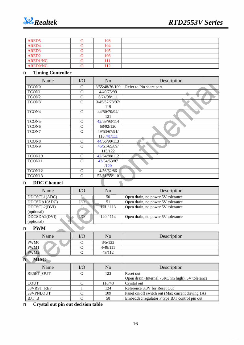
ARED5 O 103 ARED4 O 104 ARED3 O 105 ARED2 O 106 ARED1/NC O 111 ARED0/NC O 112
n Timing Controller Name I/O No Description
TCON0 O 3/55/48/76/100 Refer to Pin share part. TCON1 O 4/49/75/99 TCON2 O 5/74/98/111 TCON3 O 3/45/57/73/97/
119
TCON4 O 44/50/70/94/ 121
TCON5 O 42/69/93/114 TCON6 O 68/92/120 TCON7 O 49/53/67/91/
118 /41/111
TCON8 O 44/66/90/113 TCON9 O 45/51/65/89/
115/122
TCON10 O 42/64/88/112 TCON11 O 43/54/63/87
/120
TCON12 O 4/56/62/86 TCON13 O 52/61/85/110
n DDC Channel Name I/O No Description
DDCSCL1(ADC) I 50 Open drain, no power 5V tolerance DDCSDA1(ADC) I/O 51 Open drain, no power 5V tolerance DDCSCL2(DVI) (optional)
I 121 / 113 Open drain, no power 5V tolerance
DDCSDA2(DVI) (optional)
I/O 120 / 114 Open drain, no power 5V tolerance
n PWM Name I/O No Description
PWM0 O 3/5/122 PWM1 O 4/48/111 PWM2 O 49/112
n MISC Name I/O No Description
RESET_OUT O 123 Reset out Open drain (Internal 75KOhm high), 5V tolerance
COUT O 110/48 Crystal out 33VRST_REF I 124 Reference 3.3V for Reset Out 33VPNLOUT O 109 Panel on/off switch out (Max current driving 1A) BJT_B O 58 Embedded regulator P type BJT control pin out n Crystal out pin out decision table
http://www.DataSheet4U.net/
datasheet pdf - http://www.DataSheet4U.net/

Realtek RTD2553V Series
17
Host interface MCU location Crystal pin out
Parallel Left 110 or 48
Serial Left 110 or 48
Parallel Right 110 or 48
Serial Right 110 or 48 The COUT can be output from PIN48 or PIN110, dependent on power on latch pin 3. Power on latch pins: TMDS_TST(PIN 5) – Host interface selection (1 for parallel, 0 for serial) PLL_TEST1(PIN 3) – RTD Host Interface location & Cout selection (1 for 112-115,118/119, 110, 0 for 52-57, 48)
http://www.DataSheet4U.net/
datasheet pdf - http://www.DataSheet4U.net/
Realtek RTD2553V Series
18
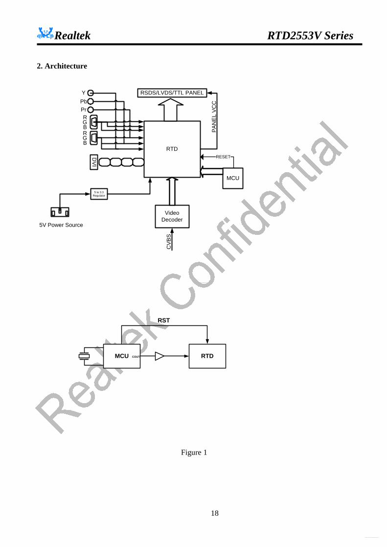
2. Architecture
RTD
Video Decoder
Y
Pb
Pr
DV
I
RGB
MCU
RSDS/LVDS/TTL PANEL
PA
NE
L V
CC
CV
BS
5 to 3.3 Regulator
5V Power Source
RGB
RESET
Figure 1
MCU RTD
RST
COUT
http://www.DataSheet4U.net/
datasheet pdf - http://www.DataSheet4U.net/
Realtek RTD2553V Series
19
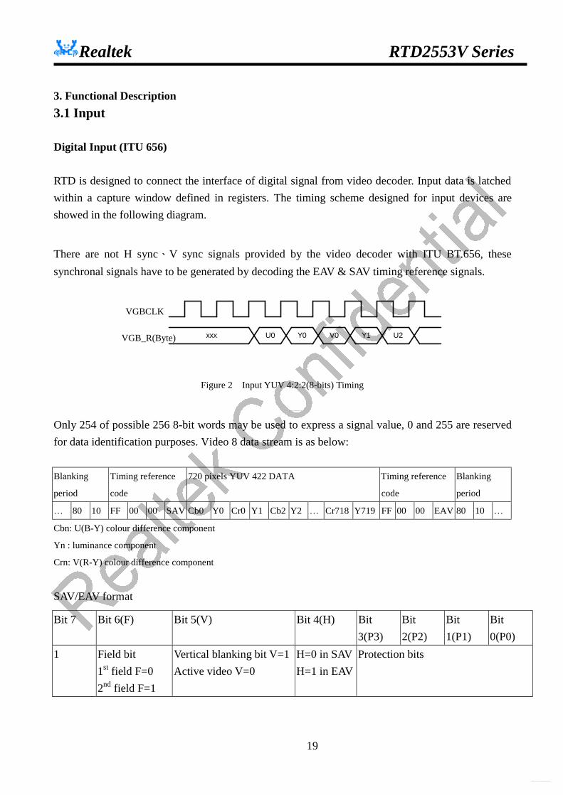
3. Functional Description 3.1 Input
Digital Input (ITU 656)
RTD is designed to connect the interface of digital signal from video decoder. Input data is latched within a capture window defined in registers. The timing scheme designed for input devices are showed in the following diagram.
There are not H sync、V sync signals provided by the video decoder with ITU BT.656, these synchronal signals have to be generated by decoding the EAV & SAV timing reference signals.
xxx U0 Y0 V0 Y1 U2
VGBCLK
VGB_R(Byte)
Figure 2 Input YUV 4:2:2(8-bits) Timing
Only 254 of possible 256 8-bit words may be used to express a signal value, 0 and 255 are reserved for data identification purposes. Video 8 data stream is as below: Blanking
period
Timing reference
code
720 pixels YUV 422 DATA Timing reference
code
Blanking
period
… 80 10 FF 00 00 SAV Cb0 Y0 Cr0 Y1 Cb2 Y2 … Cr718 Y719 FF 00 00 EAV 80 10 …
Cbn: U(B-Y) colour difference component
Yn : luminance component
Crn: V(R-Y) colour difference component
SAV/EAV format
Bit 7 Bit 6(F) Bit 5(V) Bit 4(H) Bit 3(P3)
Bit 2(P2)
Bit 1(P1)
Bit 0(P0)
1 Field bit 1st field F=0 2nd field F=1
Vertical blanking bit V=1 Active video V=0
H=0 in SAV H=1 in EAV
Protection bits
http://www.DataSheet4U.net/
datasheet pdf - http://www.DataSheet4U.net/
Realtek RTD2553V Series
20
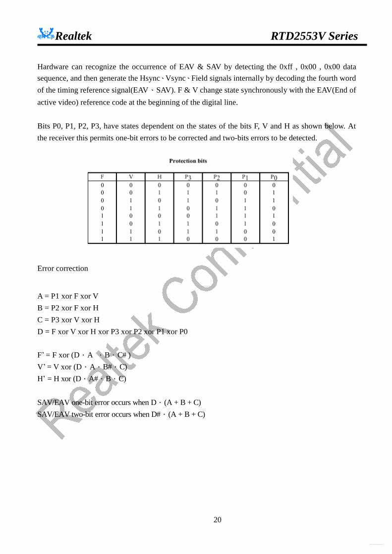
Hardware can recognize the occurrence of EAV & SAV by detecting the 0xff , 0x00 , 0x00 data sequence, and then generate the Hsync、Vsync、Field signals internally by decoding the fourth word of the timing reference signal(EAV、SAV). F & V change state synchronously with the EAV(End of active video) reference code at the beginning of the digital line. Bits P0, P1, P2, P3, have states dependent on the states of the bits F, V and H as shown below. At the receiver this permits one-bit errors to be corrected and two-bits errors to be detected.
Error correction
A = P1 xor F xor V B = P2 xor F xor H C = P3 xor V xor H D = F xor V xor H xor P3 xor P2 xor P1 xor P0 F’ = F xor (D.A .B.C# ) V’ = V xor (D.A.B#.C)
H’ = H xor (D.A#.B.C)
SAV/EAV one-bit error occurs when D.(A + B + C)
SAV/EAV two-bit error occurs when D#.(A + B + C)
http://www.DataSheet4U.net/
datasheet pdf - http://www.DataSheet4U.net/

Realtek RTD2553V Series
21
Digital Video 16-bit Input
Video 16 (CR0D[7:6] = 00) Total input 17bits(2 byte parallel data and 1 pin for clock) The red part is the timing RTD generate internally.
FF
00
00
SAV
Y0
Cb0
Y1
Cr1
FF
00
00
EAV
Y719
Cr718
ENA/Hsync
Vsync/Odd Video 16(CR0D[7:6] = 01) 與 Video16(1)類似,差在 SAV/EAV放的位置不同
00
FF
SAV
00
Y0
Cb0
Y1
Cr1
00
FF
EAV
00
Y719
Cr718
ENA/Hsync
Vsync/Odd Video 16(CR0D[7:6] = 10) ITU1120 timing.
00
00
SAV
SAV
Y0
Cb0
Y1
Cr1
FF
FF
00
00
Y719
Cr718
ENA/Hsync
Vsync/Odd
00FF
FF 00 00 EAV
EAV00
http://www.DataSheet4U.net/
datasheet pdf - http://www.DataSheet4U.net/
Realtek RTD2553V Series
22
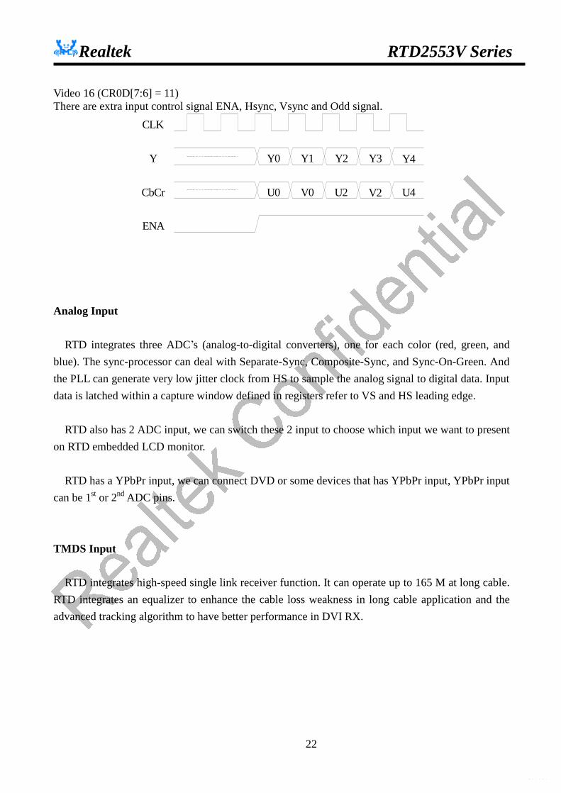
Video 16 (CR0D[7:6] = 11) There are extra input control signal ENA, Hsync, Vsync and Odd signal.
Y0 Y1 Y2 Y3 Y4
U0 V0 U2 V2 U4
CLK
Y
CbCr
ENA
Analog Input
RTD integrates three ADC’s (analog-to-digital converters), one for each color (red, green, and blue). The sync-processor can deal with Separate-Sync, Composite-Sync, and Sync-On-Green. And the PLL can generate very low jitter clock from HS to sample the analog signal to digital data. Input data is latched within a capture window defined in registers refer to VS and HS leading edge.
RTD also has 2 ADC input, we can switch these 2 input to choose which input we want to present on RTD embedded LCD monitor.
RTD has a YPbPr input, we can connect DVD or some devices that has YPbPr input, YPbPr input
can be 1st or 2nd ADC pins.
TMDS Input
RTD integrates high-speed single link receiver function. It can operate up to 165 M at long cable. RTD integrates an equalizer to enhance the cable loss weakness in long cable application and the advanced tracking algorithm to have better performance in DVI RX.
h t t p : / / w w w . D a t a S h e e t 4 U . n e t /
d a t a s h e e t p d f - h t t p : / / w w w . D a t a S h e e t 4 U . n e t /

Realtek RTD2553V Series
23
Input Capture Window
Inside RTD, there are four registers IPH_ACT_STA, IPH_ACT_WID, IPV_ACT_STA & IPV_ACT_LEN to define input capture window for the selected input video on either A or B input port while programmed analog input mode. The horizontal sync (IHS) & vertical sync (IVS) signals are used from the selected port to determine the capture window region.
IHS
Input Capture Window
IPH_ACT_STA
IPH_ACT_WID
Vertical blanking region (front porch)
Vertical blanking region (back porch)
Horizontal blankingregion (front porch)
Horizontal blankingregion (back porch)
IPV_ACT_STA
IPV_ACT_LEN
IVS
Figure 3 Input Capture Window
http://www.DataSheet4U.net/
datasheet pdf - http://www.DataSheet4U.net/

Realtek RTD2553V Series
24
3.2 Output Timing
Display Output Timing
The display output port sends single/double pixel data transfer and synchronized display timing to an external device. The display port also support display panel with 6-bit per color, turn on the dithering function to enhance color depth. In single pixel output mode, single pixel data (24-bit RGB) is transferred to display port A on each active edge of DCLK, the rate of DCLK is also equal to display pixel clock. The sync & enable signals are also sent to display port on each active edge of DCLK. In double pixel output mode, double pixel data (48-bit RGB) is transferred to display port A & B on each active edge of DCLK and the rate of DCLK is equal to half display pixel clock at this moment. The sync & enable signals are also sent to display port on each active edge of DCLK.
DCLK
DB/RGB
DEN
xxx
DA/RGB xxx rgb0 rgb1 rgb2 rgb3 rgb4 rgb5
Figure 4 TTL Single Pixel Mode Display Data Timing
DHCLK
DA/RGB
DEN
xxx rgb0 rgb2 rgb4 rgb6 rgb8 rgb10
DB/RGB xxx rgb1 rgb3 rgb5 rgb7 rgb9 rgb11
Figure 5 TTL Double Pixel Mode Display Data Timing
http://www.DataSheet4U.net/
datasheet pdf - http://www.DataSheet4U.net/
Realtek RTD2553V Series
25
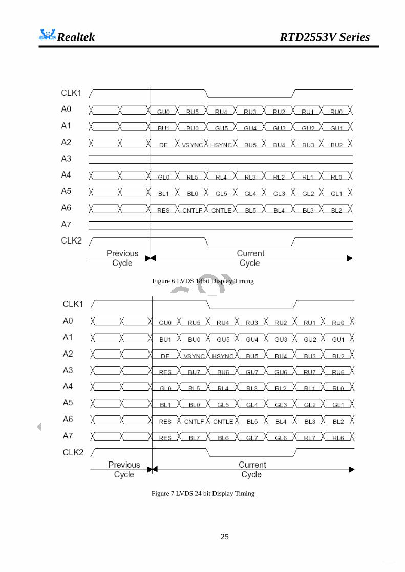
Figure 6 LVDS 18bit Display Timing
Figure 7 LVDS 24 bit Display Timing
http://www.DataSheet4U.net/
datasheet pdf - http://www.DataSheet4U.net/

Realtek RTD2553V Series
26
Figure 8 RSDS TYPE3 Display Timing
http://www.DataSheet4U.net/
datasheet pdf - http://www.DataSheet4U.net/

Realtek RTD2553V Series
27
Display Active Window
These registers define the display active window shown below in application of frame sync mode. Refer to the register description for detail.
DHS
DH_BKGD_STA
DH_ACT_STA
Vertical blanking region (front porch)
Vertical blanking region (back porch)
Horizontal blankingregion (front porch)
Horizontal blankingregion (back porch)
DV_BKGD_STA
DV_ACT_END
DEN
Display Active Window
Background Region
DVS
DH_HS_END
DH_ACT_END
DH_BKGD_END
DH_TOTAL
DV_VS_END
DV_ACT_STA
DV_BKGD_END
DV_TOTAL
Figure 9 Display Active Window Diagram
http://www.DataSheet4U.net/
datasheet pdf - http://www.DataSheet4U.net/
Realtek RTD2553V Series
28
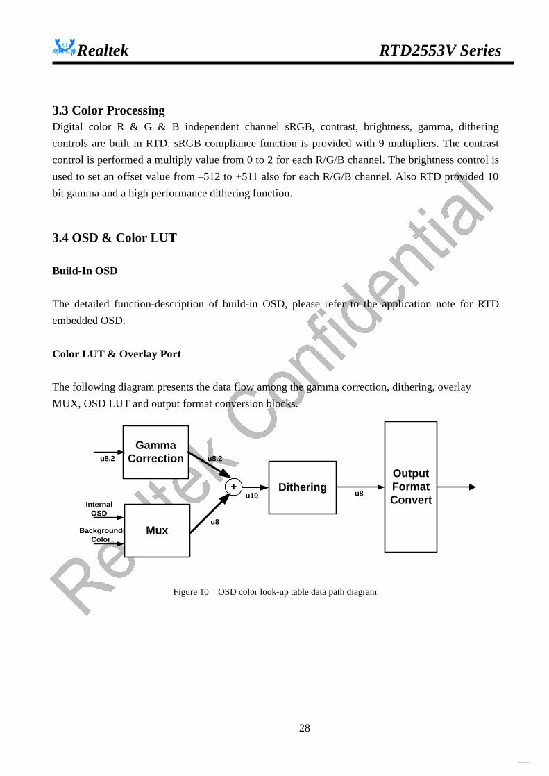
3.3 Color Processing Digital color R & G & B independent channel sRGB, contrast, brightness, gamma, dithering controls are built in RTD. sRGB compliance function is provided with 9 multipliers. The contrast control is performed a multiply value from 0 to 2 for each R/G/B channel. The brightness control is used to set an offset value from –512 to +511 also for each R/G/B channel. Also RTD provided 10 bit gamma and a high performance dithering function.
3.4 OSD & Color LUT
Build-In OSD
The detailed function-description of build-in OSD, please refer to the application note for RTD embedded OSD.
Color LUT & Overlay Port
The following diagram presents the data flow among the gamma correction, dithering, overlay MUX, OSD LUT and output format conversion blocks.
GammaCorrection
DitheringOutputFormatConvert
Mux
u8
u8.2
InternalOSD
BackgroundColor
u10+
u8.2
u8
Figure 10 OSD color look-up table data path diagram
http://www.DataSheet4U.net/
datasheet pdf - http://www.DataSheet4U.net/
Realtek RTD2553V Series
29
3.5 Auto-Adjustment There are two main independent auto-adjustment functions supported by RTD, including auto-position & auto-tracking. The operation procedure is as following;
Auto-Position
1. Define the RGB color noise margin: When the value of color channel R or G or B is greater than these noise margins, a valid pixel is found.
2. Define the threshold-pixel for vertical boundary search 3. Define the boundary window of searching for horizontal boundary search. 4. Start auto-function. 5. The result can be read from register.
Auto-Tracking
1. Setting the control-registers for the function (auto-phase, auto-balance) according to the Control-Table.
2. Define the Threshold 3. Define the boundary window of searching for tracking window. 4. Start auto-function. 5. The result can be read from register
3.6 PLL System Inside the RTD, there are four PLL systems for display clock and ADC sample clock (PLL1, PLL2, M2PLL, DPLL ).
DCLK PLL
DPLL frequency = F_IN * DPM / DPN * Divider. F_IN is input crystal frequency. DPM and DPN is in DPLL_M and DPLL_N. Divider is in
DPLL_N, and it divide PLL frequency by 1, 2, 4 or 8. According to parameter DPN, you must set LPF Mode in DPLL_WD. If LPF Mode is 1, the
charge pump current, Ich, must be DPM/17.6, while Ich must be DPM/1.67 if LPF Mode is 0. The charge pump current Ich is in DPLL_CRNT.
Spread-Spectrum function is also build in DCLK to reduce EMI. You can control the SSP_I, SSP_W, and FMDIV to fine-tune the EMI.
http://www.DataSheet4U.net/
datasheet pdf - http://www.DataSheet4U.net/
Realtek RTD2553V Series
30
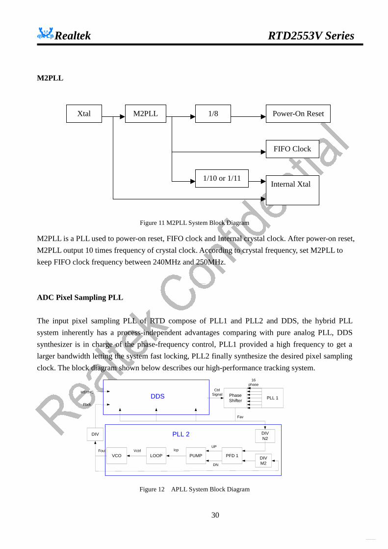
M2PLL
Figure 11 M2PLL System Block Diagram
M2PLL is a PLL used to power-on reset, FIFO clock and Internal crystal clock. After power-on reset, M2PLL output 10 times frequency of crystal clock. According to crystal frequency, set M2PLL to keep FIFO clock frequency between 240MHz and 250MHz.
ADC Pixel Sampling PLL
The input pixel sampling PLL of RTD compose of PLL1 and PLL2 and DDS, the hybrid PLL system inherently has a process-independent advantages comparing with pure analog PLL, DDS synthesizer is in charge of the phase-frequency control, PLL1 provided a high frequency to get a larger bandwidth letting the system fast locking, PLL2 finally synthesize the desired pixel sampling clock. The block diagram shown below describes our high-performance tracking system.
Figure 12 APLL System Block Diagram
PhaseShifter PLL 1
DIV
PFD 1PUMPLOOPVCO
DIVN2
DIVM2
HSYNC
Fbck
CtrlSignal
16phase
Fav
UP
DN
IcpVctrlFout
PLL 2
DDS
Xtal M2PLL 1/8 Power-On Reset
FIFO Clock
1/10 or 1/11 Internal Xtal
http://www.DataSheet4U.net/
datasheet pdf - http://www.DataSheet4U.net/
Realtek RTD2553V Series
31
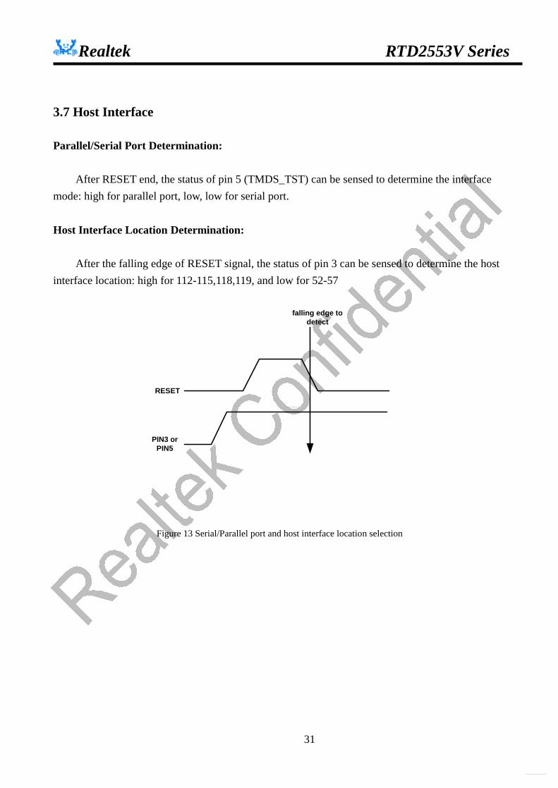
3.7 Host Interface
Parallel/Serial Port Determination:
After RESET end, the status of pin 5 (TMDS_TST) can be sensed to determine the interface mode: high for parallel port, low, low for serial port.
Host Interface Location Determination:
After the falling edge of RESET signal, the status of pin 3 can be sensed to determine the host interface location: high for 112-115,118,119, and low for 52-57
RESET
PIN3 orPIN5
falling edge todetect
Figure 13 Serial/Parallel port and host interface location selection
http://www.DataSheet4U.net/
datasheet pdf - http://www.DataSheet4U.net/

Realtek RTD2553V Series
32
Double Data Rate Serial/Parallel Interface:
Any transaction should start from asserted the SCSB low and stop after the SCSB goes high.
100n
D0[4:0]
D0[8:5]
D1[4:0]
D1[8:5]
SCSB
SCLK
SDIOX
ADRH R/WINCADRL
ADRL INC/RW D0[4:0] D0[8:5] D1[4:0] D1[8:5]
SCSB
SCLK
ADRH
Figure 14 Parallel Port Read (Upper)/Write (Below) with Dual edge data latch
SDIO0 ADRL [A0] ADRH[A4] R/W D0[0] D0[4] D1[0] D1[4] SDIO1 ADRL [A1] ADRH[A5] INC D0[1] D0[5] D1[1] D1[5] SDIO2 ADRL [A2] ADRH[A6] X D0[2] D0[6] D1[2] D1[6] SDIO3 ADRL [A3] ADRH[A7] X D0[3] D0[7] D1[3] D1[7]
Parallel port data alignment
A1
SCSB
SCLK
A2
A0
A3
A4
A5
A6
A7
RW
INC
D0
D1
D2
D3
D4
D5
D6
D7
A1
SCSB
SCLK
A2
A0
A3
A4
A5
A6
A7
RW
INC
D0
D1
D2
D3
D4
D5
D6
D7
A0 A1 A2 A3 A4 A5 A6 A7 R/W INC D0 D1 D2 D3 D4 D5 D6 D7 Serial Port Read (Upper)/Write (Below) with Dual edge data latch, and Serial port data alignment
http://www.DataSheet4U.net/
datasheet pdf - http://www.DataSheet4U.net/

Realtek RTD2553V Series
33
3.8 Reset Output We have the RESET_OUT function, and also reserve the RESET_IN function. By the bounding
of internal pins we can select two kinds of reset function. First of all is only reset-out, we can output the reset signal to MCU, and the MCU can reset the RTD by firmware. The second is RTD output reset and also reset itself. Notice that the reset output is positive polarity, besides, the reset output is open-drain pin, please don’t forget to attach a pull-up resistor (10K).
The reset function for 3.3V operating voltage detection is determined by 33VRST_REF voltage,
No matter 5V or 3.3V MCU is been used, divider the input voltage on 33VRST_REF to 2.2V for internal power sensing circuit detecting, the divider resistor should be 10K level avoiding current leakage.
Figure 15 Three kinds of RESET function
For the reset-out function, the characteristics are below:
Parameter Symbol Min. Typ. Max. Unit Detection Voltage -Vdet 1.8 2.4 V Release Voltage +Vdet - 2.6 - V
Delay Time td 50 - - ms
Reset in
RESETB
Reset out
Package
Die
http://www.DataSheet4U.net/
datasheet pdf - http://www.DataSheet4U.net/
Realtek RTD2553V Series
34
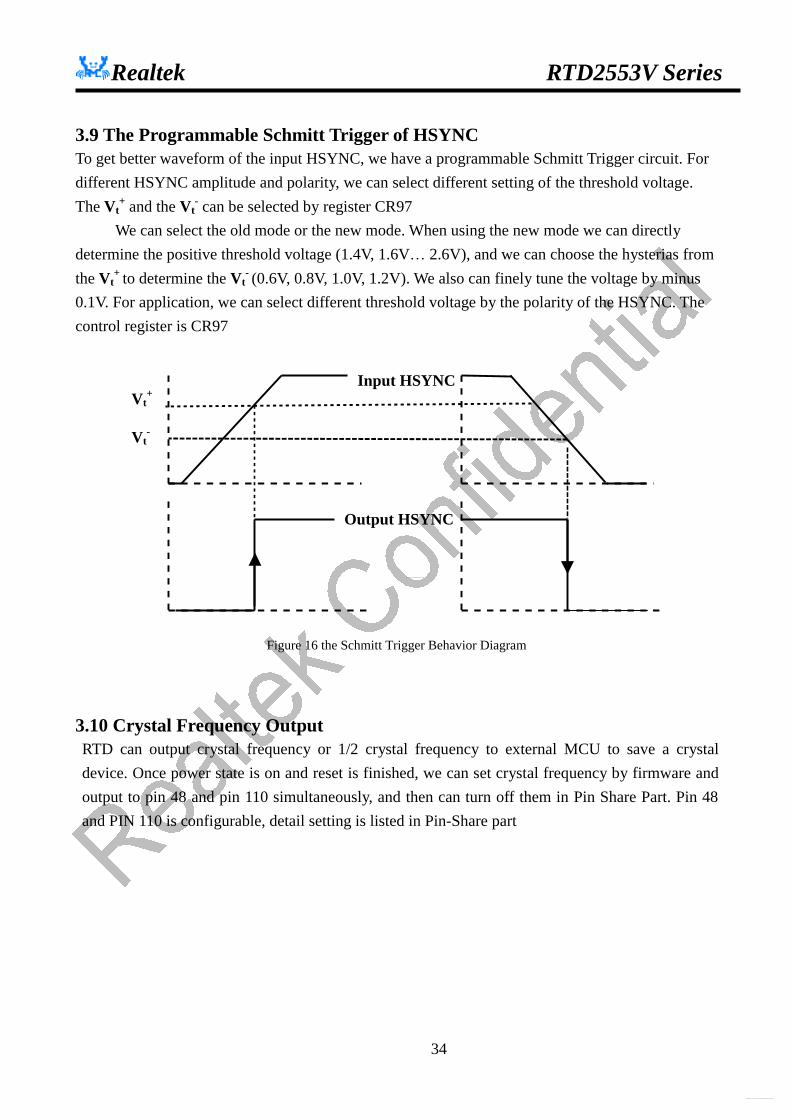
3.9 The Programmable Schmitt Trigger of HSYNC To get better waveform of the input HSYNC, we have a programmable Schmitt Trigger circuit. For different HSYNC amplitude and polarity, we can select different setting of the threshold voltage. The Vt
+ and the Vt- can be selected by register CR97
We can select the old mode or the new mode. When using the new mode we can directly determine the positive threshold voltage (1.4V, 1.6V… 2.6V), and we can choose the hysterias from the Vt
+ to determine the Vt- (0.6V, 0.8V, 1.0V, 1.2V). We also can finely tune the voltage by minus
0.1V. For application, we can select different threshold voltage by the polarity of the HSYNC. The control register is CR97
Figure 16 the Schmitt Trigger Behavior Diagram
3.10 Crystal Frequency Output RTD can output crystal frequency or 1/2 crystal frequency to external MCU to save a crystal device. Once power state is on and reset is finished, we can set crystal frequency by firmware and output to pin 48 and pin 110 simultaneously, and then can turn off them in Pin Share Part. Pin 48 and PIN 110 is configurable, detail setting is listed in Pin-Share part
Vt-
Vt+
Input HSYNC
Output HSYNC
http://www.DataSheet4U.net/
datasheet pdf - http://www.DataSheet4U.net/

Realtek RTD2553V Series
35
4. Register description Global event flag Reading unimplemented registers will return 0. Address: 00 ID_REG Default: A1h
Bit Mode Function
7:0 R MSB 4 bits: 1010 product code
LSB 4 bits: 0001 rev. code
Address: 01 HOSTCTRL Default: 02h
Bit Mode Function
7 R Display Support
0: up to SXGA
1: up to UXGA
6:3 R/W Reserved to 0
2 R/W Power Down Mode Enable
0: Normal (Default)
1: Enable power down mode
Turn off ADC R/G/B/Banggap/DPLL/LVDS/PLL1/PLL2/SOG/SYNC PROC/TMDS
1 R/W Power Saving Mode Enable
0: Normal
1: Enable power saving mode (Default)
Turn off ADC R/G/B/DPLL/LVDS/PLL1/PLL2
0 R/W Software Reset Whole Chip (Low pulse at least 8ms)
0: Normal (Default)
1: Reset
(All registers are reset to default except HOST_CTRL & M2PLL & COUT Frequency
(TCON00[3]), the only difference with Hardware-Reset is power on latch won’t work)
Address: 02 STATUS0 (Status0 Register) Default: 00h
Bit Mode Function
7 R ADC_PLL Non-Lock:
If the ADC_PLL non-lock occurs, this bit is set to “1”.
6 R Input VSYNC Error
If the input vertical sync occurs within the programmed active period, this bit is set to “1”.
5 R Input HSYNC Error
If the input horizontal sync occurs within the programmed active period, this bit is set to “1”.
4 R Input ODD Toggle Occur (For internal field odd toggle, refer to CR0F[5])
If the ODD signal (From SAV/EAV or V16_ODD) toggle occurs, this bit is set to “1”.
http://www.DataSheet4U.net/
datasheet pdf - http://www.DataSheet4U.net/
Realtek RTD2553V Series
36
3 R Video8/16 Input Vertical/Horizontal Sync Occurs
If the YUV input V or H sync edge occurs, this bit is set to “1”.
2 R ADC Input Vertical/Horizontal Sync Occurs
Input V or H sync edge occurs; this bit is set to “1”.
This mechanism refers to current selected ADC,(i.e.: we can choose from ADC0/ADC1)
1 R Input Overflow Status (Frame Sync Mode)
If an overflow in the input data capture buffer occurs, this bit is set to “1”.1
0 R Line Buffer Underflow status (Frame Sync Mode)
If an underflow in the line-buffer occurs, this bit is set to “1”.
Write to clear status.
Address: 03 STATUS1 (Status1 Register) Default: 00h
Bit Mode Function
7 R Line Buffer Overflow Status2
1: Line Buffer overflow has occurred since the last status cleared
6 R Line Buffer Underflow Status
1: Line Buffer underflow has occurred since the last status cleared
5 R DENA Stop Event Status
1: If the DENA stop event occurred since the last status cleared
4 R DENA Start Event Status
1: If the DENA start event occurred since the last status cleared
3 R DVS Start Event Status
1: If the DVS start event occurred since the last status cleared
2 R IENA Stop Event Status
1: If the IENA stop event occurred since the last status cleared
1 R IENA Start Event Status
1: If the IENA start event occurred since the last status cleared
0 R IVS Start Event Status
1: If the IVS start event occurred since the last status cleared
Write to clear status.
Address: 04 IRQ_CTRL0 (IRQ Control Register 0) Default: 00h
Bit Mode Function
7 R/W Internal IRQ Enable: (Global)
0: Disable these interrupt.
1 Only the first event of input overflow/underflow will be recorded at the same time. 2 Both input overflow/underflow status will be recorded whenever it happens.
http://www.DataSheet4U.net/
datasheet pdf - http://www.DataSheet4U.net/

Realtek RTD2553V Series
37
1: Enable these interrupt. The IRQ event of CRF9 & CR04 will be logically “OR” together.
6 R/W IRQ (ADC_PLL Non-Lock)
0: Disable the ADC_PLL non-lock error event as an interrupt source
1: Enable the ADC_PLL non-lock error event as an interrupt source
5 R/W IRQ (Input VSYNC/HSYNC Error) (DEN across Vsync or Hsync)
0: Disable the Input VSYNC/HSYNC error event as an interrupt source
1: Enable the Input VSYNC/HSYNC error event as an interrupt source
4 R/W IRQ (Input ODD Toggle Occur) (EAV/SAV from Video8/16 or V16_ODD)
0: Disable the Input ODD toggle event as an interrupt source
1: Enable the Input ODD toggle event as an interrupt source
3 R/W IRQ (Video8/16 Input Hsync/Vertical Sync Occurs)
0: Disable the Video8/16 Input Hsync or Vsync event as an interrupt source
1: Enable the Video8/16 Input Hsync or Vsync event as an interrupt source
2 R/W IRQ (ADC Input Hsync/Vertical Sync Occurs)
0: Disable the ADC Input Hsync or Vsync event as an interrupt source
1: Enable the ADC Input Hsync or Vsync event as an interrupt source
1 R/W IRQ (Line Buffer Underflow/Overflow Status)
0: Disable the Line Buffer underflow/overflow event as an interrupt source
1: Enable the Line Buffer underflow/overflow event as an interrupt source
0 -- Reserved to 0
http://www.DataSheet4U.net/
datasheet pdf - http://www.DataSheet4U.net/
Realtek RTD2553V Series
38
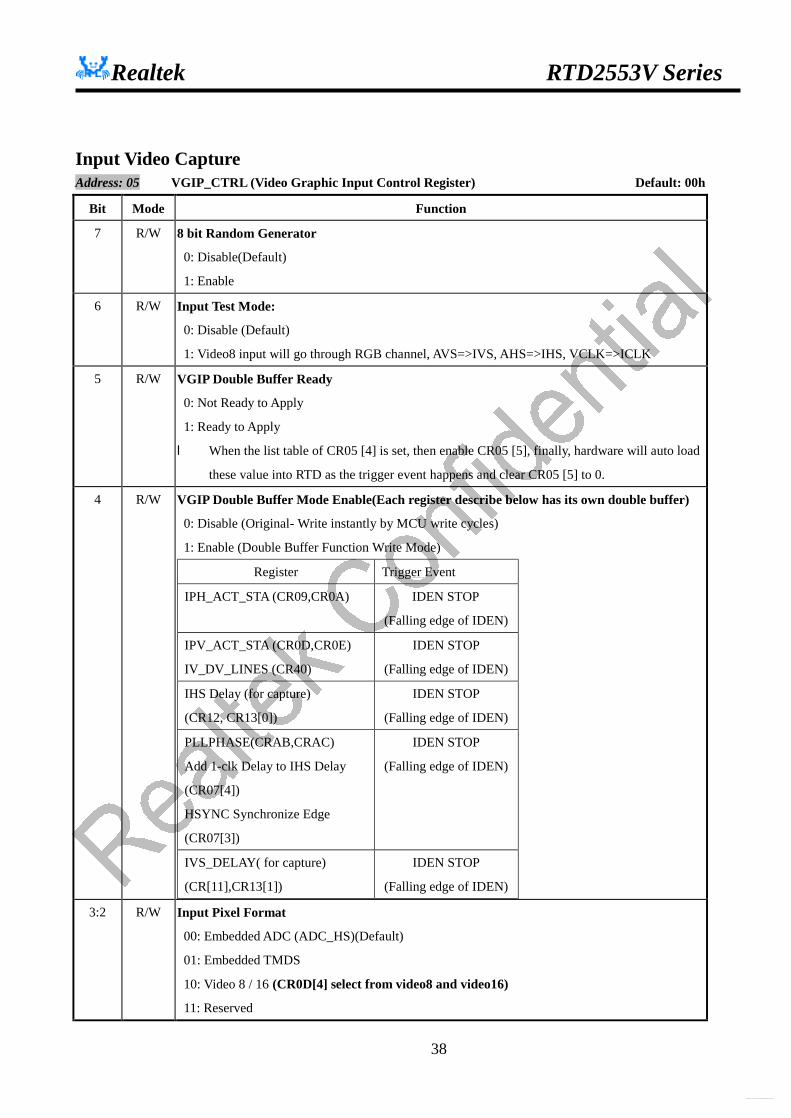
Input Video Capture Address: 05 VGIP_CTRL (Video Graphic Input Control Register) Default: 00h
Bit Mode Function
7 R/W 8 bit Random Generator
0: Disable(Default)
1: Enable
6 R/W Input Test Mode:
0: Disable (Default)
1: Video8 input will go through RGB channel, AVS=>IVS, AHS=>IHS, VCLK=>ICLK 5 R/W VGIP Double Buffer Ready
0: Not Ready to Apply
1: Ready to Apply
l When the list table of CR05 [4] is set, then enable CR05 [5], finally, hardware will auto load
these value into RTD as the trigger event happens and clear CR05 [5] to 0.
4 R/W VGIP Double Buffer Mode Enable(Each register describe below has its own double buffer)
0: Disable (Original- Write instantly by MCU write cycles)
1: Enable (Double Buffer Function Write Mode)
Register Trigger Event
IPH_ACT_STA (CR09,CR0A) IDEN STOP
(Falling edge of IDEN)
IPV_ACT_STA (CR0D,CR0E)
IV_DV_LINES (CR40)
IDEN STOP
(Falling edge of IDEN)
IHS Delay (for capture)
(CR12, CR13[0])
IDEN STOP
(Falling edge of IDEN)
PLLPHASE(CRAB,CRAC)
Add 1-clk Delay to IHS Delay
(CR07[4])
HSYNC Synchronize Edge
(CR07[3])
IDEN STOP
(Falling edge of IDEN)
IVS_DELAY( for capture)
(CR[11],CR13[1])
IDEN STOP
(Falling edge of IDEN) 3:2 R/W Input Pixel Format
00: Embedded ADC (ADC_HS)(Default)
01: Embedded TMDS
10: Video 8 / 16 (CR0D[4] select from video8 and video16)
11: Reserved
http://www.DataSheet4U.net/
datasheet pdf - http://www.DataSheet4U.net/
Realtek RTD2553V Series
39
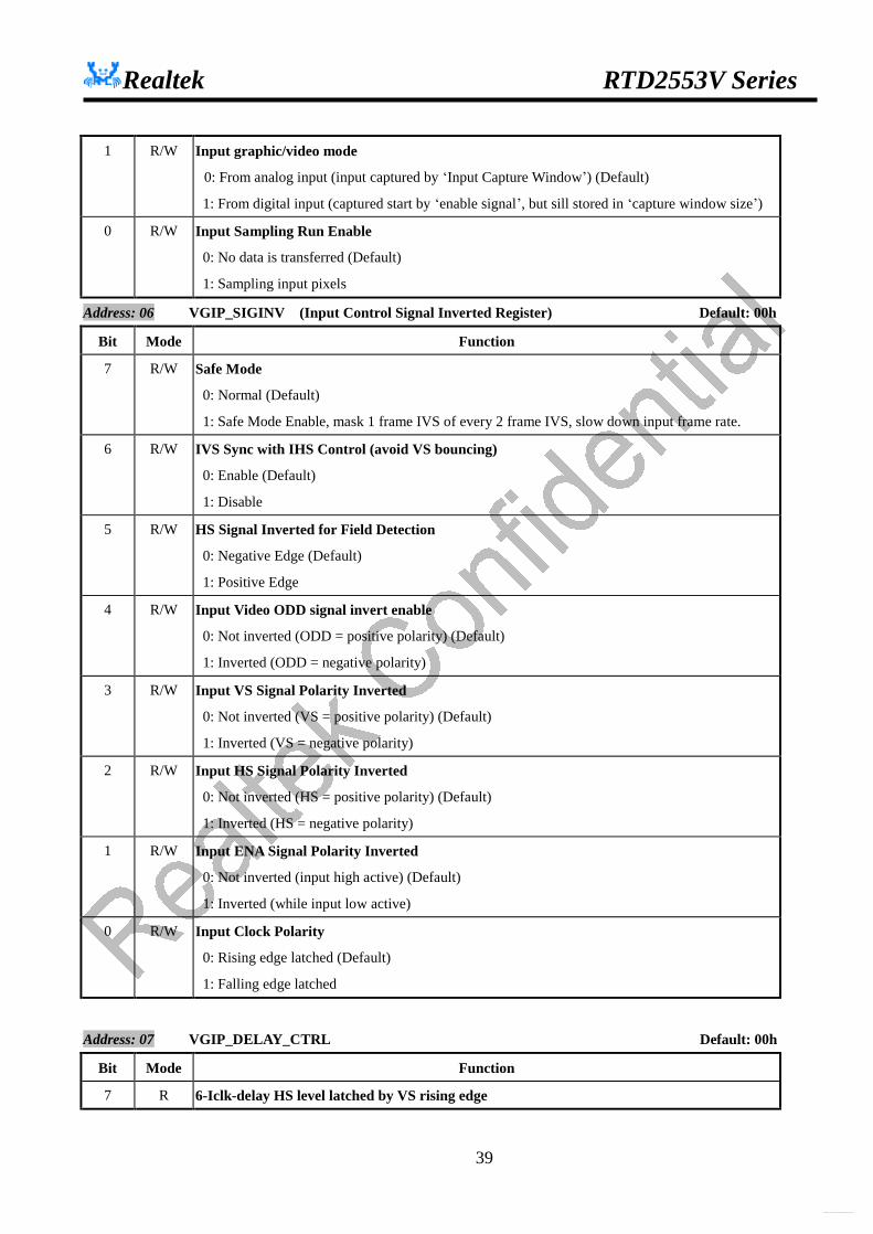
1 R/W Input graphic/video mode
0: From analog input (input captured by ‘Input Capture Window’) (Default)
1: From digital input (captured start by ‘enable signal’, but sill stored in ‘capture window size’) 0 R/W Input Sampling Run Enable
0: No data is transferred (Default)
1: Sampling input pixels
Address: 06 VGIP_SIGINV (Input Control Signal Inverted Register) Default: 00h
Bit Mode Function
7 R/W Safe Mode
0: Normal (Default)
1: Safe Mode Enable, mask 1 frame IVS of every 2 frame IVS, slow down input frame rate.
6 R/W IVS Sync with IHS Control (avoid VS bouncing)
0: Enable (Default)
1: Disable
5 R/W HS Signal Inverted for Field Detection
0: Negative Edge (Default)
1: Positive Edge
4 R/W Input Video ODD signal invert enable
0: Not inverted (ODD = positive polarity) (Default)
1: Inverted (ODD = negative polarity)
3 R/W Input VS Signal Polarity Inverted
0: Not inverted (VS = positive polarity) (Default)
1: Inverted (VS = negative polarity)
2 R/W Input HS Signal Polarity Inverted
0: Not inverted (HS = positive polarity) (Default)
1: Inverted (HS = negative polarity)
1 R/W Input ENA Signal Polarity Inverted
0: Not inverted (input high active) (Default)
1: Inverted (while input low active)
0 R/W Input Clock Polarity
0: Rising edge latched (Default)
1: Falling edge latched
Address: 07 VGIP_DELAY_CTRL Default: 00h
Bit Mode Function
7 R 6-Iclk-delay HS level latched by VS rising edge
http://www.DataSheet4U.net/
datasheet pdf - http://www.DataSheet4U.net/

Realtek RTD2553V Series
40
6 R HS level latched by VS rising edge
5 R HS level latched by 6-Iclk-delay VS rising edge
4 R/W Add one clock delay to IHS delay
0: Disable (Default)
1: Enable
3 R/W HSYNC Synchronize Edge
0: HSYNC is synchronized by the positive edge of the input clock
1: HSYNC is synchronized by the negative edge of the input clock
( HSYNC source is selected by CR48[0] and then synchronized )
2 R/W VSYNC Synchronize Edge
0: latch VS by the negative edge of input HSYNC(Default)
1: latch VS by the positive edge of input HSYNC
1:0 R/W Input Clock Delay Control:
00: Normal (Default)
01: 1ns delay
10: 2ns delay
11: 3ns delay
Address: 08 VGIP_ODD_CTRL (Video Graphic Input ODD Control Register) Default: 00h
Bit Mode Function
7 R/W ODD invert for ODD-Controlled-IVS_delay.
0: Not Invert (Default)
1: Invert
6 R/W ODD-Controlled-IVS delay one line Enable
0: Disable (Default)
1: Enable
l For both Auto and Capture
5 R/W Safe Mode ODD inversion
0: Not inverted (Default)
1: Inverted
4 R/W Force ODD toggle enable (Without ODD/EVEN toggle select in Safe Mode)
0: Disable (Default)
1: Enable
3 R/W Video 4:2:2->4:4:4 enable before Scale Down (Duplicate)
0: Disable (Default)
1: Enable
i.e. This bit should be always enable when in Video8 / 16 mode.
http://www.DataSheet4U.net/
datasheet pdf - http://www.DataSheet4U.net/

Realtek RTD2553V Series
41
2 R/W Decode Video8 or Video16 when ADC or TMDS active (CR0D[4] select from video8 and
video16)
0: Disable (Default)
1: Enable
1 R/W EAV Error Correction Enable in Video8/16
0: Disable
1: Enable
0 R/W Internal ODD signal selection
0: ODD signal from EAV or YPbPr (Default)
1: Internal Field Detection ODD signal (Also support under VGA, DVI input)
http://www.DataSheet4U.net/
datasheet pdf - http://www.DataSheet4U.net/
Realtek RTD2553V Series
42
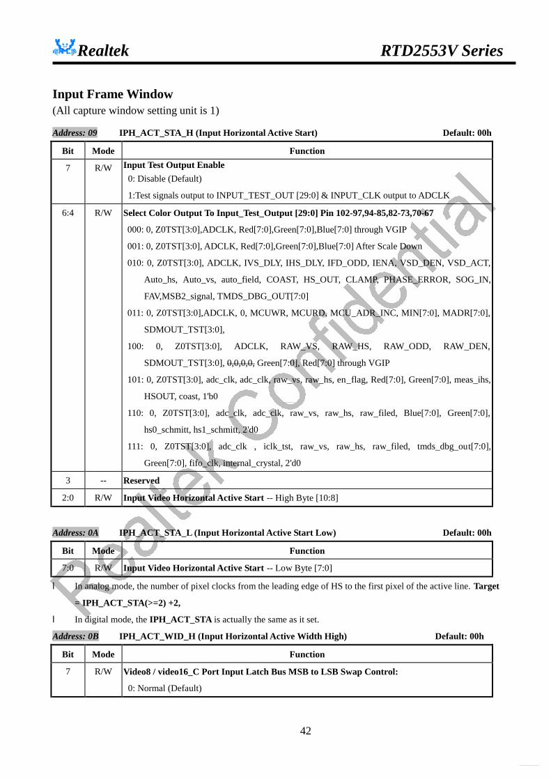
Input Frame Window (All capture window setting unit is 1)
Address: 09 IPH_ACT_STA_H (Input Horizontal Active Start) Default: 00h
Bit Mode Function
7 R/W Input Test Output Enable 0: Disable (Default)
1:Test signals output to INPUT_TEST_OUT [29:0] & INPUT_CLK output to ADCLK
6:4 R/W Select Color Output To Input_Test_Output [29:0] Pin 102-97,94-85,82-73,70-67
000: 0, Z0TST[3:0],ADCLK, Red[7:0],Green[7:0],Blue[7:0] through VGIP 001: 0, Z0TST[3:0], ADCLK, Red[7:0],Green[7:0],Blue[7:0] After Scale Down
010: 0, Z0TST[3:0], ADCLK, IVS_DLY, IHS_DLY, IFD_ODD, IENA, VSD_DEN, VSD_ACT,
Auto_hs, Auto_vs, auto_field, COAST, HS_OUT, CLAMP, PHASE_ERROR, SOG_IN,
FAV,MSB2_signal, TMDS_DBG_OUT[7:0]
011: 0, Z0TST[3:0],ADCLK, 0, MCUWR, MCURD, MCU_ADR_INC, MIN[7:0], MADR[7:0],
SDMOUT_TST[3:0],
100: 0, Z0TST[3:0], ADCLK, RAW_VS, RAW_HS, RAW_ODD, RAW_DEN,
SDMOUT_TST[3:0], 0,0,0,0, Green[7:0], Red[7:0] through VGIP
101: 0, Z0TST[3:0], adc_clk, adc_clk, raw_vs, raw_hs, en_flag, Red[7:0], Green[7:0], meas_ihs,
HSOUT, coast, 1'b0
110: 0, Z0TST[3:0], adc_clk, adc_clk, raw_vs, raw_hs, raw_filed, Blue[7:0], Green[7:0],
hs0_schmitt, hs1_schmitt, 2'd0
111: 0, Z0TST[3:0], adc_clk , iclk_tst, raw_vs, raw_hs, raw_filed, tmds_dbg_out[7:0],
Green[7:0], fifo_clk, internal_crystal, 2'd0
3 -- Reserved
2:0 R/W Input Video Horizontal Active Start -- High Byte [10:8]
Address: 0A IPH_ACT_STA_L (Input Horizontal Active Start Low) Default: 00h
Bit Mode Function
7:0 R/W Input Video Horizontal Active Start -- Low Byte [7:0]
l In analog mode, the number of pixel clocks from the leading edge of HS to the first pixel of the active line. Target
= IPH_ACT_STA(>=2) +2,
l In digital mode, the IPH_ACT_STA is actually the same as it set.
Address: 0B IPH_ACT_WID_H (Input Horizontal Active Width High) Default: 00h
Bit Mode Function
7 R/W Video8 / video16_C Port Input Latch Bus MSB to LSB Swap Control:
0: Normal (Default)
http://www.DataSheet4U.net/
datasheet pdf - http://www.DataSheet4U.net/

Realtek RTD2553V Series
43
1: Switched Video8 / video16_C port MSB to LSB sequence into LSB to MSB
6 R/W ADC input G/B Swap
0: No Swap
1: Swap
5 R/W ADC input R/B Swap
0: No Swap
1: Swap
4 R/W ADC input R/G Swap
0: No Swap
1: Swap
3 R/W Double Clock Input
0: Single Clock
1: Double Clock
this bit should be set double clock when using video 8 input
2:0 R/W Input Video Horizontal Active Width – High Byte [10:8]
B
G
R R
G
B
CR0B[4] CR0B[5] CR0B[6]
RTD Address: 0C IPH_ACT_WID_L (Input Horizontal Active Width Low) Default: 00h
Bit Mode Function
7:0 R/W Input Video Horizontal Active Width -- Low Byte [7:0]
This register defines the number of active pixel clocks to be captured.
Address: 0D IPV_ACT_STA_H (Input Vertical Active Start High) Default: 00h
Bit Mode Function
7:6 R/W Video16 mode (reference to Digital Video 16-bit Input)
5 R/W Video16_Y / Video16_C swap
0: disable
1: enable 4 R/W Video8 / Video16 select
0: video8
1: video16 3 R/W Video16_Y Port Input Latch Bus MSB to LSB Control:
0: Normal (Default)
1: Switched video16_Y port MSB to LSB sequence into LSB to MSB
http://www.DataSheet4U.net/
datasheet pdf - http://www.DataSheet4U.net/
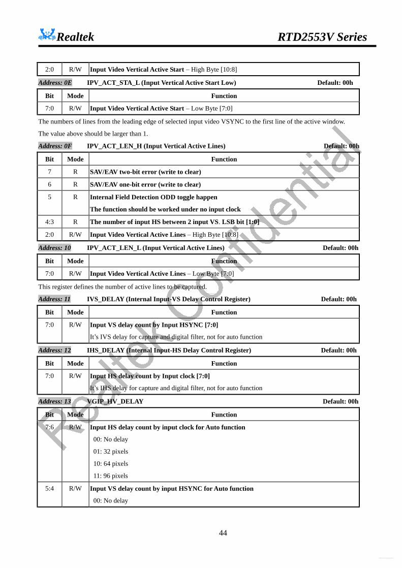
Realtek RTD2553V Series
44
2:0 R/W Input Video Vertical Active Start – High Byte [10:8]
Address: 0E IPV_ACT_STA_L (Input Vertical Active Start Low) Default: 00h
Bit Mode Function
7:0 R/W Input Video Vertical Active Start – Low Byte [7:0]
The numbers of lines from the leading edge of selected input video VSYNC to the first line of the active window.
The value above should be larger than 1.
Address: 0F IPV_ACT_LEN_H (Input Vertical Active Lines) Default: 00h
Bit Mode Function
7 R SAV/EAV two-bit error (write to clear)
6 R SAV/EAV one-bit error (write to clear)
5 R Internal Field Detection ODD toggle happen
The function should be worked under no input clock
4:3 R The number of input HS between 2 input VS. LSB bit [1:0]
2:0 R/W Input Video Vertical Active Lines – High Byte [10:8]
Address: 10 IPV_ACT_LEN_L (Input Vertical Active Lines) Default: 00h
Bit Mode Function
7:0 R/W Input Video Vertical Active Lines – Low Byte [7:0]
This register defines the number of active lines to be captured.
Address: 11 IVS_DELAY (Internal Input-VS Delay Control Register) Default: 00h
Bit Mode Function
7:0 R/W Input VS delay count by Input HSYNC [7:0]
It’s IVS delay for capture and digital filter, not for auto function
Address: 12 IHS_DELAY (Internal Input-HS Delay Control Register) Default: 00h
Bit Mode Function
7:0 R/W Input HS delay count by Input clock [7:0]
It’s IHS delay for capture and digital filter, not for auto function
Address: 13 VGIP_HV_DELAY Default: 00h
Bit Mode Function
7:6 R/W Input HS delay count by input clock for Auto function
00: No delay
01: 32 pixels
10: 64 pixels
11: 96 pixels
5:4 R/W Input VS delay count by input HSYNC for Auto function
00: No delay
http://www.DataSheet4U.net/
datasheet pdf - http://www.DataSheet4U.net/
Realtek RTD2553V Series
45
01: 3 line
10: 7 line
11: 15 line
3:2 -- Reserved to 0
1 R/W Input VS delay count by Input HSYNC[8]
0 R/W Input HS delay count by Input clock[8]
FIFO Window Address: 14 DRL_H_BSU (Display Read High Byte Before Scaling-Up) Default: 00h
Bit Mode Function
7 -- Reserved
6:4 R/W Display window read width before scaling up: High Byte [10:8]
3 -- Reserved
2:0 R/W Display window read length before scaling up: High Byte [10:8]
Address: 15 DRW_L_BSU (Display Read Width Low Byte Before Scaling-Up) Default: 00h
Bit Mode Function
7:0 R/W Display window read width before scaling up: Low Byte [7:0]
Address: 16 DRL_L_BSU (Display Read Length Low Byte Before Scaling-Up) Default: 00h
Bit Mode Function
7:0 R/W Display window read length before scaling up: Low Byte [7:0]
l The setting above should be use 2 as unit
IHS_DELAYCR13[0] / CR12
IHS_DELAY FORAUTO
CR13[7:6]
1 CLKDELAYCR07[4]
For Capture
For Auto
IHS
IVS_DELAYCR13[1] / CR11
IVS_DELAY FOR AUTO
CR13[5:4]
For Capture
For Auto
IVS
Figure 17 IHS_DELAY Path Diagram
Digital Filter Address: 17 DIGITAL_FILTER_CTRL Default: 00h
Bit Mode Function
7:4 R/W Access Port Write Enable
0000: disable
http://www.DataSheet4U.net/
datasheet pdf - http://www.DataSheet4U.net/

Realtek RTD2553V Series
46
0001: phase access port
0010: negative smear access port
0011: positive smear access port
0100: negative ringing access port
0101: positive ringing access port
0110: mismatch access port
0111: Y(B)/Pb(G)/Pr(R) channel digital filter enable
1xxx: noise reduction access port
3:2 R/W Two condition occur continuous (ringing to smear)
00: disable( hardware is off , depend on firmware)
01: only reduce ringing condition
10: only reduce smear condition
11: no adjust (hardware is on, but do nothing)
1 R/W When noise reduction and mismatch occur, select
0: mismatch
1: noise reduction
0 -- Reserved to 0
Address: 18 DIGITAL_FILTER_PORT DIGITAL_FILTER_CTRL [7:4] = 0111 Default: 00h
Bit Mode Function
7 R/W Y EN (G): function enable
0: function disable
1: function enable
6 R/W Pb EN (B) : function enable
0: function disable
1: function enable
5 R/W Pr EN (R) : function enable
0: function disable
1: function enable
4 R/W Initial value:
0: raw data
1: extension
3:0 -- Reserved to 0
Bit7~5 only support both Y_EN(100) and RGB enable (111).
DIGITAL_FILTER_PORT DIGITAL_FILTER_CTRL[7:5] = 000 ~ 110 Default: 00h
Bit Mode Function
7 R/W EN: function enable
http://www.DataSheet4U.net/
datasheet pdf - http://www.DataSheet4U.net/

Realtek RTD2553V Series
47
0: function disable
1: function enable
6:4 R/W THD_OFFSET
Threshold value of phase and mismatch and noise reduction or offset value of smear and ringing
3:2 R/W DIV: divider value of phase and mismatch or offset value of smear and ringing
00: 0
01: 1
10: 2
11: 3
1:0 -- Reserved to 0
THD_OFFSET define:
The THD value definition of phase enhance function
Bit6~4 000 001 010 011 100 101 110 111
Value 112 128 144 160 176 192 208 224
The offset value definition of smear and ringing reduce function
Bit6~4 000 001 010 011 100 101 110 111
Value no use 16 32 48 64 80 96 112
The THD value definition of mismatch enhance function
Bit6~4 000 XX1
Value 1 2
The THD value definition of noise reduction function
Bit6~4 000 001 010 011 100 101 110 111
Value 0 1 2 3 4 5 6 7
Scaling Up Function Address: 19 SCALE_CTRL (Scale Control Register) Default: 00h
Bit Mode Function
7 R/W Video mode compensation:
0: Disable (Default)
1: Enable
6 R/W Internal ODD-signal inverse for video-compensation
0: No invert (Default)
1: invert
5 R Display Line Buffer Ready
http://www.DataSheet4U.net/
datasheet pdf - http://www.DataSheet4U.net/

Realtek RTD2553V Series
48
0: Busy
1: Ready
4 R/W Enable Full Line buffer:
0: Disable (Default)
1: Enable
3 R/W Vertical Line Duplication
0: Disable
1: Enable
2 R/W Horizontal pixel Duplication
0: Disable
1: Enable
1 R/W Enable the Vertical Filter Function:
0: By pass the vertical filter function block (Default)
1: Enable the vertical filter function block
0 R/W Enable the Horizontal Filter Function:
0: By pass the horizontal filter function block (Default)
1: Enable the horizontal filter function block
l When using H/V duplication mode, FIFO window width set original width, but FIFO width height should be 2X
the original height.
Address: 1A SF_ACCESS_Port Default: 00h
Bit Mode Function
7 R/W Enable scaling-factor access port
6:5 -- Reserved to 0
4:0 R/W Scaling factor port address
l When disable scaling factor access port, the access port pointer will reset to 0
Address: 1B-00 HOR_SCA_H (Horizontal Scale Factor High)
Bit Mode Function
7:4 -- Reserved
3:0 R/W Bit [19:16] of horizontal scale factor
Address: 1B-01 HOR_SCA_M (Horizontal Scale Factor Medium)
Bit Mode Function
7:0 R/W Bit [15:8] of horizontal scale factor
Address: 1B-02 HOR_SCA_L (Horizontal Scale Factor Low)
Bit Mode Function
7:0 R/W Bit [7:0] of horizontal scale factor
Address: 1B-03 VER_SCA_H (Vertical Scale Factor High)
http://www.DataSheet4U.net/
datasheet pdf - http://www.DataSheet4U.net/
Realtek RTD2553V Series
49
Bit Mode Function
7:4 -- Reserved
3:0 R/W Bit [19:16] of vertical scale factor
Address: 1B-04 VER_SCA_M (Vertical Scale Factor Medium)
Bit Mode Function
7:0 R/W Bit [15:8] of vertical scale factor
Address: 1B-05 VER_SCA_L (Vertical Scale Factor Low)
Bit Mode Function
7:0 R/W Bit [7:0] of vertical scale factor
This scale-up factor includes a 20-bit fraction part to present a vertical scaled up size over the stream input. For example,
for 600-line original picture scaled up to 768-line, the factor should be as follows:
(600/768) x 2^20 = 0.78125 x 2^20 = 819200 = C8000h = 0Ch, 80h, 00h.
Address: 1B-06 Horizontal Scale Factor Segment 1 Pixel Default: 00h
Bit Mode Function
7:3 -- Reserved
2:0 R/W Bit [10:8] of Scaling Factor Segment 1 pixel
Address: 1B-07 Horizontal Scale Factor Segment 1 Pixel Default: 00h
Bit Mode Function
7:0 R/W Bit [7:0] of Scaling Factor Segment 1 pixel
Address: 1B-08 Horizontal Scale Factor Segment 2 Pixel Default: 00h
Bit Mode Function
7:3 -- Reserved
2:0 R/W Bit [10:8] of Scaling Factor Segment 2 pixel
Address: 1B-09 Horizontal Scale Factor Segment 2 Pixel Default: 00h
Bit Mode Function
7:0 R/W Bit [7:0] of Scaling Factor Segment 2 pixel
Address: 1B-0A Horizontal Scale Factor Segment 3 Pixel Default: 00h
Bit Mode Function
7:3 -- Reserved
2:0 R/W Bit [10:8] of Scaling Factor Segment 3 pixel
Address: 1B-0B Horizontal Scale Factor Segment 3 Pixel Default: 00h
Bit Mode Function
7:0 R/W Bit [7:0] of Scaling Factor Segment 3 pixel
Address: 1B-0C Horizontal Scale Factor Delta 1 Default: 00h
Bit Mode Function
http://www.DataSheet4U.net/
datasheet pdf - http://www.DataSheet4U.net/

Realtek RTD2553V Series
50
7:5 -- Reserved
4:0 R/W Bit [12:8] of Horizontal Scale Factor delta 1
Address: 1B-0D Horizontal Scale Factor Delta 1 Default: 00h
Bit Mode Function
7:0 R/W Bit [7:0] of Horizontal Scale Factor delta 1
Address: 1B-0E Horizontal Scale Factor Delta 2 Default: 00h
Bit Mode Function
7:5 -- Reserved
4:0 R/W Bit [12:8] of Horizontal Scale Factor delta 2
Address: 1B-0F Horizontal Scale Factor Delta 2 Default: 00h
Bit Mode Function
7:0 R/W Bit [7:0] of Horizontal Scale Factor delta 2
Address: 1B-10 Horizontal Filter Coefficient Initial Value Default: C4h
Bit Mode Function
7:0 R/W Accumulate Horizontal filter coefficient initial value
Address: 1B-11 Vertical Filter Coefficient Initial Value Default: C4h
Bit Mode Function
7:0 R/W Accumulate Vertical filter coefficient initial value
Address: 1C FILTER_CTRL (Filter Control Register) Default: 00h
Bit Mode Function
7 R/W Enable Filter Coefficient Access
0: Disable (Default)
1: Enable
6 R/W Select H/V User Defined Filter Coefficient Table for Access Channel 0: 1st coefficient table (Default)
1: 2nd coefficient table
5 R/W Select Horizontal user defined filter coefficient table 0: 1st Horizontal Coefficient Table (Default)
1: 2nd Horizontal Coefficient Table
4 R/W Select Vertical user defined filter coefficient table
0: 1st Vertical Coefficient Table (Default)
1: 2nd Vertical Coefficient Table
3:0 -- Reserved to 0
l The User Defined Filter Coefficient Table can be modified on-line. Only the non-active coefficient-table can be
modified, and then switch it to active.
Address: 1D FILTER_PORT (User Defined Filter Access Port) Default: 00h
http://www.DataSheet4U.net/
datasheet pdf - http://www.DataSheet4U.net/

Realtek RTD2553V Series
51
Bit Mode Function
7:0 W Access port for user defined filter coefficient table
l When enable filter coefficient accessing, the first write byte is stored into the LSB(bit[7:0]) of coefficient #1 and
the second byte is into MSB (bit[8:11]). Therefore, the valid write sequence for this table is c0-LSB, c0-MSB,
c1-LSB, c1-MSB, c2-LSB, c2-MSB … c63-LSB & c63-MSB, totally 64 * 2 cycles. Since the 128 taps is
symmetric, we need to fill the 64-coefficient sequence into table only.
Address: 1E OSD_REFERENCE__DEN Default: 00h
Bit Mode Function
7:0 R/W Position Of Reference DEN for OSD[7:0]
Address: 1F NEW_DV_CTRL Default: 00h
Bit Mode Function
7 R/W New Timing Enable
0: Disable
1: Enable
6 R/W Line Compensation Enable
0: Disable
1: Enable
5 R/W Pixel Compensation Enable
0: Disable
1: Enable
4 R/W Reserved to 0
3:0 R/W DCLK_Delay[11:8]
Address: 20 NEW_DV_DLY Default: 00h
Bit Mode Function
7:0 R/W DCLK_Delay[7:0]
When CR 1F[7]=1, DCLK_Delay can’t be 0
Address: 21 Reserved FIFO Frequency Address: 22 FIFO Frequency Default: 00h
Bit Mode Function
7 R/W Test Mode
0: disable
1: input data of VGIP replaced by Background Color in CR6D
http://www.DataSheet4U.net/
datasheet pdf - http://www.DataSheet4U.net/

Realtek RTD2553V Series
52
6:4 R/W Reserved to 0
3 R/W M2PLL_DIV
0: x 1/10
1: x 1/11
2 R/W Internal Xtal Frequency
0: Fxtal
1: Fxtal * M2PLL_M / M2PLL_N * M2PLL_DIV
1:0 R/W FIFO frequency
00: M2PLL
01: ICLK
10: DCLK
11: Reserved
Scaling Down Control Address: 23 SCALE_DOWN_CTRL (Scale Down Control Register) Default: 00h
Bit Mode Function
7 R Bist for FiFo ok
0: Fail
1: Ok
6 R Bist for Line Buffer one & two ok
0: Fail
1: Ok
5 R/W Fifo Bist Function Start (Auto clear to 0 when finish)
0: Finish
1: Start
4 R/W Line Buffer Bist Function Start (Auto clear to 0 when finish)
0: Finish
1: Start
3 R/W Horizontal non-linear scale down
0: linear
1: non-linear 2 R/W Vertical Scale-Down Compensation
0: Disable (Default)
1: Enable 1 R/W Horizontal scale down function enable:
http://www.DataSheet4U.net/
datasheet pdf - http://www.DataSheet4U.net/

Realtek RTD2553V Series
53
0: Disable scale down function (Default)
1: Enable scale down function
0 R/W Vertical scale down function enable:
0: Disable scale down function (Default)
1: Enable scale down function
Address: 24 Scale_Down_Access_Port Control Default: 00h
Bit Mode Function
7 R/W Enable scale-down access port
6:5 -- Reserved to 0
4:0 R/W Scale-down port address
Address: 25-00 V_SCALE_INIT
Bit Mode Function
7:6 -- Reserved 5:0 R/W Vertical Scale Down Initial Select [5:0]
l Scale Down Initial Point Select: for example, if the value is 43, we select the initial point is 43/64 Address: 25-01 V_SCALE_DH (Vertical scale down factor register)
Bit Mode Function
7:3 R/W Reserved
2:0 R/W Vertical Scale Down Factor [18:16]
Address: 25-02 V_SCALE_DM (Vertical scale down factor register)
Bit Mode Function
7:0 R/W Vertical Scale Down Factor [15:8]
Address: 25-03 V_SCALE_DL (Vertical scale down factor register)
Bit Mode Function
7:0 R/W Vertical Scale Down Factor [7:0] l Registers {V_SCALE_DH, V_SCALE_DM, V_SCALE_DL} = (Yi/Ym)*(2^17). l The largest scale down ratio is 1/4 (integer part 2 bits) l Meanwhile, Yi = vertical input length; Ym=vertical memory write length
Address: 25-04 H_SCALE_INIT
Bit Mode Function
7:6 -- Reserved 5:0 R/W Horizontal Scale Down Initial Select [5:0]
l Scale Down Initial Point Select: for example, if the value is 43, we select the initial point is 43/64
http://www.DataSheet4U.net/
datasheet pdf - http://www.DataSheet4U.net/
Realtek RTD2553V Series
54
Address 25-05 H_SCALE_DH
Bit Mode Function 7:0 R/W Horizontal Scale Down Factor [23:16]
Address: 25-06 H_SCALE_DM
Bit Mode Function 7:0 R/W Horizontal Scale Down Factor [15:8]
Address: 25-07 H_SCALE_DL
Bit Mode Function 7:0 R/W Horizontal Scale Down Factor [7:0]
l For linear scale down, registers {H_SCALE_DH, HSCALE_DM, HSCALE_DL} = (Xi/Xm)*(2^20). l Meanwhile, Xi = vertical input length; Xm=vertical memory write length
Address: 25-08 H_SCALE_ACCH
Bit Mode Function 7 -- Reserved
6:0 R/W Horizontal Scale Down Accumulated Factor [14:8]
Address: 25-09 H_SCALE_ACCL
Bit Mode Function 7:0 R/W Horizontal Scale Down Accumulated Factor [7:0]
Address: 25-0A SD_ACC_WIDTHH
Bit Mode Function 7:2 -- Reserved 1:0 R/W Horizontal Scale Down Accumulated Width [9:8]
Address: 25-0B SD_ACC_WIDTHL
Bit Mode Function 7:0 R/W Horizontal Scale Down Accumulated width [7:0]
Address: 25-0C SD_FLAT_WIDTHH
Bit Mode Function 7:3 -- Reserved 2:0 R/W Horizontal Scale Down Flat Width [10:8]
Address: 25-0D SD_ACC_WIDTHL
Bit Mode Function 7:0 R/W Horizontal Scale Down Flat width [7:0]
http://www.DataSheet4U.net/
datasheet pdf - http://www.DataSheet4U.net/

Realtek RTD2553V Series
55
Peaking filter and coring control Address: 26 peaking/coring access port control Default: 00h
Bit Mode Function
7 R/W Enable peaking / coring access port
6 R/W Peaking/coring Enable
0: Disable
1: Enable
5:3 -- Reserved
2:0 R/W Peaking/coring port address
Address: 27-00 Peaking_Coef0
Bit Mode Function 7:0 R/W Coefficient C0 of Peaking filter:
Valid Range: -128/32(-128) ~ 127/32 (127) (2’s complement)
Address: 27-01 Peaking_Coef1
Bit Mode Function 7:0 R/W Coefficient C1 of Peaking filter:
Valid Range: -128/32(-128) ~ 127/32 (127) (2’s complement)
Address: 27-02 Peaking_Coef2
Bit Mode Function 7:0 R/W Coefficient C2 of Peaking filter:
Valid Range: -128/32(-128) ~ 127/32 (127) (2’s complement)
Address: 27-03 Coring_Min
Bit Mode Function 7:5 R/W Reserved 4:0 R/W Coring Minimum value
Address: 27-04 Coring_Max_Pos
Bit Mode Function 7:0 R/W Coring Maximum Positive value
Address: 27-05 Coring_Max_Neg
Bit Mode Function 7:0 R/W Coring Maximum Negitive value (2’s complement)
http://www.DataSheet4U.net/
datasheet pdf - http://www.DataSheet4U.net/
Realtek RTD2553V Series
56
Display Format Address: 28 VDIS_CTRL (Video Display Control Register) Default: 20h
Bit Mode Function
7 R/W Force Display Timing Generator Enable: (Should be set when in Free-Run mode)
0: wait for input IVS trigger
1: force enable
6 R/W Display Data Output Inverse Enable
0: Disable (Default)
1: Enable (only when data bus clamp to 0)
5 R/W Display Output Force to Background Color
0: Display output operates normally
1: Display output is forced to the color as selected by background color (CR6D) (Default)
4 R/W Display 18 bit RGB Mode Enable
0: All individual output pixels are full 24-bit RGB (Default)
1: All individual output pixels are truncated to 18-bit RGB (LSB 2 bits = 0)
3 R/W Frame Sync Mode Enable
0: Free running mode (Default)
1: Frame sync mode
2 R/W Display Output Double Port Enable
0: Single port output (Default)
1: Double port output
In single-port mode for 6/8 bit TTL or RSDS, you can select which port you want output,
default is B port, and A port is set as TCON pin. When EVEN/ODD swap (CR29[6]) is set, A
port is display output, B port is TCON pin.
Pin 101~106 output 0 for non-EVEN/ODD-swap single-port TTL/RSDS.
Pin 77~82 output 0 for EVEN/ODD-swap single-port TTL/RSDS. 1 R/W Display Output Run Enable
0: DHS, DVS, DEN & DATA bus are clamped to “0” (Default)
1: Display output normal operation.
0 R/W Display Timing Run Enable
0: Display Timing Generator is halted, Zoom Filter halted (Default)
1: Display Timing Generator and Zoom Filter enabled to run normally
Steps to disable output: First set CR28[1]=0, set CR28[6], then set CR28[0]=0 to disable output.
Address: 29 VDISP_SIGINV (Display Control Signal Inverted) Default: 00h
Bit Mode Function
http://www.DataSheet4U.net/
datasheet pdf - http://www.DataSheet4U.net/
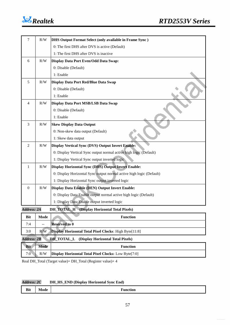
Realtek RTD2553V Series
57
7 R/W DHS Output Format Select (only available in Frame Sync )
0: The first DHS after DVS is active (Default)
1: The first DHS after DVS is inactive
6 R/W Display Data Port Even/Odd Data Swap:
0: Disable (Default)
1: Enable
5 R/W Display Data Port Red/Blue Data Swap
0: Disable (Default)
1: Enable
4 R/W Display Data Port MSB/LSB Data Swap
0: Disable (Default)
1: Enable
3 R/W Skew Display Data Output
0: Non-skew data output (Default)
1: Skew data output
2 R/W Display Vertical Sync (DVS) Output Invert Enable:
0: Display Vertical Sync output normal active high logic (Default)
1: Display Vertical Sync output inverted logic
1 R/W Display Horizontal Sync (DHS) Output Invert Enable:
0: Display Horizontal Sync output normal active high logic (Default)
1: Display Horizontal Sync output inverted logic
0 R/W Display Data Enable (DEN) Output Invert Enable:
0: Display Data Enable output normal active high logic (Default)
1: Display Data Enable output inverted logic
Address: 2A DH_TOTAL_H (Display Horizontal Total Pixels)
Bit Mode Function
7:4 -- Reserved to 0
3:0 R/W Display Horizontal Total Pixel Clocks: High Byte[11:8]
Address: 2B DH_TOTAL_L (Display Horizontal Total Pixels)
Bit Mode Function
7:0 R/W Display Horizontal Total Pixel Clocks: Low Byte[7:0]
Real DH_Total (Target value)= DH_Total (Register value)+ 4
Address: 2C DH_HS_END (Display Horizontal Sync End)
Bit Mode Function
http://www.DataSheet4U.net/
datasheet pdf - http://www.DataSheet4U.net/
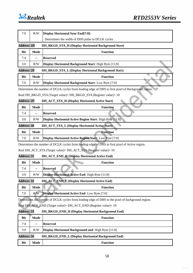
Realtek RTD2553V Series
58
7:0 R/W Display Horizontal Sync End[7:0]:
Determines the width of DHS pulse in DCLK cycles
Address: 2D DH_BKGD_STA_H (Display Horizontal Background Start)
Bit Mode Function
7:4 -- Reserved
3:0 R/W Display Horizontal Background Start: High Byte [11:8]
Address: 2E DH_BKGD_STA_L (Display Horizontal Background Start)
Bit Mode Function
7:0 R/W Display Horizontal Background Start: Low Byte [7:0]
Determines the number of DCLK cycles from leading edge of DHS to first pixel of Background region.
Real DH_BKGD_STA (Target value)= DH_BKGD_STA (Register value)+ 10
Address: 2F DH_ACT_STA_H (Display Horizontal Active Start)
Bit Mode Function
7:4 -- Reserved
3:0 R/W Display Horizontal Active Region Start : High Byte [11:8]
Address: 30 DH_ACT_STA_L (Display Horizontal Active Start)
Bit Mode Function
7:0 R/W Display Horizontal Active Region Start : Low Byte [7:0]
Determines the number of DCLK cycles from leading edge of DHS to first pixel of Active region.
Real DH_ACT_STA (Target value)= DH_ACT_STA (Register value)+ 10
Address: 31 DH_ACT_END_H (Display Horizontal Active End)
Bit Mode Function
7:4 -- Reserved
3:0 R/W Display Horizontal Active End: High Byte [11:8]
Address: 32 DH_ACT_END_L (Display Horizontal Active End)
Bit Mode Function
7:0 R/W Display Horizontal Active End: Low Byte [7:0]
Determines the number of DCLK cycles from leading edge of DHS to the pixel of background region.
Real DH_ACT_END (Target value)= DH_ACT_END (Register value)+ 10
Address: 33 DH_BKGD_END_H (Display Horizontal Background End)
Bit Mode Function
7:4 -- Reserved
3:0 R/W Display Horizontal Background end: High Byte [11:8]
Address: 34 DH_BKGD_END_L (Display Horizontal Background End)
Bit Mode Function
http://www.DataSheet4U.net/
datasheet pdf - http://www.DataSheet4U.net/

Realtek RTD2553V Series
59
7:0 R/W Display Horizontal Background end: Low Byte [7:0]
Real DH_BKGD_END (Target value) = DH_BKGD_END (Register value)+ 10
Address: 35 DV_TOTAL_H (Display Vertical Total Lines)
Bit Mode Function
7:4 -- Reserved to 0
3:0 R/W Display Vertical Total: High Byte [11:8]
Address: 36 DV_TOTAL_L (Display Vertical Total Lines)
Bit Mode Function
7:0 R/W Display Vertical Total: Low Byte [7:0]
CR35, CR36 use as watch dog reference value in frame sync mode, the event should be the line number of
display HS is equal to DV Total.
Address: 37 DVS_END (Display Vertical Sync End)
Bit Mode Function
7:5 -- Reserved
4:0 R/W Display Vertical Sync End[4:0]:
Determines the duration of DVS pulse in lines
Address: 38 DV_BKGD_STA_H (Display Vertical Background Start)
Bit Mode Function
7:4 -- Reserved
3:0 R/W Display Vertical Background Start: High Byte [11:8]
Determines the number of lines from leading edge of DVS to first line of background region.
Address: 39 DV_BKGD_STA_L (Display Vertical Background Start)
Bit Mode Function
7:0 R/W Display Vertical Background Start: Low Byte [7:0]
Address: 3A DV_ACT_STA_H (Display Vertical Active Start)
Bit Mode Function
7:4 -- Reserved
3:0 R/W Display Vertical Active Region Start: High Byte [11:8]
Determines the number of lines from leading edge of DVS to first line of active region.
Address: 3B DV_ACT_STA_L (Display Vertical Active Start)
Bit Mode Function
7:0 R/W Display Vertical Active Region Start: Low Byte [7:0]
Address: 3C DV_ACT_END_H (Display Vertical Active End)
Bit Mode Function
7:4 -- Reserved
http://www.DataSheet4U.net/
datasheet pdf - http://www.DataSheet4U.net/
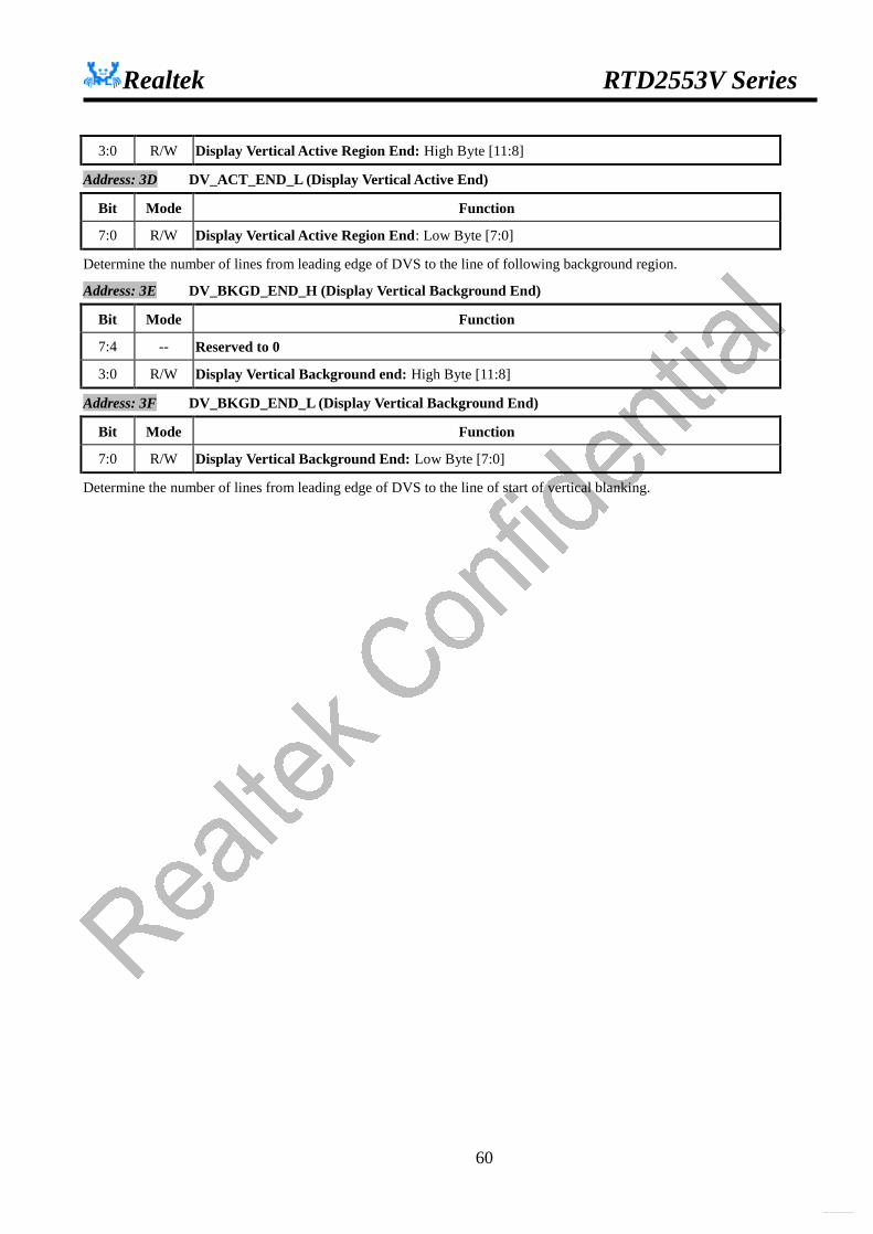
Realtek RTD2553V Series
60
3:0 R/W Display Vertical Active Region End: High Byte [11:8]
Address: 3D DV_ACT_END_L (Display Vertical Active End)
Bit Mode Function
7:0 R/W Display Vertical Active Region End: Low Byte [7:0]
Determine the number of lines from leading edge of DVS to the line of following background region.
Address: 3E DV_BKGD_END_H (Display Vertical Background End)
Bit Mode Function
7:4 -- Reserved to 0
3:0 R/W Display Vertical Background end: High Byte [11:8]
Address: 3F DV_BKGD_END_L (Display Vertical Background End)
Bit Mode Function
7:0 R/W Display Vertical Background End: Low Byte [7:0]
Determine the number of lines from leading edge of DVS to the line of start of vertical blanking.
http://www.DataSheet4U.net/
datasheet pdf - http://www.DataSheet4U.net/

Realtek RTD2553V Series
61
Frame Sync Fine Tune Address: 40 IVS2DVS_DEALY_LINES (IVS to DVS Lines) Default: 00h
Bit Mode Function
7:0 R/W IVS to DVS Lines: (Only for FrameSync Mode)
The number of input HS from IVS to DVS.
Should be double buffer by CR05[5:4]
Address: 41 IV_DV_DELAY_CLK_ODD (Frame Sync Delay Fine Tuning) Default: 00h
Bit Mode Function
7:0 R/W Frame Sync Mode Delay Fine Tune [7:0] “00” to disable
Applied to all fields when Interlaced_FS_Delay_Fine_Tuning is disabled (CR43[1] = 0)
Only for odd-field when Interlaced_FS_Delay_Fine_Tuning is enabled (CR43[1] = 1)
In Frame Sync Mode , CR40[7:0] represents output VS delay fine-tuning. For example, it delays the number of
(CR41 [7:0] *16 + 16) input clocks. Fill 00h, means 0, fill 01h, and means 32
Address: 42 IV_DV_DELAY_CLK_EVEN (Frame Sync Delay Fine Tuning) Default: 00h
Bit Mode Function
7:0 R/W Frame Sync Mode Delay Fine Tune [7:0] “00” to disable
Only for even-field when Interlaced_FS_Delay_Fine_Tuning is enabled (CR43[1] = 1)
Address: 43 FS_DELAY_FINE_TUNING Default: 00h
Bit Mode Function
7:2 R/W Reserved to 0
1 R/W Interlaced_FS_Delay_Fine_Tuning
0: Disable (Default)
1: Enable
0 R/W Internal ODD-signal inverse for Interlaced_FS_Delay_Fine_Tuning
0: No invert (Default)
1: Invert
Address: 44 LAST_LINE_H Default: 00h
Bit Mode Function
7 R/W Last-line-width / DV-Total Selector :
0: CR44 [3:0] and CR45 indicate last-line width counted by display clock (Default)
1: CR44 [3:0] and CR45 indicate DHS total number between 2 DVS.
6 R/W DV sync with 4X clock
0: Disable
1: Enable
5 R/W BIST Test Enable
0: Disable
http://www.DataSheet4U.net/
datasheet pdf - http://www.DataSheet4U.net/

Realtek RTD2553V Series
62
1: Enable (Auto clear when finish)
4 R/W BIST Test Result
0: Fail
1: Ok
3:0 R DV Total or Last Line Width[11:8] Before Sync in Frame Sync Mode
Address: 45 LAST_LINE_L
Bit Mode Function
7:0 R DV Total or Last Line Width[7:0] Before Sync in Frame Sync Mode
Display Fine Tune Address: 46 DIS_TIMING (Display Clock Fine Tuning Register) Default: 00h
Bit Mode Function
7 R/W Reserved to 0
6:4 R/W Display Output Clock Fine Tuning Control:
000: DCLK rising edge correspondents with output display data
001: 1ns delay
010: 2ns delay
011: 3ns delay
100: 4ns delay
101: 5ns delay
110: 6ns delay
111: 7ns delay
3 R/W ACLK/BCLK Output Enable ( Only used in 6 bit TTL/smart panel, otherwise, use DCLK)
0: Disable
1: Enable
2 R/W ACLK(6 bit)/DCLK(8 bit) Polarity Inverted
0: Disable
1: Enable
1 R/W DCLK Output Enable (Only been used in TTL 8 bit mode)
0: Disable
1: Enable
0 R/W BCLK(6 bit) Polarity Inverted
0: Non-Inverted
1: Inverted
http://www.DataSheet4U.net/
datasheet pdf - http://www.DataSheet4U.net/
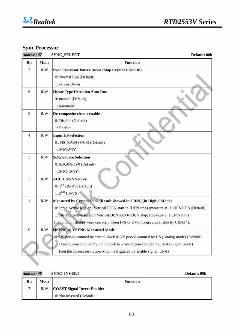
Realtek RTD2553V Series
63
Sync Processor Address: 47 SYNC_SELECT Default: 00h
Bit Mode Function
7 R/W Sync Processor Power Down (Stop Crystal Clock In)
0: Normal Run (Default)
1: Power Down
6 R/W Hysnc Type Detection Auto Run
0: manual (Default)
1: automatic
5 R/W De-composite circuit enable
0: Disable (Default)
1: Enable
4 R/W Input HS selection
0 : HS_RAW(SS/CS) (Default)
1: SOG/SOY
3 R/W SOG Source Selection
0: SOG0/SOY0 (Default)
1: SOG1/SOY1
2 R/W ADC HS/VS Source
0: 1ST HS/VS (Default)
1: 2ND HS/VS
1 R/W Measured by Crystal clock (Result showed in CR59) (in Digital Mode)
0: Input Active Region (Vertical IDEN start to IDEN stop) (measure at IDEN STOP) (Default)
1: Display Active Region(Vertical DEN start to DEN stop) (measure at DEN STOP)
The function should work correctly when IVS or DVS occurs and enable by CR50[4].
0 R/W HSYNC & VSYNC Measured Mode
0: HS period counted by crystal clock & VS period counted by HS (Analog mode) (Default)
1: H resolution counted by input clock & V resolution counted by ENA (Digital mode)
(Get the correct resolution which is triggered by enable signal, ENA)
Address: 48 SYNC_INVERT Default: 00h
Bit Mode Function
7 R/W COAST Signal Invert Enable:
0: Not inverted (Default)
http://www.DataSheet4U.net/
datasheet pdf - http://www.DataSheet4U.net/
Realtek RTD2553V Series
64
1: Inverted
6 R/W COAST Signal Output Enable:
0: Disable (Default)
1: Enable
5 R/W HS_OUT Signal Invert Enable:
0: Not inverted (Default)
1: Inverted
4 R/W HS_OUT Signal Output Enable:
0: Disable (Default)
1: Enable
3 R/W CS_RAW Inverted Enable
0: Normal (Default)
1: Invert
2 R/W CLAMP Signal Output Enable
0: Disable (Default)
1: Enable
1 R/W HS Recovery in Coast
0: Disable (Default) (SS/SOY)
1: Enable (CS or SOG )
0 R/W HSYNC Synchronize source
0: AHS (Default)
1: Feedback HS
Address: 49 SYNC_CTRL (SYNC Control Register) Default: 02h
Bit Mode Function
7 R/W CLK Inversion to latch Feedback HS for Coast Recovery
( Coast Recovery means HS feedback to replace input HS)
0: Non Inversion (Default)
1: Inversion
6 R/W Select HS_OUT Source Signal
0: Bypass (SeHs)(Use in Separate Mode)
1: Select De-Composite HS out(DeHs) (In Composite mode)
5 R/W Select ADC_VS Source Signal (Auto switch in Auto Run Mode)
0: VS_RAW
1: DeVS
4 R/W CLK Inversion to latch ADC HS for Clamp
0: Non Inversion (Default)
http://www.DataSheet4U.net/
datasheet pdf - http://www.DataSheet4U.net/

Realtek RTD2553V Series
65
1: Inversion
3 R/W Inversion of HS to measure Vsync
0: Non Inversion (Default)
1: Inversion
2 R/W HSYNC Measure Source(ADC_HS)
0: Select ADC_HS (Default)
1: Select SeHS or DeHS by CR49[6]
1:0 R/W Measure HSYNC/VSYNC Source Select:
00: TMDS
01: VIDEO8/VIDEO16
10: ADC_HS1/ADC_VS (Default)
11: CS_RAW/VS_RAW
Address: 4A STABLE_HIGH_PERIOD_H
Bit Mode Function
7 R Even/Odd Field of YPbPr
0: Even
1: Odd
6 R The toggling of polarity of YPbPr Field happens
0: No toggle
1: Toggle
5:3 R The number of input HS between 2 input VSYNC.
LSB bit [2:0] for YPbPr
2:0 R Stable High Period[10:8]
Compare each line’s high pulse period, if we get continuous 64 lines with the same one, the
period is updated as the stable period.
Address: 4B STABLE_HIGH_PERIOD_L Bit Mode Function 7:0 R Stable High Period[7:0]
Compare each line’s high pulse period, if we get continuous 64 lines with the same one, the period is updated as the stable period.
Address: 4C VSYNC_COUNTER_LEVEL_MSB Default: 03h
Bit Mode Function
7 R Hysnc Type Detection Auto Run Result ready
6:4 R Hysnc Type Detection Auto Run Result 000: No Signal
001: Not Support
http://www.DataSheet4U.net/
datasheet pdf - http://www.DataSheet4U.net/

Realtek RTD2553V Series
66
010: YPbPr
011: Serration Composite SYNC
100: XOR/OR-Type Composite SYNC with Equalizer
101: XOR/OR-Type Composite SYNC without Equalizer
110: HSYNC with VS_RAW (Separate HSYNC)
111: HSYNC without VS_RAW (HSYNC only)
Reference when Hsync type detection auto run result ready (CR4C[7]) 3 R/W 2nd ADC/Video switch
0: 2ND ADC (Default)
1: Video8
2:0 R/W Vsync counter level count [10:8] MSB
Vsync detection counter start value.
Address: 4D VSYNC_COUNTER_LEVEL_LSB Default: 00h
Bit Mode Function
7:0 R/W Vsync counter level count [7:0] LSB
Address: 4E HSYNC_TYPE_DETECTION_FLAG
Bit Mode Function
7 R HS Overflow(16-bits)
6 R Stable Period Change (write clear when CR4E[6]=1 or CR4F[0]=1)
5 R Stable Polarity Change (write clear when CR4E[5]=1 or CR4F[0]=1)
4 R VS_RAW Edge Occurs (Only use in Auto Run Mode)
If VS_RAW edge occurs, this bit is set to “1”.
3 R Detect Capture Window Unlock repeated 32 times (write clear when CR4E[3]=1 or
CR4F[0]=1)
2 R HSYNC have Equalization (write clear when CR4E[2]=1 or CR4F[0]=1)
1 R HSYNC Polarity Change (write clear when CR4E[1]=1 or CR4F[0]=1)
0 R Detect Capture Window Unlock (write clear when CR4E[0]=1 or CR4F[0]=1)
Address: 4F STABLE_MEASURE Default: 00h
Bit Mode Function
7 R Stable Flag
0: Period or polarity can’t get continuous stable status.
1: Both polarity and period are stable.
6 R Stable Polarity
0: Negative
http://www.DataSheet4U.net/
datasheet pdf - http://www.DataSheet4U.net/
Realtek RTD2553V Series
67
1: Positive
Compare each line’s polarity; if we get continuous N 64 lines with the same one, the polarity is
updated as the stable polarity.
5:4 R/W Feedback Hsync High Period Select by ADC Clock:
00: 32 (Default)
01: 64
10: 96
11: 128
3 R/W Stable Period Tolerance
0: ±2 crystal clks (Default)
1: ±4 crystal clks
2 R/W Vsync measure invert Enable
0: Disable (Default)
1: Enable
1 R/W Pop Up Stable Value
0: No Pop Up (Default)
1: Pop Up Result, (CR4A[2:0], CR4B[7:0], CR4E[3], CR50[2:0], CR51[7:0])
0 R/W Stable Measure Start
0 : Stop (Default)
1 : Start
Address: 50 Stable_Period_H Default: 00h
Bit Mode Function
7 -- Reserved
6 R CS_RAW Inverted by Auto Run Mode
0: Not inverted
1: Inverted
5 R/W HS_OUT Bypass PLL into VGIP
0: Disable (Default)
1: Enable
4 R/W Active Region Measure Enable
0: Disable (Default)
1: Enable
3 R/W ADC_VS Source Select in Test Mode
0: Select ADC_VS Source in Normal Mode or Auto Mode by CR47[6] (Default)
1: Select ADC_VS Source in Test Mode (Select VS_RAW or DeVS by CR49[5])
2:0 R Stable Period[10:8]
http://www.DataSheet4U.net/
datasheet pdf - http://www.DataSheet4U.net/
Realtek RTD2553V Series
68
Compare each line’s period, if we get continuous 64 lines with the same one, the period is updated
as the stable period.
Address: 51 Stable_Period_L
Bit Mode Function
7:0 R Stable Period[7:0]
Compare each line’s period, if we get continuous 64 lines with the same one, the period is updated
as the stable period.
Address: 52 MEAS_HS_PER_H (HSYNC Period Measured Result) Default: 8’b000xxxxx
Bit Mode Function
7 R/W On Line Auto Measure Enable
0: Disable (Default)
1: Enable
6 R/W Pop Up Period Measurement Result
0: No Pop Up (Default)
1: Pop Up Result
5 R/W Start a HS & VS period / H & V resolution & polarity measurement (on line monitor)
0: Finished/Disable (Default)
1: Enable to start a measurement, auto cleared after finished
4 R Over-flow bit of Input HSYNC Period Measurement
0: No Over-flow occurred
1: Over-flow occurred
3:0 R Input HSYNC Period Measurement Result: High Byte[11:8]
Address: 53 MEAS_HS_PER_L (HSYNC Period Measured Result)
Bit Mode Function
7:0 R Input HSYNC Period Measurement Result: Low Byte[7:0]
l This result is expressed in terms of crystal clocks.
l When measured digitally, the result is expressed as the number of input clocks between 2 input HS signals
Address: 54 MEAS_VS_PER_H (VSYNC Period Measured Result)
Bit Mode Function
7 R Input VSYNC Polarity Indicator
0: negative polarity (high period is longer than low one)
1: positive polarity (low period is longer than high one)
6 R Input HSYNC Polarity Indicator
0: negative polarity (high period is longer than low one)
1: positive polarity (low period is longer than high one)
5 R Time-Out bit of Input VSYNC Period Measurement (No VSYNC occurred)
http://www.DataSheet4U.net/
datasheet pdf - http://www.DataSheet4U.net/

Realtek RTD2553V Series
69
0: No Time Out
1: Time Out occurred
4 R Over-flow bit of Input VSYNC Period Measurement
0: No Over-flow occurred
1: Over-flow occurred
3:0 R Input VSYNC Period Measurement Result: High Byte[11:8]
Address: 55 MEAS_VS_PER_L (VSYNC Period Measured Result)
Bit Mode Function
7:0 R Input VSYNC Period Measurement Result: Low Byte[7:0]
l This result is expressed in terms of input HS pulses.
l When measured digitally, the result is expressed as the number of input ENA signal within a frame.
Address: 56 MEAS_HS&VS_HI_H (HSYNC&VSYNC High Period Measured Result)
Bit Mode Function
7:4 R Input HSYNC High Period Measurement Result: High Byte[11:8]
3:0 R Input VSYNC High Period Measurement Result: High Byte[11:8]
Address: 57 MEAS_HS_HI_L (HSYNC High Period Measured Result)
Bit Mode Function
7:0 R Input HSYNC High Period Measurement Result: Low Byte[7:0]
This result is expressed in terms of crystal clocks. When measured digitally, the result is expressed as the number of
input clocks inside the input enable signal
Address: 58 MEAS_VS_HI_L (VSYNC High Period Measured Result)
Bit Mode Function
7:0 R Input VSYNC High Period Measurement Result: Low Byte[7:0]
This result is expressed in terms of input HS pulses
Address: 59 MEAS_ACTIVE_REGION_H (Active Region Measured by CRSTL_CLK Result)
Bit Mode Function
7:0 R/W Active Region Measured By Crystal Clock
1st read: Measurement Result: High Byte[23:16]
2nd read: Measurement Result: High Byte[15:8]
3rd read: Measurement Result: High Byte[8:0]
Read pointer is auto increase, if write, the pointer is also reset to 1 st result.
Address: 5A CLAMP_START (Clamp Signal Output Start) Default: 04h
Bit Mode Function
7:0 R/W Start of Output Clamp Signal Pulse[7:0]:
Determine the number of input double-pixel between the trailing edge of input
HSYNC and the start of the output CLAMP signal.
http://www.DataSheet4U.net/
datasheet pdf - http://www.DataSheet4U.net/

Realtek RTD2553V Series
70
Address: 5B CLAMP_END (Clamp Signal Output End) Default: 10h
Bit Mode Function
7:0 R/W End of Output Clamp Signal Pulse[7:0]:
Determine the number of input double-pixel between the trailing edge of input
HSYNC and the end of the output CLAMP signal.
Address: 5C Clamp_CTRL0 Default:00h
Bit Mode Function
7 R/W Clamp Mask Enable
0: Disable (Disable)
1: Enable
6 R/W CLAMP_Trigger_Edge_Inverse
0: Trailing edge (Disable)
1: Leading edge
5:0 R/W Mask Line Number before DeVS [5:0]
Address: 5D Clamp_CTRL1 Default: 00h
Bit Mode Function
7 R/W Sync Processor Test Mode
0: Normal (Default)
1: Enable Test Mode; (switch 70ns-ck to the time-out & polarity counters)
6 R/W Select Clamp Mask as De VS
0: Disable
1: Enable
5:0 R/W Mask Line Number after DeVS [5:0]
CR5C[5:0] and CR5D[5:0] will set number of Mask Line before/after DeVS for COAST, Clamp Mask, and CR5D[6].
Macro Vision Address: 5E Macro Vision Control Default: 00h
Bit Mode Function
7:4 R/W Skip Line[3:0]
Skip Lines after Vsync detected
3 R/W Test-Mode for Clamp, HS_RAW is directly from PAD
0: Clamp source from normal HS
1: Clamp source from HS_RAW
2 R/W Odd Detection Mode
http://www.DataSheet4U.net/
datasheet pdf - http://www.DataSheet4U.net/
Realtek RTD2553V Series
71
0: Line Count (Default)
1: VS Position
1 R MacroVision Detected (On-line monitor)
When detected macrovision occurred, this bit set to 1, else clear to 0.
0 R/W Macro Vision Enable
0: Disable (Default)
1: Enable
Highlight window Address: 60 highlight window access port control Default: 00h
Bit Mode Function
7 R/W Enable highlight window access port
6 R/W Enable highlight window
5:4 -- Reserved
3:0 R/W Highlight-window port address
Address: 61-00 highlight window horizontal start
Bit Mode Function
7:0 -- Reserved
2:0 R/W highlight window horizontal start[10:8]
Address: 61-01 highlight window horizontal start
Bit Mode Function
7:0 R/W highlight window horizontal start[7:0]
Address: 61-02 highlight window horizontal end
Bit Mode Function
7:3 -- Reserved
2:0 R/W highlight window horizontal end[10:8]
Address: 61-03 highlight window horizontal end
Bit Mode Function
7:0 R/W highlight window horizontal end[7:0]
Address: 61-04 highlight window vertical start
http://www.DataSheet4U.net/
datasheet pdf - http://www.DataSheet4U.net/
Realtek RTD2553V Series
72
Bit Mode Function
7:3 -- Reserved
2:0 R/W highlight window vertical start[10:8]
Address: 61-05 highlight window vertical start
Bit Mode Function
7:0 R/W highlight window vertical start[7:0]
Address: 61-06 highlight window vertical end
Bit Mode Function
7:3 -- Reserved
2:0 R/W highlight window vertical end[10:8]
Address: 61-07 highlight window vertical end
Bit Mode Function
7:0 R/W highlight window vertical end[7:0]
Highlight window horizontal/vertical reference point is DEN (display background start).
Address: 61-08 highlight window border
Bit Mode Function
7:4 -- Reserved
3:0 R/W highlight window border width
Address: 61-09 highlight window border color
Bit Mode Function
7:6 -- Reserved
5:0 R/W highlight window border red color MSB 6bit (red color 2-bit LSB = 00)
Address: 61-0A highlight window border color
Bit Mode Function
7:6 -- Reserved
5:0 R/W highlight window border green color MSB 6bit (green color 2-bit LSB = 00)
Address: 61-0B highlight window border color
Bit Mode Function
7:6 -- Reserved
5:0 R/W highlight window border blue color MSB 6bit (blue color 2-bit LSB = 00)
http://www.DataSheet4U.net/
datasheet pdf - http://www.DataSheet4U.net/

Realtek RTD2553V Series
73
Address: 61-0C highlight window control default : 00h
Bit Mode Function
7:6 R/W Contrast / brightness application control
00: Set A used on full region
01: Set B used inside highlight window
10: Set A used outside highlight window
11: Set A used outside highlight window, and Set B used inside highlight window
Contrast
(CR62[1])
Application control Inside window Outside window
0 X bypass bypass
1 CR61-0C[7:6]=00 || CR60[6]=0 Set A Set A
1 CR61-0C[7:6]=01 && CR60[6]=1 Set B bypass
1 CR61-0C[7:6]=10 && CR60[6]=1 bypass Set A
1 CR61-0C[7:6]=11 && CR60[6]=1 Set B Set A
Brightness
(CR62[0])
Application control Inside window Outside window
0 X bypass bypass
1 CR61-0C[7:6]=00 || CR60[6]=0 Set A Set A
1 CR61-0C[7:6]=01 && CR60[6)=1 Set B bypass
1 CR61-0C[7:6]=10 && CR60[6]=1 bypass Set A
1 CR61-0C[7:6]=11 && CR60[6]=1 Set B Set A 5:4 R/W Gamma application control
00 : gamma used on full region
01: gamma used inside window
10: gamma used outside window
11: reserved
Gamma
(CR67[6])
Application control Inside window Outside window
0 X bypass bypass
1 CR61-0C[5:4]=00 || CR60[6]=0 Gamma Gamma
1 CR61-0C[5:4]=01 && CR60[6]=1 Gamma bypass
1 CR61-0C[5:4]=10 && CR60[6]=1 bypass Gamma
3:2 R/W SRGB/DCC/ICM application control
http://www.DataSheet4U.net/
datasheet pdf - http://www.DataSheet4U.net/

Realtek RTD2553V Series
74
00 : SRGB/DCC/ICM used on full region
01: SRGB/DCC/ICM used inside window
10: SRGB/DCC/ICM used outside window
11: reserved
SRGB
(CR62[2])
Application control Inside window Outside window
0 X bypass bypass
1 CR61-0C[3:2]=00 || CR60[6]=0 SRGB SRGB
1 CR61-0C[3:2]=01 && CR60[6]=1 SRGB bypass
1 CR61-0C[3:2]=10 && CR60[6]=1 bypass SRGB
ICM
(CRE0[7])
Application control Inside window Outside window
0 X bypass bypass
1 CR61-0C[3:2]=00 || CR60[6]=0 ICM ICM
1 CR61-0C[3:2]=01 && CR60[6]=1 ICM bypass
1 CR61-0C[3:2]=10 && CR60[6]=1 bypass ICM
DCC
(CRE4[7])
Application control Inside window Outside window
0 X bypass bypass
1 CR61-0C[3:2]=00 || CR60[6]=0 DCC DCC
1 CR61-0C[3:2]=01 && CR60[6]=1 DCC bypass
1 CR61-0C[3:2]=10 && CR60[6]=1 bypass DCC
1:0 -- Reserved
h t t p : / / w w w . D a t a S h e e t 4 U . n e t /
d a t a s h e e t p d f - h t t p : / / w w w . D a t a S h e e t 4 U . n e t /

Realtek RTD2553V Series
75
Inside window left-top point = (horizontal start + border width, vertical start + border width) Inside window right-bottom point = (horizontal end, vertical end) Border window left-top point = (horizontal start, vertical start) Border window right-bottom point = (horizontal end+ border width, vertical end + border width) Border = border window – inside window Outside window = screen – border window
Color Processor Control Address: 62 COLOR_CTRL (Color Control Register) Default: 00h
Bit Mode Function
7 -- Reserved to 0
6 R/W sRGB precision
0: Normal (Default)
1: 1 bit shift
5:3 R/W sRGB Coefficient Write Enable
000: Disable
001: Write R Channel (RRH,RRL,RGH,RGL,RBH,RBL) (address reset to 0 when written)
(horizontal start, vertical start)
(horizontal end, vertical end)
Border width
Inside window
border
http://www.DataSheet4U.net/
datasheet pdf - http://www.DataSheet4U.net/
Realtek RTD2553V Series
76
010: Write G Channel (GRH,GBL,GGH,GGL,GBH,GBL) (address reset to 0 when written)
011: Write B Channel (BRH,BRL,BGH,BGL,BBH,BBL) (address reset to 0 when written)
100: R Offset
101: G Offset
110: B Offset
2 R/W Enable sRGB Function
0: Disable (Default)
1: Enable
1 R/W Enable Contrast Function:
0: disable the coefficient (Default)
1: enable the coefficient
0 R/W Enable Brightness Function:
0: disable the coefficient (Default)
1: enable the coefficient
Address: 63 SRGB_ACCESS_PORT
Bit Mode Function
7:0 W sRGB_COEF[7:0]
+++
++
+=
BoffsetBGoffsetGRoffsetR
BBBGBRGBGGGRRBRGRR
BGR
11
1
'
'
'
Brightness Coefficient: Address: 64 Contrast /Brightness Access Port Control Default: 00h
Bit Mode Function
7 R/W Enable Contrast /Brightness access port
6:4 -- Reserved
3:0 R/W Contrast /Brightness port address
Access data port continuously will get address auto increase. Address: 65-00 BRI_RED_COE (Set A)
Bit Mode Function
7:0 R/W Brightness Red Coefficient:
Valid range: -128(00h) ~ 0(80h) ~ +127(FFh)
Address: 65-01 BRI_GRN_COE (Set A)
Bit Mode Function
7:0 R/W Brightness Green Coefficient: Valid range:
http://www.DataSheet4U.net/
datasheet pdf - http://www.DataSheet4U.net/
Realtek RTD2553V Series
77
Valid range: -128(00h) ~ 0(80h) ~ +127(FFh)
Address: 65-02 BRI_BLU_COE (Set A)
Bit Mode Function
7:0 R/W Brightness Blue Coefficient:
Valid range: -128(00h) ~ 0(80h) ~ +127(FFh)
Address: 65-03 CTS_RED_COE (Set A)
Bit Mode Function
7:0 R/W Contrast Red Coefficient:
Valid range: 0(00h) ~ 1(80h) ~ 2(FFh)
Address: 65-04 CTS_GRN_COE (Set A)
Bit Mode Function
7:0 R/W Contrast Green Coefficient:
Valid range: 0(00h) ~ 1(80h) ~ 2(FFh)
Address: 65-05 CTS_BLU_COE (Set A)
Bit Mode Function
7:0 R/W Contrast Blue Coefficient:
Valid range: 0(00h) ~ 1(80h) ~ 2(FFh)
Address: 65-06 BRI_RED_COE (Set B)
Bit Mode Function
7:0 R/W Brightness Red Coefficient:
Valid range: -128(00h) ~ 0(80h) ~ +127(FFh)
Address: 65-07 BRI_GRN_COE (Set B)
Bit Mode Function
7:0 R/W Brightness Green Coefficient: Valid range:
Valid range: -128(00h) ~ 0(80h) ~ +127(FFh)
Address: 65-08 BRI_BLU_COE (Set B)
Bit Mode Function
7:0 R/W Brightness Blue Coefficient:
Valid range: -128(00h) ~ 0(80h) ~ +127(FFh)
Address: 65-09 CTS_RED_COE (Set B)
Bit Mode Function
7:0 R/W Contrast Red Coefficient:
Valid range: 0(00h) ~ 1(80h) ~ 2(FFh)
Address: 65-0A CTS_GRN_COE (Set B)
http://www.DataSheet4U.net/
datasheet pdf - http://www.DataSheet4U.net/

Realtek RTD2553V Series
78
Bit Mode Function
7:0 R/W Contrast Green Coefficient:
Valid range: 0(00h) ~ 1(80h) ~ 2(FFh)
Address: 65-0B CTS_BLU_COE (Set B)
Bit Mode Function
7:0 R/W Contrast Blue Coefficient:
Valid range: 0(00h) ~ 1(80h) ~ 2(FFh)
When highlight window is disable, coefficient set A is used.
Gamma Control Address: 66 GAMMA_PORT
Bit Mode Function
7:0 W Access port for gamma correction table
l The input data sequence is {g0[9:2]}, {g0[1:0], 1’b0, d0[4:0]}, {3’b0, d1[4:0]}; {g2[9:2]}, {g2[1:0], 1’b0,
d2[4:0]}, {3’b0, d3[4:0]}; … ; {g254[9:2]}, {g254[1:0] , 1’b0, d254[4:0]}, {3’b0, d255[4:0]} for full gamma
table.
l The input data sequence is {g0[9:2]}, {g0[1:0], 1’b0, d0[4:0]}, {g2[9:2]}, {g2[1:0] , 1’b0, d2[4:0]} … ,
{g254[9:2]}, {g254[1:0] ,1’b0, d254[4:0] } for compact gamma table.
l For compact gamma table, d1[4:0]=d0[4:0], d3[4:0]=d2[4:0], … , d(2n+1)[4:0]=d(2n)[4:0].
l g(n) is 10bit gamma coefficient, and d(n) is g(n+1) – g(n) with 5bit.
l If n is even, Gamma-port output is g(n) + d(n)*(2bit LSB brightness output)/4.
l If n is odd, Gamma-port output is g(n-1) + d(n-1) + d(n)*(2bit LSB brightness output)/4.
l Gamma can be only accessed when DCLK exists.
l The latest stage of d[n] can’t let gamma curve exceed 255. Address: 67 GAMMA_CTRL Default: 00h
Bit Mode Function 7 R/W Enable Access Channels for Gamma Correction Coefficient:
0: disable these channels (Default)
1: enable these channels 6 R/W Gamma table enable
0: by pass (Default)
1: enable 5:4 R/W Color Channel of Gamma Table
00: Red Channel (Default)
01: Green Channel
10: Blue Channel
11: Red/Green/Blue Channel (R/G/B Gamma are the same)
http://www.DataSheet4U.net/
datasheet pdf - http://www.DataSheet4U.net/

Realtek RTD2553V Series
79
3:1 -- Reserved to 0 0 R/W Gamma Access Type
0: access compact gamma table (Default)
1: access full gamma table l Access Gamma_Access register will reset GAMMA_PORT index. Address: 68 GAMMA_BIST (Color Control Register) Default: 00h
Bit Mode Function 7 R/W Test_mode
0: Disable, dither_out = dither_result[9:2]; // truncate to integer number (Default)
1: Enable, dither_out = dither_result[7:0]; // propagate decimal part for test 6:4 -- Reserved to 0 3:2 R/W Gamma BIST select
00: BIST Disable (Default)
01: Red LUT
10: Green LUT
11: Blue LUT 1 R/W Gamma BIST_Progress
0: BIST is done (Default)
1: BIST is running 0 R Gamma BIST Test Result
0: SRAM Fail
1: SRAM OK
Dithering Control Address: 69 DITHERING_SEQUENCE_TABLE
Bit Mode Function
7:6 W Dithering Sequence Table (SR3)
5:4 W Dithering Sequence Table (SR2)
3:2 W Dithering Sequence Table (SR1)
1:0 W Dithering Sequence Table (SR0)
l There are three set of dithering sequence table, each table contains 32 elements, s0, s1, … , s31.
Each element has 2 bit to index one of 4 dithering table.
l Input data sequence is {sr3,sr2,sr1,sr0}, {sr7,sr6,sr5,sr4}, … , {sr31,sr30,sr29,sr28}, {sg3,sg2,sg1,sg0}, … ,
{sg31,sg30,sg29,sg28}, {sb3,sb2,sb1,sb0}, … , {sb31,sb30,sb29,sb28} for red, green and blue channel.
l R + (2R+1) * C choose sequence element, where R is Row Number / 2, and C is Column Number / 2. Address: 6A DITHERING_TABLE_ACCESS (Dithering Table Access Port)
Bit Mode Function
7:4 W Access port for dithering table D00/D02/ D10/D12/D20/D22/D30/D32
3:0 W Access port for dithering table D01/D03/ D11/D13/D21/D23/D31/D33
l Red, green, blue each channel has 4 dithering table, each table is 2x2 elements, and one element has 4 bit
for 10B/8B, the elements should fill 0 to 3, for 10B/6B, the elements should fill 0 to 15.
http://www.DataSheet4U.net/
datasheet pdf - http://www.DataSheet4U.net/
Realtek RTD2553V Series
80
l Input data sequence is [Dr00 Dr01],[Dr02,Dr03], … , [Dr30,Dr31],[Dr32,Dr33], [Dg00,Dg01],[Dg02,Dg03], … ,
[Dg30,Dg31],[Dg32,Dg33], [Db00,Db01],[Db02,Db03], … , [Db30,Db31],[Db32,Db33].
D00 D01 D10 D11 D20 D21 D30 D31
D02 D03 D12 D13 D22 D23 D32 D33 Address: 6B DITHERING_CTRL Default: 00h
Bit Mode Function 7 R/W Enable Access Dithering Sequence Table
0: disable (Default)
1: enable 6 R/W Enable Access Dithering Table
0: disable (Default)
1: enable 5 R/W Enable Dithering Function
0: disable (Default)
1: enable 4 R/W Temporal Dithering
0: Disable (Default)
1: Enable
3 R/W Dithering Table Value Sign
0: unsigned
1: signed (2’s complement)
2 R/W Dithering Mode
0: New (Default)
1: Old
1 R/W Vertical Frame Modulation
0: Disable (Default)
1: Enable
0 R/W Horizontal Frame Modulation
0: Disable (Default)
1: Enable
l {Dithering sequence + Frame Number (if temporal dithering)} mod 4 determine which dithering table to use
http://www.DataSheet4U.net/
datasheet pdf - http://www.DataSheet4U.net/
Realtek RTD2553V Series
81
Overlay/Color Palette/Background Color Control Address: 6C OVERLAY_CTRL (Overlay Display Control Register) Default: 00h
Bit Mode Function
7:6 -- Reserved to 0
5 R/W Background color access enable
0: Disable(Reset CR6D Write Pointer to R)
1: Enable
4:2 R/W Alpha blending level (Also enable OSD frame control register 0x003 byte 1[3:2]
000: Disable (Default)
001 ~111: 1/8~ 7/8
1 R/W Overlay Sampling Mode Select:
0: single pixel per clock (Default)
1: dual pixels per clock (The OSD will be zoomed 2X in horizontal scan line)
0 R/W Overlay Port Enable:
0: Disable (Default)
1: Enable
Turn off overlay enable and switch to background simultaneously when auto switch to
background.
Address: 6D BGND_COLOR_CTRL Default: 00h
Bit Mode Function
7:0 R/W Background color RGB 8-bit value[7:0]
l There are 3 bytes color select of background R, G, B, once we enable Background color access channel(CR6C[5]
and the continuous writing sequence is R/G/B
Address: 6E OVERLAY_LUT_ADDR (Overlay LUT Address) Default: 00h
Bit Mode Function
7 R/W Enable Overlay Color Plate Access:
0: Disable (Default)
1: Enable
6 R/W Reserved to 0
5:0 R/W Overlay 16x24 Look-Up-Table Write Address [5:0]
l Auto-increment while every accessing “Overlay LUT Access Port”.
Address: 6F COLOR_LUT_PORT (LUT Access Port)
Bit Mode Function
7:0 W Color Palette 16x24 Look-Up-Table access port [7:0]
l Using this port to access overlay color plate which addressing by the above registers.
l The writing sequence into LUT is [R0, G0, B0, R1, G1, B1, … R15, G15, and B15] and the address counter will
http://www.DataSheet4U.net/
datasheet pdf - http://www.DataSheet4U.net/
Realtek RTD2553V Series
82
be automatic increment and circular from 0 to 47.
Image Auto Function Address: 70 H_BOUNDARY_H
Bit Mode Function
7 -- Reserved
6:4 R/W Horizontal Boundary Start: High Byte [10:8]
3:0 R/W Horizontal Boundary End: High Byte [11:8]
Address: 71 H_BOUNDARY_STA_L
Bit Mode Function
7:0 R/W Horizontal Boundary Start: Low Byte [7:0]
Address: 72 H_BOUNDARY_END_L
Bit Mode Function
7:0 R/W Horizontal Boundary End: Low Byte [7:0]
Address: 73 V_BOUNDARY_H
Bit Mode Function
7 -- Reserved
6:4 R/W Vertical Boundary Start: High Byte [10:8]
3:0 R/W Vertical Boundary End: High Byte [11:8]
Vertical boundary search should be limited by Vertical boundary start.
Address: 74 V_BOUNDARY_STA_L
Bit Mode Function
7:0 R/W Vertical Boundary Start: Low Byte [7:0]
Address: 75 V_BOUNDARY_END_L
Bit Mode Function
7:0 R/W Vertical Boundary End: Low Byte [7:0]
Address: 76 RED_NOISE_MARGIN (Red Noise Margin Register)
Bit Mode Function
7:2 R/W Red pixel noise margin setting register
1:0 -- Reserved to 0
Address: 77 GRN_NOISE_MARGIN (Green Noise Margin Register)
Bit Mode Function
7:2 R/W Green pixel noise margin setting register
1:0 -- Reserved to 0
Address: 78 BLU_NOISE_MARGIN (Blue Noise Margin Register)
http://www.DataSheet4U.net/
datasheet pdf - http://www.DataSheet4U.net/
Realtek RTD2553V Series
83
Bit Mode Function
7:2 R/W Blue pixel noise margin setting register
1:0 -- Reserved to 0
Address: 79 DIFF_THRESHOLD
Bit Mode Function
7:0 R/W Difference Threshold
Address: 7A AUTO_ADJ_CTRL0 Default: 00h
Bit Mode Function
7 R/W Field_Select_Enable: Auto-Function only active when Even or Odd field.
0: Disable (Default)
1: Enable
6 R/W Field_Select: Select Even or Odd field. Active when Field_Select_Enable.
0: Active when ODD signal is “0” (Default)
1: Active when ODD signal is “1”
5 R/W Even or Odd pixel be measured
0: Even
1: Odd
4 R/W Measure only Even or Odd pixel enable
0: Disable (Default)
1: Enable
3:2 R/W Vertical boundary search:
00: 1 pixel over threshold (Default)
01: 2 pixel over threshold
10: 4 pixel over threshold
11: 8 pixel over threshold
1:0 R/W Color Source Select for Detection:
00: B color (Default)
01: G color
10: R color
11: ALL (when using “ALL” mode, the result SOD value will be right shift 1 bit)
Measure ALL R/G/B can be done in three frames
Address: 7B HW_AUTO_PHASE_CTRL0 Default: 00h
Bit Mode Function
7:3 R/W Number of Auto-Phase Step (Valut+1)
(How many times (steps reference CR7B[2:0]) jumps when using Hardware Auto)
2:0 R/W Hardware Auto Phase Step
http://www.DataSheet4U.net/
datasheet pdf - http://www.DataSheet4U.net/

Realtek RTD2553V Series
84
000: Step =1 (Default)
001 Step =2
010: Step =4
011: Step =8
1xx: Step =16
Address: 7C HW_AUTO_PHASE_CTRL1 Default: 00h
Bit Mode Function
7 R/W Hardware Auto Phase Select Trigger
0: IVS
1: Vertical Boundary End
6 R/W Low Pass Filter (121-LPF)
0: Disable (Default)
1: Enable
5:0 R/W Initial phase of Auto-Phase (0~63)
For High Freq: the phase sequence is 0,1,2…………..,63 (Default)
For Low Freq: the phase sequence is 0,2,4,6,8……….,126
Address: 7D AUTO_ADJ_CTRL1 Default: 00h
Bit Mode Function
7 R/W Measure Digital Enable Info when boundary search active
0: Normal Boundary Search (Default)
1: Digital Enable Info Boundary Search.(Digital mode)
6 R/W Hardware / Software Auto Phase Switch
0: Software (Default)
1: Hardware
5 R/W Color Max or Min Measured Select:
0: MIN color measured (Only when Balance-Mode, result must be complemented) (Default)
1: MAX color measured
4 R/W Accumulation or Compare Mode
0: Compare Mode (Default)
1: Accumulation Mode
3 R/W Mode Selection For SOD
0: SOD Edge Mode ( Original TYPE II MODE I) (Default)
1: SOD Edge + Pulse Mode
2 -- Reserved to 0
1 R/W Function (Phase/Balance) Selection
0: Auto-Balance (Default)
http://www.DataSheet4U.net/
datasheet pdf - http://www.DataSheet4U.net/
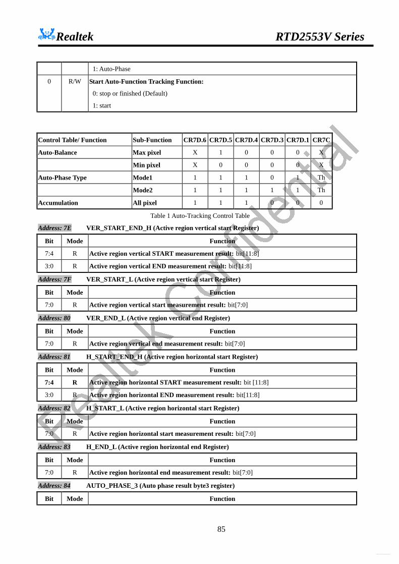
Realtek RTD2553V Series
85
1: Auto-Phase
0 R/W Start Auto-Function Tracking Function:
0: stop or finished (Default)
1: start
Control Table/ Function Sub-Function CR7D.6 CR7D.5 CR7D.4 CR7D.3 CR7D.1 CR7C
Auto-Balance Max pixel X 1 0 0 0 X
Min pixel X 0 0 0 0 X
Auto-Phase Type Mode1 1 1 1 0 1 Th
Mode2 1 1 1 1 1 Th
Accumulation All pixel 1 1 1 0 0 0
Table 1 Auto-Tracking Control Table
Address: 7E VER_START_END_H (Active region vertical start Register)
Bit Mode Function
7:4 R Active region vertical START measurement result: bit[11:8]
3:0 R Active region vertical END measurement result: bit[11:8]
Address: 7F VER_START_L (Active region vertical start Register)
Bit Mode Function
7:0 R Active region vertical start measurement result: bit[7:0]
Address: 80 VER_END_L (Active region vertical end Register)
Bit Mode Function
7:0 R Active region vertical end measurement result: bit[7:0]
Address: 81 H_START_END_H (Active region horizontal start Register)
Bit Mode Function
7:4 R Active region horizontal START measurement result: bit [11:8]
3:0 R Active region horizontal END measurement result: bit[11:8]
Address: 82 H_START_L (Active region horizontal start Register)
Bit Mode Function
7:0 R Active region horizontal start measurement result: bit[7:0]
Address: 83 H_END_L (Active region horizontal end Register)
Bit Mode Function
7:0 R Active region horizontal end measurement result: bit[7:0]
Address: 84 AUTO_PHASE_3 (Auto phase result byte3 register)
Bit Mode Function
http://www.DataSheet4U.net/
datasheet pdf - http://www.DataSheet4U.net/
Realtek RTD2553V Series
86
7:0 R Auto phase measurement result: bit[31:24]
Address: 85 AUTO_PHASE_2 (Auto phase result byte2 register)
Bit Mode Function
7:0 R Auto phase measurement result: bit[23:16]
Address: 86 AUTO_PHASE_1 (Auto phase result byte1 register)
Bit Mode Function
7:0 R Auto phase measurement result: bit[15:8]
Address: 87 AUTO_PHASE_0 (Auto phase result byte0 register)
Bit Mode Function
7:0 R Auto phase measurement result: bit[7:0]
The measured value of R or G or B color max or min. (Auto-Balance)
Address: 88 Reserved to 0
Video (Color Space Conversion) Address: 89 YUV2RGB_CTRL (YUV to RGB Control Register) Default: 00h
Bit Mode Function
7:5 R/W YUV Coefficient Write Enable:
000: h12 high byte
001: h12 low byte
010: h22 high byte
011: h22 low byte
100: h23 high byte
101: h23 low byte
110: h33 high byte
111: h33 low byte
4 -- Reserved to 0
3 R/W Enable YUV/RGB coefficient Access:
0: Disable
1: Enable
If this bit is set, the address of the data port will reset to original, and continuously writes 6 bytes
2 R/W Cb Cr Clamp
0: Bypass
1: Cb-128, Cr-128
1 R/W Y Gain/Offset:
0 : Bypass
1: (Y-16)*1.164
http://www.DataSheet4U.net/
datasheet pdf - http://www.DataSheet4U.net/
Realtek RTD2553V Series
87
0 R/W Enable YUV to RGB Conversion:
0: Disable YUV-to-RGB conversion (Default)
1: Enable YUV-to-RGB conversion
Address: 8A YUV_RGB_COEF_DATA
Bit Mode Function
7:0 W COEF_DATA[7:0]
YUV/RGB matrix
−−
−
−−=
128128
)(16
330)1(164.12322)1(164.1
012)1(164.1
CbCr
orYY
horhhor
hor
BGR
l h12: 11 bits, 1 bit integer and 10-bit fractional bits (Default: 5_80h) l h22: 10 bits, all fractional bits (Default: 1_40h) l h23: 9 bits, the MSB mean 0.25 (Default: 0_A0h) l h33: 12 bits, 2 bit integer and 10-bit fractional bits (Default: 7_00h) l To fill ‘h’ coefficients expressed by 2’s complement without signed bit. l h22 and h23 can’t be 000h
http://www.DataSheet4U.net/
datasheet pdf - http://www.DataSheet4U.net/
Realtek RTD2553V Series
88
Embedded Timing Controller Address: 8B TCON_ADDR _PORT Default: 00h
Bit Mode Function
7:0 R/W Address port for embedded TCON access
Address: 8C TCON_DATA _PORT Default: 00h
Bit Mode Function
7:0 R/W Data port for embedded TCON access
Address: 8C-00 TC_CTRL1 (Timing Controller control register1) Default: 01h
Bit Mode Function
7 R/W Enable Timing Controller Function (Global)
0: Disable (Default)
1: Enable
Reset all TCON pins after Enable TCON function is set and ties low.
6 R/W TCON [n] Toggle Function Reset
0: Not reset (Default)
1: reset by DVS
5 R/W Inactive Period Data Controlled by internal TCON [13]
0: DEN (Default)
1: TCON [13]
4 R/W TCON_HS compensation
0: Real TCON_HS = TCON_HS-4, Real TCON_HS = TCON_HS-4
1: Real TCON_HS = TCON_HS-27, Real TCON_HS = TCON_HS-27
If setting TCON_HS > DH_Total, then setting TCON_HS must subtract DH_Total.
3 R/W Reserved to 0
2 R/W 6/8 bit RSDS
0: 6-bit RSDS panel
1: 8-bit RSDS panel
1:0 R/W Display Port Configuration:
00: TTL
01: HZ (pin 61~82, 85~106)
10: LVDS
11: RSDS
Address: 8C-01 LVDS Location Pin Driving Control Default: 08h
Bit Mode Function
7 R/W 2 line Sum of Difference Threshold 1 Value: bit [8], ie:TH1 (also refer to CR8C-03)
http://www.DataSheet4U.net/
datasheet pdf - http://www.DataSheet4U.net/
Realtek RTD2553V Series
89
6 R/W 2 line Sum of Difference Threshold 2 Value: bit [8], ie:TH2 (also refer to CR8C-04)
5 R/W Reserved to 0
4 R/W Pin 41/42/43/44/45/48/49/50/51/110/113/114/115/118/119/120/121/122 drive current setting
0: 4mA
1: 6mA
3:2 R/W Display Port Driving Current Control (RSDS / LVDS)
Pin 52~57, 61~70, 73~82, 85~94, 97~106, 111~112
00: 2.5mA
01: 3mA
10: 3.5mA
11: 4mA
1 R/W Display Port Driving Current Control (TTL)
Pin 52~57, 61~70, 73~82, 85~94, 97~106, 111~112
0: 4mA
1: 6mA
0 R/W Reserved to 0
Address: 8C-02 RSDS Misc Default: 00h
Bit Mode Function
7 R/W RSDS data latch Inverted
0: Non-Inverted
1: Inverted
6:4 R/W RSDS data latch Delay
000: 0ns delay
001: 0.5ns delay
010: 1ns delay
011: 1.5ns delay
100: 2ns delay
101: 2.5ns delay
110: 3ns delay
111: 3.5ns delay
3 R/W Reserved to 0
2 R/W RSDS Green / Clock Pair Swap (Also refer to CR29[6:4])
0: No Swap (Default)
1: Swap
1 R/W RSDS High/Low Bit Swap (data) (Also refer to CR29[6:4])
0: Swap (Default)
http://www.DataSheet4U.net/
datasheet pdf - http://www.DataSheet4U.net/
Realtek RTD2553V Series
90
1: No Swap
0 R/W RSDS Differential pair PN swap (data) (Also refer to CR29[6:4])
0: No Swap (Default)
1: Swap
AU 17" RSDS panel pin order:
B0B1B2G0G1G2CLKR0R1R2 QDI 17" RSDS panel pin order: B2B1B0G2G1G0CLKR2R1R0 CMO 17" RSDS panel pin order: B2B1B0CLKG2G1G0R2R1R0 l Total swap function:
Ø Even/Odd swap Ø Red/Blue swap Ø 8 bit MSB/LSB swap Ø 6 bit MSB/LSB swap Ø RSDS High/Low bit swap Ø RSDS P/N swap Ø RSDS Green/Clk swap
l 6 bit MSB/LSB swap è G1 G2 G3 CK à G3 G2 G1 CK l Green/Clk swap è G1 G2 G3 CK à CK G1 G2 G3 l 6 bit MSB/LSB swap first, then Green/Clk swap è G1 G2 G3 CK à G3 G2 G1 CK à CK G3 G2 G1 l 8 bit MSB/LSB swap è G0 G1 G2 G3 CK à G3 G2 G1 G0 CK l Green/Clk swap è G0 G1 G2 G3 CK à CK G0 G1 G2 G3 l 8 bit MSB/LSB swap first, then Green/Clk swap è G0 G1 G2 G3 CK à G3 G2 G1 G0 CK à CK G3 G2 G1 G0 Address: 8C-03 Pixel Threshold High Value for Smart Polarity (TH1) Default: 00h
Bit Mode Function 7:0 R/W 2 line Sum of Difference Threshold 1 Value: bit [7:0], ie:TH1 (also refer to CR8C-01[7])
Address: 8C-04 Pixel Threshold Low Value for Smart Polarity (TH2) Default: 00h
Bit Mode Function
7:0 R/W 2 line Sum of Difference Threshold 2 Value: bit [7:0], ie:TH2 (also refer to CR8C-01[6])
Address: 8C-05 Line Threshold Value for Smart Polarity Default: 00h
Bit Mode Function
7 R/W Measure Dot Pattern over Threshold
1: Run.
Auto: always measure (Reference to CR05[5])
Manual: start to measure, clear after finish
0: Stop
6 R Dot Pattern Sum of Difference Measure Result
1: Over threshold
0: Under threshold
5 R/W Anti-Flicker Auto-Measure Control
http://www.DataSheet4U.net/
datasheet pdf - http://www.DataSheet4U.net/
Realtek RTD2553V Series
91
1: Auto
0: Manual
4:0 R/W Over Difference Line Threshold Value: bit [4:0]
RSDS Display Data Bus Control Address: 8C-06 RSDS Display Data Bus Interleaving Line Buffer Length High Byte Default: 00h
Bit Mode Function
7 R/W RSDS Type III Line Buffer BIST Enable
0: Disable
1: Enable
6:5 R/W Buffer SRAM Selection
00: Front Even-SRAM
01: Front Odd-SRAM
10: Back Even-SRAM
11: Back Odd-SRAM
4 R/W BIST Test is running
0: Stop
1: Start
3 R/W BIST Test result
0: Fail
1: Ok
2 R/W Display Data Bus Interleaving Enable
0: Disable (Default)
1: Enable
1:0 R/W Interleaving Line Buffer Line Buffer: High Byte [9:8] Address: 8C-07 RSDS Display Data Bus Interleaving Line Buffer Length Low Byte Default: 00h
Bit Mode Function 7:0 R/W Interleaving Line Buffer Line Buffer: Low Byte [7:0]
TCON Horizontal/Vertical Timing Setting Address: 8C-08 TCON [0]_VS_LSB (TCON [0] Vertical Start LSB Register)
Bit Mode Function
7:0 W Line number [7:0] at which TCON control generation begins
Address: 8C-09 TCON [0]_VS_MSB (TCON [0] Vertical Start/End MSB Register)
Bit Mode Function
7:4 W Line number [11:8] at which TCON control generation ends
http://www.DataSheet4U.net/
datasheet pdf - http://www.DataSheet4U.net/
Realtek RTD2553V Series
92
3:0 W Line number [11:8] at which TCON control generation begins
Address: 8C-0A TCON [0]_VE_LSB (TCON [0] Vertical End LSB Register)
Bit Mode Function
7:0 W Line number [7:0] at which TCON control generation ends
Address: 8C-0B TCON [0]_HS_LSB (TCON [0] Horizontal Start LSB Register)
Bit Mode Function
7:0 W Pixel count [7:0] at which TCON goes active
Address: 8C-0C TCON [0]_HS_MSB (TCON [0] Horizontal Start/End MSB Register)
Bit Mode Function
7:4 W Pixel count [11:8] at which TCON goes inactive
3:0 W Pixel count [11:8] at which TCON goes active
To be triggered on rising edge of the DCLK
Address: 8C-0D TCON [0]_HE_LSB (TCON [0] Horizontal End LSB Register)
Bit Mode Function
7:0 W Pixel count [7:0] at which TCON goes inactive
If the register number is large than display format, the horizontal component is always on.
Real TCON_HS = TCON_HS-4, Real TCON_HS = TCON_HS-4
Address: 8C-0E TCON [0]_CTRL (TCON [0] Control Register) Default: 00h
Bit Mode Function
7 R/W TCON [n] Enable (Local)
0: Disable (TCON [n] output clamp to ‘0’) (Default)
1: Enable
6 R/W Polarity Control
0: Normal output (Default)
1: Inverted output
5:4 -- Reserved to 0
3 R/W Toggle Circuit Enable/Disable
0: Normal TCON output (Default)
1: Toggle Circuit enable
When using toggle circuit enable mode, the TCON[n] will be 1 clock earlier than TCON[n-1] and
then toggling together, finally output will be 1 clock delay comparing to toggling result.
2:0 R/W TCON [13:10] & TCON [7:4] (TCON Combination Select)
TCON [13] has inactive data controller function.
TCON [13]~[10] has dot masking function
TCON [7] has flicking reduce function.
000: Normal TCON output (Default)
http://www.DataSheet4U.net/
datasheet pdf - http://www.DataSheet4U.net/
Realtek RTD2553V Series
93
001: Select TCON [n] “AND” with TCON [n-1]
010: Select TCON [n] “OR” with TCON [n-1]
011: Select TCON [n] “XOR” with TCON [n-1]
100: Select TCON [n-1] rising edge as toggle trigger signal (when toggle enable)
101: Select TCON [n-1] rising edge as toggle trigger signal, then “AND” (when toggle enable)
110: Select TCON [n-1] rising edge as toggle trigger signal, then “OR” (when toggle enable)
111: Select TCON [n] and TCON [n-1] on alternating frames.
--------------------------------------------------------------------------------------------------------------------
TCON [9:8] (TCON Combination Select)
000: Normal TCON output
001: Select TCON [n] “AND” with TCON [n-1]
010: Select TCON [n] “OR” with TCON [n-1]
011: Select TCON [n] “XOR” with TCON [n-1]
100: Select TCON [n-1] rising edge as toggle trigger signal (when toggle enable)
101: Select TCON [n-1] rising edge as toggle trigger signal, then “AND” (when toggle enable)
110: Select TCON [n-1] rising edge as toggle trigger signal, then “OR” (when toggle enable)
111: Select TCON [n] and TCON [n-1] reference ODD signal as alternating frames.
--------------------------------------------------------------------------------------------------------------------
TCON [3] (TCON Combination Select)
000: Normal TCON output
001: Select TCON [3] “AND” with TCON [2]
010: Select TCON [3] “OR” with TCON [2]
011: Select TCON [3] “XOR” with TCON [2]
100: Select TCON [2] rising edge as toggle trigger signal (when toggle enable)
101: Select TCON [2] rising edge as toggle trigger signal, then “AND” (when toggle enable)
110: Select TCON [2] rising edge as toggle trigger signal, then “OR” (when toggle enable)
111: Select reset(ODD=0) or set(ODD=1) TCON [3] by DVS, when toggle function enable
--------------------------------------------------------------------------------------------------------------------
TCON [2] (Clock Toggle Function)//toggle function is inactive
00x: Normal TCON output
010: Select DCLK/2 when TCON [2] is “0”
011: Select DCLK/2 when TCON [2] is “1”
100: Select DCLK/4 when TCON [2] is “0”
101: Select DCLK/4 when TCON [2] is “1”
110: Select DCLK/8 when TCON [2] is “0”
111: Select DCLK/8 when TCON [2] is “1”
--------------------------------------------------------------------------------------------------------------------
http://www.DataSheet4U.net/
datasheet pdf - http://www.DataSheet4U.net/

Realtek RTD2553V Series
94
TCON [1]
xx0: Normal TCON output
xx1: Reverse-Control Signal output
--------------------------------------------------------------------------------------------------------------------
TCON [0]
00x: Normal TCON output
010: EVEN “REV” 18/24-bit function (“REV0” on TCON [0])
ODD “REV” 18/24-bit function (“REV1” on TCON [1])
011: ALL “REV” 36/48-bit function (“REV” on TCON [0], can also on TCON [1])
100: EVEN data Output Inversion Controlled by TCON [0] is “0”
ODD data Output Inversion Controlled by TCON [1] is “0”
101: EVEN data Output Inversion Controlled by TCON [0] is “1”
ODD data Output Inversion Controlled by TCON [1] is “1”
Dot masking Address: 8C-5F/67/6F/77 TC_DOT_MASKING_CTRL Default: 00h
Bit Mode Function
7:3 R/W Reserved to 0
2 R/W Red Dot Masking Enable
0: Disable (Default)
1: Enable
1 R/W Green Dot Masking Enable
0: Disable (Default)
1: Enable
0 R/W Blue Dot Masking Enable
0: Disable (Default)
1: Enable
When applying dot masking, the timing setting for TCON will be
Real TCON_Mask_STA = TCON_STA+2
Real TCON_Mask_END = TCON_END +2
TCON [0] ~ TCON [13] Control Registers Address Map
Address Data(# bits) Default
0A,09,08 TCON [0]_VS_REG (11)
0D,0C,0B TCON [0]_HS_REG (11)
0E TCON [0]_CTRL_REG 00
http://www.DataSheet4U.net/
datasheet pdf - http://www.DataSheet4U.net/
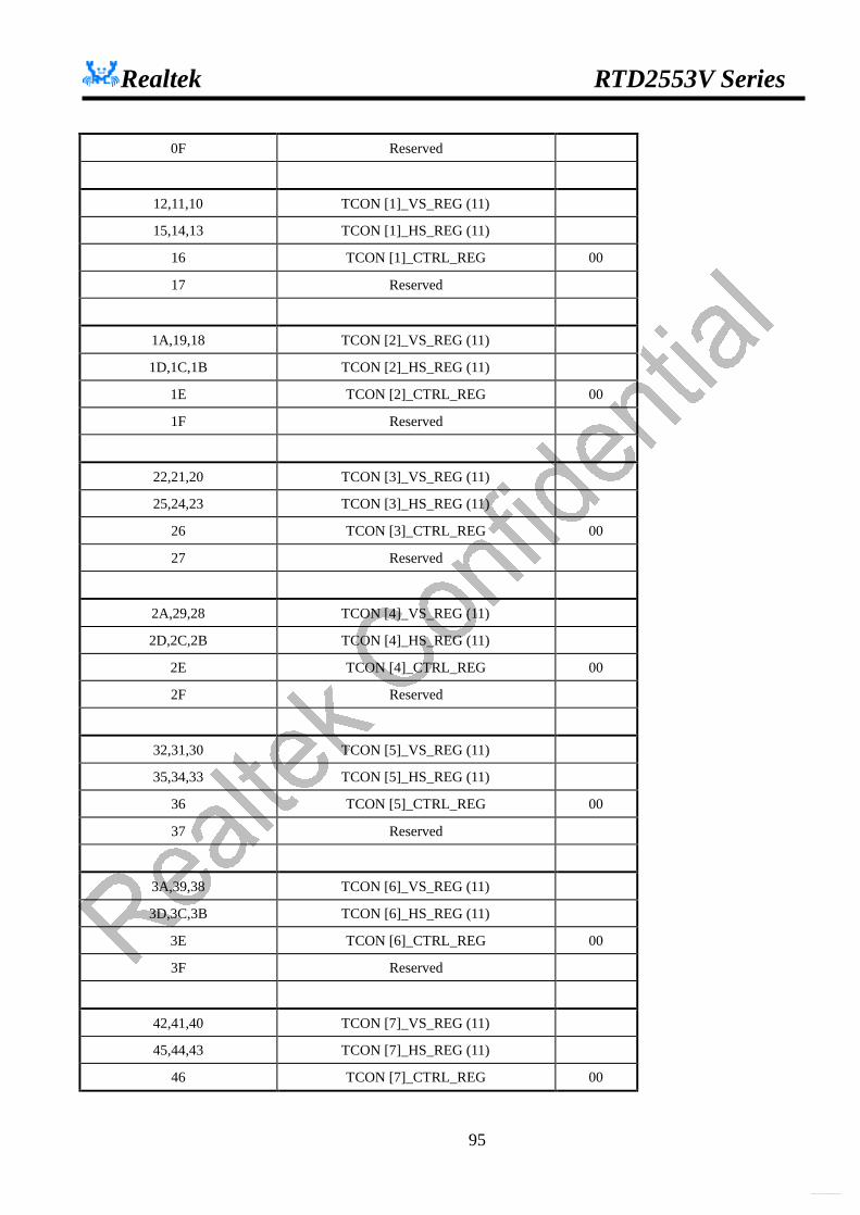
Realtek RTD2553V Series
95
0F Reserved
12,11,10 TCON [1]_VS_REG (11)
15,14,13 TCON [1]_HS_REG (11)
16 TCON [1]_CTRL_REG 00
17 Reserved
1A,19,18 TCON [2]_VS_REG (11)
1D,1C,1B TCON [2]_HS_REG (11)
1E TCON [2]_CTRL_REG 00
1F Reserved
22,21,20 TCON [3]_VS_REG (11)
25,24,23 TCON [3]_HS_REG (11)
26 TCON [3]_CTRL_REG 00
27 Reserved
2A,29,28 TCON [4]_VS_REG (11)
2D,2C,2B TCON [4]_HS_REG (11)
2E TCON [4]_CTRL_REG 00
2F Reserved
32,31,30 TCON [5]_VS_REG (11)
35,34,33 TCON [5]_HS_REG (11)
36 TCON [5]_CTRL_REG 00
37 Reserved
3A,39,38 TCON [6]_VS_REG (11)
3D,3C,3B TCON [6]_HS_REG (11)
3E TCON [6]_CTRL_REG 00
3F Reserved
42,41,40 TCON [7]_VS_REG (11)
45,44,43 TCON [7]_HS_REG (11)
46 TCON [7]_CTRL_REG 00
http://www.DataSheet4U.net/
datasheet pdf - http://www.DataSheet4U.net/
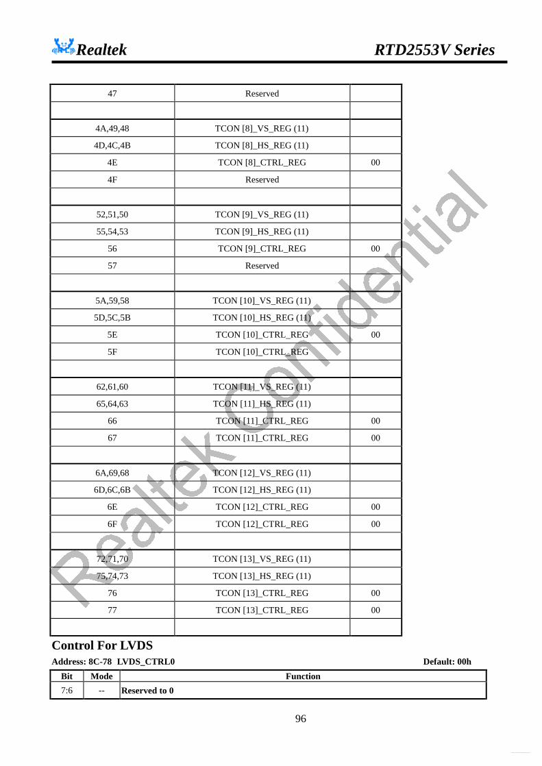
Realtek RTD2553V Series
96
47 Reserved
4A,49,48 TCON [8]_VS_REG (11)
4D,4C,4B TCON [8]_HS_REG (11)
4E TCON [8]_CTRL_REG 00
4F Reserved
52,51,50 TCON [9]_VS_REG (11)
55,54,53 TCON [9]_HS_REG (11)
56 TCON [9]_CTRL_REG 00
57 Reserved
5A,59,58 TCON [10]_VS_REG (11)
5D,5C,5B TCON [10]_HS_REG (11)
5E TCON [10]_CTRL_REG 00
5F TCON [10]_CTRL_REG
62,61,60 TCON [11]_VS_REG (11)
65,64,63 TCON [11]_HS_REG (11)
66 TCON [11]_CTRL_REG 00
67 TCON [11]_CTRL_REG 00
6A,69,68 TCON [12]_VS_REG (11)
6D,6C,6B TCON [12]_HS_REG (11)
6E TCON [12]_CTRL_REG 00
6F TCON [12]_CTRL_REG 00
72,71,70 TCON [13]_VS_REG (11)
75,74,73 TCON [13]_HS_REG (11)
76 TCON [13]_CTRL_REG 00
77 TCON [13]_CTRL_REG 00
Control For LVDS Address: 8C-78 LVDS_CTRL0 Default: 00h
Bit Mode Function 7:6 -- Reserved to 0
http://www.DataSheet4U.net/
datasheet pdf - http://www.DataSheet4U.net/

Realtek RTD2553V Series
97
5 R/W Power up LVDS even-port
0: Power down (Default)
1: Normal 4 R/W Power up LVDS odd-port
0: Power down (Default)
1: Normal 3:2 R/W Watch Dog Model
00: Enable Watch Dog(Default)
01: Keep PLL VCO = 1V
1x: Disable Watch Dog 1 Reversed 0 R Watch Dog Control Flag
0: Watch dog not active (Default)
1: Watch dog active, Reset PLL and set VCO = 1V
Address: 8C-79 LVDS_CTRL1 Default: 14h Bit Mode Function 7:6 R/W Reserved to 0 5:3 R/W STSTL [2:0]: select test attribute
000: WD
001: VCOM
010: IB40u (default)
011: IBVOCM
100: PLLTST-fbak
101: PLLTST-fin
110: LVTST-CKDIN
111: LVTST-LVDSIN[6] 2:0 R/W RSDS / LVDS Output Common Mode (Default: 100)
Address: 8C-7A LVDS_CTRL2 Default: 03h Bit Mode Function 7:6 -- Reserved to 0 5:4 -- Reserved 3 R/W PLL lock edge
0: positive
1: negative 2:0 R/W Bias Generator Adjust (011)
Address: 8C-7B LVDS_CTRL3 Default: 1Ch
Bit Mode Function
http://www.DataSheet4U.net/
datasheet pdf - http://www.DataSheet4U.net/

Realtek RTD2553V Series
98
7 R/W Reserved to 0
6 R/W LVDS mirror (Pin 73~82, 85~94)
0: Normal (TXE3+, TXE3-, TXEC+, TXEC-, TXE2+, TXE2-, TXE1+, TXE1-, TXE0+, TXE0-,
TXO3+, TXO3-, TXOC+, TXOC-, TXO2+, TXO2-, TXO1+, TXO1-, TXO0+, TXO0-)
1: Mirror (TXO0+, TXO0-, TXO1+, TXO1-, TXO2+, TXO2-, TXOC+, TXOC-, TXO3+, TXO3-,
TXE0+, TXE0-, TXE1+, TXE1-, TXE2+, TXE2-, TXEC+, TXEC-, TXE3+, TXE3-) 5:3 R/W SIL [2:0]: PLL charge pump current (I=5uA+5uA*code) (Default: 011) 2:1 R/W SRL [1:0]: PLL resistor (R=6K+2K*code) (Default: 10) 0 R/W BMTS: Bit-Mapping Table Select
0: Table 1 (Default)
1: Table 2
TCLK+ LVDS Bit 1 Bit 0 Bit 6 Bit 5 Bit 4 Bit 3 Bit 2 Bit 1 Bit 0 Bit 6 Bit 5 TXE0 ER1 ER0 EG0 ER5 ER4 ER3 ER2 ER1 ER0 EG0 ER5 TXE1 EG2 EG1 EB1 EB0 EG5 EG4 EG3 EG2 EG1 EB1 EB0 TXE2 EB3 EB2 DEN VS HS EB5 EB4 EB3 EB2 DEN*6 VS*5 TXE3 ER7 ER6 RSV EB7 EB6 EG7 EG6 ER7 ER6 RSV*7 EB7 TXO0 OR1 OR0 OG0 OR5 OR4 OR3 OR2 OR1 OR0 OG0 OR5 TXO1 OG2 OG1 OB1 OB0 OG5 OG4 OG3 OG2 OG1 OB1 OB0 TXO2 OB3 OB2 DEN VS HS OB5 OB4 OB3 OB2 DEN*2 VS*1 TXO3 OR7 OR6 RSV OB7 OB6 OG7 OG6 OR7 OR6 RSV*3 OB7
TABLE 1 Bit-Mapping 6bit(5~0)+2bit(7~6) TCLK+ LVDS Bit 1 Bit 0 Bit 6 Bit 5 Bit 4 Bit 3 Bit 2 Bit 1 Bit 0 Bit 6 Bit 5 TXE0 ER3 ER2 EG2 ER7 ER6 ER5 ER4 ER3 ER2 EG2 ER7 TXE1 EG4 EG3 EB3 EB2 EG7 EG6 EG5 EG4 EG3 EB3 EB2 TXE2 EB5 EB4 DEN VS HS EB7 EB6 EB5 EB4 DEN*6 VS*5 TXE3 ER1 ER0 RSV EB1 EB0 EG1 EG0 ER1 ER0 RSV*7 EB1 TXO0 OR3 OR2 OG2 OR7 OR6 OR5 OR4 OR3 OR2 OG2 OR7 TXO1 OG4 OG3 OB3 OB2 OG7 OG6 OG5 OG4 OG3 OB3 OB2 TXO2 OB5 OB4 DEN VS HS OB7 OB6 OB5 OB4 DEN*2 VS*1 TXO3 OR1 OR0 RSV OB1 OB0 OG1 OG0 OR1 OR0 RSV*3 OB1
TABLE 2 Bit-Mapping 6bit(7~2)+2bit(1~0) Address: 8C-7C LVDS_CTRL4 Default: 80h
Bit Mode Function 7:6 R/W E_RSV: even port reserve signal select
11: Always ‘1’
10: Always ‘0’
01: TCON [11]
00: PWM_0
http://www.DataSheet4U.net/
datasheet pdf - http://www.DataSheet4U.net/
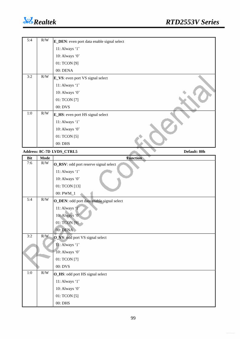
Realtek RTD2553V Series
99
5:4 R/W E_DEN: even port data enable signal select
11: Always ‘1’
10: Always ‘0’
01: TCON [9]
00: DENA 3:2 R/W E_VS: even port VS signal select
11: Always ‘1’
10: Always ‘0’
01: TCON [7]
00: DVS 1:0 R/W E_HS: even port HS signal select
11: Always ‘1’
10: Always ‘0’
01: TCON [5]
00: DHS
Address: 8C-7D LVDS_CTRL5 Default: 80h Bit Mode Function 7:6 R/W O_RSV: odd port reserve signal select
11: Always ‘1’
10: Always ‘0’
01: TCON [13]
00: PWM_1 5:4 R/W O_DEN: odd port data enable signal select
11: Always ‘1’
10: Always ‘0’
01: TCON [9]
00: DENA 3:2 R/W O_VS: odd port VS signal select
11: Always ‘1’
10: Always ‘0’
01: TCON [7]
00: DVS 1:0 R/W O_HS: odd port HS signal select
11: Always ‘1’
10: Always ‘0’
01: TCON [5]
00: DHS
http://www.DataSheet4U.net/
datasheet pdf - http://www.DataSheet4U.net/
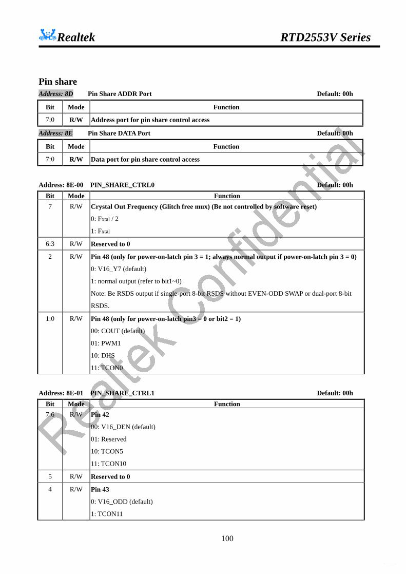
Realtek RTD2553V Series
100
Pin share Address: 8D Pin Share ADDR Port Default: 00h
Bit Mode Function
7:0 R/W Address port for pin share control access
Address: 8E Pin Share DATA Port Default: 00h
Bit Mode Function
7:0 R/W Data port for pin share control access
Address: 8E-00 PIN_SHARE_CTRL0 Default: 00h
Bit Mode Function 7 R/W Crystal Out Frequency (Glitch free mux) (Be not controlled by software reset)
0: Fxtal / 2
1: Fxtal
6:3 R/W Reserved to 0
2 R/W Pin 48 (only for power-on-latch pin 3 = 1; always normal output if power-on-latch pin 3 = 0)
0: V16_Y7 (default)
1: normal output (refer to bit1~0)
Note: Be RSDS output if single-port 8-bit RSDS without EVEN-ODD SWAP or dual-port 8-bit
RSDS.
1:0 R/W Pin 48 (only for power-on-latch pin3 = 0 or bit2 = 1)
00: COUT (default)
01: PWM1
10: DHS
11: TCON0
Address: 8E-01 PIN_SHARE_CTRL1 Default: 00h
Bit Mode Function 7:6 R/W Pin 42
00: V16_DEN (default)
01: Reserved
10: TCON5
11: TCON10
5 R/W Reserved to 0
4 R/W Pin 43
0: V16_ODD (default)
1: TCON11
http://www.DataSheet4U.net/
datasheet pdf - http://www.DataSheet4U.net/

Realtek RTD2553V Series
101
3:2 R/W Pin 44
00: V16_HS (default)
01: Reserved
10: TCON4
11: TCON8
1:0 R/W Pin 45
00: V16_VS (default)
01: Reserved
10: TCON3
11: TCON9
Address: 8E-02 PIN_SHARE_CTRL2 Default: 00h
Bit Mode Function
7:6 R/W Pin 3 (Power on latch for MCU location selection)
00: PWM0 (default)
01: TCON0
10: DVS
11: TCON3
5:4 R/W Pin 4
00: PWM1 (default)
01: TCON1
10: DHS
11: TCON12
3 R/W Pin 110
0: COUT (default)
1: TCON13
2:0 R/W Pin 111
000: V8_0 (default)
001: ARED1
010: PWM1
011: TCON2
100: TCON7
101: reserved
110: reserved
111: reserved
Note: Be RSDS output if single-port 8-bit RSDS with EVEN-ODD SWAP or dual-port 8-bit
RSDS.
http://www.DataSheet4U.net/
datasheet pdf - http://www.DataSheet4U.net/
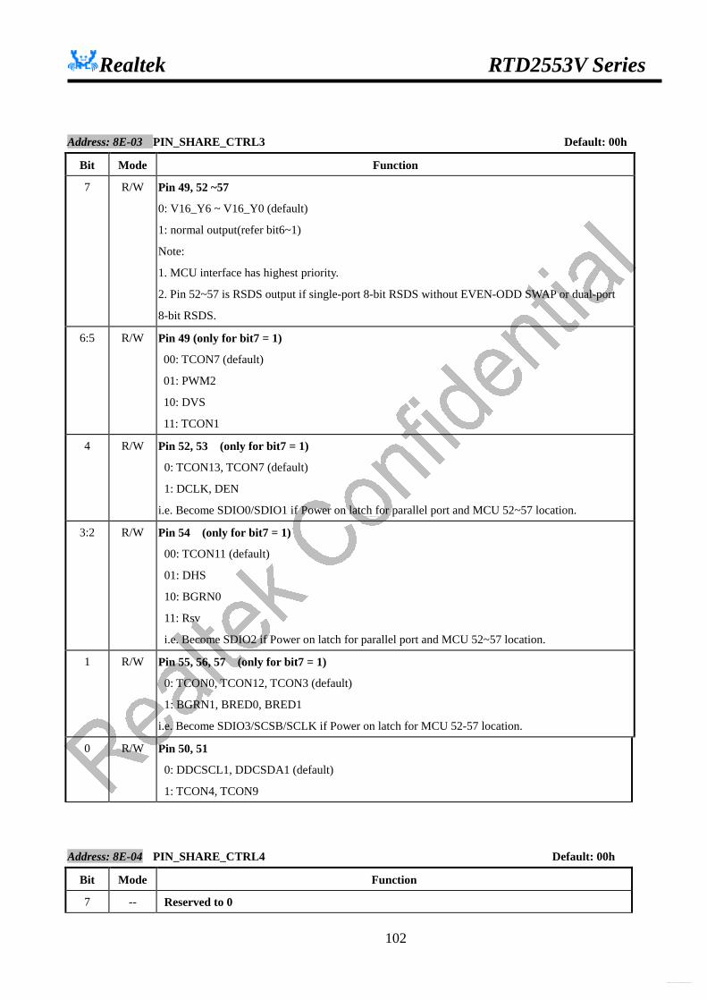
Realtek RTD2553V Series
102
Address: 8E-03 PIN_SHARE_CTRL3 Default: 00h
Bit Mode Function
7 R/W Pin 49, 52 ~57
0: V16_Y6 ~ V16_Y0 (default)
1: normal output(refer bit6~1)
Note:
1. MCU interface has highest priority.
2. Pin 52~57 is RSDS output if single-port 8-bit RSDS without EVEN-ODD SWAP or dual-port
8-bit RSDS.
6:5 R/W Pin 49 (only for bit7 = 1)
00: TCON7 (default)
01: PWM2
10: DVS
11: TCON1
4 R/W Pin 52, 53 (only for bit7 = 1)
0: TCON13, TCON7 (default)
1: DCLK, DEN
i.e. Become SDIO0/SDIO1 if Power on latch for parallel port and MCU 52~57 location.
3:2 R/W Pin 54 (only for bit7 = 1)
00: TCON11 (default)
01: DHS
10: BGRN0
11: Rsv
i.e. Become SDIO2 if Power on latch for parallel port and MCU 52~57 location.
1 R/W Pin 55, 56, 57 (only for bit7 = 1)
0: TCON0, TCON12, TCON3 (default)
1: BGRN1, BRED0, BRED1
i.e. Become SDIO3/SCSB/SCLK if Power on latch for MCU 52-57 location.
0 R/W Pin 50, 51
0: DDCSCL1, DDCSDA1 (default)
1: TCON4, TCON9
Address: 8E-04 PIN_SHARE_CTRL4 Default: 00h
Bit Mode Function
7 -- Reserved to 0
http://www.DataSheet4U.net/
datasheet pdf - http://www.DataSheet4U.net/

Realtek RTD2553V Series
103
6 R/W Pin 122
0: PWM0 (default)
1: TCON9
5:4 R/W Pin 112, 113, 114
00: V8_1, V8_2, V8_3 (default)
01: ARED0, AGRN1, AGRN0
10: PWM2, DDCSCL2, DDCSDA2
11: TCON10, TCON8, TCON5
Note
1. Become SDIO0/SDIO1/SDIO2 if Power on latch for parallel port and MCU 112~119 location.
2. Pin 112 is RSDS output if single-port 8-bit RSDS with EVEN-ODD SWAP or dual-port 8-bit
RSDS.
3 R/W Pin 115, 118, 119
0: V8_4, V8_5, V8_6 (default)
1: TCON9, TCON7, TCON3
i.e. Become SDIO3/SCSB/SCLK if Power on latch for MCU 112~119 location.
2:0 R/W Pin 120, 121
000: V8_7, VCLK (default)
001: DCLK, DENA
010: DDCSDA2, DDCSCL2
011: TCON6, TCON4
100: TCON11, TCON4
101: reserved
110: reserved
111: reserved
http://www.DataSheet4U.net/
datasheet pdf - http://www.DataSheet4U.net/
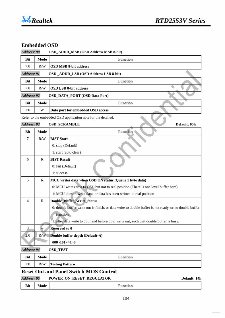
Realtek RTD2553V Series
104
Embedded OSD Address: 90 OSD_ADDR_MSB (OSD Address MSB 8-bit)
Bit Mode Function
7:0 R/W OSD MSB 8-bit address
Address: 91 OSD _ADDR_LSB (OSD Address LSB 8-bit)
Bit Mode Function
7:0 R/W OSD LSB 8-bit address
Address: 92 OSD_DATA_PORT (OSD Data Port)
Bit Mode Function
7:0 W Data port for embedded OSD access
Refer to the embedded OSD application note for the detailed.
Address: 93 OSD_SCRAMBLE Default: 05h
Bit Mode Function
7 R/W BIST Start
0: stop (Default)
1: start (auto clear)
6 R BIST Result
0: fail (Default)
1: success
5 R MCU writes data when OSD ON status (Queue 1 byte data)
0: MCU writes data to OSD but not to real position (There is one level buffer here)
1: MCU doesn’t write data, or data has been written to real position
4 R Double_Buffer_Write_Status
0: double buffer write out is finish, or data write to double buffer is not ready, or no double buffer
function.
1: after data write to dbuf and before dbuf write out, such that double buffer is busy.
3 -- Reserved to 0
2:0 R/W Double buffer depth (Default=6)
000~101=>1~6
Address: 94 OSD_TEST
Bit Mode Function
7:0 R/W Testing Pattern
Reset Out and Panel Switch MOS Control Address: 95 POWER_ON_RESET_REGULATOR Default: 14h
Bit Mode Function
http://www.DataSheet4U.net/
datasheet pdf - http://www.DataSheet4U.net/
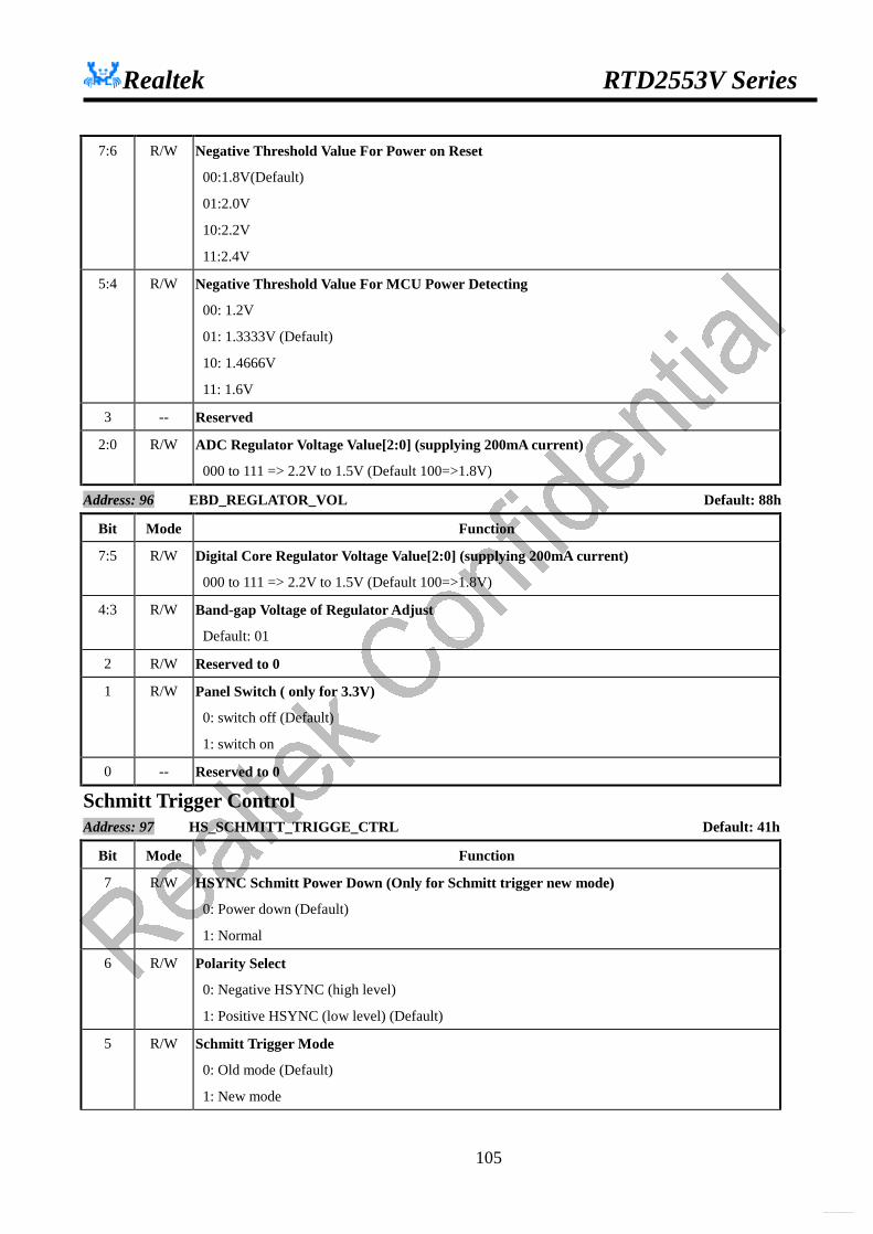
Realtek RTD2553V Series
105
7:6 R/W Negative Threshold Value For Power on Reset
00:1.8V(Default)
01:2.0V
10:2.2V
11:2.4V
5:4 R/W Negative Threshold Value For MCU Power Detecting
00: 1.2V
01: 1.3333V (Default)
10: 1.4666V
11: 1.6V
3 -- Reserved
2:0 R/W ADC Regulator Voltage Value[2:0] (supplying 200mA current)
000 to 111 => 2.2V to 1.5V (Default 100=>1.8V)
Address: 96 EBD_REGLATOR_VOL Default: 88h
Bit Mode Function
7:5 R/W Digital Core Regulator Voltage Value[2:0] (supplying 200mA current)
000 to 111 => 2.2V to 1.5V (Default 100=>1.8V)
4:3 R/W Band-gap Voltage of Regulator Adjust
Default: 01
2 R/W Reserved to 0
1 R/W Panel Switch ( only for 3.3V)
0: switch off (Default)
1: switch on
0 -- Reserved to 0
Schmitt Trigger Control Address: 97 HS_SCHMITT_TRIGGE_CTRL Default: 41h
Bit Mode Function
7 R/W HSYNC Schmitt Power Down (Only for Schmitt trigger new mode)
0: Power down (Default)
1: Normal
6 R/W Polarity Select
0: Negative HSYNC (high level)
1: Positive HSYNC (low level) (Default)
5 R/W Schmitt Trigger Mode
0: Old mode (Default)
1: New mode
http://www.DataSheet4U.net/
datasheet pdf - http://www.DataSheet4U.net/

Realtek RTD2553V Series
106
4 R/W Threshold Voltage Fine Tune (only for Schmitt trigger new mode)
0: 0V (Default)
1: -0.1V
3:2 R/W Positive Threshold Voltage
1:0 R/W Negative Threshold Voltage l There are 3 mode of the HSYNC Schmitt trigger.
1. Old mode 1: original HSYNC Schmitt trigger. bit[6:5]=00 è Vt
+ = 1.5V, Vt- = 1.0V
2. Old mode 2: The easy HSYNC Schmitt trigger. bit[6:5]=10 è Bit[1:0] Vt
+ Vt-
01 2.0V 1.5V 11 1.5V 1.0V
3. New mode: Fully programmable Schmitt trigger. The following table will determine the Schmitt Trigger positive and negative voltage: bit[6]=1 (Positive HSYNC) bit[6] = 0 (Negative HSYNC) bit[3:2] Vt
+ bit[1:0] Vt- bit[3:2] Vt
+ bit[1:0] Vt-
00 1.4V 00 Vt+ - 1.2V 00 1.8V 00 Vt
+ - 1.2V 01 1.6V 01 Vt
+ - 1.0V 01 2.0V 01 Vt+ - 1.0V
10 1.8V 10 Vt+ - 0.8V 10 2.2V 10 Vt
+ - 0.8V 11 2.0V 11 Vt
+ - 0.6V 11 2.4V 11 Vt+ - 0.6V
l After we get the threshold voltage by the table, we still can fine tune it: Final Positive Threshold Voltage = Vt
+ - 0.1* bit[4] Final Negative Threshold Voltage = Vt
-- 0.1* bit[4]
http://www.DataSheet4U.net/
datasheet pdf - http://www.DataSheet4U.net/

Realtek RTD2553V Series
107
Phase-Lock-Loop (PLL) DDS Setting for ADC Address: 98 PLL_DIV_CTRL Default: 04h
Bit Mode Function 7 R/W PFD Selection
0: New PFD fine (Default) 1: New PFD coarse ( the resolution will be 1/2 of the PFD fine mode)
6 R/W DDS Tracking Edge 0: HS positive edge (Default) 1: HS negative edge
5 R/W DDS Reset Enable 0: Normal function (Default) 1: DDS circuit’s reset will be asserted, for test only
4 R/W Test Mode: (for production test) 0: Normal (Default) 1: Test Mode
3 R/W HS output synchronized by 0: phase 32 1: phase 0 (Default)
2:1 R/W Delay Compensation Mode 00: Mode 0 01: Mode 1 10: Mode 2 (Default) 11: Mode 3
0 R/W Clock select for DIV 0: phase 0 (phase-0 of PLL2) (Default) 1: internal CLK (Fav)
Address: 99 I_CODE_L Default: 47h Bit Mode Function 7:3 R/W Old/New mode: I_Code [9:5] (Default: 01000) 2 R/W Old mode: I_Code [4] (Default=1)
New mode:
I-code control mechanism
0: new linear mode, PE*(2+NEW_I[13])
1: old mode, P-code = I[17:0] – 1 (Default) 1:0 R/W Old mode: I_Code [3:2] (Default: 11)
New mode: P-code protection mode
00 => No protection
01 => 1 bit protection
10 => 2 bits protection
11 => 3 bits protection (Default) Address: 9A I_CODE_M Default: 00h
Bit Mode Function 7:6 R/W Old mode :I_Code [15:14] (Default: 00) 5 R/W Old mode :I_code [13] (Default:0)
http://www.DataSheet4U.net/
datasheet pdf - http://www.DataSheet4U.net/

Realtek RTD2553V Series
108
New mode :I_code calibrated setting 4 R/W Old mode :I_Code [12] (Default:0)
New mode :P_code calibrated setting 3 R/W Old mode :I_Code [11] 2 R/W I_Code [10] or PFD type selection
0: Old PFD (Default)
1: New PFD 1 R/W Old mode :I_Code [1] (Default: 0)
New mode :
P-code mapping curve
0: choose the new P-code mapping curve (PE*2+NEW_I[12])* 2_2 +PNEW 1: choose the old P-code mapping curve
0 R/W Old mode: I_Code [0] (Default: 0)
New mode:
I-code multiplication factor
0: choose the new I-code multiplication factor = )2]5:9[_(2 +INEW 1: choose the old I-code multiplication factor
I CONTROL =( I-CODE control mechanism)*(I-code multiplication factor) Address: 9B P_CODE Default: 18h
Bit Mode Function 7 R/W Phase Swallow Down Enable
0: Swallow Up (Default) 1: Swallow Down
6:5 R/W I_Code[17:16] Default: 00b 4:0 R/W P_Code[4:0] Default: 18h
Address: 9C PFD_CALIBRATED_RESULTS Default: 8’b 00xxxxxx Bit Mode Function
7 -- Reserved to 0 6 R/W PFD Calibration Enable
Overwrite 0 to 1 return a new PFD calibrated value. 5:0 R PFD Calibrated Results[5:0]
Address: 9D PE_MEARSURE Default: 00h Bit Mode Function 7:6 -- Reserved to 0 5 R/W PE Measure Enable
0: Disable (Default)
1: Start PE Measurement, clear after finish. 4:0 R PE Value Result [4:0]
Address: 9E PE_MAX_MEASURE Default: 00h
http://www.DataSheet4U.net/
datasheet pdf - http://www.DataSheet4U.net/
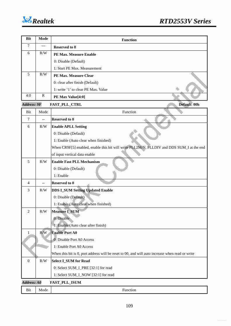
Realtek RTD2553V Series
109
Bit Mode Function 7 --- Reserved to 0 6 R/W PE Max. Measure Enable
0: Disable (Default)
1: Start PE Max. Measurement 5 R/W PE Max. Measure Clear
0: clear after finish (Default)
1: write ‘1’ to clear PE Max. Value 4:0 R PE Max Value[4:0]
Address: 9F FAST_PLL_CTRL Default: 00h
Bit Mode Function
7 -- Reserved to 0
6 R/W Enable APLL Setting
0: Disable (Default)
1: Enable (Auto clear when finished)
When CR9F[5] enabled, enable this bit will write PLL2M/N, PLLDIV and DDS SUM_I at the end
of input vertical data enable
5 R/W Enable Fast PLL Mechanism
0: Disable (Default)
1: Enable
4 -- Reserved to 0
3 R/W DDS I_SUM Setting Updated Enable
0: Disable (Default)
1: Enable (Auto clear when finished)
2 R/W Measure I_SUM
0: Disable
1: Enable (Auto clear after finish)
1 R/W Enable Port A0
0: Disable Port A0 Access
1: Enable Port A0 Access
When this bit is 0, port address will be reset to 00, and will auto increase when read or write
0 R/W Select I_SUM for Read
0: Select SUM_I_PRE [32:1] for read
1: Select SUM_I_NOW [32:1] for read
Address: A0 FAST_PLL_ISUM
Bit Mode Function
http://www.DataSheet4U.net/
datasheet pdf - http://www.DataSheet4U.net/
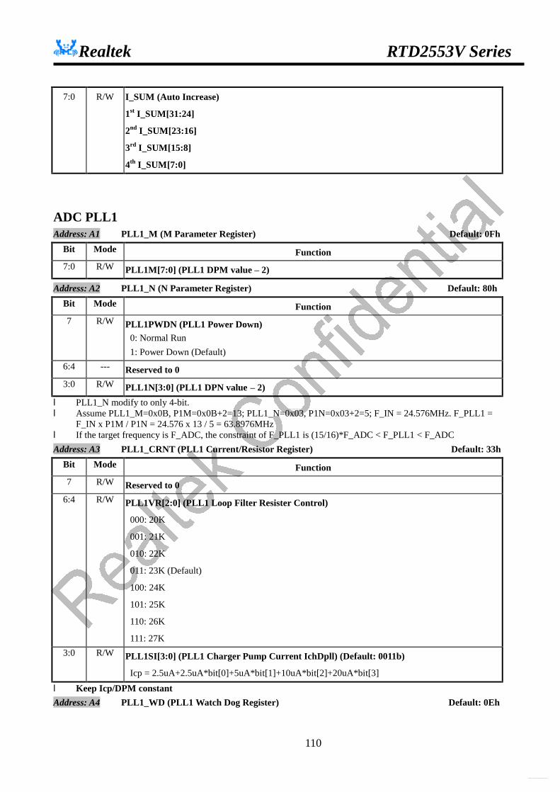
Realtek RTD2553V Series
110
7:0 R/W I_SUM (Auto Increase)
1st I_SUM[31:24]
2nd I_SUM[23:16]
3rd I_SUM[15:8]
4th I_SUM[7:0]
ADC PLL1 Address: A1 PLL1_M (M Parameter Register) Default: 0Fh
Bit Mode Function 7:0 R/W PLL1M[7:0] (PLL1 DPM value – 2)
Address: A2 PLL1_N (N Parameter Register) Default: 80h Bit Mode Function 7 R/W PLL1PWDN (PLL1 Power Down)
0: Normal Run 1: Power Down (Default)
6:4 --- Reserved to 0 3:0 R/W PLL1N[3:0] (PLL1 DPN value – 2)
l PLL1_N modify to only 4-bit. l Assume PLL1_M=0x0B, P1M=0x0B+2=13; PLL1_N=0x03, P1N=0x03+2=5; F_IN = 24.576MHz. F_PLL1 =
F_IN x P1M / P1N = 24.576 x 13 / 5 = 63.8976MHz l If the target frequency is F_ADC, the constraint of F_PLL1 is (15/16)*F_ADC < F_PLL1 < F_ADC Address: A3 PLL1_CRNT (PLL1 Current/Resistor Register) Default: 33h
Bit Mode Function 7 R/W Reserved to 0
6:4 R/W PLL1VR[2:0] (PLL1 Loop Filter Resister Control)
000: 20K
001: 21K
010: 22K
011: 23K (Default)
100: 24K
101: 25K
110: 26K
111: 27K 3:0 R/W PLL1SI[3:0] (PLL1 Charger Pump Current IchDpll) (Default: 0011b)
Icp = 2.5uA+2.5uA*bit[0]+5uA*bit[1]+10uA*bit[2]+20uA*bit[3] l Keep Icp/DPM constant Address: A4 PLL1_WD (PLL1 Watch Dog Register) Default: 0Eh
http://www.DataSheet4U.net/
datasheet pdf - http://www.DataSheet4U.net/

Realtek RTD2553V Series
111
Bit Mode Function 7 R PLL1STATUS (PLL1 WD Status)
0: Normal (Default)
1: Abnormal 6 R/W PLL1WDRST (PLL1 WD Reset)
0: Normal (Default)
1: Reset 5 R/W PLL1WDSET (PLL1 WD Set)
0: Normal (Default) 1: Set
4:3 R/W PLL1WDVSET[1:0] (PLL1 WD Voltage Set)
00: 2.46V
01: 1.92V(Default)
10: 1.36V
11: 1.00V 2 R/W PLL1UPDN (PLL1 Frequency Tuning Up/Down)
0: Freq Down
1: Freq Up (Default) 1 R/W PLL1MSBSTOP (PLL1 Frequency Tuning Enable)
0: Disable
1: Enable (Default) 0 --- Reserved to 0
ADC PLL2 Address: A5 PLL2_M (M Parameter Register) Default: 3Eh
Bit Mode Function 7:0 R/W PLL2_M[7:0] (PLL2 DPM value – 2) (Default 3E)
Address: A6 PLL2_N (N Parameter Register) Default: 3Dh Bit Mode Function 7:0 R/W PLL2_N[7:0] (PLL2 DPN value – 2) (Default 3D)
l Assume PLL2_M=0x0A, P2M=0x0A+2=12; PLL2_N=0x04, P2N=0x04+2=6; F_IN =65 MHz . l F_PLL2 = F_IN x P2M x 2 / P2N /2 = 65 x 12 x 2 / 6 / 2 = 130 MHz l the constraint of F_PLL2 is that P2N =(int)(F_IN / 10) Address: A7 PLL2_CRNT (PLL2 Current/Resistor Control) Default: 6Fh
Bit Mode Function
7:5 R/W PLL2VR[2:0] (PLL2 Loop Filter Resister Control)
000: 15K
001: 16K
http://www.DataSheet4U.net/
datasheet pdf - http://www.DataSheet4U.net/
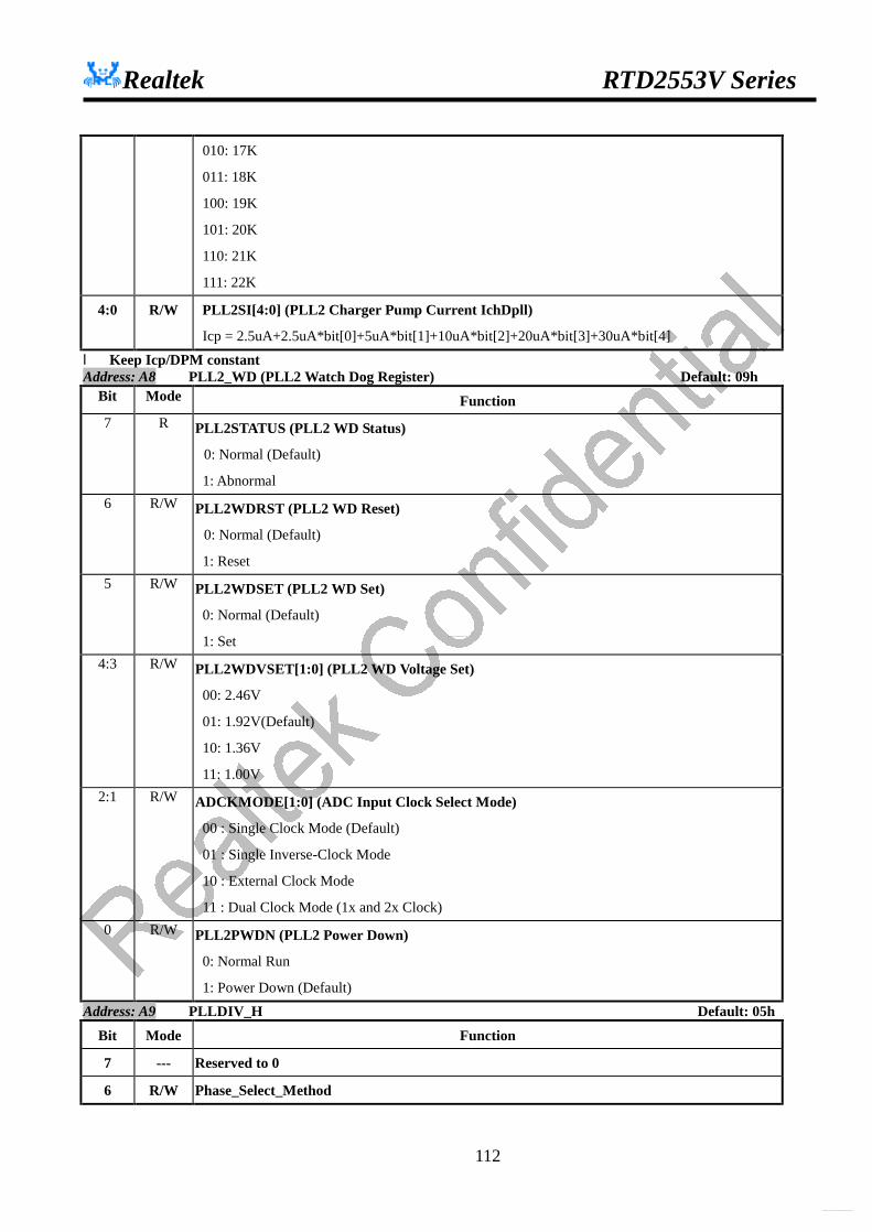
Realtek RTD2553V Series
112
010: 17K
011: 18K
100: 19K
101: 20K
110: 21K
111: 22K 4:0 R/W PLL2SI[4:0] (PLL2 Charger Pump Current IchDpll)
Icp = 2.5uA+2.5uA*bit[0]+5uA*bit[1]+10uA*bit[2]+20uA*bit[3]+30uA*bit[4] l Keep Icp/DPM constant Address: A8 PLL2_WD (PLL2 Watch Dog Register) Default: 09h
Bit Mode Function 7 R PLL2STATUS (PLL2 WD Status)
0: Normal (Default)
1: Abnormal 6 R/W PLL2WDRST (PLL2 WD Reset)
0: Normal (Default)
1: Reset 5 R/W PLL2WDSET (PLL2 WD Set)
0: Normal (Default)
1: Set 4:3 R/W PLL2WDVSET[1:0] (PLL2 WD Voltage Set)
00: 2.46V
01: 1.92V(Default)
10: 1.36V
11: 1.00V 2:1 R/W ADCKMODE[1:0] (ADC Input Clock Select Mode)
00 : Single Clock Mode (Default)
01 : Single Inverse-Clock Mode
10 : External Clock Mode
11 : Dual Clock Mode (1x and 2x Clock) 0 R/W PLL2PWDN (PLL2 Power Down)
0: Normal Run
1: Power Down (Default) Address: A9 PLLDIV_H Default: 05h
Bit Mode Function
7 --- Reserved to 0
6 R/W Phase_Select_Method
http://www.DataSheet4U.net/
datasheet pdf - http://www.DataSheet4U.net/
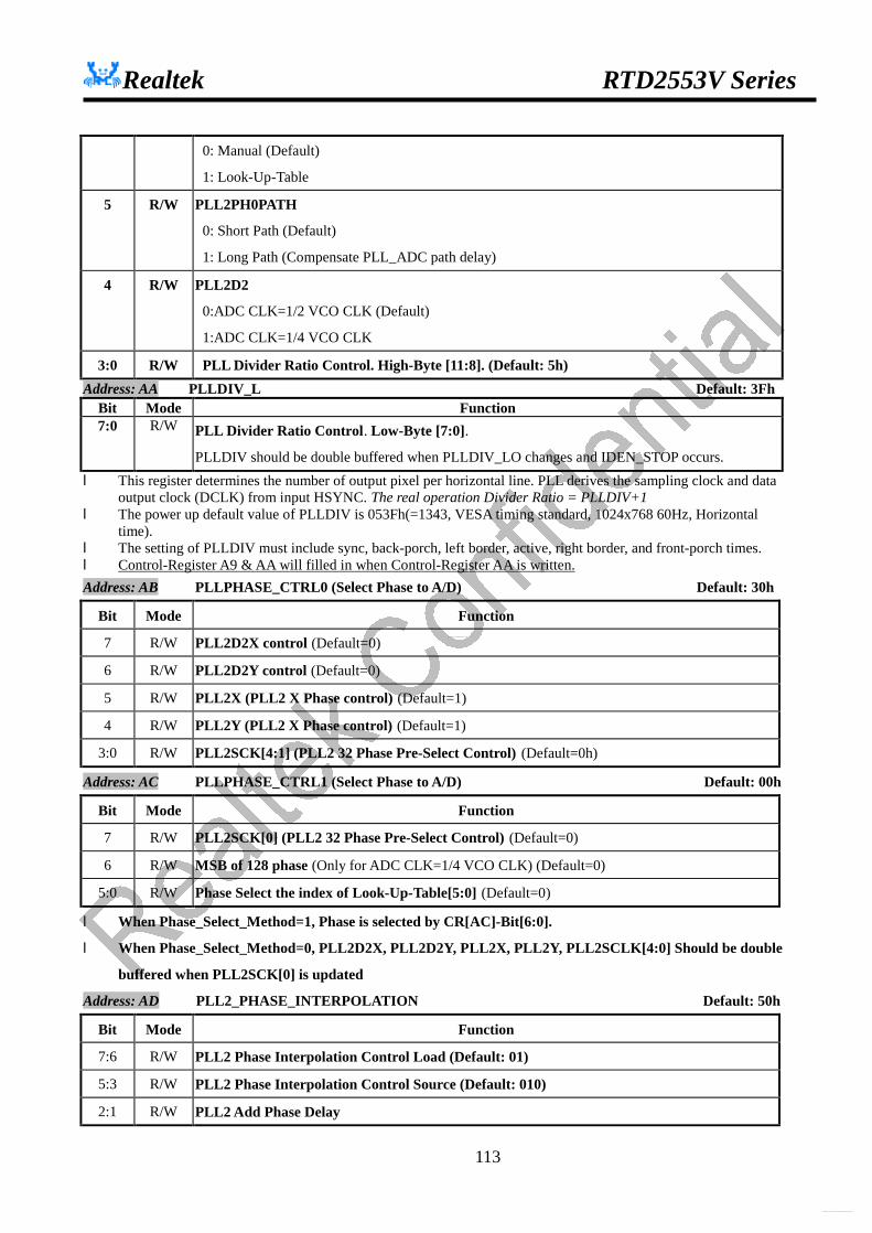
Realtek RTD2553V Series
113
0: Manual (Default)
1: Look-Up-Table
5 R/W PLL2PH0PATH
0: Short Path (Default)
1: Long Path (Compensate PLL_ADC path delay)
4 R/W PLL2D2
0:ADC CLK=1/2 VCO CLK (Default)
1:ADC CLK=1/4 VCO CLK
3:0 R/W PLL Divider Ratio Control. High-Byte [11:8]. (Default: 5h) Address: AA PLLDIV_L Default: 3Fh
Bit Mode Function 7:0 R/W PLL Divider Ratio Control. Low-Byte [7:0].
PLLDIV should be double buffered when PLLDIV_LO changes and IDEN_STOP occurs. l This register determines the number of output pixel per horizontal line. PLL derives the sampling clock and data
output clock (DCLK) from input HSYNC. The real operation Divider Ratio = PLLDIV+1 l The power up default value of PLLDIV is 053Fh(=1343, VESA timing standard, 1024x768 60Hz, Horizontal
time). l The setting of PLLDIV must include sync, back-porch, left border, active, right border, and front-porch times. l Control-Register A9 & AA will filled in when Control-Register AA is written. Address: AB PLLPHASE_CTRL0 (Select Phase to A/D) Default: 30h
Bit Mode Function
7 R/W PLL2D2X control (Default=0)
6 R/W PLL2D2Y control (Default=0)
5 R/W PLL2X (PLL2 X Phase control) (Default=1)
4 R/W PLL2Y (PLL2 X Phase control) (Default=1)
3:0 R/W PLL2SCK[4:1] (PLL2 32 Phase Pre-Select Control) (Default=0h)
Address: AC PLLPHASE_CTRL1 (Select Phase to A/D) Default: 00h
Bit Mode Function
7 R/W PLL2SCK[0] (PLL2 32 Phase Pre-Select Control) (Default=0)
6 R/W MSB of 128 phase (Only for ADC CLK=1/4 VCO CLK) (Default=0)
5:0 R/W Phase Select the index of Look-Up-Table[5:0] (Default=0)
l When Phase_Select_Method=1, Phase is selected by CR[AC]-Bit[6:0].
l When Phase_Select_Method=0, PLL2D2X, PLL2D2Y, PLL2X, PLL2Y, PLL2SCLK[4:0] Should be double
buffered when PLL2SCK[0] is updated
Address: AD PLL2_PHASE_INTERPOLATION Default: 50h
Bit Mode Function
7:6 R/W PLL2 Phase Interpolation Control Load (Default: 01)
5:3 R/W PLL2 Phase Interpolation Control Source (Default: 010)
2:1 R/W PLL2 Add Phase Delay
http://www.DataSheet4U.net/
datasheet pdf - http://www.DataSheet4U.net/
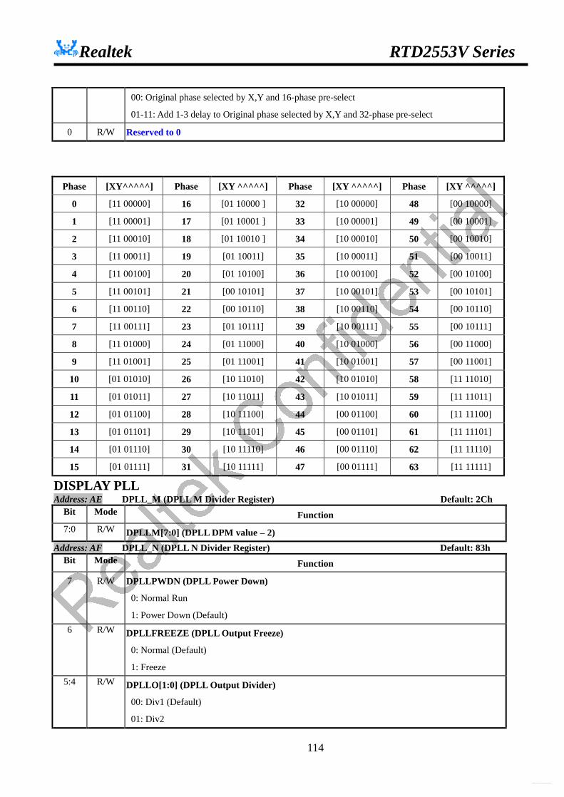
Realtek RTD2553V Series
114
00: Original phase selected by X,Y and 16-phase pre-select
01-11: Add 1-3 delay to Original phase selected by X,Y and 32-phase pre-select
0 R/W Reserved to 0
Phase [XY^^^^^] Phase [XY ^^^^^] Phase [XY ^^^^^] Phase [XY ^^^^^]
0 [11 00000] 16 [01 10000 ] 32 [10 00000] 48 [00 10000]
1 [11 00001] 17 [01 10001 ] 33 [10 00001] 49 [00 10001]
2 [11 00010] 18 [01 10010 ] 34 [10 00010] 50 [00 10010]
3 [11 00011] 19 [01 10011] 35 [10 00011] 51 [00 10011]
4 [11 00100] 20 [01 10100] 36 [10 00100] 52 [00 10100]
5 [11 00101] 21 [00 10101] 37 [10 00101] 53 [00 10101]
6 [11 00110] 22 [00 10110] 38 [10 00110] 54 [00 10110]
7 [11 00111] 23 [01 10111] 39 [10 00111] 55 [00 10111]
8 [11 01000] 24 [01 11000] 40 [10 01000] 56 [00 11000]
9 [11 01001] 25 [01 11001] 41 [10 01001] 57 [00 11001]
10 [01 01010] 26 [10 11010] 42 [10 01010] 58 [11 11010]
11 [01 01011] 27 [10 11011] 43 [10 01011] 59 [11 11011]
12 [01 01100] 28 [10 11100] 44 [00 01100] 60 [11 11100]
13 [01 01101] 29 [10 11101] 45 [00 01101] 61 [11 11101]
14 [01 01110] 30 [10 11110] 46 [00 01110] 62 [11 11110]
15 [01 01111] 31 [10 11111] 47 [00 01111] 63 [11 11111]
DISPLAY PLL Address: AE DPLL_M (DPLL M Divider Register) Default: 2Ch
Bit Mode Function 7:0 R/W DPLLM[7:0] (DPLL DPM value – 2)
Address: AF DPLL_N (DPLL N Divider Register) Default: 83h Bit Mode Function
7 R/W DPLLPWDN (DPLL Power Down)
0: Normal Run
1: Power Down (Default) 6 R/W DPLLFREEZE (DPLL Output Freeze)
0: Normal (Default)
1: Freeze 5:4 R/W DPLLO[1:0] (DPLL Output Divider)
00: Div1 (Default)
01: Div2
http://www.DataSheet4U.net/
datasheet pdf - http://www.DataSheet4U.net/
Realtek RTD2553V Series
115
10: Div4
11: Div8 3:0 R/W DPLLN[7:0] (DPLL DPN value – 2) (Default: 3h)
l Assume DPLL_M=0x7D, DPM=0x7D+2=127; DPLL_N=0x0A, DPN=0x0A+2=12; Divider=1/4, F_IN = 24.576MHz. F_DPLL = F_IN x DPM / DPN x Divider = 24.576 x 127 / 12 / 4 = 65.024MHz.
l If LPF_Mode = 1, suppose DPM=110, DPN = 12, Ich = Idch[000100] = 6.25uA, DPLL=225MHz, then DPM / Ich =17.6. Please keep the ratio as constant.
l If LPF_Mode = 0, suppose DPM=46, DPN = 5, Ich = Idch [101010] =27.5uA, DPLL=226MHz, then DPM / Ich = 1.67. Please keep the ratio as constant.
Address: B0 DPLL_CRNT (DPLL Current/Resistor Register) Default: C8h Bit Mode Function 7:6 R/W DPLLVR[1:0] (DPLL Loop Filter Resister Control)
00: 16K (LPF Mode = 0), 46K (LPF Mode = 1)
01: 18K (LPF Mode = 0), 53K (LPF Mode = 1)
10: 20K (LPF Mode = 0), 60K (LPF Mode = 1)
11: 22K (LPF Mode = 0), 67K (LPF Mode = 1) (Default) 5:4 Reserved 3:0 R/W DPLLSI[3:0] (DPLL Charger Pump Current IchDpll) (Default: 1000)
Icp=(1uA+1uA*bit[0]+2uA*bit[1]+4uA*bit[2]+8uA*bit[3]) l Keep Icp/DPM constant Address: B1 DPLL_WD (Watch Dog Register) Default: 16h
Bit Mode Function 7 R DPLLSTATUS (DPLL WD Status)
0: Normal
1: Abnormal 6 R/W DPLLWDRST (DPLL WD Reset)
0: Normal (Default)
1: Reset 5 R/W DPLLWDSET (DPLL WD Set)
0: Normal (Default)
1: Set 4:3 R/W DPLLWDVSET[1:0] (DPLL WD Voltage Set)
00: 0.58V
01: 0.74V
10: 0.88V (Default)
11: 1.17V 2 R/W DPLLUPDN (DPLL Frequency Tuning Up/Down)
0: Freq Up
1: Freq Down (Default)
http://www.DataSheet4U.net/
datasheet pdf - http://www.DataSheet4U.net/

Realtek RTD2553V Series
116
1 R/W DPLLSTOP (DPLL Frequency Tuning Enable)
0: Disable
1: Enable (Default)
Turn on before CRBB[0]. 0 R/W DPLLLPFMODE (DPLL LPF Mode)
0: DPN<=5 è LPFMode=0 Ich=9.15uA DPM=46 DPN=5 (Default)
1: 16>=DPN>=5 è LPFMode=1 Ich=3.2uA DPM=110 DPN=12 Address: B2 DPLL Other default: 04h
Bit Mode Function
7:5 -- Reserved
4 R/W DPLL Clock to SSCG
0: DPLLVCO/4 (Defalult)
1: ( DPLLVCO+Phase_Swallow )/4
3 R/W DPLL Reference Frequency Select
0: Original Crystal Clock (Default)
1: Clock After M2PLL
2 R/W DPLL VCO RON (increase VCO_OP Phase Margin)
0: Disable
1: Enable (Default)
1 R/W DPLL VCO START (startup VCO)
0: Disable (Default)
1: Enable
0 R/W DPLL BPN (DPLL dividend enable)
0: DPLL_N dividend enable
1: N dividend disable
MULTIPLY PLL FOR INPUT CYRSTAL Address: B3 M2PLL_ADDR_PORT
Bit Mode Function
7:3 -- Reserved
2:0 R/W Address for M2PLL access
Address: B4 M2PLL_DATA _PORT
Bit Mode Function
7:0 R/W Data Port for M2PLL Address: B4-00 MULTI_PLL_CTRL0 Default: 92h
http://www.DataSheet4U.net/
datasheet pdf - http://www.DataSheet4U.net/

Realtek RTD2553V Series
117
Bit Mode Function
7:3 R/W M2PLL M Code[4:0]-2 (DPM) (shall not be 0)
Default = 20 => 10010
2 R/W M2PLL Power Down
0: Normal Run (Default)
1: Power Down
1 R/W M2PLL N Code
0: N=1
1: N=2 (Default)
0 R/W Reserved to 0 VCO range = 120MHz ~ 250MHz FIF0_ clock = Fxtal_ * M2PLL_M / M2PLL_N POR clock = Fxtal * M2PLL_M / M2PLL_N / 8 Address: B4-01 MULTI_PLL_CTRL1 Default: 94h
Bit Mode Function
7:6 R/W M2PLL Loop Filter Resistor Control
00: 15K
01: 18K
10: 21K(Default)
11: 24K
5:4 R/W M2PLL Loop Filter Charge Current Control(Default:01)
Icp=5uA+5uA*bit[4]+10uA*bit[5]
i.e.: Keep Icp/DPM constant
3:2 R/W M2PLL WD Voltage
00: 0.80V
01: 1.0V (Default)
10: 1.2V
11: 1.4V
1 R/W M2PLL_WDRST
0: Normal (Default)
1: Reset ( M2PLL Function as a Normal PLL, regardless WD)
0 R/W M2PLL_WDSET
0: Normal (Default)
1: Set (Free Run by WD asserts VCO Voltage) Address: B4-02 MULTI_PLL_CTRL1 Default: 40h
Bit Mode Function
http://www.DataSheet4U.net/
datasheet pdf - http://www.DataSheet4U.net/
Realtek RTD2553V Series
118
7 R M2PLL WD Status
0: Normal
1: Abnormal
6 R/W M2PLL Output Freeze (FIFO clock)
0: Normal (Default)
1: Freeze
i.e.: when output is frozen, the internal PLL is still operating
5:0 -- reserved
CRB4-00~02 are not controlled by software reset.
PLL TEST Address: B4-03 PLL_TEST (PIN3) Default: 19h
Bit Mode Function 7:6 -- Reserved to 0 5 R/W PLL_TP1_FAST (PLL_TestPin1 TTL Output Driving)
0: Slow (Default)
1: Fast 4:3 R/W PLL_TP1_MODE[1:0] (PLL_TestPin1 I/O Mode Select)
00: Analog In/Out
01: Open drain Output
10: Digital TTL Output
11: Digital TTL Input (3V) →Power on latch to determine MCU direction (Default)
2:0 R/W PLL_TP1_MUX[2:0] (PLL_TestPin1 Output Signal Select)
000: DPLL Clock
001: PLL1 Status
010: FAV clock(From PLL1)
011: PLL2 Status
100: HSOUT
101: ADC clock (from PLL2)
110: EMPTY FLAG(DDC/CI BUFFER)
111: Normal Operation Usage (Refer to pin share control)
Address: B4-04 PLL_TEST (PIN4) Default: 19h Bit Mode Function 7 -- Reserved to 0
6 R/W Select the external clock source instead of DPLL clock for MP test (Digital TTL input)
0: Disable
1: Enable
http://www.DataSheet4U.net/
datasheet pdf - http://www.DataSheet4U.net/
Realtek RTD2553V Series
119
5 R/W PLL_TP2_FAST (PLL_TestPin1 TTL Output Driving)
0: Slow
1: Fast 4:3 R/W PLL_TP2_MODE[1:0] (PLL_TestPin2 I/O Mode Select)
00: Analog In/Out
01: Open drain Output
10: Digital TTL Output
11: Digital TTL Input (3V) (Default) 2:0 R/W PLL_TP2_MUX[2:0] (PLL_TestPin2 Output Signal Select)
000: PLL1 Clock
001: DPLL Status
010: PLL2 Phase0 clock
011: M2PLL clock
100: HSFB
101: Normal Operation Usage (Refer to pin share control)
110: FULL FLAG(DDC/CI BUFFER)
111: DCLK/4
DCLK Spread Spectrum Address: B5 DCLK_FINE_TUNE_OFFSET_MSB Default: 00h
Bit Mode Function 7:6 -- Reserved 5 R/W Only Even / Odd Field Mode Enable
0: Disable (Default)
1: Enable 4 R/W Even / Odd Field Select
0: Even (Default)
1: Odd 3:0 R/W DCLK Offset [11:8] in Fixed Last Line DVTOTAL & DHTOTAL
Address: B6 DCLK_FINE_TUNE_OFFSET_LSB Default: 00h Bit Mode Function 7:0 R/W DCLK Offset [7:0] in Fixed Last Line DVTOTAL & DHTOTAL
Address: B7 SPREAD_SPECTRUM Default: 00h Bit Mode Function 7:4 R/W DCLK Spreading range (0.0~7.5%)
The bigger setting, the spreading range will bigger, but not uniform
http://www.DataSheet4U.net/
datasheet pdf - http://www.DataSheet4U.net/
Realtek RTD2553V Series
120
3 R/W Spread Spectrum FMDIV (SSP_FMDIV)//(0)
0: 33K
1: 66K 2 R/W Spread Spectrum Setting Ready for Writing (Auto Clear)
0: Not ready
1: Ready to write 1:0 R/W Frequency Synthesis Select (F & F-N*dF)
00~11: N=1~4 l The “Spread Spectrum Setting Ready for Writing” means 4 kinds of registers will be set after this bit is set:
1. DCLK spreading range 2. Spread spectrum FMDIV 3. DCLK offset setting 4. Frequency synthesis select
Address: B8 FIXED_LAST_LINE_MSB Bit Mode Function 6:4 R/W Fixed Last Line Length [11:8] 3:0 R/W Fixed DVTOTAL [11:8]
Address: B9 FIXED_LAST_LINE_DVTOTAL _LSB Bit Mode Function 7:0 R/W Fixed DVTOTAL [7:0]
Address: BA FIXED_LAST_LINE_ LENGTH_LSB Bit Mode Function 7:0 R/W Fixed Last Line Length [7:0]
l Fixed last line value can’t be zero, and can’t smaller than DH_Sync width.
Address: BB FIXED_LAST_LINE_CTRL Default: 00h 7:4 -- Reserved to 0 3 R/W Enable New Design Function in Fixed Last Line Mode
0: Disable (Default)
1: Enable 2 R/W DDS Spread Spectrum Test Enable
0: Disable (Default)
1: Enable 1 R/W Enable the Fixed DVTOTAL & Last Line DHTOTAL Function
0: Disable (Default)
1: Enable 0 R/W Enable DDS Spread Spectrum Output Function
0: Disable (Default)
1: Enable
http://www.DataSheet4U.net/
datasheet pdf - http://www.DataSheet4U.net/
Realtek RTD2553V Series
121
Procedure:
l First, we have set M/N code and then we need to tune DCLK OFFSET to achieve frame-sync, every step of offset
frequency is DCLK/ 152 . l When we finished the frame-sync, we turn on CR BB[1] to let the system running in to free-run mode, at this time,
the CRB8,CRB9,CRBA are the reference DV and DH total and Fixed last Line Length.
l But the free-run mode DVS’ should be close to frame-sync mode DVS to achieve pseudo-frame-sync( actually, it
is free run mode now)
l Then we use CRB7 [1:0] (F-N*dF) to keep DVS’ and DVS very closely to achieve pseudo-frame-sync.
Notice:
l In RTD2523, when all the setting above is ready, then we open spread spectrum function, the DCLK OFFSET will
shift, please keep the DCLK OFFSET keeps steady when we open spread spectrum function.
l In Real free-run mode, the DV_TOTAL refers to CR32/CR33, and in Fixed-Last-Line mode, the free-run timing
DV_TOTAL refers to CRB8/CRB9, at this time CR35/36 serve for Vsync-timeout watch dog reference.
http://www.DataSheet4U.net/
datasheet pdf - http://www.DataSheet4U.net/
Realtek RTD2553V Series
122
Embedded TMDS
Address: BC TMDS_MEASURE_SELECT Default: 00h Bit Mode Function
7 R/W Transition measurement method
0: measure the number of transition for N-clock duration (CRBC[3:0])
1: measure the number of transition smaller than 16/64 clock period (CRBD[0]) for 1-frame
duration
6:4 R/W Measure times(exponential of 2)
000: 1
001: 2
010: 4
011: 8
100: 16
101: Not available
110: Not available
111: Not available
3:0 R/W Numbers of Clock Period, measurement duration (where clock frequency is 12Khz)
0000: 16
0001: 1
0010: 2
0011: 3
…….
1111: 15
This function will do bit [6:4] times, each time lasts for bit [3:0]/12 ms.
Address: BD TMDS_MEAS_RESULT0 Default: 0000_0110b
Bit Mode Function
7 R/W Transition measurement
0:Stop measure, Cleared after finish (Default)
1:Start measure
6:5 R/W Measure Result Select
00: AVE Value (Default)
01: Max Value
10: Min Value
4:3 R/W Measure Select
00: Measure Hsync transition times before error correction.
http://www.DataSheet4U.net/
datasheet pdf - http://www.DataSheet4U.net/
Realtek RTD2553V Series
123
01: Measure Hsync transition times after error correction.
10: Measure Data Enable transition times before error correction.
11: Measure Data Enable transition times after error correction.
2 R/W Clock DC Offset
0: Disable
1: Enable DC Offset Compensation
1 R/W R/G/B DC Offset
0: Disable
1: Enable DC Offset Compensation
0 R/W Criterion of Transition Count, duration smaller than
0: 16 clock
1: 64 clock
Address: BE TMDS_MEAS_RESULT1
Bit Mode Function
7 --- Reserved
6:0 R Value of measure result[6:0] (Item refer to CRBD[6:5])
Address: BF TMDS_CTRL Bit Mode Function 7 R B channel detect (DE low 128 clock)(write clear)
0: no
1: yes 6 R G channel detect (DE low 128 clock)(write clear)
0: no
1: yes 5 R R channel detect (DE low 128 clock)(write clear)
0: no
1: yes 4 R Hsync occur(write clear)
0: no
1: yes 3 R Vsync occur(write clear)
0: no
1: yes
2:0 Reserved
http://www.DataSheet4U.net/
datasheet pdf - http://www.DataSheet4U.net/

Realtek RTD2553V Series
124
ERRORCORRECTION
HS_DEC
VS_DEC
HS'
VS'
MUXHS_Gen
VS_Gen
H/V occur flag
DE_Only
Address: C0 CRC_OUTPUT_BYTE_2 Bit Mode Function 7:0 R/W 1st read=> Output CRC-24 bit 23~16
2nd read=> Output CRC-24 bit 15~8
3rd read=> Out put CRC-24 bit 7~0 l The read pointer should be reset when 1. CRC Output Byte is written 2. CRC Check starts.
l The read back CRC value address should be auto-increase, the sequence is shown above
Address: C1 TMDS_OUTPUT_CTRL Default: 00h Bit Mode Function 7 R/W Auto Output Enable
0: Disable (Default)
1: Enable 6 R/W TMDS R Channel Output Enable
0: Disable (Default)
1: Enable 5: R/W TMDS G Channel Output Enable
0: Disable (Default)
1: Enable 4 R/W TMDS B Channel Output Enable
0: Disable (Default)
1: Enable 3 R/W OCLK Enable
0: Disable (Default)
1: Enable
http://www.DataSheet4U.net/
datasheet pdf - http://www.DataSheet4U.net/
Realtek RTD2553V Series
125
2 R/W OCLK Invert enable
0: Normal (Default)
1: Enable 1 R/W Reserved 0 R/W CLK25XINV
0: No Invert (Default)
1: Invert
Address: C2 POWER_ON_OFF_CTRL Default: 20h Bit Mode Function 7 R/W DE-only: Generate VS/HS from DE signal
0: Disable (Default)
1: Enable 6 R/W B/R channel swap
0: No swap (Default)
1: Swap 5 R/W Input Channel control by auto function
0: Manual
1: Auto (Default) 4 R/W Enable Clock channel: turn on clock channel PLL (For manual use)
0: Disable (Default)
1: Enable 3 R/W Enable Red input port (For manual use, cut off 50ohm internal resistor)
0: Disable (Default)
1: Enable 2 R/W Enable Green input port (For manual use, cut off 50ohm internal resistor)
0: Disable (Default)
1: Enable 1 R/W Enable Blue input port (For manual use, cut off 50ohm internal resistor)
0: Disable (Default)
1: Enable 0 R/W CRC check
0: Stop
1: Start CRC check during the next full frame and clear after finish (CRC value in reg. 0xC0)
Address: C3 ANALOG_COMMON_CTRL0 Default: 03h Bit Mode Function
http://www.DataSheet4U.net/
datasheet pdf - http://www.DataSheet4U.net/

Realtek RTD2553V Series
126
7:4 R RESL<3:0> Z0 value
0000: max.
1111: min.
Read back Z0 value when calibration is finished. 3:0 R/W SPADL<3:0>: Selection TSTPAD mode for analog test
0000: 40u
0001: select TMDS test signal (Please reference CRC4 5)
0010: D2PL(For PWM0/TCON2) (pin 5)
x011: P2DL (Pad to Digital, Digital input 3.3V) (Default) power on latch
x1xx: HZ
1000: A2P33V
1001: D2P33V in open drain mode
1010: D2P33V in TTL mode
Address: C4 ANALOG_COMMON_CTRL1 Default: 00h Bit Mode Function 7:6 R/W TMDS_TEST Normal Output Selection
00: PWM0
01: TCON2
10: IRQ#
11: Rsv 5 R/W ENTSTL: enable internal test signal list below
0: off
1: on 4:0 R/W SPADTSTL<4:0>: select test signal (SPADL<3:0>=0001b)
00x00 CLKPLLPOWL 10010 Fin in green port
00x01 LPRST in clk port 10011 Fbak in green port
00x10 Fin in clk port 10100 Ck2.5x sampling clk in green port
00x11 Fbak in clk port 10101 Ck2.5x in green port
01000 BLUPOWL 10110 Ck1.0x in green port
01001 LPRST in blue port 10111 Ck0.5x in green port
01010 Fin in blue port 11000 REDPOWL
01011 Fbak in blue port 11001 LPRST in red port
01100 Ck2.5x sampling clk in blue 11010 Fin in red port
01101 Ck2.5x in blue port 11011 Fbak in red port
01110 Ck1.0x in blue port 11100 Ck2.5x sampling clk in red port
01111 Ck0.5x in blue port 11101 Ck2.5x in red port
10000 GRNPOWL 11110 Ck1.0x in red port
http://www.DataSheet4U.net/
datasheet pdf - http://www.DataSheet4U.net/
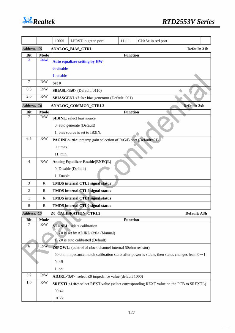
Realtek RTD2553V Series
127
10001 LPRST in green port 11111 Ck0.5x in red port Address: C5 ANALOG_BIAS_CTRL Default: 31h
Bit Mode Function 7 R/W Auto equalizer setting by HW
0: disable
1: enable 7 R/W Set 0
6:3 R/W SBIASL<3:0> (Default: 0110) 2:0 R/W SBIASGENL<2:0>: bias generator (Default: 001)
Address: C6 ANALOG_COMMON_CTRL2 Default: 2xh Bit Mode Function 7 R/W SIBINL: select bias source
0: auto generate (Default)
1: bias source is set to IB2IN. 6:5 R/W PAGINL<1:0>: preamp gain selection of R/G/B port (Default=01)
00: max.
11: min.
4 R/W Analog Equalizer Enable(ENEQL)
0: Disable (Default)
1: Enable
3 R TMDS internal CTL3 signal status
2 R TMDS internal CTL2 signal status
1 R TMDS internal CTL1 signal status
0 R TMDS internal CTL0 signal status
Address: C7 Z0_CALIBRATION_CTRL2 Default: A3h Bit Mode Function 7 R/W STUNEL: select calibration
0: Z0 is set by ADJRL<3:0> (Manual)
1: Z0 is auto calibrated (Default) 6 R/W Z0POWL: (control of clock channel internal 50ohm resistor)
50 ohm impedance match calibration starts after power is stable, then status changes from 0→1
0: off
1: on 5:2 R/W ADJRL<3:0>: select Z0 impedance value (default 1000) 1:0 R/W SREXTL<1:0>: select REXT value (select corresponding REXT value on the PCB to SREXTL)
00:4k
01:2k
http://www.DataSheet4U.net/
datasheet pdf - http://www.DataSheet4U.net/

Realtek RTD2553V Series
128
10:4k/3
11:1k Address: C8 CLOCK_PLL_SETTING Default: 32h
Bit Mode Function 7 --- Reserved to 0
6:5 R/W SCKLVCSETL<1:0>: when reset CLK PLL, the reset value of VC node
00: 2.17V
01: 1.98V (Default)
10: 1.79V
11: 1.60V 4:2 R/W SCKIL<2:0>: PLL charge-pump current (Default= 3’b100)
10u + <4>*20u + <3>*10u + <2>*10u 1:0 R/W SCKRL<1:0>: PLL LPF resistor
8k + <1>*4k + <0>*2k
Address: C9 RGB_PLL_SETTING Default: 28h Bit Mode Function 7 --- Reserved to 0
6:5 R/W SSAVCSETL<1:0>: when reset R/G/B PLL, the reset value of VC node
00: 2.17
01: 1.98 (Default)
10: 1.79
11: 1.60 4:2 R/W SSAIL<2:0>: PLL charge-pump current (Default:3’b010)
10u+<4>*20u+<3>*10u+<2>*10u 1:0 R/W SSARL<1:0>: PLL LPF resistor (Default: 2’b00)
8k+<1>*4k+<0>*2k
Address: CA WATCH_DOG_CTRL Default: 40h Bit Mode Function 7 --- Reserved to 0
6 R/W FIFO R/W Auto Calibration
0: Manual
1: Auto (Default)
5 R/W R Channel Manual Mode
0: Not Invert (Default)
1: Invert
4 R/W G Channel Manual Mode
0: Not Invert (Default)
http://www.DataSheet4U.net/
datasheet pdf - http://www.DataSheet4U.net/
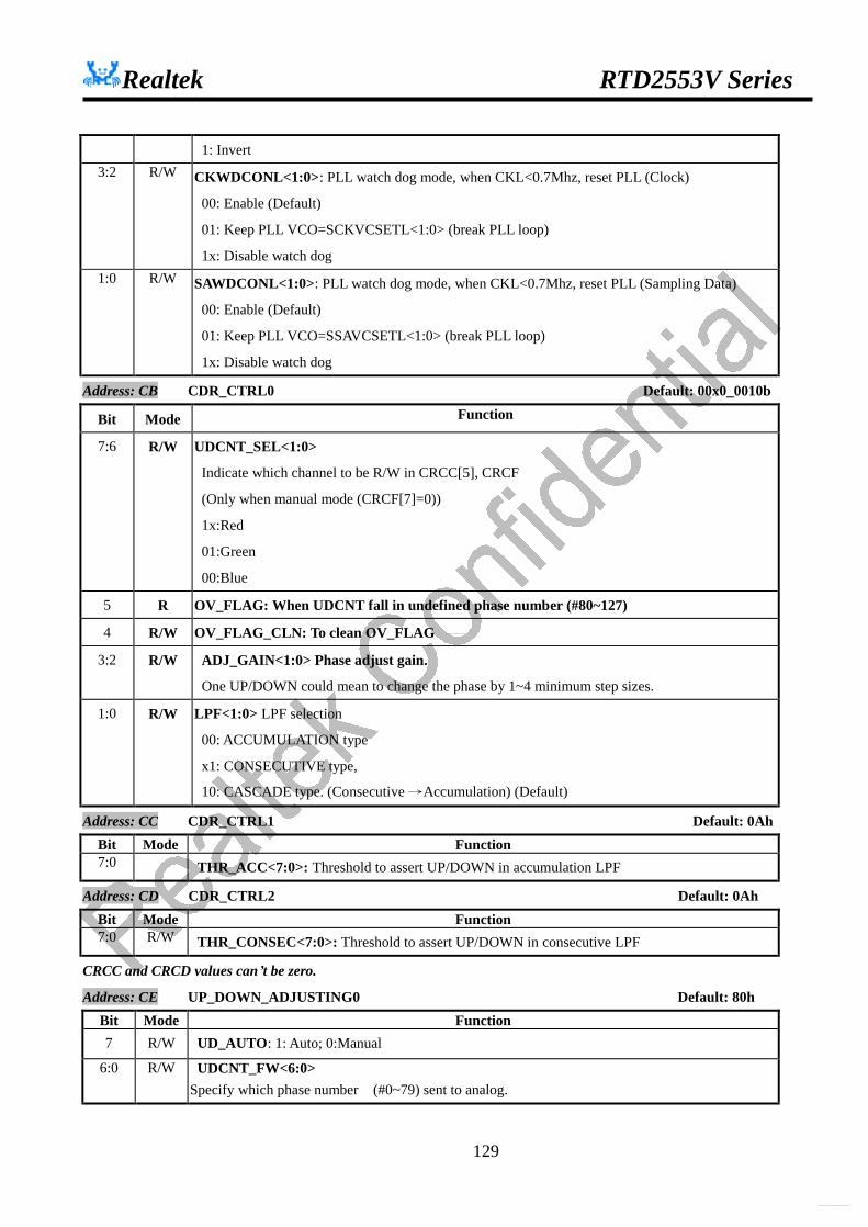
Realtek RTD2553V Series
129
1: Invert 3:2 R/W CKWDCONL<1:0>: PLL watch dog mode, when CKL<0.7Mhz, reset PLL (Clock)
00: Enable (Default)
01: Keep PLL VCO=SCKVCSETL<1:0> (break PLL loop)
1x: Disable watch dog 1:0 R/W SAWDCONL<1:0>: PLL watch dog mode, when CKL<0.7Mhz, reset PLL (Sampling Data)
00: Enable (Default)
01: Keep PLL VCO=SSAVCSETL<1:0> (break PLL loop)
1x: Disable watch dog
Address: CB CDR_CTRL0 Default: 00x0_0010b
Bit Mode Function
7:6 R/W UDCNT_SEL<1:0>
Indicate which channel to be R/W in CRCC[5], CRCF
(Only when manual mode (CRCF[7]=0))
1x:Red
01:Green
00:Blue
5 R OV_FLAG: When UDCNT fall in undefined phase number (#80~127)
4 R/W OV_FLAG_CLN: To clean OV_FLAG
3:2 R/W ADJ_GAIN<1:0> Phase adjust gain.
One UP/DOWN could mean to change the phase by 1~4 minimum step sizes.
1:0 R/W LPF<1:0> LPF selection
00: ACCUMULATION type
x1: CONSECUTIVE type,
10: CASCADE type. (Consecutive →Accumulation) (Default)
Address: CC CDR_CTRL1 Default: 0Ah Bit Mode Function 7:0 THR_ACC<7:0>: Threshold to assert UP/DOWN in accumulation LPF
Address: CD CDR_CTRL2 Default: 0Ah Bit Mode Function 7:0 R/W THR_CONSEC<7:0>: Threshold to assert UP/DOWN in consecutive LPF
CRCC and CRCD values can’t be zero.
Address: CE UP_DOWN_ADJUSTING0 Default: 80h Bit Mode Function 7 R/W UD_AUTO: 1: Auto; 0:Manual
6:0 R/W UDCNT_FW<6:0> Specify which phase number (#0~79) sent to analog.
http://www.DataSheet4U.net/
datasheet pdf - http://www.DataSheet4U.net/

Realtek RTD2553V Series
130
Address: CF UP_DOWN_ADJUSTING1 Default: 14h Bit Mode Function 7:0 R/W WAIT_TIME<7:0>: The minimum period between two phases adjusts.
(phase change responding time)
Address: D0 Adaptive Equalizer Default: 00h Bit Mode Function 7 R/W Adaptive Equalizer Enable
0: disable
1: enable 6:5 R Adaptive Equalizer up/down by HW (cleared by writing CRC6)
00: the same
01: down
1x: up 4:2 R/W Accumulative Times
000: 8
001: 16
…
111: 64
1:0 R/W HDCP MP Test
Address: D1 UP_DOWN_CTRL0 Default: 92h Bit Mode Function 7 R/W ADJ_AUTO_R: Phase adjusting automatically by digital or not, for RED channel.
1: automatic (Default)
0: manual by firmware 6:5 R/W UPDOWN_R<1:0>: Manually adjust of up/down for PLL, in RED channel. This is only useful when
ADJ_AUTO_R is set to 0.
10: UP
01: DOWN
00: hold (Default) 4 R/W ADJ_AUTO_G : Phase adjusting automatically by digital or not, for GREEN channel.
1: automatic (Default)
0: manual by firmware 3:2 R/W UPDOWN_G<1:0>: Manually adjust of up/down for PLL, in GREEN channel. This is only useful
when ADJ_AUTO_R is set to 0.
10: UP
01: DOWN
http://www.DataSheet4U.net/
datasheet pdf - http://www.DataSheet4U.net/

Realtek RTD2553V Series
131
00: hold (Default)
1 R/W ADJ_AUTO_B :Phase adjusting automatically by digital or not, for BLUE channel.
1: automatic (Default)
0: manual by firmware 0 R/W UP side DOWN
0: Disable
1: Enable Address: D2 UP_DOWN_CTRL1 Default: 0001_xxxxb Bit Mode Function
7:6 R/W UPDOWN_B<1:0>:
Manually adjust of up/down for PLL, in BLUE channel. This is only useful when ADJ_AUTO_R is
set to 0.
10: UP
01: DOWN
00: hold 5 R/W Reserved to 0 4 R/W NL_AUTO : Frequency range selection by digital part automatically.
1: automatic by digital (Default)
0: manual selected by firmware 3:0 R NL<3:0>: Frequency selected by digital part.
0000: 0Hz
0001: >165MHz or <25MHz
1110: 25-50 MHz
1000: 50-80 MHz
0110: 80-112 MHz
0100: 112-140 MHz
0011: 140-165 MHz
otherwise: invalid
Address: D3 UP_DOWN_CTRL2 Default: 30h Bit Mode Function
7 R/W CPTEST
0: normal mode, in which clock and data from analog are used.
1: select TSTCKIN/TSTDIN as input 2X5 clock and data respectively, for TESTING. 6:4 R/W STABLE_CNT<2:0>: Numbers of consecutive frequency change command after which N_FREQ
can be adjusted.
http://www.DataSheet4U.net/
datasheet pdf - http://www.DataSheet4U.net/

Realtek RTD2553V Series
132
3:0 R/W NL_FW<3:0>: Frequency selected by firmware. The valid values are the same as those listed in
previous row. (Read back value in CRD3)
Address: D4 UP_DOWN_CRTL3 Default: 00h Bit Mode Function 7:6 R/W ERRC_SEL<1:0>
00: original signal
01: debouncing 1 cycle
10: debouncing 1+8 cycle
11: 1+8 cycle debouncing+ DE masking transition of vs/hs+vs+(hs88) to masking DE 5:0 R/W DEBUG_SEL
HDCP Address: D5 HDCP CTRL default : 0000_0000b
Bit Mode Function
7 R/W HDCP Key Access SRAM BIST Action
0: stop & clear after finish.
1: start
6 R HDCP Key Access SRAM BIST Status
0: Fail
1: OK, when test start, clear this bit
5 R Indicate VSYNC Polarity
0: Positive, which means VS pulse is high.
1: Negative
4 R/W Invert VSYNC for HDCP
0: Not Inverted
1: Inverted
3 R/W Indicate VSYNC Polarity Mode:
0: auto, indicate by 0x70[5]
1: manual, decided by 0x70[4]
2 R/W MCU Access DDC data first
0: enable DDC channel and MCU access only when DDC is not busy
1: disable DDC channel and MCU access only
1 R/W Device Key Access Port download enable
0: disable, this would reset the address of Device Key Access Port to 0.
1: enable
0 R/W HDCP Enable
0: Disable HDCP, except for output.
1: Auto Enable HDCP function, when Tx I2C write Aksv
http://www.DataSheet4U.net/
datasheet pdf - http://www.DataSheet4U.net/

Realtek RTD2553V Series
133
Address: D6 Device Key Access Port
Bit Mode Function
7:0 R/W When enable device key accessing 40x56 table, the 56-bit key table will be transferred to 64-bit
pseudo data with 7th, 15th, 23rd, 31st, 39th, 47th, 55th bits inserted.
The inserted data are ‘0’.And the write sequence is:
{D0-Byte0, D0-Byte1, D0-Byte2, D0-Byte3,D0-Byte4, D0-Byte5, D0-Byte6, D0-Byte7},
{D1-Byte0, D1-Byte1, 1-Byte2,D1-Byte3,
D1-Byte4, D1-Byte5, D1-Byte6, D1-Byte7},
……………………………………………
Accessing this port must be coded/decoded by REALTEK protection code.
Address: D7 HDCP_PORT_CTRL default: 00h
Bit Mode Function
7:1 -- Reserved
0 R/W HDCP accessing port auto increase (For Host Side)
0: auto increase
1: keep in the same address.
Address: D8 HDCP_ADDR_PORT default: 00h
Bit Mode Function
7:0 R/W Address port for embedded HDCP access, auto increase after DATA_PORT being accessed . (For
Host Side controlled by D7)
Address: D9 HDCP_DATA_PORT
Bit Mode Function
7:0 R/W Data port for embedded HDCP access
I2C Control Register Map ( MCU Side )
Hex
Address
Write/
Read
Size
in
Bytes
Default
value
Register
Name
Function
0x00 R/W 5 XX_XX_XX BKSV HDCP Receiver KSV. This value may be used to determine that the
http://www.DataSheet4U.net/
datasheet pdf - http://www.DataSheet4U.net/
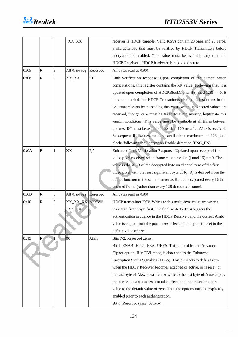
Realtek RTD2553V Series
134
_XX_XX receiver is HDCP capable. Valid KSVs contain 20 ones and 20 zeros,
a characteristic that must be verified by HDCP Transmitters before
encryption is enabled. This value must be available any time the
HDCP Receiver’s HDCP hardware is ready to operate.
0x05 R 3 All 0, no reg Reserved All bytes read as 0x00
0x08 R 2 XX_XX Ri’ Link verification response. Upon completion of the authentication
computations, this register contains the R0' value. Following that, it is
updated upon completion of HDCPBlockCipher if (i mod 128) == 0. It
is recommended that HDCP Transmitters protect against errors in the
I2C transmission by re-reading this value when unexpected values are
received, though care must be taken to avoid missing legitimate mis
-match conditions. This value must be available at all times between
updates. R0' must be available less than 100 ms after Aksv is received.
Subsequent Ri' values must be available a maximum of 128 pixel
clocks following the Encryption Enable detection (ENC_EN).
0x0A R 1 XX Pj’ Enhanced Link Verification Response. Updated upon receipt of first
video pixel received when frame counter value (j mod 16) == 0. The
value is the XOR of the decrypted byte on channel zero of the first
video pixel with the least significant byte of Rj. Rj is derived from the
output function in the same manner as Ri, but is captured every 16 th
counted frame (rather than every 128 th counted frame).
0x0B R 5 All 0, no reg Reserved All bytes read as 0x00
0x10 R 5 XX_XX_XX
_XX_XX
AKSV HDCP transmitter KSV. Writes to this multi-byte value are written
least significant byte first. The final write to 0x14 triggers the
authentication sequence in the HDCP Receiver, and the current Ainfo
value is copied from the port, takes effect, and the port is reset to the
default value of zero.
0x15 R 1 00 Ainfo Bits 7-2: Reserved zeros.
Bit 1: ENABLE_1.1_FEATURES. This bit enables the Advance
Cipher option. If in DVI mode, it also enables the Enhanced
Encryption Status Signaling (EESS). This bit resets to default zero
when the HDCP Receiver becomes attached or active, or is reset, or
the last byte of Aksv is written. A write to the last byte of Aksv copies
the port value and causes it to take effect, and then resets the port
value to the default value of zero. Thus the options must be explicitly
enabled prior to each authentication.
Bit 0: Reserved (must be zero).
http://www.DataSheet4U.net/
datasheet pdf - http://www.DataSheet4U.net/
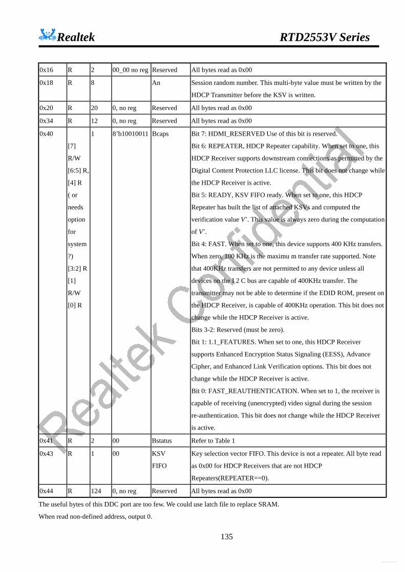
Realtek RTD2553V Series
135
0x16 R 2 00_00 no reg Reserved All bytes read as 0x00
0x18 R 8 An Session random number. This multi-byte value must be written by the
HDCP Transmitter before the KSV is written.
0x20 R 20 0, no reg Reserved All bytes read as 0x00
0x34 R 12 0, no reg Reserved All bytes read as 0x00
0x40
[7]
R/W
[6:5] R,
[4] R
( or
needs
option
for
system
?)
[3:2] R
[1]
R/W
[0] R
1 8’b10010011 Bcaps Bit 7: HDMI_RESERVED Use of this bit is reserved.
Bit 6: REPEATER, HDCP Repeater capability. When set to one, this
HDCP Receiver supports downstream connections as permitted by the
Digital Content Protection LLC license. This bit does not change while
the HDCP Receiver is active.
Bit 5: READY, KSV FIFO ready. When set to one, this HDCP
Repeater has built the list of attached KSVs and computed the
verification value V’. This value is always zero during the computation
of V’.
Bit 4: FAST. When set to one, this device supports 400 KHz transfers.
When zero, 100 KHz is the maximu m transfer rate supported. Note
that 400KHz transfers are not permitted to any device unless all
devices on the I 2 C bus are capable of 400KHz transfer. The
transmitter may not be able to determine if the EDID ROM, present on
the HDCP Receiver, is capable of 400KHz operation. This bit does not
change while the HDCP Receiver is active.
Bits 3-2: Reserved (must be zero).
Bit 1: 1.1_FEATURES. When set to one, this HDCP Receiver
supports Enhanced Encryption Status Signaling (EESS), Advance
Cipher, and Enhanced Link Verification options. This bit does not
change while the HDCP Receiver is active.
Bit 0: FAST_REAUTHENTICATION. When set to 1, the receiver is
capable of receiving (unencrypted) video signal during the session
re-authentication. This bit does not change while the HDCP Receiver
is active.
0x41 R 2 00 Bstatus Refer to Table 1
0x43 R 1 00 KSV
FIFO
Key selection vector FIFO. This device is not a repeater. All byte read
as 0x00 for HDCP Receivers that are not HDCP
Repeaters(REPEATER==0).
0x44 R 124 0, no reg Reserved All bytes read as 0x00
The useful bytes of this DDC port are too few. We could use latch file to replace SRAM.
When read non-defined address, output 0.
http://www.DataSheet4U.net/
datasheet pdf - http://www.DataSheet4U.net/
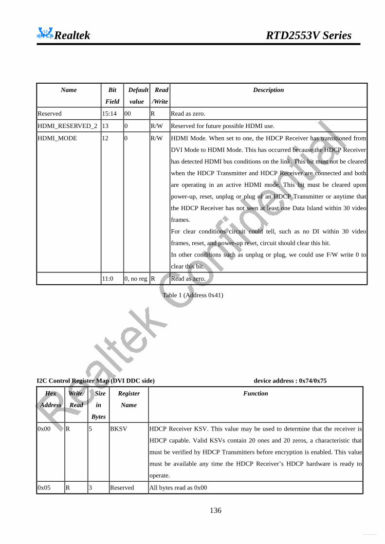
Realtek RTD2553V Series
136
Name Bit
Field
Default
value
Read
/Write
Description
Reserved 15:14 00 R Read as zero.
HDMI_RESERVED_2 13 0 R/W Reserved for future possible HDMI use.
HDMI_MODE 12 0 R/W HDMI Mode. When set to one, the HDCP Receiver has transitioned from
DVI Mode to HDMI Mode. This has occurred because the HDCP Receiver
has detected HDMI bus conditions on the link. This bit must not be cleared
when the HDCP Transmitter and HDCP Receiver are connected and both
are operating in an active HDMI mode. This bit must be cleared upon
power-up, reset, unplug or plug of an HDCP Transmitter or anytime that
the HDCP Receiver has not seen at least one Data Island within 30 video
frames.
For clear conditions circuit could tell, such as no DI within 30 video
frames, reset, and power-up reset, circuit should clear this bit.
In other conditions such as unplug or plug, we could use F/W write 0 to
clear this bit.
11:0 0, no reg R Read as zero.
Table 1 (Address 0x41)
I2C Control Register Map (DVI DDC side) device address : 0x74/0x75
Hex
Address
Write/
Read
Size
in
Bytes
Register
Name
Function
0x00 R 5 BKSV HDCP Receiver KSV. This value may be used to determine that the receiver is
HDCP capable. Valid KSVs contain 20 ones and 20 zeros, a characteristic that
must be verified by HDCP Transmitters before encryption is enabled. This value
must be available any time the HDCP Receiver’s HDCP hardware is ready to
operate.
0x05 R 3 Reserved All bytes read as 0x00
http://www.DataSheet4U.net/
datasheet pdf - http://www.DataSheet4U.net/
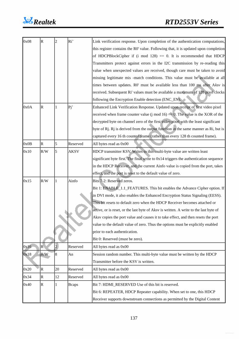
Realtek RTD2553V Series
137
0x08 R 2 Ri’ Link verification response. Upon completion of the authentication computations,
this register contains the R0' value. Following that, it is updated upon completion
of HDCPBlockCipher if (i mod 128) == 0. It is recommended that HDCP
Transmitters protect against errors in the I2C transmission by re-reading this
value when unexpected values are received, though care must be taken to avoid
missing legitimate mis -match conditions. This value must be available at all
times between updates. R0' must be available less than 100 ms after Aksv is
received. Subsequent Ri' values must be available a maximum of 128 pixel clocks
following the Encryption Enable detection (ENC_EN).
0x0A R 1 Pj’ Enhanced Link Verification Response. Updated upon receipt of first video pixel
received when frame counter value (j mod 16) == 0. The value is the XOR of the
decrypted byte on channel zero of the first video pixel with the least significant
byte of Rj. Rj is derived from the output function in the same manner as Ri, but is
captured every 16 th counted frame (rather than every 128 th counted frame).
0x0B R 5 Reserved All bytes read as 0x00
0x10 R/W 5 AKSV HDCP transmitter KSV. Writes to this multi-byte value are written least
significant byte first. The final write to 0x14 triggers the authentication sequence
in the HDCP Receiver, and the current Ainfo value is copied from the port, takes
effect, and the port is reset to the default value of zero.
0x15 R/W 1 Ainfo Bits 7-2: Reserved zeros.
Bit 1: ENABLE_1.1_FEATURES. This bit enables the Advance Cipher option. If
in DVI mode, it also enables the Enhanced Encryption Status Signaling (EESS).
This bit resets to default zero when the HDCP Receiver becomes attached or
active, or is reset, or the last byte of Aksv is written. A write to the last byte of
Aksv copies the port value and causes it to take effect, and then resets the port
value to the default value of zero. Thus the options must be explicitly enabled
prior to each authentication.
Bit 0: Reserved (must be zero).
0x16 R 2 Reserved All bytes read as 0x00
0x18 R/W 8 An Session random number. This multi-byte value must be written by the HDCP
Transmitter before the KSV is written.
0x20 R 20 Reserved All bytes read as 0x00
0x34 R 12 Reserved All bytes read as 0x00
0x40 R 1 Bcaps Bit 7: HDMI_RESERVED Use of this bit is reserved.
Bit 6: REPEATER, HDCP Repeater capability. When set to one, this HDCP
Receiver supports downstream connections as permitted by the Digital Content
http://www.DataSheet4U.net/
datasheet pdf - http://www.DataSheet4U.net/
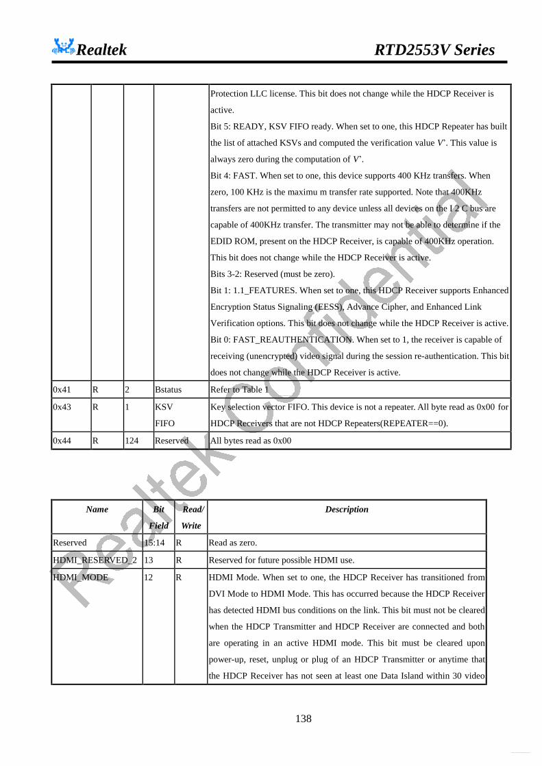
Realtek RTD2553V Series
138
Protection LLC license. This bit does not change while the HDCP Receiver is
active.
Bit 5: READY, KSV FIFO ready. When set to one, this HDCP Repeater has built
the list of attached KSVs and computed the verification value V’. This value is
always zero during the computation of V’.
Bit 4: FAST. When set to one, this device supports 400 KHz transfers. When
zero, 100 KHz is the maximu m transfer rate supported. Note that 400KHz
transfers are not permitted to any device unless all devices on the I 2 C bus are
capable of 400KHz transfer. The transmitter may not be able to determine if the
EDID ROM, present on the HDCP Receiver, is capable of 400KHz operation.
This bit does not change while the HDCP Receiver is active.
Bits 3-2: Reserved (must be zero).
Bit 1: 1.1_FEATURES. When set to one, this HDCP Receiver supports Enhanced
Encryption Status Signaling (EESS), Advance Cipher, and Enhanced Link
Verification options. This bit does not change while the HDCP Receiver is active.
Bit 0: FAST_REAUTHENTICATION. When set to 1, the receiver is capable of
receiving (unencrypted) video signal during the session re-authentication. This bit
does not change while the HDCP Receiver is active.
0x41 R 2 Bstatus Refer to Table 1
0x43 R 1 KSV
FIFO
Key selection vector FIFO. This device is not a repeater. All byte read as 0x00 for
HDCP Receivers that are not HDCP Repeaters(REPEATER==0).
0x44 R 124 Reserved All bytes read as 0x00
Name Bit
Field
Read/
Write
Description
Reserved 15:14 R Read as zero.
HDMI_RESERVED_2 13 R Reserved for future possible HDMI use.
HDMI_MODE 12 R HDMI Mode. When set to one, the HDCP Receiver has transitioned from
DVI Mode to HDMI Mode. This has occurred because the HDCP Receiver
has detected HDMI bus conditions on the link. This bit must not be cleared
when the HDCP Transmitter and HDCP Receiver are connected and both
are operating in an active HDMI mode. This bit must be cleared upon
power-up, reset, unplug or plug of an HDCP Transmitter or anytime that
the HDCP Receiver has not seen at least one Data Island within 30 video
http://www.DataSheet4U.net/
datasheet pdf - http://www.DataSheet4U.net/
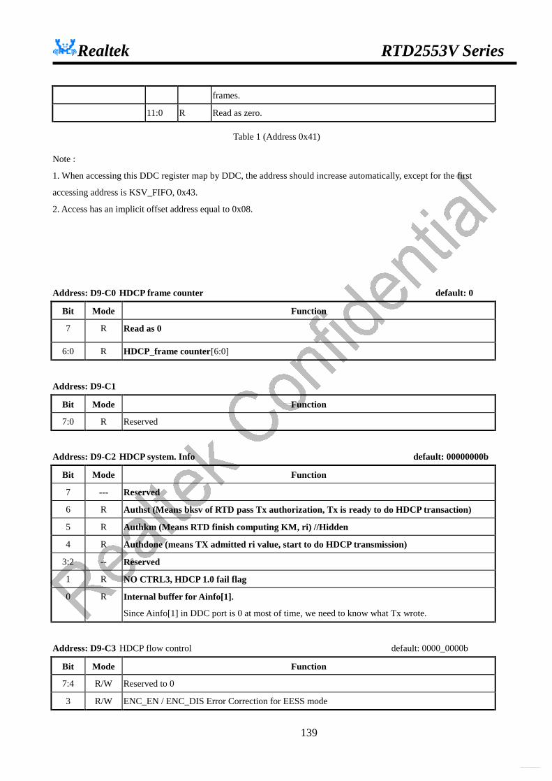
Realtek RTD2553V Series
139
frames.
11:0 R Read as zero.
Table 1 (Address 0x41)
Note :
1. When accessing this DDC register map by DDC, the address should increase automatically, except for the first
accessing address is KSV_FIFO, 0x43.
2. Access has an implicit offset address equal to 0x08.
Address: D9-C0 HDCP frame counter default: 0
Bit Mode Function
7 R Read as 0
6:0 R HDCP_frame counter[6:0]
Address: D9-C1
Bit Mode Function
7:0 R Reserved
Address: D9-C2 HDCP system. Info default: 00000000b
Bit Mode Function
7 --- Reserved
6 R Authst (Means bksv of RTD pass Tx authorization, Tx is ready to do HDCP transaction)
5 R Authkm (Means RTD finish computing KM, ri) //Hidden
4 R Authdone (means TX admitted ri value, start to do HDCP transmission)
3:2 -- Reserved
1 R NO CTRL3, HDCP 1.0 fail flag
0 R Internal buffer for Ainfo[1].
Since Ainfo[1] in DDC port is 0 at most of time, we need to know what Tx wrote.
Address: D9-C3 HDCP flow control default: 0000_0000b
Bit Mode Function
7:4 R/W Reserved to 0
3 R/W ENC_EN / ENC_DIS Error Correction for EESS mode
http://www.DataSheet4U.net/
datasheet pdf - http://www.DataSheet4U.net/
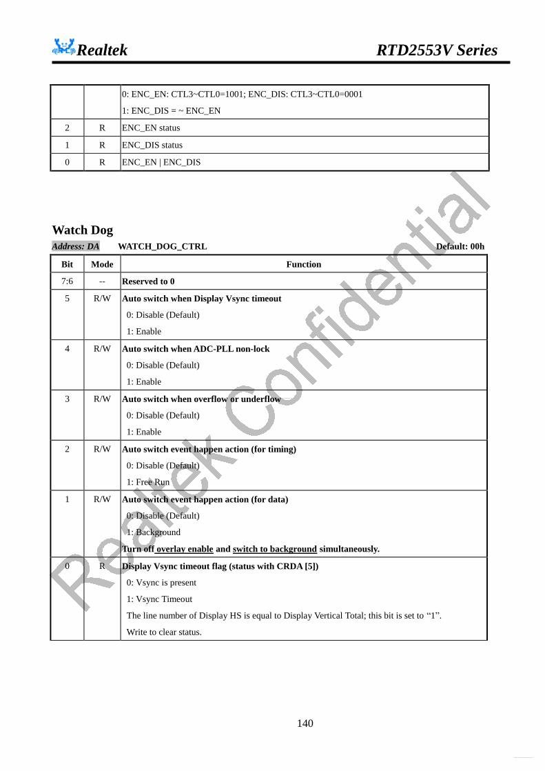
Realtek RTD2553V Series
140
0: ENC_EN: CTL3~CTL0=1001; ENC_DIS: CTL3~CTL0=0001
1: ENC_DIS = ~ ENC_EN
2 R ENC_EN status
1 R ENC_DIS status
0 R ENC_EN | ENC_DIS
Watch Dog Address: DA WATCH_DOG_CTRL Default: 00h
Bit Mode Function
7:6 -- Reserved to 0
5 R/W Auto switch when Display Vsync timeout
0: Disable (Default)
1: Enable
4 R/W Auto switch when ADC-PLL non-lock
0: Disable (Default)
1: Enable
3 R/W Auto switch when overflow or underflow
0: Disable (Default)
1: Enable
2 R/W Auto switch event happen action (for timing)
0: Disable (Default)
1: Free Run
1 R/W Auto switch event happen action (for data)
0: Disable (Default)
1: Background
Turn off overlay enable and switch to background simultaneously.
0 R Display Vsync timeout flag (status with CRDA [5])
0: Vsync is present
1: Vsync Timeout
The line number of Display HS is equal to Display Vertical Total; this bit is set to “1”.
Write to clear status.
http://www.DataSheet4U.net/
datasheet pdf - http://www.DataSheet4U.net/
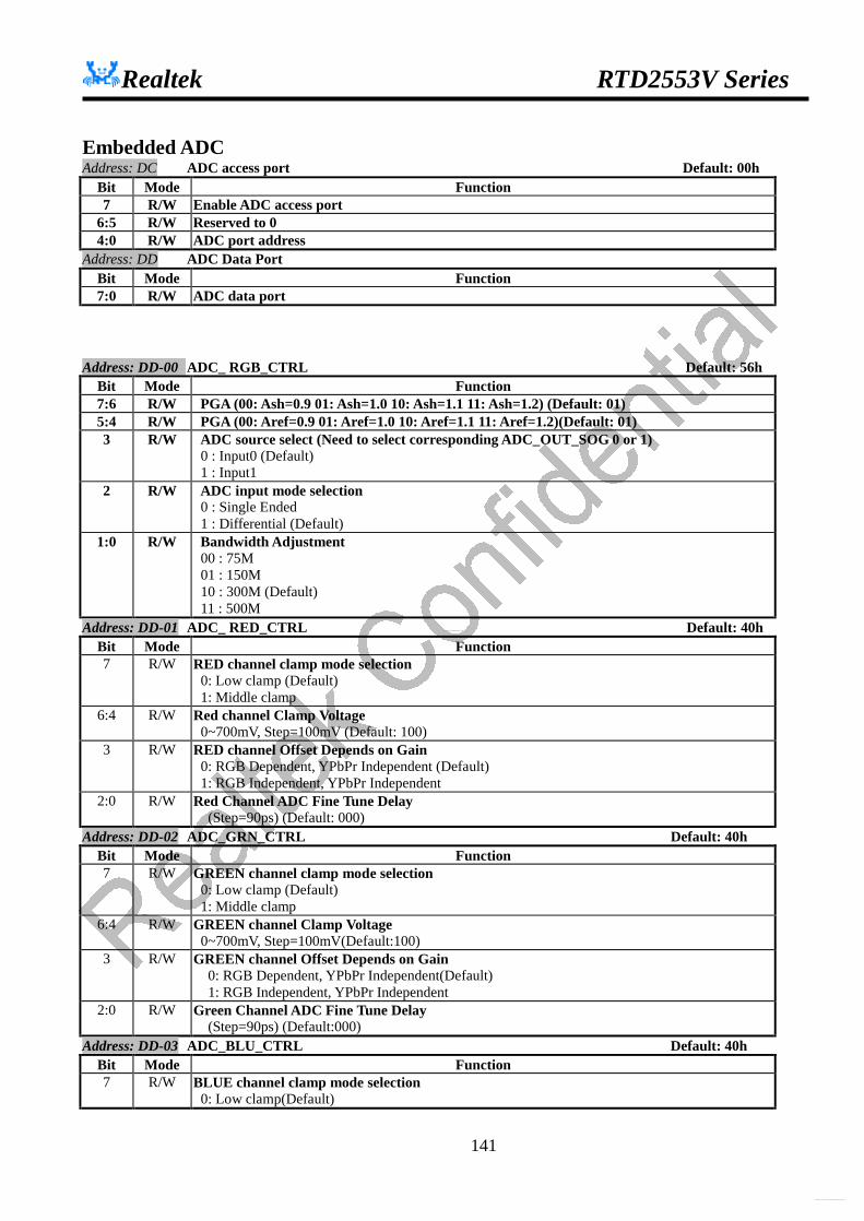
Realtek RTD2553V Series
141
Embedded ADC Address: DC ADC access port Default: 00h
Bit Mode Function 7 R/W Enable ADC access port
6:5 R/W Reserved to 0 4:0 R/W ADC port address
Address: DD ADC Data Port Bit Mode Function 7:0 R/W ADC data port
Address: DD-00 ADC_ RGB_CTRL Default: 56h
Bit Mode Function 7:6 R/W PGA (00: Ash=0.9 01: Ash=1.0 10: Ash=1.1 11: Ash=1.2) (Default: 01) 5:4 R/W PGA (00: Aref=0.9 01: Aref=1.0 10: Aref=1.1 11: Aref=1.2)(Default: 01) 3 R/W ADC source select (Need to select corresponding ADC_OUT_SOG 0 or 1)
0 : Input0 (Default) 1 : Input1
2 R/W ADC input mode selection 0 : Single Ended 1 : Differential (Default)
1:0 R/W Bandwidth Adjustment 00 : 75M 01 : 150M 10 : 300M (Default) 11 : 500M
Address: DD-01 ADC_ RED_CTRL Default: 40h Bit Mode Function 7 R/W RED channel clamp mode selection
0: Low clamp (Default) 1: Middle clamp
6:4 R/W Red channel Clamp Voltage 0~700mV, Step=100mV (Default: 100)
3 R/W RED channel Offset Depends on Gain 0: RGB Dependent, YPbPr Independent (Default)
1: RGB Independent, YPbPr Independent 2:0 R/W Red Channel ADC Fine Tune Delay
(Step=90ps) (Default: 000) Address: DD-02 ADC_GRN_CTRL Default: 40h
Bit Mode Function 7 R/W GREEN channel clamp mode selection
0: Low clamp (Default) 1: Middle clamp
6:4 R/W GREEN channel Clamp Voltage 0~700mV, Step=100mV(Default:100)
3 R/W GREEN channel Offset Depends on Gain 0: RGB Dependent, YPbPr Independent(Default) 1: RGB Independent, YPbPr Independent
2:0 R/W Green Channel ADC Fine Tune Delay (Step=90ps) (Default:000)
Address: DD-03 ADC_BLU_CTRL Default: 40h Bit Mode Function 7 R/W BLUE channel clamp mode selection
0: Low clamp(Default)
http://www.DataSheet4U.net/
datasheet pdf - http://www.DataSheet4U.net/
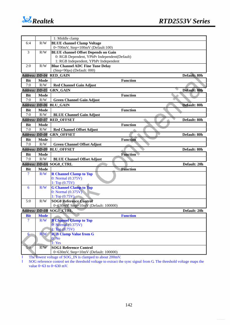
Realtek RTD2553V Series
142
1: Middle clamp 6:4 R/W BLUE channel Clamp Voltage
0~700mV, Step=100mV (Default:100) 3 R/W BLUE channel Offset Depends on Gain
0: RGB Dependent, YPbPr Independent(Default) 1: RGB Independent, YPbPr Independent
2:0 R/W Blue Channel ADC Fine Tune Delay (Step=90ps) (Default: 000)
Address: DD-04 RED_GAIN Default: 80h Bit Mode Function 7:0 R/W Red Channel Gain Adjust
Address: DD-05 GRN_GAIN Default: 80h Bit Mode Function 7:0 R/W Green Channel Gain Adjust
Address: DD-06 BLU_GAIN Default: 80h Bit Mode Function 7:0 R/W BLUE Channel Gain Adjust
Address: DD-07 RED_OFFSET Default: 80h Bit Mode Function 7:0 R/W Red Channel Offset Adjust
Address: DD-08 GRN_OFFSET Default: 80h Bit Mode Function 7:0 R/W Green Channel Offset Adjust
Address: DD-09 BLU_OFFSET Default: 80h Bit Mode Function 7:0 R/W BLUE Channel Offset Adjust
Address: DD-0A SOG0_CTRL Default: 20h Bit Mode Function 7 R/W R Channel Clamp to Top
0: Normal (0.375V) 1: Top (0.75V)
6 R/W G Channel Clamp to Top 0: Normal (0.375V) 1: Top (0.75V)
5:0 R/W SOG0 Reference Control 0~630mV, Step=10mV (Default: 100000)
Address: DD-0B SOG1_CTRL Default: 20h Bit Mode Function 7 R/W B Channel Clamp to Top
0: Normal (0.375V) 1: Top (0.75V)
6 R/W R, B Clamp Value from G 0: No 1: Yes
5:0 R/W SOG1 Reference Control 0~630mV, Step=10mV (Default: 100000)
l The lowest voltage of SOG_IN is clamped to about 200mV. l SOG reference control set the threshold voltage to extract the sync signal from G. The threshold voltage maps the
value 0~63 to 0~630 mV.
http://www.DataSheet4U.net/
datasheet pdf - http://www.DataSheet4U.net/

Realtek RTD2553V Series
143
SOG_IN SOG_ShiftLevel_Shift
SOG_Compare
(Minimum Voltage at 200mV)
(Compare 0~630mV, step 10mV)Capacitor
0V
-300mV0V
200mV
500mVCompare Voltage(0~630mV)
Address: DD-0C ADC_POWER_CTRL Default: 08h
Bit Mode Function 7 R/W SOG Mode
0: NMOS/R 1: Clamping
6 R/W SOG Channel Clamp to –300mV 0: 500mV 1: 200mV
5 R/W SOG0 Power On 0 : Power Down(Default) 1 : Power On
4 R/W SOG1 Power On 0 : Power Down(Default) 1 : Power On
3 R/W Band-gap Power On 0 : Power Down 1 : Power On (Default)
2 R/W Red Channel ADC Power On 0 : Power Down (Default) 1 : Power On
1 R/W Green Channel ADC Power On 0 : Power Down (Default) 1 : Power On
0 R/W Blue Channel ADC Power On 0 : Power Down (Default) 1 : Power On
l Note that Band-gap power can only turn off just in the power down mode, or the chip may run abnormally. l When in power saving mode, only R/G/B channel will be power down, it doesn’t include the SOG & band-gap. Address: DD-0D ADC_CLOCK Default: 01h
Bit Mode Function 7 R/W Input Clock Polarity
0: Negative (Default) 1: Positive
6 R/W Output Clock Polarity 0: Normal (Default) 1: Inverted
5:4 R/W ADC_Out Pixel Extra Delay 00: 1.05ns (Default) 01: 1.39ns 10: 1.69ns 11: 1.97ns
http://www.DataSheet4U.net/
datasheet pdf - http://www.DataSheet4U.net/

Realtek RTD2553V Series
144
3 R/W 1x or 2x from APLL (For better clock duty cycle) 0: 1X (Default) 1: 2X
2 R/W Single Ended or Differential clock from APLL 0: Differential (Default) 1: Single Ended
1:0 R/W Duty Stablizer (Default: 01) Address: DD-0E ADC_TEST Default: 04h
Bit Mode Function 7 R/W Reserved to 0
6:4 R/W Test Output Selection (PAD : SOGIN0/SOGIN1)
000:X/X(Hi-Z) Normal SOG Mode (Default)
001:GND/GND
010:VRBIR/VREFN
011:VCMI/VCMO
100:VRTIR/VREFP
101:VMID/GND
110:VOFFSET/GND
111:VDD/VDD 3:2 R/W SOG Resistor
00: open
01: Poly R=500K, external C=10nf (Default)
10: MOS R=1M, external C=4.7nF
11: MOS R=5M, external C=1nF 1:0 R/W Clock Output Divider
00 : 1/1 (Default) 01 : 1/2 10 : 1/3 11 : 1/4
Address: DD-0F ADC_IBIAS2 Default: 53h Bit Mode Function 7:6 R/W APLL_IB60U[1:0]
Bias Current of APLL_IB60U 00:48u
01:60u (Default) 10:72u
11:84u 5:4 R/W ADC_SF[1:0]
Bias Current of ADC_SF 00:15u
01:20u (Default) 10:25u 11:30u
3 R/W ADC_REF Bias Current of ADC_REF
0:60u (Default) 1:80u
http://www.DataSheet4U.net/
datasheet pdf - http://www.DataSheet4U.net/
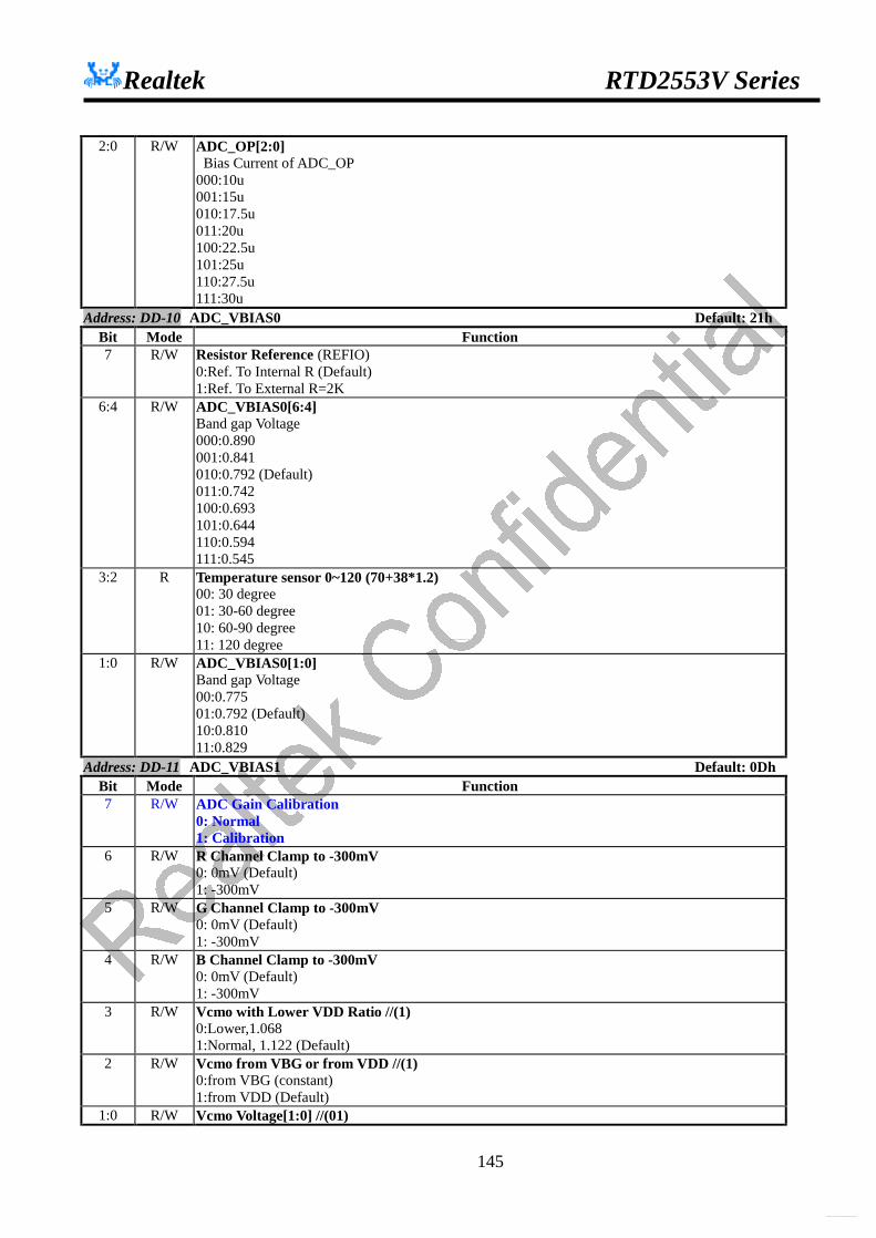
Realtek RTD2553V Series
145
2:0 R/W ADC_OP[2:0] Bias Current of ADC_OP 000:10u 001:15u 010:17.5u 011:20u 100:22.5u 101:25u 110:27.5u 111:30u
Address: DD-10 ADC_VBIAS0 Default: 21h Bit Mode Function 7 R/W Resistor Reference (REFIO)
0:Ref. To Internal R (Default) 1:Ref. To External R=2K
6:4 R/W ADC_VBIAS0[6:4] Band gap Voltage 000:0.890 001:0.841 010:0.792 (Default) 011:0.742 100:0.693 101:0.644 110:0.594 111:0.545
3:2 R Temperature sensor 0~120 (70+38*1.2) 00: 30 degree 01: 30-60 degree 10: 60-90 degree 11: 120 degree
1:0 R/W ADC_VBIAS0[1:0] Band gap Voltage 00:0.775 01:0.792 (Default) 10:0.810 11:0.829
Address: DD-11 ADC_VBIAS1 Default: 0Dh Bit Mode Function 7 R/W ADC Gain Calibration
0: Normal 1: Calibration
6 R/W R Channel Clamp to -300mV 0: 0mV (Default) 1: -300mV
5 R/W G Channel Clamp to -300mV 0: 0mV (Default) 1: -300mV
4 R/W B Channel Clamp to -300mV 0: 0mV (Default) 1: -300mV
3 R/W Vcmo with Lower VDD Ratio //(1) 0:Lower,1.068 1:Normal, 1.122 (Default)
2 R/W Vcmo from VBG or from VDD //(1) 0:from VBG (constant) 1:from VDD (Default)
1:0 R/W Vcmo Voltage[1:0] //(01)
http://www.DataSheet4U.net/
datasheet pdf - http://www.DataSheet4U.net/
Realtek RTD2553V Series
146
00:0.90 01:1.00 (Default) 11:1.05 11:1.10
Address: DD-12 PTNPOS_H Default: 00h
Bit Mode Function
7 R/W Enable Test
0: Finish (and result sequence is R-G-B) (Default)
1: Start
6:4 R/W Test Pattern V Position Register [10:8]
Assign the test pattern digitized position in line after V_Start.
3 -- Reserved to 0
2:0 R/W Test Pattern H Position Register [10:8]
Assign the test pattern digitized position in pixel after H_Start.
Address: DD-13 PTNPOS_V_L
Bit Mode Function
7:0 R/W Test Pattern V Position Register [7:0] Assign the test pattern digitized position in line after V_Start..
Address: DD-14 PTNPOS_H_L
Bit Mode Function
7:0 R/W Test Pattern H Position Register [7:0] Assign the test pattern digitized position in line after H_Start..
Use PTNPOS to assign the pixel position after HSYNC leading edge that input signal digitized. Each time the
PTNPOS is written, the digitized results will be loaded into PTNRD, PTNGD and PTNBD. For test issue, make the
input signal a fixed pattern before PTNPOS is written. Then the same digitized output will be got.
Address: DD-15 PTNRD
Bit Mode Function
7:0 R Test Pattern Red-Channel Digitized Result.
Address: DD-16 PTNRD
Bit Mode Function
7:0 R Test Pattern Green-Channel Digitized Result.
Address: DD-17 PTNRD
Bit Mode Function
7:0 R Test Pattern Blue-Channel Digitized Result.
l The test pattern digitized result after HSYNC leading edge about PTNPOS pixel.
http://www.DataSheet4U.net/
datasheet pdf - http://www.DataSheet4U.net/
Realtek RTD2553V Series
147
ICM Address: E0 ICM Control Default: 00h
Bit Mode Function 7 R/W ICM Enable
0: Disable 1: Enable
6 R/W Y Correction 0: Disable 1: Enable
5 R/W Reserved to 0 4 R/W CM0 Enable
0: Disable 1: Enable
3 R/W CM1 Enable 0: Disable 1: Enable
2 R/W CM2 Enable 0: Disable 1: Enable
1 R/W CM3 Enable 0: Disable 1: Enable
0 R/W CM4 Enable 0: Disable 1: Enable
Address:E1 ICM_SEL Default: 00h
Bit Mode Function 7:5 R/W ICM Test Mode
000: disable 001: bypass U, V result 010: bypass hue/saturation result 011: bypass dU, dV value 1xx: R,B as LUT input, and bypass LUT output to R/G/B output
4:3 -- reserved 2:0 R/W CM Select
000: Select Chroma Modifier 0 for Accessing Through Data Port 001: Select Chroma Modifier 1 for Accessing Through Data Port 010: Select Chroma Modifier 2 for Accessing Through Data Port 011: Select Chroma Modifier 3 for Accessing Through Data Port 100: Select Chroma Modifier 4 for Accessing Through Data Port 101~111: reserved
Address:E2 ICM_ADDR Default: 00h
Bit Mode Function 7:0 R/W ICM port address
Address:E3 ICM_Data Bit Mode Function 7:0 R/W ICM port data
ICM_ADDR will be increased automatically after each byte of ICM_DATA has been accessed.
Address: E3-00 MST_HUE_HB Default: x0h
Bit Mode Function 7:4 -- Reserved
http://www.DataSheet4U.net/
datasheet pdf - http://www.DataSheet4U.net/

Realtek RTD2553V Series
148
3:0 W High Byte[11:8] of Master Hue for Chroma Modifier N. Address: E3-01 MST_HUE_LB Default: 00h
Bit Mode Function 7:0 W Low Byte[7:0] of Master Hue for Chroma Modifier N.
Address: E3-02 HUE_SET Default: 00h Bit Mode Function 7:6 W CM[N]_LWID
00: CM[N] left width 0 01: CM[N] left width 1 10: CM[N] left width 2 11: CM[N] left width 3
5:4 W CM[N]_LBUF 00: CM[N] left Buffer 0 01: CM[N] left Buffer 1 10: CM[N] left Buffer 2 11: CM[N] left Buffer 3
3:2 W CM[N]_RWID 00: CM[N] right width 0 01: CM[N] right width 1 10: CM[N] right width 2 11: CM[N] right width 3
1:0 W CM[N]_RBUF 00: CM[N] right Buffer 0 01: CM[N] right Buffer 1 10: CM[N] right Buffer 2 11: CM[N] right Buffer 3
Address: E3-03~32 U/V Offset Default: 00h
Bit Mode Function 7:0 W Addr 03: U Offset 00,
Addr 04: V Offset 00, Addr 05: U Offset 01, Addr 06: V Offset 01, Addr 07: U Offset 02, Addr 08: V Offset 02, Addr 09: U Offset 03, Addr 0A: V Offset 03, Addr 0B: U Offset 04, Addr 0C: V Offset 04, Addr 0D: U Offset 05, Addr 0E: V Offset 05, Addr 0F: U Offset 06, Addr 10: V Offset 06, Addr 11: U Offset 07, Addr 12: V Offset 07, Addr 13: U Offset 10, Addr 14: V Offset 10, Addr 15: U Offset 11, Addr 16: V Offset 11, Addr 17: U Offset 12, Addr 18: V Offset 12, Addr 19: U Offset 13, Addr 1A: V Offset 13, Addr 1B: U Offset 14, Addr 1C: V Offset 14,
http://www.DataSheet4U.net/
datasheet pdf - http://www.DataSheet4U.net/

Realtek RTD2553V Series
149
Addr 1D: U Offset 15, Addr 1E: V Offset 15, Addr 1F: U Offset 16, Addr 20: V Offset 16, Addr 21: U Offset 17, Addr 22: V Offset 17, Addr 23: U Offset 20, Addr 24: V Offset 20, Addr 25: U Offset 21, Addr 26: V Offset 21, Addr 27: U Offset 22, Addr 28: V Offset 22, Addr 29: U Offset 23, Addr 2A: V Offset 23, Addr 2B: U Offset 24, Addr 2C: V Offset 24, Addr 2D: U Offset 25, Addr 2E: V Offset 25, Addr 2F: U Offset 26, Addr 30: V Offset 26, Addr 31: U Offset 27, Addr 32: V Offset 27,
DCC Address: E4 DCC_CTRL0 Default: 00h
Bit Mode Function 7 R/W DCC_ENABLE
0: Disable 1: Enable
6 R/W Y_FORMULA 0: Formula 0 1: Formula 1
5 R/W SOFT_CLAMP 0: Disable 1: Enable
4 R/W DCC_MODE 0: Auto Mode
Offset 07
Offset 17
Offset 10
Offset 27
Offset 20 Offset 00
http://www.DataSheet4U.net/
datasheet pdf - http://www.DataSheet4U.net/

Realtek RTD2553V Series
150
1: Manual Mode 3 R/W SCENE_CHANGE
0: Disable Scene-Change Function 1: Enable Scene-Change Function in Auto Mode
2 R/W BWL_EXP 0: Disable Black/White Level Expansion 1: Enable Black/White Level Expansion in Auto Mode
1:0 R/W DCC_PAGE_SEL 00: Page 0 (for Histogram / Ymin-max / Soft-Clamping / Scene-Change) 01: Page 1 (for Y-Curve / WBL Expansion) 10: Page 2 (for Calculation Parameter) 11: Page 3 (for Testing and Debug)
Address: E5 DCC_CTRL1 Default: 00h
Bit Mode Function 7 R/W DCC gain control enable
0: Disable 1: Enable Note: DCC gain control enable must delay MOV_AVG_LEN frame after DCC enable.
6 R 1: time to write highlight window position & normalized factor, write to clear 5:0 -- Reserved 0
Address: E6 DCC Address Port
Bit Mode Function 7:0 R/W DCC Address
Address: E7 DCC Data Port
Bit Mode Function 7:0 R/W DCC Data
DCC_ADDR will be increased automatically after each byte of DCC_DATA has been accessed.
Address: E7-00 (page0) NOR_FACTOR_H
Bit Mode Function 7:6 -- Reserved 5:0 R/W Bit[21:16] of Normalized Factor; NF=(255/N)*(2^22)
Address: E7-01 (page0) NOR_FACTOR_M Bit Mode Function 7:0 R/W Bit[15:8] of Normalized Factor; NF=(255/N)*(2^22)
Address: E7-02 (page0) NOR_FACTOR_L Bit Mode Function 7:0 R/W Bit[7:0] of Normalized Factor; NF=(255/N)*(2^22)
Address: E7-03 (page0) BBE_CTRL default: 04h
Bit Mode Function 7 R/W BBE_ENA
0: Disable Black-Background Exception 1: Enable Black-Background Exception
6:4 -- Reserved 3:0 R/W BBE_THD
http://www.DataSheet4U.net/
datasheet pdf - http://www.DataSheet4U.net/
Realtek RTD2553V Series
151
8-bit RGB Threshold for Black-Background Exception
Address: E7-04 (page0) NFLT_CTRL default: 00h
Bit Mode Function 7 R/W HNFLT_ENA
0: Disable Histogram Noise Filter 1: Enable Histogram Noise Filter
6:4 R/W HNFLT_THD Threshold for Histogram Noise Filter
3 R/W YNFLT_ENA 0: Disable Ymax / Ymin Noise Filter 1: Enable Ymax / Ymin Noise Filter
2:0 R/W YNFLT_THD Threshold for Ymax/Ymin Noise Filter (= 4*YNFLT_THD)
Address: E7-05 (page0) HIST_CTRL default: 00h
Bit Mode Function 7 R/W RH0_LIMITER
0: Disable RH0 Limiter 1: Enable RH0 Limiter
6 R/W RH1_LIMITER 0: Disable RH1 Limiter 1: Enable RH1 Limiter
5:3 -- Reserved 2:0 R/W MOV_AVG_LEN
000: Histogram Moving Average Length = 1 001: Histogram Moving Average Length = 2 010: Histogram Moving Average Length = 4 011: Histogram Moving Average Length = 8 100: Histogram Moving Average Length = 16 101~111: reserved
Address: E7-06 (page0) SOFT_CLAMP default: B0h
Bit Mode Function 7:0 R/W Slope of Soft-Clamping (= SOFT_CLAMP / 256)
Address: E7-07 (page0) Y_MAX_LB default: FFh
Bit Mode Function 7:0 R/W Lower Bound of Y_MAX (= 4*Y_MAX_LB)
Address: E7-08 (page0) Y_MIN_HB default: 00h Bit Mode Function 7:0 R/W Higher Bound of Y_MIN (= 4*Y_MIN_HB)
Address: E7-09 (page0) SCG_PERIOD default: xxx10000b
Bit Mode Function 7:5 -- Reserved 4:0 R/W Scene-Change Mode Period = 1~32.
Note: SCG_PERIOD >= MOV_AVG_LEN, CRE7-05[2:0](page0) Address: E7-0A (page0) SCG_LB default: 00h
Bit Mode Function 7:0 R/W SCG_DIFF Lower Bound for Exiting Scene-Change Mode
Address: E7-0B (page0) SCG_HB default: FFh
http://www.DataSheet4U.net/
datasheet pdf - http://www.DataSheet4U.net/
Realtek RTD2553V Series
152
Bit Mode Function 7:0 R/W SCG_DIFF Higher Bound for Exiting Scene-Change Mode
Address: E7-0C (page0) POPUP_CTRL Bit Mode Function 7:1 Reserved 0 R Reg[0D]~Reg[16] are updated every frame. Once POPUP_BIT is read, the value of Reg[0D] ~
Reg[16] will not be updated until Reg[16] is read. Address: E7-0D (page0) SCG_DIFF
Bit Mode Function 7:0 R = (Histogram Difference between Current Frame and Average) / 8
Address: E7-0E (page0) Y_MAX_VAL
Bit Mode Function 7:0 R = Max { Y_MAX_LB, (Y Maximum in Current Frame / 4) }
Address: E7-0F (page0) Y_MIN_VAL Bit Mode Function 7:0 R = Min { Y_MIN_HB, (Y Minimum in Current Frame / 4) }
Address: E7-10 (page0) S0_VALUE
Bit Mode Function 7:0 R Normalized Histogram S0 Value
Address: E7-11 (page0) S1_VALUE Bit Mode Function 7:0 R Normalized Histogram S1 Value
Address: E7-12 (page0) S2_VALUE Bit Mode Function 7:0 R Normalized Histogram S2 Value
Address: E7-13 (page0) S3_VALUE Bit Mode Function 7:0 R Normalized Histogram S3 Value
Address: E7-14 (page0) S4_VALUE Bit Mode Function 7:0 R Normalized Histogram S4 Value
Address: E7-15 (page0) S5_VALUE Bit Mode Function 7:0 R Normalized Histogram S5 Value
Address: E7-16 (page0) S6_VALUE Bit Mode Function 7:0 R Normalized Histogram S6 Value
Address: E7-00 (page1) DEF_CRV[01] default:10h
Bit Mode Function 7:0 R/W Pre-Defined Y-Curve; Keep DEF_CRV[N] ≥ DEF_CRV[N-1]
Address: E7-01 (page1) DEF_CRV[02] default:20h Bit Mode Function 7:0 R/W Pre-Defined Y-Curve; Keep DEF_CRV[N] ≥ DEF_CRV[N-1]
Address: E7-02 (page1) DEF_CRV[03] default:30h Bit Mode Function
http://www.DataSheet4U.net/
datasheet pdf - http://www.DataSheet4U.net/

Realtek RTD2553V Series
153
7:0 R/W Pre-Defined Y-Curve; Keep DEF_CRV[N] ≥ DEF_CRV[N-1] Address: E7-03 (page1) DEF_CRV[04] default:40h
Bit Mode Function 7:0 R/W Pre-Defined Y-Curve; Keep DEF_CRV[N] ≥ DEF_CRV[N-1]
Address: E7-04 (page1) DEF_CRV[05] default:50h Bit Mode Function 7:0 R/W Pre-Defined Y-Curve; Keep DEF_CRV[N] ≥ DEF_CRV[N-1]
Address: E7-05 (page1) DEF_CRV[06] default:60h Bit Mode Function 7:0 R/W Pre-Defined Y-Curve; Keep DEF_CRV[N] ≥ DEF_CRV[N-1]
Address: E7-06 (page1) DEF_CRV[07] default:70h Bit Mode Function 7:0 R/W Pre-Defined Y-Curve; Keep DEF_CRV[N] ≥ DEF_CRV[N-1]
Address: E7-07 (page1) DEF_CRV[08] default:80h Bit Mode Function 7:0 R/W Pre-Defined Y-Curve; Keep DEF_CRV[N] ≥ DEF_CRV[N-1]
Address: E7-08 (page1) DEF_CRV[09] default:90h Bit Mode Function 7:0 R/W Pre-Defined Y-Curve; Keep DEF_CRV[N] ≥ DEF_CRV[N-1]
Address: E7-09 (page1) DEF_CRV[10] default:A0h Bit Mode Function 7:0 R/W Pre-Defined Y-Curve; Keep DEF_CRV[N] ≥ DEF_CRV[N-1]
Address: E7-0A (page1) DEF_CRV[11] default:B0h Bit Mode Function 7:0 R/W Pre-Defined Y-Curve; Keep DEF_CRV[N] ≥ DEF_CRV[N-1]
Address: E7-0B (page1) DEF_CRV[12] default:C0h Bit Mode Function 7:0 R/W Pre-Defined Y-Curve; Keep DEF_CRV[N] ≥ DEF_CRV[N-1]
Address: E7-0C (page1) DEF_CRV[13] default:D0h Bit Mode Function 7:0 R/W Pre-Defined Y-Curve; Keep DEF_CRV[N] ≥ DEF_CRV[N-1]
Address: E7-0D (page1) DEF_CRV[14] default:E0h Bit Mode Function 7:0 R/W Pre-Defined Y-Curve; Keep DEF_CRV[N] ≥ DEF_CRV[N-1]
Address: E7-0E (page1) DEF_CRV[15] default:F0h Bit Mode Function 7:0 R/W Pre-Defined Y-Curve; Keep DEF_CRV[N] ≥ DEF_CRV[N-1]
Registers below is effective only when auto mode is disable and black/white level expansion is enabled.
When auto mode is enabled (DCC_MODE=0), Y_BL_BIAS and Y_WL_BIAS are read-only. Address: E7-0F (page1) Y_BL_BIAS default:00h
Bit Mode Function 7:0 R/W Y Offset for Black-Level Expansion (Y_L' = 4*Y_BL_BIAS)
Address: E7-10 (page1) Y_WL_BIAS default:00h Bit Mode Function 7:0 R/W Y Offset for While-Level Expansion ( 1023-Y_H' = 4*Y_WL_BIAS)
Load double buffer CRE7-00 ~ CRE7-10 (page1) after write CRE7-10 when DCC enable
Registers below is effective only when auto mode is enabled.
In manual mode (DCC_MODE=1), BLD_VAL will be fixed to 0. It means Y-curve is fully determined by
http://www.DataSheet4U.net/
datasheet pdf - http://www.DataSheet4U.net/
Realtek RTD2553V Series
154
DEF_CUR[01~15] Address: E7-11 (page1) BLD_UB default:00h
Bit Mode Function 7:0 R/W Upper Bound of Blending Factor
Address: E7-12 (page1) BLD_LB default:00h Bit Mode Function 7:0 R/W Lower Bound of Blending Factor
Address: E7-13 (page1) DEV_FACTOR default:00h Bit Mode Function 7:0 R/W Deviation Weighting Factor
Address: E7-14 (page1) BLD_VAL Bit Mode Function 7:0 R Blending Value
Address: E7-15 (page1) DEV_VAL_HI Bit Mode Function 7:0 R Bit[8:1] of Deviation Value
Address: E7-16 (page1) DEV_VAL_LO Bit Mode Function 7 R Bit[0] of Deviation Value
6:0 -- Reserved
Address: E7-00~8F (page2) SRAM initial value
Bit Mode Function 7:0 W Hidden
Address: E7-00 (page3) SRAM_BIST default: 00h
Bit Mode Function 7 R/W BIST_EN
0: disable 1: enable
6 R/W RAM_Mode 0: dclk domain mode (normal mode, BIST) 1: MCU domain mode (SCG test)
5:2 -- Reserved 1 R BIST_Period
0: BIST is done 1: BIST is running
0 R BIST_OK 0: SRAM fail 1: SRAM ok
Cyclic-Redundant-Check Address: F2 OP_CRC_CTRL (Output CRC Control Register) Default: 00h
Bit Mode Function
7:1 -- Reserved to 0
http://www.DataSheet4U.net/
datasheet pdf - http://www.DataSheet4U.net/

Realtek RTD2553V Series
155
0 R/W Output CRC Control:
0: Stop or finish (Auto-stop after checked a completed display frame) (Default)
1: Start
CRC function = X^24 + X^7 + X^2 + X + 1.
Address: F3 OP _CRC_CHECKSUM (Output CRC Checksum)
Bit Mode Function
7:0 R/W 1st read=> Output CRC-24 bit 23~16
2nd read=> Output CRC-24 bit 15~8
3rd read=> Out put CRC-24 bit 7~0
l The read pointer should be reset when 1. OP_CRC_BYTE is written 2. Output CRC Control starts.
l The read back CRC value address should be auto-increase, the sequence is shown above
http://www.DataSheet4U.net/
datasheet pdf - http://www.DataSheet4U.net/

Realtek RTD2553V Series
156
DDC Special Function Access (DDC/CI) Address: F4 DDC_SET_SLAVE Default: 6E
Bit Mode Function
7:1 R/W DDC Slave Address to decode
0 -- Reserved to 0
Address: F5 DDC_SUB_IN
Bit Mode Function
7:0 R DDC Sub-Address Received
Address: F6 DDC_DATA_IN
Bit Mode Function
7:0 R/W Read: DDC Data Received (16-bytes buffer)
Write: DDC Data Received (16-bytes buffer)
Every Read/Write access, the buffer index is auto-decreased/increased. Address: F7 DDC_CTRL Default: 00h
Bit Mode Function
7 R/W Start BIST function for DDC SRAM
0: finished and clear
1: start
6 R Test result about DVI DDC SRAM
0: fail
1: ok
5 R Test result about ADC DDC SRAM
0: fail
1: ok
4 -- Reserved
3 R/W Auto reset DDC_DATA Buffer
0: disable
1: enable
In host (pc) write enable, when DDC write (No START after DDC_SUB), reset DDC_DATA
buffer.
2 R/W Reset DDC_DATA buffer
0: Finish
1: Reset
1 R/W DDC_DATA buffer write enable
0: host (pc) write enable
http://www.DataSheet4U.net/
datasheet pdf - http://www.DataSheet4U.net/
Realtek RTD2553V Series
157
1: slave (mcu) write enable
Both PC and MCU can read DDC_DATA buffer, but only one can write DDC_DATA buffer.
0 R/W Channel Select
0: from ADC DDC
1: from DVI DDC
Address: F8 DDC_STATUS
Bit Mode Function
7 R DDC_DATA_BUFFER Full
If DDC_DATA buffer is full, this bit is set to “1”. (On-line monitor)
The DDC_DATA buffer Full status will be on-line-monitor the condition, once it
becomes full, it kept high, if it is not-full, then it goes low.
6 R DDC_DATA_BUFFER Empty
If DDC_DATA buffer is empty, this bit is set to “1”. (On-line monitor)
The DDC_DATA buffer Empty status will be on-line-monitor the condition, once it
becomes empty, it kept high, if it is not-empty, then it goes low.
5 -- Reserved to 0
4 R If DDC_STOP signal occurs, this bit is set to “1” . Write clear.
3 R If DDC_DATA_OUT loaded to serial-out-byte, this bit is set to “1”. Write clear
2 R If DDC_DATA_IN latched, this bit is set to “1” . Write clear
1 R If DDC_SUB latched, this bit is set to “1” Write clear
0 R If DDC_SLAVE latched, this bit is set to “1” Write clear
When DDC Start, clear DDC_Stop flag, CRF8[4].
Address: F9 DDC_IRQ_CTRL Default: 00h
Bit Mode Function
7 R/W 0: Disable the DDC_DATA_BUFFER Full signal as an interrupt source
1: Enable the DDC_DATA_BUFFER Full signal as an interrupt source
6 R/W 0: Disable the DDC_DATA_BUFFER Empty signal as an interrupt source
1: Enable the DDC_DATA_BUFFER Empty signal as an interrupt source
5 --- Reserved
4 R/W 0: Disable the DDC_STOP signal as an interrupt source
1: Enable the DDC_STOP signal as an interrupt source
3 R/W 0: Disable the DDC_DATA_OUT loaded to serial-out-byte as an interrupt source
1: Enable the DDC_DATA_OUT loaded to serial-out-byte as an interrupt source
2 R/W 0: Disable the DDC_DATA_IN latched as an interrupt source
1: Enable the DDC_DATA_IN latched as an interrupt source
1 R/W 0: Disable the DDC_SUB latched as an interrupt source
http://www.DataSheet4U.net/
datasheet pdf - http://www.DataSheet4U.net/

Realtek RTD2553V Series
158
1: Enable the DDC_SUB latched as an interrupt source
0 R/W 0: Disable the DDC_SLAVE latched as an interrupt source
1: Enable the DDC_SLAVE latched as an interrupt source
h t t p : / /www.Da taShee t4U .ne t /
da tashee t pd f - h t t p : / /www.Da taShee t4U .ne t /
Realtek RTD2553V Series
159
DDC Channel (ADC/DVI) (Refers to the VESA “Display Data Channel Standard” for detailed)
Address: FA DDC_ENABLE (DDC Channel Enable Register) Default: 00h
Bit Mode Function
7:5 R/W DDC Channel Address Least Significant 3 Bits
(The default DDC channel address MSB 4 Bits is “A”)
4 R/W DDC Write Status (for external DDC access only)
It is cleared after write.
3 R/W DDC SRAM Write Enable (for external DDC access only)
0: Disable
1: Enable
2 R/W DDC De-bounce Enable
0: Disable
1: Enable (with crystal/4)
1 R/W DDC Channel RAM Size
0: 128 bytes
1: 256 bytes
0 R/W DDC Channel Enable Bit
0: MCU access Enable
1: DDC channel Enable
Address: FB DDC_INDEX (DDC SRAM R/W Index Register)
Bit Mode Function
7:0 R/W DDC SRAM Read/Write Index Register [7:0]
The DDC channel index register will be auto increased one by one after each read or write cycle.
Address: FC DDC_ACCESS_PORT (DDC Channel ACCESS Port)
Bit Mode Function
7:0 R/W DDC SRAM Read/Write Port
** The DDC function can still work when Power_Down & Power_Save.
** After reset, the register will be set to default value, but the SRAM will keep original data. Address: FD DDC_DVI_ENABLE (DDC Channel Enable Register) Default: 00h
Bit Mode Function 7:5 R/W DVI DDC Channel Address Least Significant 3 Bits
(The default DDC channel address MSB 4 Bits is “A”)
4 R DVI DDC External Write Status (for external DDC access only)
It is cleared after write.
3 R/W DVI DDC External Write Enable (for external DDC access only)
0: Disable
http://www.DataSheet4U.net/
datasheet pdf - http://www.DataSheet4U.net/
Realtek RTD2553V Series
160
1: Enable
2 R/W DVI DDC Debounce Enable
0: Disable
1: Enable (with crystal/4)
1 R/W DVI DDC Channel RAM Size
0: 128 bytes
1: 256 bytes 0 R/W DVI DDC Channel Enable Switch
0: MCU access Enable
1: External DDC access Enable Address: FE DDC_DVI_INDEX (DDC SRAM R/W Index Register)
Bit Mode Function 7:0 R/W DVI DDC SRAM Read/Write Index Register [7:0]
l The DDC channel index register will be auto increased one by one after each read or write cycle. Address: FF DDC_DVI_ACCESS_PORT (DDC Channel ACCESS Port)
Bit Mode Function 7:0 R/W DVI DDC SRAM Read/Write Port
l The DDC function can still work when Power_Down & Power_Save. l After reset, the register will be set to default value, but the SRAM will keep original data.
http://www.DataSheet4U.net/
datasheet pdf - http://www.DataSheet4U.net/
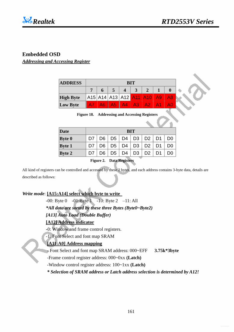
Realtek RTD2553V Series
161
Embedded OSD Addressing and Accessing Register
ADDRESS BIT 7 6 5 4 3 2 1 0 High Byte A15 A14 A13 A12 A11 A10 A9 A8 Low Byte A7 A6 A5 A4 A3 A2 A1 A0
Figure 18. Addressing and Accessing Registers
Date BIT Byte 0 D7 D6 D5 D4 D3 D2 D1 D0 Byte 1 D7 D6 D5 D4 D3 D2 D1 D0 Byte 2 D7 D6 D5 D4 D3 D2 D1 D0
Figure 2. Data Registers
All kind of registers can be controlled and accessed by these 2 bytes, and each address contains 3-byte data, details are
described as follows:
Write mode: [A15:A14] select which byte to write -00: Byte 0 -01:Byte 1 -10: Byte 2 –11: All
*All data are sorted by these three Bytes (Byte0~Byte2) [A13] Auto Load (Double Buffer)
[A12] Address indicator -0: Window and frame control registers. -1: Font Select and font map SRAM [A11:A0] Address mapping - Font Select and font map SRAM address: 000~EFF 3.75k*3byte -Frame control register address: 000~0xx (Latch) -Window control register address: 100~1xx (Latch) * Selection of SRAM address or Latch address selection is determined by A12!
http://www.DataSheet4U.net/
datasheet pdf - http://www.DataSheet4U.net/

Realtek RTD2553V Series
162
Example: Bit [15:14]=00
-All data followed are written to byte0 and address increases. Byte0àByte0àByte0… (Address will auto increase)
Bit [15:14] =01 -All data followed are written to byte1 and address increases.
Byte1àByte1àByte1… (Address will auto increase) Bit [15:14] =11
- Address will be increased after each 3-byte data written. Byte0àByte1àByte2àByte0àByte1àByte2… (Address will auto increase)
Window control registers
l Windows all support shadow/border/3D button l Window0, 5, 6, 7 support gradient functions. l Window 4, 5, 6, 7 start/end resolution are 1line(pixel), Window 0, 1, 2, 3 start/end resolution
are 4line(pixel), l All window start and end position include the special effect (border/shadow/3D button) been
assigned l Font comes after windows by 10 pixels, so you should compensate 10 pixels on windows to
meet font position Window 0 Shadow/Border/Gradient Address: 100h Byte 0
Bit Mode Function 7:6 -- Reserved 5:3 W Window 0 shadow/border width or 3D button thickness in pixel unit
000~111: 1 ~ 8 pixel 2:0 W Window 0 shadow/border height in line unit
000~111: 1 ~ 8 line It must be the same as bit[5:3] for 3D button thickness
Byte 1 Bit Mode Function 7:4 W Window 0 shadow color index in 16-color LUT
For 3D window, it is the left-top/bottom border color 3:0 W Window 0 border color index in 16-color LUT
http://www.DataSheet4U.net/
datasheet pdf - http://www.DataSheet4U.net/
Realtek RTD2553V Series
163
For 3D window, it is the right-bottom/top border color Byte 2
Bit Mode Function 7 W R Gradient Polarity
0: Decrease 1: Increase
6 W G Gradient Polarity 0: Decrease 1: Increase
5 W B Gradient Polarity 0: Decrease 1: Increase
4:3 W Gradient level 00: 1 step per level 01: Repeat 2 step per level 10: Repeat 3 step per level 11: Repeat 4 step per level
2 W Enable Red Color Gradient 1 W Enable Green Color Gradient 0 W Enable Blue Color Gradient
http://www.DataSheet4U.net/
datasheet pdf - http://www.DataSheet4U.net/
Realtek RTD2553V Series
164
Window 0 start position Address: 101h Byte 0
Bit Mode Function 7:2 W Window 0 horizontal start [5:0] 1:0 -- Reserved
Byte 1 Bit Mode Function 7:5 W Window 0 vertical start [2:0] line 4:0 W Window 0 horizontal start [10:6] pixel
Byte 2 Bit Mode Function 7:0 W Window 0 vertical start [10:3] line
Start position must be increments of four. Window 0 end position Address: 102h Byte 0
Bit Mode Function 7:2 W Window 0 horizontal end [5:0] 1:0 -- Reserved
Byte 1 Bit Mode Function 7:5 W Window 0 vertical end [2:0] line 4:0 W Window 0 horizontal end [10:6] pixel
Byte 2 Bit Mode Function 7:0 W Window 0 vertical end [10:3] line
l End position must be increments of four. Window 0 control Address: 103h Byte 0
Bit Mode Function 7:0 -- Reserved
Byte 1 Bit Mode Function 7 -- Reserved
http://www.DataSheet4U.net/
datasheet pdf - http://www.DataSheet4U.net/

Realtek RTD2553V Series
165
6:4 W 111: 7 level per gradient 110: 6 level per gradient 101: 5 level per gradient 100: 4 level per gradient 011: 3 level per gradient 010: 2 level per gradient 001: 1 level per gradient 000: 8 level per gradient
3:0 W Window 0 color index in 16-color LUT Byte 2 default: 00h
Bit Mode Function 7 W Reserved 6 W Gradient function
0: Disable 1: Enable
5 W Gradient direction 0: Horizontal 1: Vertical
4 W Shadow/Border/3D button 0: Disable 1: Enable
3:1 W Window 0 Type 000: Shadow Type 1 001: Shadow Type 2 010: Shadow Type3 011: Shadow Type 4 100: 3D Button Type 1 101: 3D Button Type 2 110: Reserved 111: Border
0 W Window 0 Enable 0: Disable 1: Enable
http://www.DataSheet4U.net/
datasheet pdf - http://www.DataSheet4U.net/

Realtek RTD2553V Series
166
Window 1 Shadow/Border/Gradient Address: 104h Byte 0
Bit Mode Function 7:6 W Reserved 5:3 W Window 1 shadow/border width or 3D button thickness in pixel unit
000~111: 1 ~ 8 pixel 2:0 W Window 1 shadow/border height in line unit
000~111: 1 ~ 8 line It must be the same as bit[5:3] for 3D button thickness
Byte 1 Bit Mode Function 7:4 W Window 1 shadow color index in 16-color LUT
For 3D window, it is the left-top/bottom border color 3:0 W Window 1 border color index in 16-color LUT
For 3D window, it is the right-bottom/top border color Byte 2
Bit Mode Function 7:0 W Reserved
Window 1 start position Address: 105h Byte 0
Bit Mode Function 7:2 W Window 1 horizontal start [5:0] 1:0 -- Reserved
Byte 1 Bit Mode Function 7:5 W Window 1 vertical start [2:0] line 4:0 W Window 1 horizontal start [10:6] pixel
Byte 2 Bit Mode Function 7:0 W Window 1 vertical start [10:3] line
Start position must be increments of four. Window 1 end position Address: 106h
http://www.DataSheet4U.net/
datasheet pdf - http://www.DataSheet4U.net/

Realtek RTD2553V Series
167
Byte 0 Bit Mode Function 7:2 W Window 1 horizontal end [5:0] 1:0 -- Reserved
Byte 1 Bit Mode Function 7:5 W Window 1 vertical end [2:0] line 4:0 W Window 1 horizontal end [10:6] pixel
Byte 2 Bit Mode Function 7:0 W Window 1 vertical end [10:3] line
End position must be increments of four.
http://www.DataSheet4U.net/
datasheet pdf - http://www.DataSheet4U.net/
Realtek RTD2553V Series
168
Window 1 control Address: 107h Byte 0
Bit Mode Function 7:0 -- Reserved
Byte 1 Bit Mode Function 7:4 -- Reserved 3:0 W Window 1 color index in 16-color LUT
Byte 2 default: 00h Bit Mode Function 7:5 W Reserved 4 W Shadow/Border/3D button
0: Disable 1: Enable
3:1 W Window 1 Type 000: Shadow Type 1 001: Shadow Type 2 010: Shadow Type3 011: Shadow Type 4 100: 3D Button Type 1 101: 3D Button Type 2 110: Reserved 111: Border
0 W Window 1 Enable 0: Disable 1: Enable
Window 2 Shadow/Border/Gradient Address: 108h Byte 0
Bit Mode Function 7:6 W Reserved 5:3 W Window 2 shadow/border width or 3D button thickness in pixel unit
000~111: 1 ~ 8 pixel 2:0 W Window 2 shadow/border height in line unit
000~111: 1 ~ 8 line It must be the same as bit[5:3] for 3D button thickness
http://www.DataSheet4U.net/
datasheet pdf - http://www.DataSheet4U.net/
Realtek RTD2553V Series
169
Byte 1
Bit Mode Function 7:4 W Window 2 shadow color index in 16-color LUT
For 3D window, it is the left-top/bottom border color 3:0 W Window 2 border color index in 16-color LUT
For 3D window, it is the right-bottom/top border color Byte 2
Bit Mode Function 7:0 W Reserved
Window 2 start position Address: 109h Byte 0
Bit Mode Function 7:2 W Window 2 horizontal start [5:0] 1:0 -- Reserved
Byte 1 Bit Mode Function 7:5 W Window 2 vertical start [2:0] line 4:0 W Window 2 horizontal start [10:6] pixel
Byte 2 Bit Mode Function 7:0 W Window 2 vertical start [10:3] line
Start position must be increments of four. Window 2 end position Address: 10Ah Byte 0
Bit Mode Function 7:2 W Window 2 horizontal end [5:0] 1:0 -- Reserved
Byte 1 Bit Mode Function 7:5 W Window 2 vertical end [2:0] line 4:0 W Window 2 horizontal end [10:6] pixel
Byte 2 Bit Mode Function
http://www.DataSheet4U.net/
datasheet pdf - http://www.DataSheet4U.net/

Realtek RTD2553V Series
170
7:0 W Window 2 vertical end [10:3] line End position must be increments of four. Window 2 control Address: 10Bh Byte 0
Bit Mode Function 7:0 -- Reserved
Byte 1 Bit Mode Function 7:4 -- Reserved 3:0 W Window 2 color index in 16-color LUT
Byte 2 default: 00h Bit Mode Function 7:5 W Reserved 4 W Shadow/Border/3D button
0: Disable 1: Enable
3:1 W Window 2 Type 000: Shadow Type 1 001: Shadow Type 2 010: Shadow Type3 011: Shadow Type 4 100: 3D Button Type 1 101: 3D Button Type 2 110: Reserved 111: Border
0 W Window 2 Enable 0: Disable 1: Enable
Window 3 Shadow/Border/Gradient Address: 10Ch Byte 0
Bit Mode Function 7:6 W Reserved 5:3 W Window 3 shadow/border width or 3D button thickness in pixel unit
000~111: 1 ~ 8 pixel 2:0 W Window 3 shadow/border height in line unit
http://www.DataSheet4U.net/
datasheet pdf - http://www.DataSheet4U.net/

Realtek RTD2553V Series
171
000~111: 1 ~ 8 line It must be the same as bit[5:3] for 3D button thickness
Byte 1 Bit Mode Function 7:4 W Window 3 shadow color index in 16-color LUT
For 3D window, it is the left-top/bottom border color 3:0 W Window 3 border color index in 16-color LUT
For 3D window, it is the right-bottom/top border color Byte 2
Bit Mode Function 7:0 W Reserved
Window 3 start position Address: 10Dh Byte 0
Bit Mode Function 7:2 W Window 3 horizontal start [5:0] 1:0 -- Reserved
Byte 1 Bit Mode Function 7:5 W Window 3 vertical start [2:0] line 4:0 W Window 3 horizontal start [10:6] pixel
Byte 2 Bit Mode Function 7:0 W Window 3 vertical start [10:3] line
Start position must be increments of four. Window 3 end position Address: 10Eh Byte 0
Bit Mode Function 7:2 W Window 3 horizontal end [5:0] 1:0 -- Reserved
Byte 1 Bit Mode Function 7:5 W Window 3 vertical end [2:0] line 4:0 W Window 3 horizontal end [10:6] pixel
http://www.DataSheet4U.net/
datasheet pdf - http://www.DataSheet4U.net/
Realtek RTD2553V Series
172
Byte 2 Bit Mode Function 7:0 W Window 3 vertical end [10:3] line
End position must be increments of four. Window 3 control Address: 10Fh Byte 0
Bit Mode Function 7:0 -- Reserved
Byte 1 Bit Mode Function 7:4 -- Reserved 3:0 W Window 3 color index in 16-color LUT
Byte 2 default: 00h Bit Mode Function 7:5 W Reserved 4 W Shadow/Border/3D button
0: Disable 1: Enable
3:1 W Window 3 Type 000: Shadow Type 1 001: Shadow Type 2 010: Shadow Type3 011: Shadow Type 4 100: 3D Button Type 1 101: 3D Button Type 2 110: Reserved 111: Border
0 W Window 3 Enable 0: Disable 1: Enable
Window 4 Shadow/Border/Gradient Address: 110h Byte 0
Bit Mode Function 7:6 W Reserved 5:3 W Window 4 shadow/border width or 3D button thickness in pixel unit
http://www.DataSheet4U.net/
datasheet pdf - http://www.DataSheet4U.net/

Realtek RTD2553V Series
173
000~111: 1 ~ 8 pixel 2:0 W Window 4 shadow/border height in line unit
000~111: 1 ~ 8 line It must be the same as bit[5:3] for 3D button thickness
Byte 1 Bit Mode Function 7:4 W Window 4 shadow color index in 16-color LUT
For 3D window, it is the left-top/ bottom border color 3:0 W Window 4 border color index in 16-color LUT
For 3D window, it is the right-bottom/top border color Byte 2
Bit Mode Function 7:0 W Reserved
Window 4 start position Address: 111h Byte 0
Bit Mode Function 7:2 W Window 4 horizontal start [5:0] 2:0 -- Reserved
Byte 1 Bit Mode Function 7:5 W Window 4 vertical start [2:0] line 4:0 W Window 4 horizontal start [10:6] pixel
Byte 2 Bit Mode Function 7:0 W Window 4 vertical start [10:3] line
Window 4 end position Address: 112h Byte 0
Bit Mode Function 7:2 W Window 4 horizontal end [5:0] 1:0 -- Reserved
Byte 1 Bit Mode Function 7:5 W Window 4 vertical end [2:0] line 4:0 W Window 4 horizontal end [10:6] pixel
http://www.DataSheet4U.net/
datasheet pdf - http://www.DataSheet4U.net/

Realtek RTD2553V Series
174
Byte 2 Bit Mode Function 7:0 W Window 4 vertical end [10:3] line
Window 4 control Address: 113h Byte 0
Bit Mode Function 7:0 -- Reserved
Byte 1 Bit Mode Function 7:4 -- Reserved 3:0 W Window 4 color index in 16-color LUT
Byte 2 default: 00h Bit Mode Function 7:5 W Reserved 4 W Shadow/Border/3D button
0: Disable 1: Enable
3:1 W Window 4 Type 000: Shadow Type 1 001: Shadow Type 2 010: Shadow Type3 011: Shadow Type 4 100: 3D Button Type 1 101: 3D Button Type 2 110: Reserved 111: Border
0 W Window 4 Enable 0: Disable 1: Enable
Window 5 Shadow/Border/Gradient Address: 114h Byte 0
Bit Mode Function 7:6 W Reserved 5:3 W Window 5 shadow/border width or 3D button thickness in pixel unit
000~111: 1 ~ 8 pixel
http://www.DataSheet4U.net/
datasheet pdf - http://www.DataSheet4U.net/

Realtek RTD2553V Series
175
2:0 W Window 5 shadow/border height in line unit 000~111: 1 ~ 8 line It must be the same as bit[5:3] for 3D button thickness
Byte 1 Bit Mode Function 7:4 W Window 5 shadow color index in 16-color LUT
For 3D window, it is the left-top/bottom border color 3:0 W Window 5 border color index in 16-color LUT
For 3D window, it is the right-bottom/top border color Byte 2
Bit Mode Function 7 W R Gradient Polarity
0: Decrease 1: Increase
6 W G Gradient Polarity 0: Decrease 1: Increase
5 W B Gradient Polarity 0: Decrease 1: Increase
4:3 W Gradient level 00: 1 step per level 01: Repeat 2 step per level 10: Repeat 3 step per level 11: Repeat 4 step per level
2 W Enable Red Color Gradient 1 W Enable Green Color Gradient 0 W Enable Blue Color Gradient
Window 5 start position Address: 115h Byte 0
Bit Mode Function 7:2 W Window 5 horizontal start [5:0] 1:0 -- Reserved
Byte 1 Bit Mode Function
http://www.DataSheet4U.net/
datasheet pdf - http://www.DataSheet4U.net/

Realtek RTD2553V Series
176
7:5 W Window 5 vertical start [2:0] line 4:0 W Window 5 horizontal start [10:6] pixel
Byte 2 Bit Mode Function 7:0 W Window 5 vertical start [10:3] line
Window 5 end position Address: 116h Byte 0
Bit Mode Function 7:2 W Window 5 horizontal end [5:0] 1:0 -- Reserved
Byte 1 Bit Mode Function 7:5 W Window 5 vertical end [2:0] line 4:0 W Window 5 horizontal end [10:6] pixel
Byte 2 Bit Mode Function 7:0 W Window 5 vertical end [10:3] line
Window 5 control Address: 117h Byte 0
Bit Mode Function 7:0 -- Reserved
Byte 1 Bit Mode Function 7 -- Reserved
6:4 W 111: 7 level per gradient 110: 6 level per gradient 101: 5 level per gradient 100: 4 level per gradient 011: 3 level per gradient 010: 2 level per gradient 001: 1 level per gradient 000: 8 level per gradient
3:0 W Window 5 color index in 16-color LUT
http://www.DataSheet4U.net/
datasheet pdf - http://www.DataSheet4U.net/
Realtek RTD2553V Series
177
Byte 2 default: 00h Bit Mode Function 7 W Reserved 6 W Gradient function
0: Disable 1: Enable
5 W Gradient direction 0: Horizontal 1: Vertical
4 W Shadow/Border/3D button 0: Disable 1: Enable
3:1 W Window 5 Type 000: Shadow Type 1 001: Shadow Type 2 010: Shadow Type3 011: Shadow Type 4 100: 3D Button Type 1 101: 3D Button Type 2 110: Reserved 111: Border
0 W Window 5 Enable 0: Disable 1: Enable
Window 6 Shadow/Border/Gradient Address: 118h Byte 0
Bit Mode Function 7:6 W Reserved 5:3 W Window 6 shadow/border width or 3D button thickness in pixel unit
000~111: 1 ~ 8 pixel 2:0 W Window 6 shadow/border height in line unit
000~111: 1 ~ 8 line It must be the same as bit[5:3] for 3D button thickness
PS: This is for non-rotary, rotate 270, rotate 90 and 180. Byte 1
Bit Mode Function
http://www.DataSheet4U.net/
datasheet pdf - http://www.DataSheet4U.net/

Realtek RTD2553V Series
178
7:4 W Window 6 shadow color index in 16-color LUT For 3D window, it is the left-top/ bottom border color
3:0 W Window 6 border color index in 16-color LUT For 3D window, it is the right-bottom/top border color
Byte 2 Bit Mode Function 7 W R Gradient Polarity
0: Decrease 1: Increase
6 W G Gradient Polarity 0: Decrease 1: Increase
5 W B Gradient Polarity 0: Decrease 1: Increase
4:3 W Gradient level 00: 1 step per level 01: Repeat 2 step per level 10: Repeat 3 step per level 11: Repeat 4 step per level
2 W Enable Red Color Gradient 1 W Enable Green Color Gradient 0 W Enable Blue Color Gradient
Window 6 start position Address: 119h Byte 0
Bit Mode Function 7:2 W Window 6 horizontal start [5:0] 1:0 -- Reserved
Byte 1 Bit Mode Function 7:5 W Window 6 vertical start [2:0] line 4:0 W Window 6 horizontal start [10:6] pixel
Byte 2 Bit Mode Function 7:0 W Window 6 vertical start [10:3] line
http://www.DataSheet4U.net/
datasheet pdf - http://www.DataSheet4U.net/
Realtek RTD2553V Series
179
Window 6 end position Address: 11Ah Byte 0
Bit Mode Function 7:2 W Window 6 horizontal end [5:0] 1:0 -- Reserved
Byte 1 Bit Mode Function 7:5 W Window 6 vertical end [2:0] line 4:0 W Window 6 horizontal end [10:6] pixel
Byte 2 Bit Mode Function 7:0 W Window 6 vertical end [10:3] line
Window 6 control Address: 11Bh Byte 0
Bit Mode Function 7:0 -- Reserved
Byte 1 Bit Mode Function 7 -- Reserved
6:4 W 111: 7 level per gradient 110: 6 level per gradient 101: 5 level per gradient 100: 4 level per gradient 011: 3 level per gradient 010: 2 level per gradient 001: 1 level per gradient 000: 8 level per gradient
3:0 W Window 6 color index in 16-color LUT Byte 2 default: 00h
Bit Mode Function 7 W Reserved 6 W Gradient function
0: Disable 1: Enable
http://www.DataSheet4U.net/
datasheet pdf - http://www.DataSheet4U.net/

Realtek RTD2553V Series
180
5 W Gradient direction 0: Horizontal 1: Vertical
4 W Shadow/Border/3D button 0: Disable 1: Enable
3:1 W Window 6 Type 000: Shadow Type 1 001: Shadow Type 2 010: Shadow Type3 011: Shadow Type 4 100: 3D Button Type 1 101: 3D Button Type 2 110: Reserved 111: Border
0 W Window 6 Enable 0: Disable 1: Enable
Window 7 Shadow/Border/Gradient Address: 11Ch Byte 0
Bit Mode Function 7:6 W Reserved 5:3 W Window 7 shadow/border width or 3D button thickness in pixel unit
000~111: 1 ~ 8 pixel 2:0 W Window 7 shadow/border height in line unit
000~111: 1 ~ 8 line It must be the same as bit[5:3] for 3D button thickness
PS: This is for non-rotary, rotate 270, rotate 90 and 180. Byte 1
Bit Mode Function 7:4 W Window 7 shadow color index in 16-color LUT
For 3D window, it is the left-top/bottom border color 3:0 W Window 7 border color index in 16-color LUT
For 3D window, it is the right-bottom/top border color Byte 2
Bit Mode Function
http://www.DataSheet4U.net/
datasheet pdf - http://www.DataSheet4U.net/

Realtek RTD2553V Series
181
7 W R Gradient Polarity 0: Decrease 1: Increase
6 W G Gradient Polarity 0: Decrease 1: Increase
5 W B Gradient Polarity 0: Decrease 1: Increase
4:3 W Gradient level 00: 1 step per level 01: Repeat 2 step per level 10: Repeat 3 step per level 11: Repeat 4 step per level
2 W Enable Red Color Gradient 1 W Enable Green Color Gradient 0 W Enable Blue Color Gradient
Window 7 start position Address: 11Dh Byte 0
Bit Mode Function 7:2 W Window 7 horizontal start [5:0] 1:0 -- Reserved
Byte 1 Bit Mode Function 7:5 W Window 7 vertical start [2:0] line 4:0 W Window 7 horizontal start [10:6] pixel
Byte 2 Bit Mode Function 7:0 W Window 7 vertical start [10:3] line
Window 7 end position Address: 11Eh Byte 0
Bit Mode Function 7:2 W Window 7 horizontal end [5:0] 1:0 -- Reserved
Byte 1
http://www.DataSheet4U.net/
datasheet pdf - http://www.DataSheet4U.net/

Realtek RTD2553V Series
182
Bit Mode Function 7:5 W Window 7 vertical end [2:0] line 4:0 W Window 7 horizontal end [10:6] pixel
Byte 2 Bit Mode Function 7:0 W Window 7 vertical end [10:3] line
Window 7 control Address: 11Fh Byte 0
Bit Mode Function 7:0 -- Reserved
Byte 1 Bit Mode Function 7 -- Reserved
6:4 W 111: 7 level per gradient 110: 6 level per gradient 101: 5 level per gradient 100: 4 level per gradient 011: 3 level per gradient 010: 2 level per gradient 001: 1 level per gradient 000: 8 level per gradient
3:0 W Window 7 color index in 16-color LUT Byte 2 default: 00h
Bit Mode Function 7 W Reserved 6 W Gradient function
0: Disable 1: Enable
5 W Gradient direction 0: Horizontal 1: Vertical
4 W Shadow/Border/3D button 0: Disable 1: Enable
3:1 W Window 7 Type
http://www.DataSheet4U.net/
datasheet pdf - http://www.DataSheet4U.net/

Realtek RTD2553V Series
183
000: Shadow Type 1 001: Shadow Type 2 010: Shadow Type3 011: Shadow Type 4 100: 3D Button Type 1 101: 3D Button Type 2 110: Reserved 111: Border
0 W Window 7 Enable 0: Disable 1: Enable
http://www.DataSheet4U.net/
datasheet pdf - http://www.DataSheet4U.net/
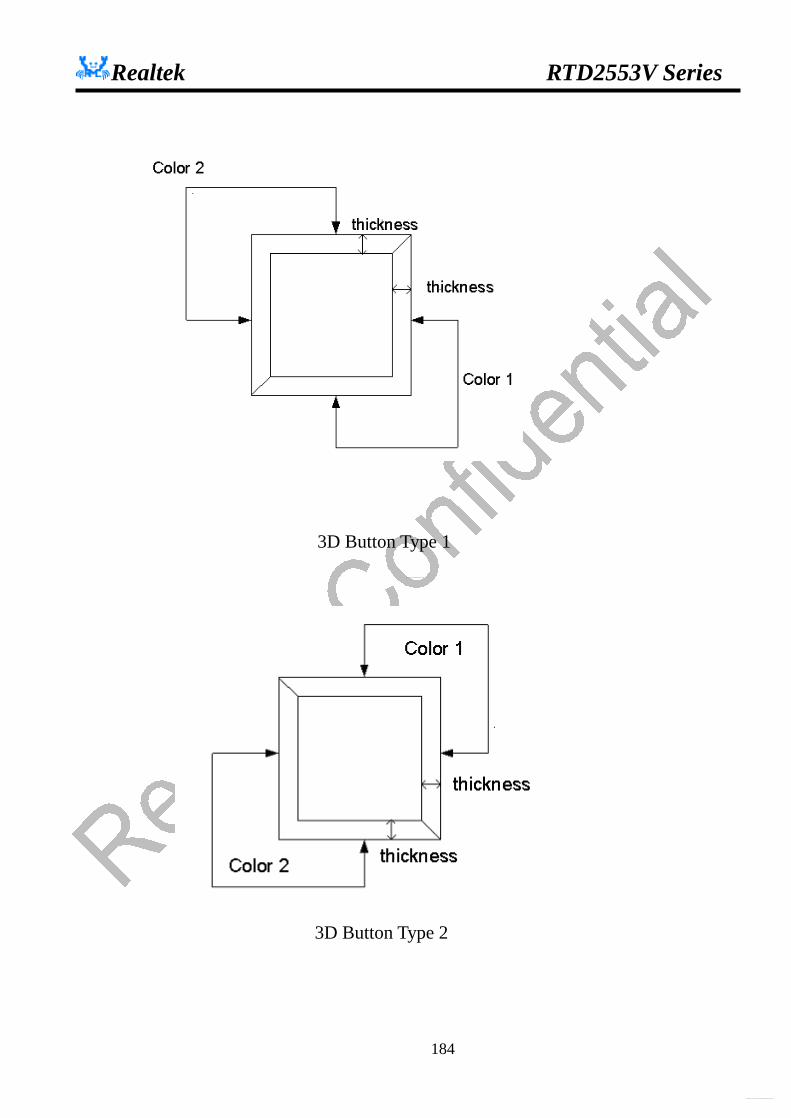
Realtek RTD2553V Series
184
3D Button Type 1
3D Button Type 2
http://www.DataSheet4U.net/
datasheet pdf - http://www.DataSheet4U.net/

Realtek RTD2553V Series
185
Type 1 Type 2 Type 3 Type 4
width
height
Shadow in all direction
OSD appear range transparent
start
end
Window mask fade/in out function
http://www.DataSheet4U.net/
datasheet pdf - http://www.DataSheet4U.net/
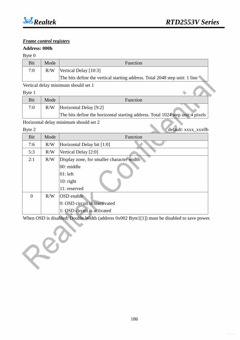
Realtek RTD2553V Series
186
Frame control registers Address: 000h Byte 0
Bit Mode Function 7:0 R/W Vertical Delay [10:3]
The bits define the vertical starting address. Total 2048 step unit: 1 line Vertical delay minimum should set 1 Byte 1
Bit Mode Function 7:0 R/W Horizontal Delay [9:2]
The bits define the horizontal starting address. Total 1024 step unit:4 pixels Horizontal delay minimum should set 2 Byte 2 default: xxxx_xxx0b
Bit Mode Function 7:6 R/W Horizontal Delay bit [1:0] 5:3 R/W Vertical Delay [2:0] 2:1 R/W Display zone, for smaller character width
00: middle 01: left 10: right 11: reserved
0 R/W OSD enable 0: OSD circuit is inactivated 1: OSD circuit is activated
When OSD is disabled, Double Width (address 0x002 Byte1[1]) must be disabled to save power.
http://www.DataSheet4U.net/
datasheet pdf - http://www.DataSheet4U.net/

Realtek RTD2553V Series
187
PWM Duty Width Address: 001h Byte 0 Default: 00h
Bit Mode Function 7:0 R/W PWM_0
8bits decides the output duty width and waveform of PWM at PWM channel
Byte 1 Default: 00h Bit Mode Function 7:0 R/W PWM_1
8bits decides the output duty width and waveform of PWM at PWM channel
Byte 2 Default: 00h Bit Mode Function 7:0 R/W PWM_2
8bits decides the output duty width and waveform of PWM at PWM channel
Address: 002h Byte 0 Default: 00h
Bit Mode Function 7:0 R/W First stage clock divider N[7:0]
N=0-255, 1st F= F/2(N+1) Byte 1 Default: 00h
Bit Mode Function 7 R/W PWM0 First stage clock divider Enable
0: Disable 1: Enable
6 R/W PWM1 First stage clock divider Enable 0: Disable 1: Enable
5 R/W PWM2 First stage clock divider Enable 0: Disable 1: Enable
4 R/W Enable PWM Output 3:2 R/W Crystal Clock Divider
00: Crystal 01: Crystal/2
http://www.DataSheet4U.net/
datasheet pdf - http://www.DataSheet4U.net/
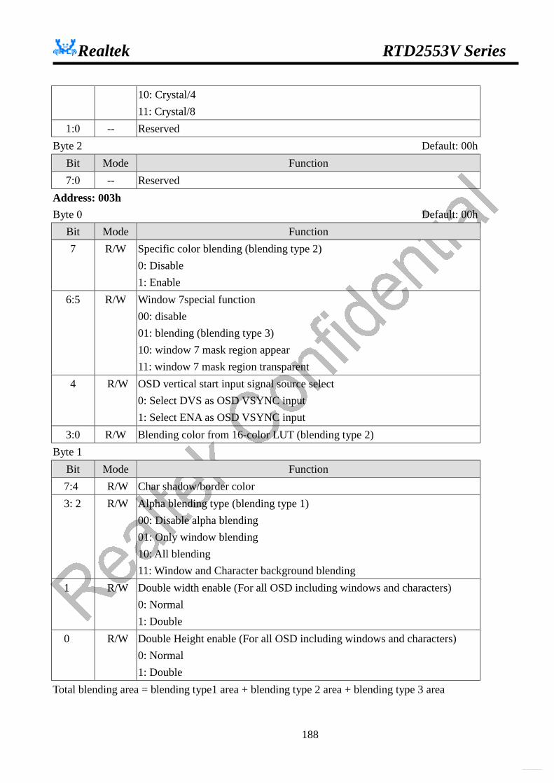
Realtek RTD2553V Series
188
10: Crystal/4 11: Crystal/8
1:0 -- Reserved Byte 2 Default: 00h
Bit Mode Function 7:0 -- Reserved
Address: 003h Byte 0 Default: 00h
Bit Mode Function 7 R/W Specific color blending (blending type 2)
0: Disable 1: Enable
6:5 R/W Window 7special function 00: disable 01: blending (blending type 3) 10: window 7 mask region appear 11: window 7 mask region transparent
4 R/W OSD vertical start input signal source select 0: Select DVS as OSD VSYNC input 1: Select ENA as OSD VSYNC input
3:0 R/W Blending color from 16-color LUT (blending type 2) Byte 1
Bit Mode Function 7:4 R/W Char shadow/border color 3: 2 R/W Alpha blending type (blending type 1)
00: Disable alpha blending 01: Only window blending 10: All blending 11: Window and Character background blending
1 R/W Double width enable (For all OSD including windows and characters) 0: Normal 1: Double
0 R/W Double Height enable (For all OSD including windows and characters) 0: Normal 1: Double
Total blending area = blending type1 area + blending type 2 area + blending type 3 area
http://www.DataSheet4U.net/
datasheet pdf - http://www.DataSheet4U.net/

Realtek RTD2553V Series
189
Byte 2 Bit Mode Function 7:6 R/W Font downloaded swap control
0x: No swap 10: CCW 11: CW
5:2 -- Reserved 1 R/W Global Blinking Enable
0: Disable 1: Enable
0 R/W Rotation 0: Normal (data latch 24 bit per 24 bit) 1: Rotation (data latch 18 bit per 24 bit)
Bit 7 6 5 4 3 2 1 0
Firmware A B C D E F G H CW A E B F C G D H
CCW E A F B G C H D
http://www.DataSheet4U.net/
datasheet pdf - http://www.DataSheet4U.net/
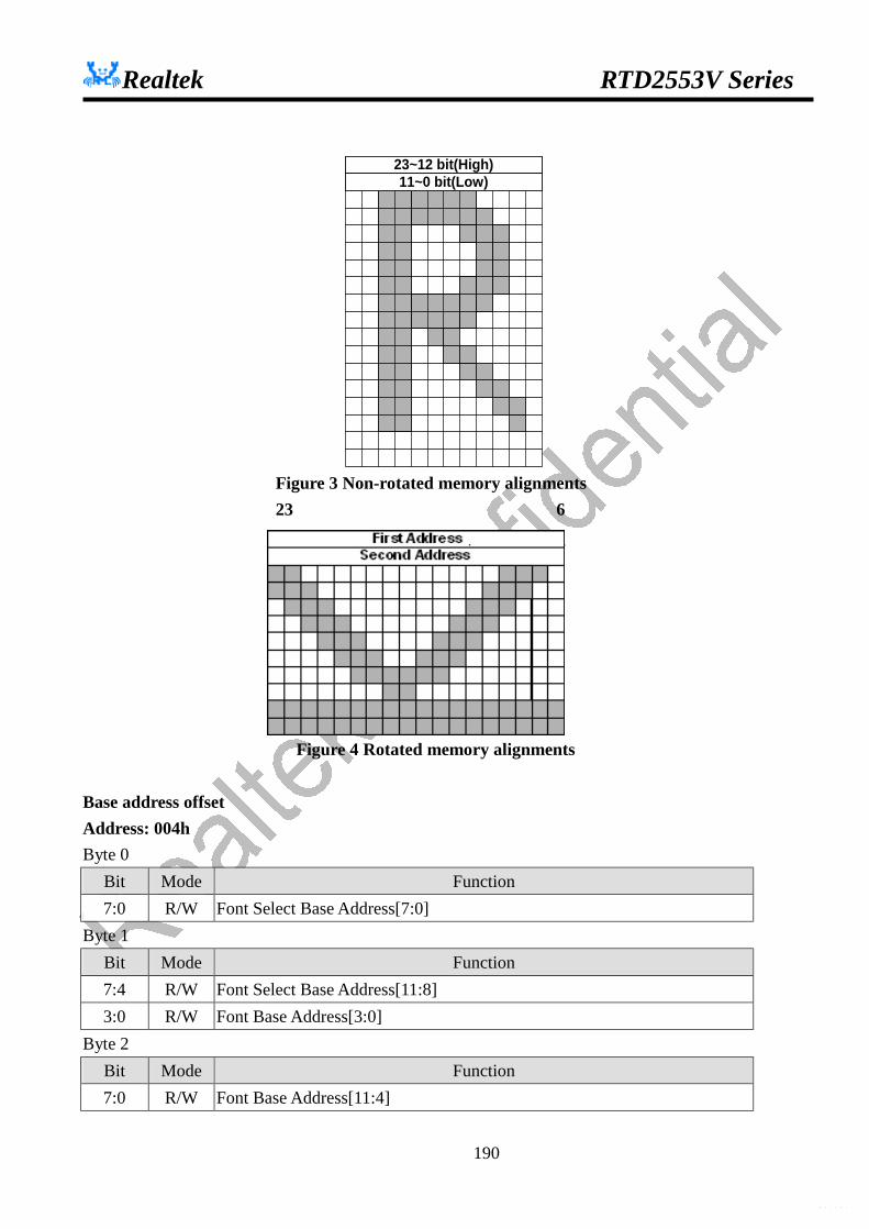
Realtek RTD2553V Series
190
Figure 3 Non-rotated memory alignments 23 6
Figure 4 Rotated memory alignments
Base address offset Address: 004h Byte 0
Bit Mode Function 7:0 R/W Font Select Base Address[7:0]
Byte 1 Bit Mode Function 7:4 R/W Font Select Base Address[11:8] 3:0 R/W Font Base Address[3:0]
Byte 2 Bit Mode Function 7:0 R/W Font Base Address[11:4]
23~12 bit(High)11~0 bit(Low)
h t t p : / / w w w . D a t a S h e e t 4 U . n e t /
d a t a s h e e t p d f - h t t p : / / w w w . D a t a S h e e t 4 U . n e t /

Realtek RTD2553V Series
191
OSD compression Address: 005h Byte 0
Bit Mode Function 7:4 R/W 4-bit value for VLC code 0 3:0 R/W 4-bit value for VLC code 100
Byte 1 Bit Mode Function 7:4 R/W 4-bit value for VLC code 1010 3:0 R/W 4-bit value for VLC code 1011
Byte 2 Bit Mode Function 7:4 R/W 4-bit value for VLC code 1100 3:0 R/W 4-bit value for VLC code 1101 0
Address: 006h Byte 0
Bit Mode Function 7:4 R/W 4-bit value for VLC code 1101 1 3:0 R/W 4-bit value for VLC code 1110 0
Byte 1 Bit Mode Function 7:4 R/W 4-bit value for VLC code 1110 10 3:0 R/W 4-bit value for VLC code 1110 11
Byte 2 Bit Mode Function 7:4 R/W 4-bit value for VLC code 1111 00 3:0 R/W 4-bit value for VLC code 1111 01
Address: 007h Byte 0
Bit Mode Function 7:4 R/W 4-bit value for VLC code 1111 100 3:0 R/W 4-bit value for VLC code 1111 101
Byte 1 Bit Mode Function
http://www.DataSheet4U.net/
datasheet pdf - http://www.DataSheet4U.net/

Realtek RTD2553V Series
192
7:4 R/W 4-bit value for VLC code 1111 110 3:0 R/W 4-bit value for VLC code 1111 1110
Byte 2 default: xxxx_xxx0b Bit Mode Function 7:1 -- reserved 0 R/W OSD compression (4bit/symbol, VLC code 1111_1111 represents the end of
data) (only for SRAM) 0: disable 1: enable
Note:
1. If enable OSD compression or auto load (double buffer), only one byte can be read after writing address at 0x90,
0x91.
2. For OSD compression, MSB 4 bits of original byte is first transferred to corresponding VLC code, and then LSB 4
bits is transf+erred. VLC code is placed from LSB to MSB of compression font. For example, 4-bit value for VLC
code 1100 is 4’b0101, and 4-bit value for VLC code 100 is 4’b0001. Original data 0x15 is transferred to
compression x0011001.
3. OSD double buffer and compression can’t be enabled simultaneous.
4. When power-down mode or lack of crystal clock, OSD compression font can’t be write.
5. After OSD enable, it is better to delay 1 DVS to start writing OSD compression data.
OSD SRAM (Map and font registers)
R0 R1 R2 …. Rn End C01 C02 B03 C04 … C11 C12 C13 …
… …
… Cn1 Cn2 … 1-bit font start … …
… 2-bit font start … …
4-bit font start … … …
11.25k bytes SRAM
1. Row Command
http://www.DataSheet4U.net/
datasheet pdf - http://www.DataSheet4U.net/
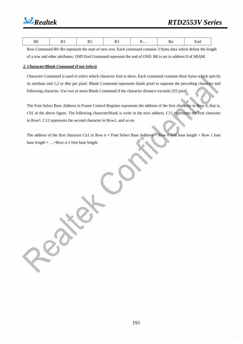
Realtek RTD2553V Series
193
R0 R1 R2 R3 R…. Rn End
Row Command R0~Rn represent the start of new row. Each command contains 3 bytes data which define the length
of a row and other attributes. OSD End Command represent the end of OSD. R0 is set in address 0 of SRAM.
2. Character/Blank Command (Font Select)
Character Command is used to select which character font is show. Each command contains three bytes which specify
its attribute and 1,2 or 4bit per pixel. Blank Command represents blank pixel to separate the preceding character and
following character. Use two or more Blank Command if the character distance exceeds 255 pixel.
The Font Select Base Address in Frame Control Register represents the address of the first character in Row 0, that is,
C01 in the above figure. The following character/blank is write in the next address. C11 represents the first character
in Row1, C12 represents the second character in Row1, and so on.
The address of the first character Cn1 in Row n = Font Select Base Address + Row 0 font base length + Row 1 font
base length + …+Row n-1 font base length.
http://www.DataSheet4U.net/
datasheet pdf - http://www.DataSheet4U.net/
Realtek RTD2553V Series
194
3. Font
User fonts are stored as bit map data. For normal font, one font has 12x18 pixel, and for rotation font, one has 18x12
pixel. One pixel use 1, 2 or 4 bits.
For 12x18 font,
One 1-bit font requires 9 * 24bit SRAM
One 2-bit font requires 18 * 24bit SRAM
One 4-bit font requires 36 * 24bit SRAM
For 18x12 font,
One 1-bit font requires 12 * 24bit SRAM
One 2-bit font requires 24 * 24bit SRAM
One 4-bit font requires 48 * 24bit SRAM
Font Base Address in Frame Control Register point to the start of 1-bit font.
For normal (12x18) font:
1-bit Font, if CS = 128, Real Address of Font = Font Base Address + 9 * 128
2-bit Font, if CS = 128, Real Address of Font = Font Base Address + 18 * 128
4-bit Font, if CS = 128, Real Address of Font = Font Base Address + 36 * 128
For rotational (18x12) font:
1-bit Font, if CS = 128, Real Address of Font = Font Base Address + 12 * 128
2-bit Font, if CS = 128, Real Address of Font = Font Base Address + 24 * 128
4-bit Font, if CS = 128, Real Address of Font = Font Base Address + 48 * 128
where CS is Character Selector in Character Command.
Note that Row Command, Font Select and Font share the same OSD SRAM.
When we download the font, we have to set the Frame control 002h byte1 [1:0] to set the method of hardware bit swap.
If the OSD is Counter-Clock-Wise rotated, we have to set to 0x01 (the 8 bits of every byte of font SRAM downloaded
by firmware will be in a sequence of “7 5 3 1 6 4 2 0” (from MSB to LSB) and should be rearranged to “7 6 5 4 3 2 1
0” by hardware). If it is Clock-Wise rotated, we have to set to 0x10 (the 8 bits of every byte of font SRAM downloaded
by firmware will be in a sequence of “6 4 2 0 7 5 3 1” (from MSB to LSB) and should be rearranged to “7 6 5 4 3 2 1
0” by hardware). After we finish the downloading or if we don’t have to rotate the OSD, we have to set it to 0x00.
http://www.DataSheet4U.net/
datasheet pdf - http://www.DataSheet4U.net/
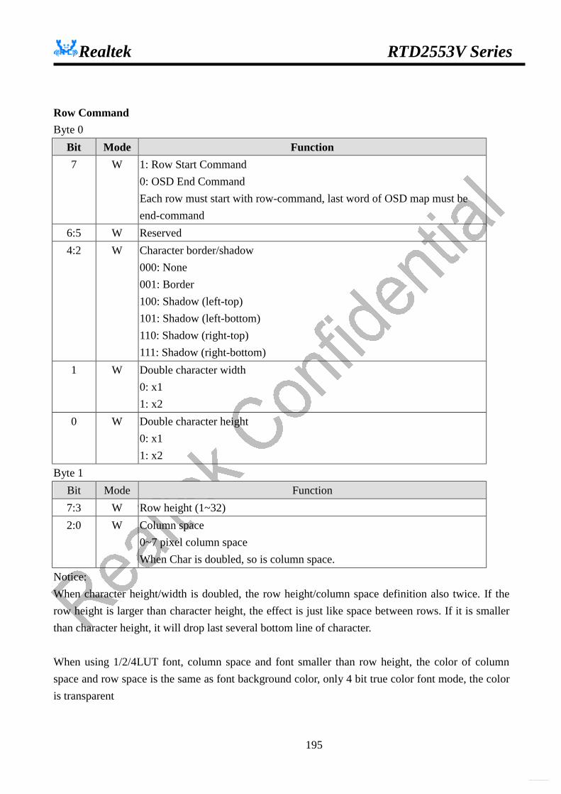
Realtek RTD2553V Series
195
Row Command Byte 0
Bit Mode Function 7 W 1: Row Start Command
0: OSD End Command Each row must start with row-command, last word of OSD map must be end-command
6:5 W Reserved 4:2 W Character border/shadow
000: None 001: Border 100: Shadow (left-top) 101: Shadow (left-bottom) 110: Shadow (right-top) 111: Shadow (right-bottom)
1 W Double character width 0: x1 1: x2
0 W Double character height 0: x1 1: x2
Byte 1 Bit Mode Function 7:3 W Row height (1~32) 2:0 W Column space
0~7 pixel column space When Char is doubled, so is column space.
Notice: When character height/width is doubled, the row height/column space definition also twice. If the row height is larger than character height, the effect is just like space between rows. If it is smaller than character height, it will drop last several bottom line of character. When using 1/2/4LUT font, column space and font smaller than row height, the color of column space and row space is the same as font background color, only 4 bit true color font mode, the color is transparent
http://www.DataSheet4U.net/
datasheet pdf - http://www.DataSheet4U.net/

Realtek RTD2553V Series
196
12
25 A1/2/4LUT bg color thesame as Characterbackground,4 true color mode, bgcolor is transparentRow space color
column space color
Byte 2
Bit Mode Function 7:0 W Row length unit: font base
Character Command (For blank) Byte 0
Bit Mode Function 7 W 0 6 W Blinking effect
0: Disable 1: Enable
5:0 W Reserved Byte 1
Bit Mode Function 7:0 W Blank pixel length
At least 3 pixels, and can’t exceed 255 pixels. Byte 2
Bit Mode Function 7:5 W Reserved 4 W Reserved
3:0 W Blank color – select one of 16-color LUT (0 is special for transparent)
http://www.DataSheet4U.net/
datasheet pdf - http://www.DataSheet4U.net/
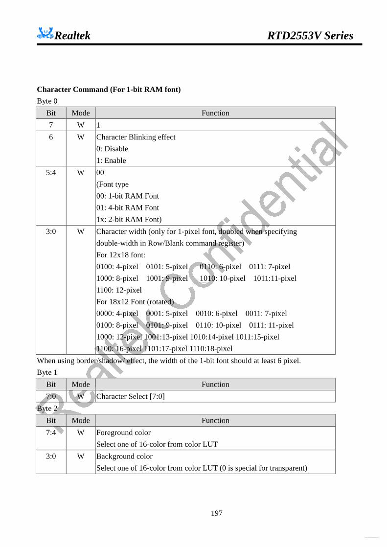
Realtek RTD2553V Series
197
Character Command (For 1-bit RAM font) Byte 0
Bit Mode Function 7 W 1 6 W Character Blinking effect
0: Disable 1: Enable
5:4 W 00 (Font type 00: 1-bit RAM Font 01: 4-bit RAM Font 1x: 2-bit RAM Font)
3:0 W Character width (only for 1-pixel font, doubled when specifying double-width in Row/Blank command register) For 12x18 font: 0100: 4-pixel 0101: 5-pixel 0110: 6-pixel 0111: 7-pixel 1000: 8-pixel 1001: 9-pixel 1010: 10-pixel 1011:11-pixel 1100: 12-pixel For 18x12 Font (rotated) 0000: 4-pixel 0001: 5-pixel 0010: 6-pixel 0011: 7-pixel 0100: 8-pixel 0101: 9-pixel 0110: 10-pixel 0111: 11-pixel 1000: 12-pixel 1001:13-pixel 1010:14-pixel 1011:15-pixel 1100: 16-pixel 1101:17-pixel 1110:18-pixel
When using border/shadow/ effect, the width of the 1-bit font should at least 6 pixel. Byte 1
Bit Mode Function 7:0 W Character Select [7:0]
Byte 2 Bit Mode Function 7:4 W Foreground color
Select one of 16-color from color LUT 3:0 W Background color
Select one of 16-color from color LUT (0 is special for transparent)
http://www.DataSheet4U.net/
datasheet pdf - http://www.DataSheet4U.net/

Realtek RTD2553V Series
198
Character command (For 2-bit RAM Font) Byte 0
Bit Mode Function 7 W 1 6 W MSB of Foreground color 11, Background 00 5 W 1 4 W MSB of Foreground color 10, Foreground 01
3:1 W Foreground color 11 Select one of 8 color from color LUT Add Byte0 [6] as MSB for 16-color LUT.
0 W Background color 00 Bit[2] Select one of 8 color from color LUT
Byte 1 Bit Mode Function 7:0 W Character Select [7:0]
Byte 2 Bit Mode Function 7:6 W Background color 00 Bit[1:0]
Select one of 8 color from color LUT While 0 is special for transparent Add Byte0 [6] as MSB for 16-color LUT. Once we fill 0000 or 1000(MSB follow Byte0[6]), BG appears transparent.
5:3 W Foreground color 10 Select one of 8 color from color LUT Add Byte0 [4] as MSB for 16-color LUT.
2:0 W Foreground color 01 Select one of 8 color from color LUT Add Byte0 [4] as MSB for 16-color LUT.
Character command (For 4-bit RAM font) Byte 0
Bit Mode Function 7 W 1 6 W Character Blinking effect
0: Disable 1: Enable
5:4 W 01
http://www.DataSheet4U.net/
datasheet pdf - http://www.DataSheet4U.net/

Realtek RTD2553V Series
199
(Font type 00: 1-bit RAM Font 01: 4-bit RAM Font 1x: 2-bit RAM Font)
3:0 W (for Byte1[7] = 0) select one color from 16-color LUT as background (for Byte1[7] = 1) Red color level MSB 4 bits for 8 bits color level (LSB 4 bits are 1111)
Byte 1 Bit Mode Function 7 W 0: 4bit Look Up Table, 0000’b is transparent.
1: 3bit specify R,G,B pattern, color level defined in Byte0[3:0],Byte2. One mask bit defines foreground or background.
6:0 W Character Select [6:0] l When 4-bit look-up table mode,color of column space is the same as background. l When 4-bit look-up table mode and pixel value is 0000, and byte0[3:0]=0000 means
transparent. l When true color mode and pixel value is 0000,it is transparent。 Byte 2
Bit Mode Function 7:4 W (for Byte1[7] = 1)
Green color level MSB 4 bits for 8 bits color level (LSB 4 bits are 1111)
3:0 W (for Byte1[7] = 1) Blue color level MSB 4 bits for 8 bits color level (LSB 4 bits are 1111)
http://www.DataSheet4U.net/
datasheet pdf - http://www.DataSheet4U.net/

Realtek RTD2553V Series
200
T
window 0
window 1window 2
window 3
window 4
window 5
A
window 7
window 6
Display Priority We have four windows with gradient and four windows without gradient, the window priority is as above, character should be always on the top layer of the window. Pattern gen. Use OSD to replace display pattern generator. Chess Board: make a font as below
If we want to fill to the full 1280x1024 screen with character, we need 1280*1024 pixels.
Required character is: Using 12*18 font 1280/12 = 106.7 -> 107 1024/18 = 56.9 -> 57 107*57 = 6099 character
http://www.DataSheet4U.net/
datasheet pdf - http://www.DataSheet4U.net/
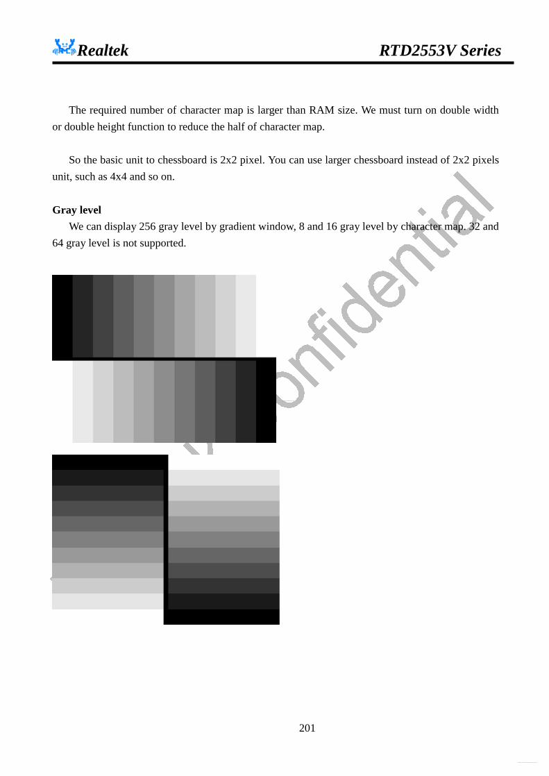
Realtek RTD2553V Series
201
The required number of character map is larger than RAM size. We must turn on double width
or double height function to reduce the half of character map. So the basic unit to chessboard is 2x2 pixel. You can use larger chessboard instead of 2x2 pixels
unit, such as 4x4 and so on.
Gray level We can display 256 gray level by gradient window, 8 and 16 gray level by character map. 32 and
64 gray level is not supported.
http://www.DataSheet4U.net/
datasheet pdf - http://www.DataSheet4U.net/

Realtek RTD2553V Series
202
http://www.DataSheet4U.net/
datasheet pdf - http://www.DataSheet4U.net/

Realtek RTD2553V Series
203
5.Electric Specification DC Characteristics Table 2 Absolute Maximum Ratings
PARAMETER SYMBOL MIN TYP MAX UNITS
Voltage on Input (5V tolerant) VIN -1 5 V
Electrostatic Discharge VESD ±2.5 kV
Latch-Up ILA ±100 mA
Ambient Operating Temperature TA 0 70 ºC
Storage temperature (plastic) TSTG -55 125 ºC
Thermal Resistance (Junction to Air) θJA 38 ºC/W
Table 3 DC Characteristics/Operating Condition (0℃<TA<70℃; VDD = 3.3V ± 0.3V)
PARAMETER SYMBOL MIN TYP MAX UNITS
Supply Voltage VDD 3.0 3.3 3.6 V
Supply Current(All function on at 135M)
● digital supply
● DCLK PLL supply
● MCLK PLL supply
IVDD
IDVCC
IAVCC
IPVCC
mA
Supply Current(Power Saving)
● digital supply
● DCLK PLL supply
● MCLK PLL supply
IVDD
IDVCC
IAVCC
IPVCC
mA
Output High Voltage VOH 2.4 VDD V
Output Low Voltage VOL GND 0.5 V
Input High Voltage VIH 2.0 V
Input Low Voltage VIL 0.8 V
I/O Pull-up resistance RPU 100 300 Ω
I/O Pull-down resistance RPD 50 150 Ω
Input Leakage Current(VI=VCC or GND) ILI -10 +10 μA
Output Leakage Current(VO=VCC or GND) ILO -20 +20 μA
http://www.DataSheet4U.net/
datasheet pdf - http://www.DataSheet4U.net/
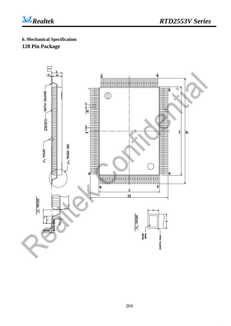
Realtek RTD2553V Series
204
6. Mechanical Specification 128 Pin Package
h t t p : / / w w w . D a t a S h e e t 4 U . n e t /
d a t a s h e e t p d f - h t t p : / / w w w . D a t a S h e e t 4 U . n e t /

Realtek RTD2553V Series
205
Note: Symbol Dimension in
inch
Dimension in
mm
1.Dimension D & E do not include interlead
Min Type Max Min Type Max flash.
A - 0.134 - - 3.40 2.Dimension b does not include dambar
A1 0.004 0.010 0.036 0.10 0.25 0.91 protrusion/intrusion.
A2 0.102 0.112 0.122 2.60 2.85 3.10 3.Controlling dimension: Millimeter
b 0.005 0.009 0.013 0.12 0.22 0.32 4.General appearance spec. should be based
c 0.002 0.006 0.010 0.05 0.15 0.25 on final visual inspection spec.
D 0.541 0.551 0.561 13.75 14.00 14.25 TITLE : 128LD QFP ( 14x20 mm*2 ) PACKAGE OUTLINE
E 0.778 0.787 0.797 19.75 20.00 20.25 -CU L/F, FOOTPRINT 3.2 mm
e 0.010 0.020 0.030 0.25 0.5 0.75 LEADFRAME MATERIAL:
HD 0.665 0.677 0.689 16.90 17.20 17.50 APPROVE DOC. NO. 530-ASS-P004
HE 0.902 0.913 0.925 22.90 23.20 23.50 VERSION 1
L 0.027 0.035 0.043 0.68 0.88 1.08 PAGE OF
L1 0.053 0.063 0.073 1.35 1.60 1.85 CHECK DWG NO. Q128 - 1
y - - 0.004 - - 0.10 DATE MAR. 25.1997
θ 0° - 12° 0° - 12° REALTEK SEMI-CONDUCTOR CO., LTD
http://www.DataSheet4U.net/
datasheet pdf - http://www.DataSheet4U.net/

Realtek RTD2553V Series
206
7. Ordering Information The available RTD2553V series pin compatible products listed below: Part Number ADC DVI HDCP Resolution Output Package
RTD2553V 210MHz ( 2 ports)
Yes No WUXGA/UXGA/WSXGA+
LVDS/RSDS/TTL 128 QFP
RTD2533V 165MHz (2 ports)
Yes No SXGA/WXGA+ LVDS/RSDS/TTL 128 QFP
RTD2033V 165MHz (2 ports)
No No SXGA/WXGA+ LVDS/RSDS/TTL 128 QFP
RTD2553VH 210MHz ( 2 ports)
Yes Yes WUXGA/UXGA/WSXGA+
LVDS/RSDS/TTL 128 QFP
RTD2533VH 165MHz (2 ports)
Yes Yes SXGA/WXGA+ LVDS/RSDS/TTL 128 QFP
RTD2553V-LF 210MHz ( 2 ports)
Yes No WUXGA/UXGA/WSXGA+
LVDS/RSDS/TTL 128 QFP
(lead free)
RTD2533V-LF 165MHz (2 ports)
Yes No SXGA/WXGA+ LVDS/RSDS/TTL 128 QFP
(lead free)
RTD2033V-LF 165MHz (2 ports)
No No SXGA/WXGA+ LVDS/RSDS/TTL 128 QFP
(lead free)
RTD2553VH-LF 210MHz ( 2 ports)
Yes Yes WUXGA/UXGA/WSXGA+
LVDS/RSDS/TTL 128 QFP
(lead free)
RTD2533VH-LF 165MHz (2 ports)
Yes Yes SXGA/WXGA+ LVDS/RSDS/TTL 128 QFP
(lead free)
* lead free packages are available for above items with suffix –LF.
http://www.DataSheet4U.net/
datasheet pdf - http://www.DataSheet4U.net/