Embed Size (px)
Citation preview

Redpine Signals, Inc.
RS-9110-N-11-24 Self Contained
802.11 b/g/n Module with Networking Stack
DDaattaasshheeeett
VVeerrssiioonn 22..22
NNoovveemmbbeerr 22001122
Redpine Signals, Inc. 2107 N. First Street, #680
San Jose, CA 95131.
Tel: (408) 748-3385
Fax: (408) 705-2019
Email: [email protected]
Website: www.redpinesignals.com

Redpine Signals, Inc. Page 2
RRSS--99111100--NN--1111--2244 SSeellff CCoonnttaaiinneedd 880022..1111 bb//gg//nn
MMoodduullee wwiitthh NNeettwwoorrkkiinngg SSttaacckk
DDaattaasshheeeett
VVeerrssiioonn 22..22
The RS9110-N-11-24 module is a IEEE
802.11bgn based WLAN device that
directly provides a wireless interface to
any equipment with a UART or SPI
interface for data transfer. It integrates a
MAC, baseband processor, RF transceiver
with power amplifier in hardware; and all
WLAN protocol and configuration
functionality, networking stack in
embedded firmware to make a fully self-
contained 802.11n WLAN solution for a
variety of applications.
Applications:
Seamless Wi-Fi connectivity for Application Processors
Industrial M2M communications
Point of Sale Terminals
Metering (Parking Meters, Utility Meters, Power Meters, etc.)
Security Cameras and Surveillance
Equipment
Logistics and Freight Management
Warehousing
Digital Picture Frames
Several medical applications
including Patient Monitoring,
Remote Diagnostics
Device Features:
802.11b/g and single stream
802.11n module
Supports WPA2-PSK, WEP (64 and
128 bit) and TKIP security in
infrastructure mode
Supports WEP (64 and 128 bit)
mode of security in ad-hoc mode
Host interface through UART and
SPI
Integrated TCP/IP stack with option
to bypass the stack in SPI mode
Ultra-low-power operation with
power-save modes
Ad-hoc and infrastructure modes for
maximum deployment flexibility
Configure module wirelessly for
easy field deployment, in SPI mode
Single supply – 3.1 to 3.6V
operation
Pad for external antenna connection
Device Dimensions 13.7 mm x 12.9 mm x 1.7mm
RS9110-N-11-24 System Block Diagram
RS9110-N-11-24
RF Transceiver+
PABalun
Flash
T/RSwitch
UART
SPI
3.3V
Reference Frequency
UART/SPI Select
Reset
RS9110
(TCP/UDP,
WLAN Stack)
Host Processor
Applications
Interrupt
Redpine Signals, Inc. Page 3
RRSS--99111100--NN--1111--2244 SSeellff CCoonnttaaiinneedd 880022..1111 bb//gg//nn
MMoodduullee wwiitthh NNeettwwoorrkkiinngg SSttaacckk
DDaattaasshheeeett
VVeerrssiioonn 22..22
Table of Contents
RS-9110-N-11-24 Self Contained 802.11 b/g/n Module with
Networking Stack ..................................................................... 1
1: Detailed Feature List ............................................................ 7 1.1: Host Interfaces ........................................................................ 7 1.2: WLAN ....................................................................................... 7
1.2.1: MAC .............................................................................................. 7 1.2.2: Baseband Processing .................................................................... 7 1.2.3: RF ................................................................................................. 7
1.3: Networking Protocols .............................................................. 7 1.4: Configuration ........................................................................... 8 1.5: Software .................................................................................. 8 1.6: Compliance and Certification ................................................... 8
2: Package Description ............................................................. 9 2.1: Top View .................................................................................. 9 2.2: Bottom View ............................................................................ 9 2.3: Package Dimensions .............................................................. 10 2.4: PCB Landing Pattern .............................................................. 11 2.5: Recommended Reflow Profile ................................................ 12 2.6: Baking Instructions ............................................................... 12
3: Pin Description ................................................................... 13 3.1: Module Pinout ........................................................................ 13 3.2: Pin Description ....................................................................... 13
4: Electrical Characteristics .................................................... 18 4.1: Absolute Maximum Ratings .................................................... 18 4.2: Recommended Operating Conditions ..................................... 18 4.3: DC Characteristics – Digital I/O Signals ................................. 18 4.4: AC Characteristics – Digital I/O Signals ................................. 19
4.4.1: SPI Interface .............................................................................. 19
5: Reset Sequence and Timing ................................................ 20
6: Performance Specifications ................................................ 21 6.1: Wireless Specifications .......................................................... 21 6.2: Receive Characteristics .......................................................... 21
6.2.1: Sensitivity................................................................................... 21 6.3: Throughput ............................................................................ 21 6.4: Range .................................................................................... 22 6.5: Standards Compliance ........................................................... 22
7: Software Architecture Overview ......................................... 23 7.1: Host ....................................................................................... 24
7.1.1: UART .......................................................................................... 24 7.1.2: SPI ............................................................................................. 24 7.1.3: Thin SPI Driver ........................................................................... 24
7.2: RS9110-N-11-24 .................................................................... 24 7.2.1: SPI ............................................................................................. 24
Redpine Signals, Inc. Page 4
RRSS--99111100--NN--1111--2244 SSeellff CCoonnttaaiinneedd 880022..1111 bb//gg//nn
MMoodduullee wwiitthh NNeettwwoorrkkiinngg SSttaacckk
DDaattaasshheeeett
VVeerrssiioonn 22..22
7.2.2: UART .......................................................................................... 24 7.2.3: Host Abstraction Layer (HAL) ..................................................... 25 7.2.4: Wireless Control Block (WCB) ..................................................... 25
7.2.4.1: TCP/IP Control frames .......................................................... 25 7.2.5: Station Management Entity (SME) .............................................. 25 7.2.6: WPA Supplicant .......................................................................... 25 7.2.7: Power Save Modes ...................................................................... 25
7.2.7.1: Power mode 0 ....................................................................... 25 7.2.7.2: Power mode 1 ....................................................................... 25 7.2.7.3: Power mode 2 ....................................................................... 26
8: Ordering Information ......................................................... 27
9: Command Reference (AT commands and SPI commands) .. 28

Redpine Signals, Inc. Page 5
RRSS--99111100--NN--1111--2244 SSeellff CCoonnttaaiinneedd 880022..1111 bb//gg//nn
MMoodduullee wwiitthh NNeettwwoorrkkiinngg SSttaacckk
DDaattaasshheeeett
VVeerrssiioonn 22..22
Table of Figures
Figure 1: Top View of the Module ................................................................. 9 Figure 2: Bottom View of the Module ........................................................... 9 Figure 3: Package Dimensions ................................................................... 10 Figure 4: PCB Landing Pattern.................................................................... 11 Figure 5: Reflow Profile .............................................................................. 12 Figure 6: Pinout of the Module ................................................................... 13 Figure 7: Interface Timings – SPI Interface ............................................... 19 Figure 8: Reset Pin Timing Diagram ........................................................... 20 Figure 9: RS9110-N-11-24 Software Architecture Block Diagram .............. 23

Redpine Signals, Inc. Page 6
RRSS--99111100--NN--1111--2244 SSeellff CCoonnttaaiinneedd 880022..1111 bb//gg//nn
MMoodduullee wwiitthh NNeettwwoorrkkiinngg SSttaacckk
DDaattaasshheeeett
VVeerrssiioonn 22..22
List of Tables
Table 1: Absolute Maximum Ratings .......................................................... 18 Table 2: Recommended Operating Conditions ............................................ 18 Table 3: Input/Output DC Characteristics .................................................. 19 Table 4: AC Characteristics – SPI Interface ................................................ 19 Table 5: Wireless Specificiation .................................................................. 21 Table 6: Receive sensitivity ........................................................................ 21 Table 7: Device Ordering Information ........................................................ 27
Redpine Signals, Inc. Page 7
RRSS--99111100--NN--1111--2244 SSeellff CCoonnttaaiinneedd 880022..1111 bb//gg//nn
MMoodduullee wwiitthh NNeettwwoorrkkiinngg SSttaacckk
DDaattaasshheeeett
VVeerrssiioonn 22..22
1: Detailed Feature List
1.1: Host Interfaces
UART
The UART interface supports standard baud rates from 9600 to
3686400 bps
AT Command Interface for configuration and operating the module
SPI Interface
Standard 4-wire SPI
Operation up to a maximum clock speed of 25 MHz
1.2: WLAN
1.2.1: MAC
Conforms to IEEE 802.11b/g/n standards for MAC
Dynamic selection of fragment threshold, data rate depending on the
channel statistics
Hardware accelerated implementation for AES
WPA2 and WEP support
Infrastructure and Ad-hoc modes
1.2.2: Baseband Processing
Supports DSSS (1, 2 Mbps) and CCK (5.5, 11 Mbps) modes
Supports all OFDM data rates (6, 9, 12, 18, 24, 36, 48, and 54 Mbps)
Supports IEEE 802.11n single-stream modes with data rates up to 65
Mbps
Supports long, short, and HT preamble modes
High-performance multipath compensation in OFDM, DSSS, and CCK
modes
1.2.3: RF
Highly integrated 2.4 GHz transceiver with direct conversion architecture
Receiver with 38 dB RF selectable gain range and 60 dB baseband variable
gain range
Power amplifier with 19 dBm output power for 11b and 17 dBm for 11g
and 11n
Integrated LNA, BPF, and T/R switch
1.3: Networking Protocols
TCP
UDP
Redpine Signals, Inc. Page 8
RRSS--99111100--NN--1111--2244 SSeellff CCoonnttaaiinneedd 880022..1111 bb//gg//nn
MMoodduullee wwiitthh NNeettwwoorrkkiinngg SSttaacckk
DDaattaasshheeeett
VVeerrssiioonn 22..22
ARP
ICMP
DHCP
The RS9110-N-11-24 comes with flexible frameworks to enable usage in
various application scenarios, viz., high throughput, more network features,
etc. Please contact Redpine for addition of network features like HTTP server.
1.4: Configuration
The RS9110-N-11-24 module can be configured through UART or SPI. The
following are some of the commands that can be given to the module:
Scan
Connect
Pre-shared Keys
SSID of hidden WLAN networks
DHCP Enable/Disable
Create/Join an IBSS network
Open/Close sockets for TCP, UDP, Listening TCP
1.5: Software
Sample Host driver for SPI
Configuration and management GUI for Windows XP for UART
Embedded software for complete WLAN functionality including 802.11n
aggregation and Block-ACK, auto rate adaptation, security and also
complete network stack and applications including TCP, UDP, ARP, ICMP.
DHCP.
The module, in SPI mode, can be made to come up as an Access point, to
which a standard WLAN device such as a laptop can connect and configure
the module or upgrade the firmware
1.6: Compliance and Certification
RS9110-N-11-24 is identical in hardware to RS9110-N-02 module which is
FCC, IC, and CE certified. RF Testing Software is provided for any end
product certification requirements.
RoHS (Restriction of Hazardous Substances) compliant

Redpine Signals, Inc. Page 9
RRSS--99111100--NN--1111--2244 SSeellff CCoonnttaaiinneedd 880022..1111 bb//gg//nn
MMoodduullee wwiitthh NNeettwwoorrkkiinngg SSttaacckk
DDaattaasshheeeett
VVeerrssiioonn 22..22
2: Package Description
2.1: Top View
Figure 1: Top View of the Module
2.2: Bottom View
Figure 2: Bottom View of the Module
Redpine Signals, Inc. Page 10
RRSS--99111100--NN--1111--2244 SSeellff CCoonnttaaiinneedd 880022..1111 bb//gg//nn
MMoodduullee wwiitthh NNeettwwoorrkkiinngg SSttaacckk
DDaattaasshheeeett
VVeerrssiioonn 22..22
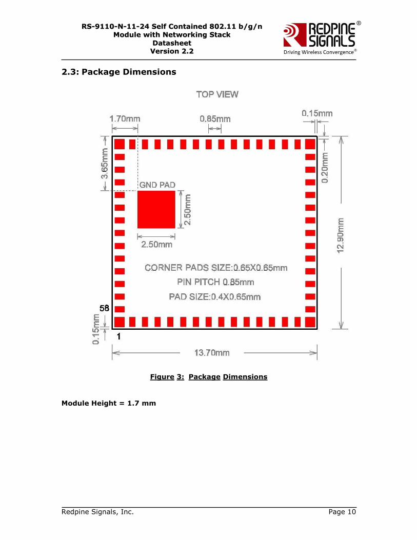
2.3: Package Dimensions
Figure 3: Package Dimensions
Module Height = 1.7 mm
Redpine Signals, Inc. Page 11
RRSS--99111100--NN--1111--2244 SSeellff CCoonnttaaiinneedd 880022..1111 bb//gg//nn
MMoodduullee wwiitthh NNeettwwoorrkkiinngg SSttaacckk
DDaattaasshheeeett
VVeerrssiioonn 22..22
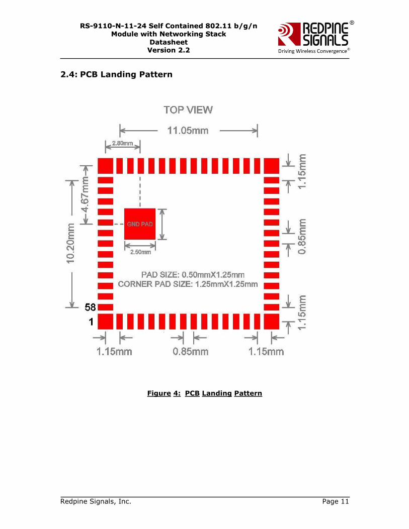
2.4: PCB Landing Pattern
Figure 4: PCB Landing Pattern
Redpine Signals, Inc. Page 12
RRSS--99111100--NN--1111--2244 SSeellff CCoonnttaaiinneedd 880022..1111 bb//gg//nn
MMoodduullee wwiitthh NNeettwwoorrkkiinngg SSttaacckk
DDaattaasshheeeett
VVeerrssiioonn 22..22
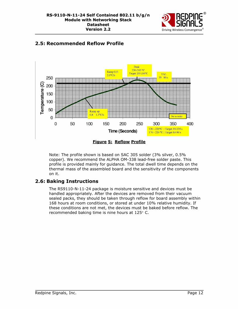
2.5: Recommended Reflow Profile
Figure 5: Reflow Profile
Note: The profile shown is based on SAC 305 solder (3% silver, 0.5%
copper). We recommend the ALPHA OM-338 lead-free solder paste. This
profile is provided mainly for guidance. The total dwell time depends on the
thermal mass of the assembled board and the sensitivity of the components
on it.
2.6: Baking Instructions
The RS9110-N-11-24 package is moisture sensitive and devices must be
handled appropriately. After the devices are removed from their vacuum
sealed packs, they should be taken through reflow for board assembly within
168 hours at room conditions, or stored at under 10% relative humidity. If
these conditions are not met, the devices must be baked before reflow. The
recommended baking time is nine hours at 125 C.
Redpine Signals, Inc. Page 13
RRSS--99111100--NN--1111--2244 SSeellff CCoonnttaaiinneedd 880022..1111 bb//gg//nn
MMoodduullee wwiitthh NNeettwwoorrkkiinngg SSttaacckk
DDaattaasshheeeett
VVeerrssiioonn 22..22
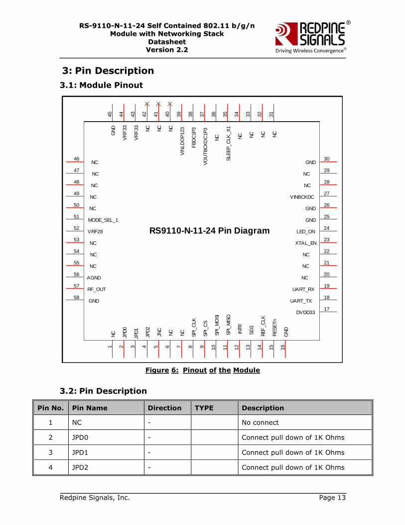
3: Pin Description
3.1: Module Pinout
AGND56
RF_OUT57
GND58
GND25
NC
1
DVDD3317
NC
40
LED_ON24
MODE_SEL_151
VRF2852
XTAL_EN23
REF
_C
LK
14
NC46 S
LE
EP
_C
LK
_X
135
NC
34
NC
6
NC
7
GND30
GND26
RE
SE
Tn
15
NC
41
NC
31
NC29
NC
32
NC53
NC
42
VR
F33
43
VR
F33
44
SD
313
INTR
12
SPI_
MIS
O11
SPI_
MO
SI
10
SPI_
CS
9
SPI_
CLK
8
NC55
GN
D16
VINBCKDC27
VIN
LD
OP
123
39
FB
DC
1P
338
VO
UT
BC
KD
C1P
337
NC
36
NC22
NC21
UART_TX18
UART_RX19
JPD
02
JPD
13
JPD
24
JNC
5
NC54
NC28
NC
33
NC20
NC47
GN
D45
NC50
NC49
NC48
RS9110-N-11-24 Pin Diagram
Figure 6: Pinout of the Module
3.2: Pin Description
Pin No. Pin Name Direction TYPE Description
1 NC - No connect
2 JPD0 - Connect pull down of 1K Ohms
3 JPD1 - Connect pull down of 1K Ohms
4 JPD2 - Connect pull down of 1K Ohms

Redpine Signals, Inc. Page 14
RRSS--99111100--NN--1111--2244 SSeellff CCoonnttaaiinneedd 880022..1111 bb//gg//nn
MMoodduullee wwiitthh NNeettwwoorrkkiinngg SSttaacckk
DDaattaasshheeeett
VVeerrssiioonn 22..22
Pin No. Pin Name Direction TYPE Description
5 JNC - No connect
6 NC - No connect
7 NC - No connect
8 SPI_CLK Input LVCMOS
SPI Clock input. SPI Data Input.
In UART mode, connect pull-down (1K to 10K Ohms)
9 SPI_CS Input LVCMOS
8mA
Active low SPI Chip Select. SPI Data
Input.
In UART mode, connect pull-down (1K to 10K Ohms)
10 SPI_MOSI Input LVCMOS
8mA
SPI Data Input.
In UART mode, connect pull-down (1K to 10K Ohms)
11 SPI_MISO Output LVCMOS
8mA
SPI Data output. No connect in UART
mode.
12 INTR Output LVCMOS
8mA
Interrupt to the host. Active high,
level triggered. Asserted by the module when:
1.The module has to transmit data to
the host through SPI
2.When the module wakes up from sleep mode
13 SD3 -
No connect in SPI mode. In UART
mode, connect pull-down (1K to 10K Ohms)
14 REF_CLK Input Reference Clock source: 40 MHz.
15 RESET_n Input LVCMOS
Power-on reset. Active low, and
required to be active for at least 10 ms
16 GND Ground
Ground. Ground. Connect all the GND
pins directly to a ground plane or
copper ground fill
17 DVDD33 Power 3.3 Volts Input to the I/O Rail
18 UART_TX Output LVCMOS
4mA
UART output. No connect in SPI
mode.
19 UART_RX Input LVCMOS
4mA UART input. No connect in SPI mode.
20 NC - No connect
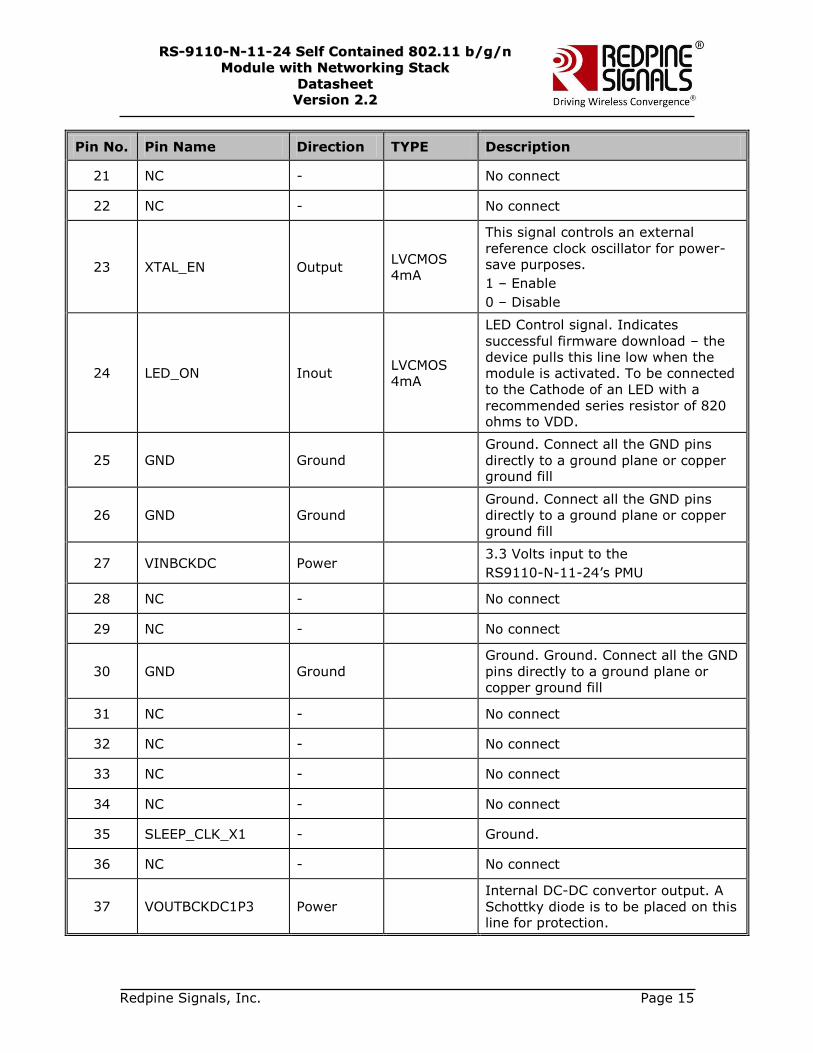
Redpine Signals, Inc. Page 15
RRSS--99111100--NN--1111--2244 SSeellff CCoonnttaaiinneedd 880022..1111 bb//gg//nn
MMoodduullee wwiitthh NNeettwwoorrkkiinngg SSttaacckk
DDaattaasshheeeett
VVeerrssiioonn 22..22
Pin No. Pin Name Direction TYPE Description
21 NC - No connect
22 NC - No connect
23 XTAL_EN Output LVCMOS
4mA
This signal controls an external
reference clock oscillator for power-save purposes.
1 – Enable
0 – Disable
24 LED_ON Inout LVCMOS
4mA
LED Control signal. Indicates
successful firmware download – the
device pulls this line low when the
module is activated. To be connected
to the Cathode of an LED with a
recommended series resistor of 820 ohms to VDD.
25 GND Ground
Ground. Connect all the GND pins
directly to a ground plane or copper ground fill
26 GND Ground
Ground. Connect all the GND pins
directly to a ground plane or copper
ground fill
27 VINBCKDC Power 3.3 Volts input to the
RS9110-N-11-24’s PMU
28 NC - No connect
29 NC - No connect
30 GND Ground
Ground. Ground. Connect all the GND
pins directly to a ground plane or
copper ground fill
31 NC - No connect
32 NC - No connect
33 NC - No connect
34 NC - No connect
35 SLEEP_CLK_X1 - Ground.
36 NC - No connect
37 VOUTBCKDC1P3 Power
Internal DC-DC convertor output. A
Schottky diode is to be placed on this line for protection.
Redpine Signals, Inc. Page 16
RRSS--99111100--NN--1111--2244 SSeellff CCoonnttaaiinneedd 880022..1111 bb//gg//nn
MMoodduullee wwiitthh NNeettwwoorrkkiinngg SSttaacckk
DDaattaasshheeeett
VVeerrssiioonn 22..22
Pin No. Pin Name Direction TYPE Description
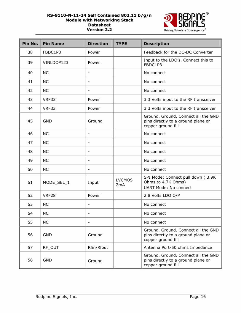
38 FBDC1P3 Power Feedback for the DC-DC Converter
39 VINLDOP123 Power Input to the LDO’s. Connect this to
FBDC1P3.
40 NC - No connect
41 NC - No connect
42 NC - No connect
43 VRF33 Power 3.3 Volts input to the RF transceiver
44 VRF33 Power 3.3 Volts input to the RF transceiver
45 GND Ground
Ground. Ground. Connect all the GND
pins directly to a ground plane or copper ground fill
46 NC - No connect
47 NC - No connect
48 NC - No connect
49 NC - No connect
50 NC - No connect
51 MODE_SEL_1 Input LVCMOS
2mA
SPI Mode: Connect pull down ( 3.9K
Ohms to 4.7K Ohms)
UART Mode: No connect
52 VRF28 Power 2.8 Volts LDO O/P
53 NC - No connect
54 NC - No connect
55 NC - No connect
56 GND Ground
Ground. Ground. Connect all the GND
pins directly to a ground plane or copper ground fill
57 RF_OUT Rfin/Rfout Antenna Port-50 ohms Impedance
58 GND
Ground
Ground. Ground. Connect all the GND
pins directly to a ground plane or copper ground fill

Redpine Signals, Inc. Page 17
RRSS--99111100--NN--1111--2244 SSeellff CCoonnttaaiinneedd 880022..1111 bb//gg//nn
MMoodduullee wwiitthh NNeettwwoorrkkiinngg SSttaacckk
DDaattaasshheeeett
VVeerrssiioonn 22..22
Notes:
Please contact Redpine Signals for application notes or for customization
of a solution.
Redpine Signals, Inc. Page 18
RRSS--99111100--NN--1111--2244 SSeellff CCoonnttaaiinneedd 880022..1111 bb//gg//nn
MMoodduullee wwiitthh NNeettwwoorrkkiinngg SSttaacckk
DDaattaasshheeeett
VVeerrssiioonn 22..22
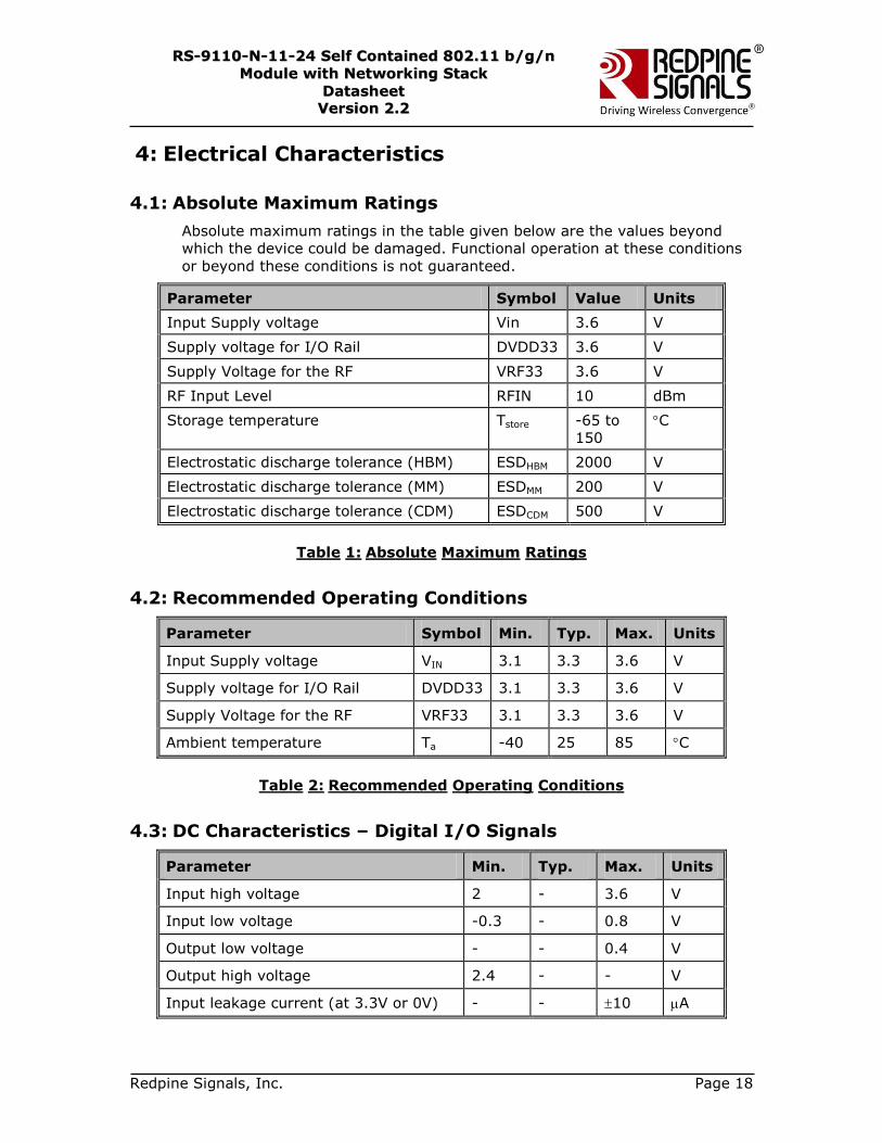
4: Electrical Characteristics
4.1: Absolute Maximum Ratings
Absolute maximum ratings in the table given below are the values beyond
which the device could be damaged. Functional operation at these conditions
or beyond these conditions is not guaranteed.
Parameter Symbol Value Units
Input Supply voltage Vin 3.6 V
Supply voltage for I/O Rail DVDD33 3.6 V
Supply Voltage for the RF VRF33 3.6 V
RF Input Level RFIN 10 dBm
Storage temperature Tstore -65 to
150
C
Electrostatic discharge tolerance (HBM) ESDHBM 2000 V
Electrostatic discharge tolerance (MM) ESDMM 200 V
Electrostatic discharge tolerance (CDM) ESDCDM 500 V
Table 1: Absolute Maximum Ratings
4.2: Recommended Operating Conditions
Parameter Symbol Min. Typ. Max. Units
Input Supply voltage VIN 3.1 3.3 3.6 V
Supply voltage for I/O Rail DVDD33 3.1 3.3 3.6 V
Supply Voltage for the RF VRF33 3.1 3.3 3.6 V
Ambient temperature Ta -40 25 85 C
Table 2: Recommended Operating Conditions
4.3: DC Characteristics – Digital I/O Signals
Parameter Min. Typ. Max. Units
Input high voltage 2 - 3.6 V
Input low voltage -0.3 - 0.8 V
Output low voltage - - 0.4 V
Output high voltage 2.4 - - V
Input leakage current (at 3.3V or 0V) - - 10 A
Redpine Signals, Inc. Page 19
RRSS--99111100--NN--1111--2244 SSeellff CCoonnttaaiinneedd 880022..1111 bb//gg//nn
MMoodduullee wwiitthh NNeettwwoorrkkiinngg SSttaacckk
DDaattaasshheeeett
VVeerrssiioonn 22..22
Parameter Min. Typ. Max. Units
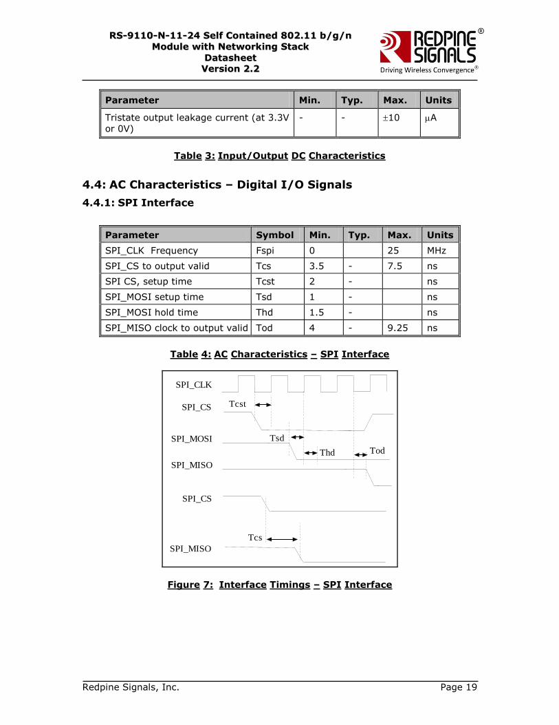
Tristate output leakage current (at 3.3V
or 0V)
- - 10 A
Table 3: Input/Output DC Characteristics
4.4: AC Characteristics – Digital I/O Signals
4.4.1: SPI Interface
Parameter Symbol Min. Typ. Max. Units
SPI_CLK Frequency Fspi 0 25 MHz
SPI_CS to output valid Tcs 3.5 - 7.5 ns
SPI CS, setup time Tcst 2 - ns
SPI_MOSI setup time Tsd 1 - ns
SPI_MOSI hold time Thd 1.5 - ns
SPI_MISO clock to output valid Tod 4 - 9.25 ns
Table 4: AC Characteristics – SPI Interface
SPI_CLK
SPI_CS
SPI_MOSI
SPI_MISO
Tcst
Tod
Tsd
Thd
Tcs
SPI_CS
SPI_MISO
Figure 7: Interface Timings – SPI Interface
Redpine Signals, Inc. Page 20
RRSS--99111100--NN--1111--2244 SSeellff CCoonnttaaiinneedd 880022..1111 bb//gg//nn
MMoodduullee wwiitthh NNeettwwoorrkkiinngg SSttaacckk
DDaattaasshheeeett
VVeerrssiioonn 22..22
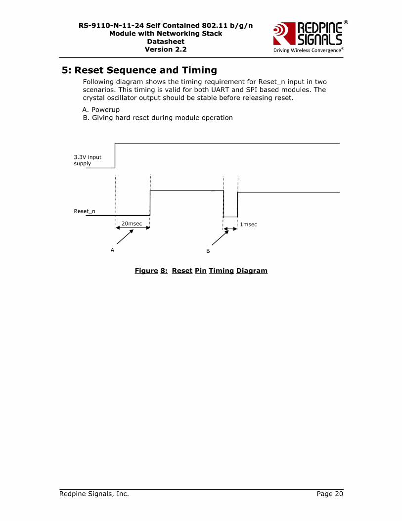
5: Reset Sequence and Timing Following diagram shows the timing requirement for Reset_n input in two
scenarios. This timing is valid for both UART and SPI based modules. The
crystal oscillator output should be stable before releasing reset.
A. Powerup
B. Giving hard reset during module operation
Figure 8: Reset Pin Timing Diagram
3.3V input supply
20msec
A
1msec
B
Reset_n
Redpine Signals, Inc. Page 21
RRSS--99111100--NN--1111--2244 SSeellff CCoonnttaaiinneedd 880022..1111 bb//gg//nn
MMoodduullee wwiitthh NNeettwwoorrkkiinngg SSttaacckk
DDaattaasshheeeett
VVeerrssiioonn 22..22
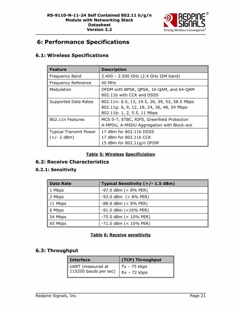
6: Performance Specifications
6.1: Wireless Specifications
Feature Description
Frequency Band 2.400 – 2.500 GHz (2.4 GHz ISM band)
Frequency Reference 40 MHz
Modulation OFDM with BPSK, QPSK, 16-QAM, and 64-QAM
802.11b with CCK and DSSS
Supported Data Rates 802.11n: 6.5, 13, 19.5, 26, 39, 52, 58.5 Mbps
802.11g: 6, 9, 12, 18, 24, 36, 48, 54 Mbps
802.11b: 1, 2, 5.5, 11 Mbps
802.11n Features MCS 0-7, STBC, RIFS, Greenfield Protection
A-MPDU, A-MSDU Aggregation with Block-ack
Typical Transmit Power
(+/- 2 dBm)
17 dBm for 802.11b DSSS
17 dBm for 802.11b CCK
15 dBm for 802.11g/n OFDM
Table 5: Wireless Specificiation
6.2: Receive Characteristics
6.2.1: Sensitivity
Data Rate Typical Sensitivity (+/- 1.5 dBm)
1 Mbps -97.0 dBm (< 8% PER)
2 Mbps -93.0 dBm (< 8% PER)
11 Mbps -88.9 dBm (< 8% PER)
6 Mbps -91.0 dBm (<10% PER)
54 Mbps -75.0 dBm (< 10% PER)
65 Mbps -71.0 dBm (< 10% PER)
Table 6: Receive sensitivity
6.3: Throughput
Interface (TCP) Throughput
UART (measured at 115200 bauds per sec)
Tx – 75 kbps
Rx – 72 kbps

Redpine Signals, Inc. Page 22
RRSS--99111100--NN--1111--2244 SSeellff CCoonnttaaiinneedd 880022..1111 bb//gg//nn
MMoodduullee wwiitthh NNeettwwoorrkkiinngg SSttaacckk
DDaattaasshheeeett
VVeerrssiioonn 22..22
Interface (TCP) Throughput
SPI Tx – 8 Mbps (TCP), 9
Mbps (UDP)
Rx – 5 Mbps (TCP), 6 Mbps (UDP)
The numbers are the actual application throughputs. For physical data rates,
please refer to the table Wireless Specificiation .
6.4: Range
Range varies with the conditions under with wireless communication is
sought. For large office environments, in the presence of obstacles, a range of
over 30 metres is observed, while in open, line-of-sight environments, over
300 metres is observed.
6.5: Standards Compliance
RS9110-N-11-24 is compliant with the requirements of IEEE 802.11b,
802.11g, 802.11j, and 802.11n that include the following:
Transmit Spectral Mask
Transmit Center Frequency Leakage
Transmit Center Frequency Tolerance
Symbol Clock Frequency Tolerance
Transmit Constellation error
Receiver Adjacent Channel Interference Rejection
Receiver Non-adjacent Channel Rejection
Receiver Minimum Input Level
Receiver Maximum Input Level
Redpine Signals, Inc. Page 23
RRSS--99111100--NN--1111--2244 SSeellff CCoonnttaaiinneedd 880022..1111 bb//gg//nn
MMoodduullee wwiitthh NNeettwwoorrkkiinngg SSttaacckk
DDaattaasshheeeett
VVeerrssiioonn 22..22
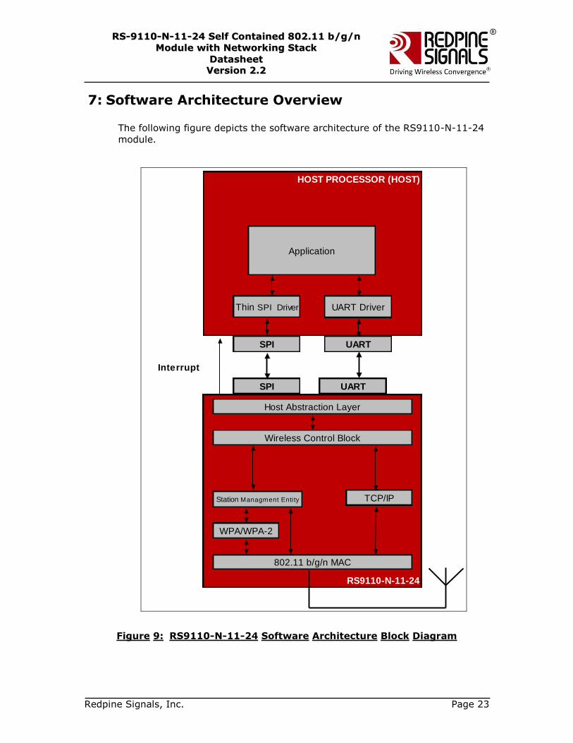
7: Software Architecture Overview
The following figure depicts the software architecture of the RS9110-N-11-24
module.
SLIP
UART
HOST PROCESSOR (HOST)
RS9110-N-11-24
Host Abstraction Layer
Station Managment Entity
802.11 b/g/n MAC
TCP/IP
Wireless Control Block
SPI
WPA/WPA-2
UART DriverThin SPI Driver
UARTSPI
Application
Interrupt
Figure 9: RS9110-N-11-24 Software Architecture Block Diagram
Redpine Signals, Inc. Page 24
RRSS--99111100--NN--1111--2244 SSeellff CCoonnttaaiinneedd 880022..1111 bb//gg//nn
MMoodduullee wwiitthh NNeettwwoorrkkiinngg SSttaacckk
DDaattaasshheeeett
VVeerrssiioonn 22..22
As shown in the figure above, the RS9110-N-11-24 module is integrated with
the Host using either UART or SPI interfaces. The transmission and reception
of the data to/from the Host depends on the interface used to connect the
module as briefed below.
UART mode:
The Host transmits/receives raw data using UART interface when the RS9110-
N-11-24 module is configured for UART mode. The access to the TCP/IP stack
in the Wi-Fi module through the UART is provided through AT commands.
SPI mode:
Host transmits/receives raw data using SPI interface when the RS9110-N-11-
24 module is configured for SPI mode. A thin driver on the Host takes care of
interacting with the Wi-Fi module through the SPI Host interface.
The following sections explain in brief the various components illustrated in
Figure 9.
7.1: Host
The Host is any system that has applications being executed and either a
UART or SPI interface.
7.1.1: UART
The UART on the Host side provides an interface for the host to access the
Wi-Fi module. UART is used to configure various parameters of the RS9110-
N-11-24 module and also to send and receive data over the network by
accessing the TCP/IP stack in the RS9110-N-11-24 module.
7.1.2: SPI
The SPI on the Host side provides an interface for the host to access the Wi-Fi
module. SPI on the Host acts as the master.
7.1.3: Thin SPI Driver
The SPI driver on the Host is a thin driver through which the applications
interact with the Wi-Fi module. The SPI driver uses the SPI host controller
driver on the Host to send/receive the data to/from the RS9110-N-11-24
module and also to configure the same over the SPI interface.
7.2: RS9110-N-11-24
The RS9110-N-11-24 module incorporates Wi-Fi, TCP/IP, DHCP, ARP, etc. to
act as a WLAN device. It handles all the network connectivity functions. The
following sections describe the software components of the RS9110-N-11-24
module in brief.
7.2.1: SPI
The SPI on the RS9110-N-11-24 acts the SPI slave. It is a standard 4-wire
SPI and can support a maximum frequency of 25MHz.
7.2.2: UART
The UART on the RS9110-N-11-24 module is the physical interface which
transmits/receives the data from the Host. It supports variable baud rates

Redpine Signals, Inc. Page 25
RRSS--99111100--NN--1111--2244 SSeellff CCoonnttaaiinneedd 880022..1111 bb//gg//nn
MMoodduullee wwiitthh NNeettwwoorrkkiinngg SSttaacckk
DDaattaasshheeeett
VVeerrssiioonn 22..22
from 9600 to 3686400 bps. There is support for AT commands to configure
and operate the module through UART interface.
7.2.3: Host Abstraction Layer (HAL)
The HAL abstracts the lower layers in the host interface with which the
RS9110-N-11-24 module is connected. The HAL interacts with the Wireless
Control Block layer for the processing of the frames obtained from or destined
to the Host.
7.2.4: Wireless Control Block (WCB)
The data from/to the Host is classified as Wi-Fi specific frames and TCP/IP
specific frames. The WCB layer processes the frame obtained and acts
accordingly. The functionality of the WCB module depends on the type of the
frame and the direction of the frame (in case of TCP/IP) as described below.
7.2.4.1: TCP/IP Control frames
If the frames from the host are interpreted as TCP/IP specific frames then the
WCB interacts with the TCP/IP stack.
7.2.5: Station Management Entity (SME)
The SME is the core layer, which manages the Wi-Fi connectivity. The SME
maintains the state machine to detect the activity on the Wi-Fi network and
indicates to the user accordingly. It also performs re-association to the
configured access point in Infrastructure mode. It interacts with the WPA
supplicant if Security is enabled in the Wi-Fi network.
7.2.6: WPA Supplicant
The WPA supplicant is used to initiate the 802.1x/EAP authentication if WPA2-
PSK is used as the security parameter. It also plays a major part in
performing the 4-way handshake to derive the PTK in WPA2-PSK modes.
7.2.7: Power Save Modes
The RS9110-N-11-2X module supports three power modes. The Host can
switch among the power modes depending on the Wi-Fi connection status as
defined in this section.
7.2.7.1: Power mode 0
In this mode, power save is disabled in the RS9110-N-11-2X module. The
module will be in Power Mode 0 by default.
7.2.7.2: Power mode 1
The RS9110-N-11-2X module powers off the Baseband, RF and also the Core
Control block in this mode. To power off the Core Control block, the RS9110-
N-11-2X module sends request to Host for permission to sleep.
Once the permission is received the Core Control block is powered off. The
Host has to wait for the module to wakeup based on the timer that is
configured by the Host, before it can transmit any packets.
The functioning of the module in this mode depends on the connection status
as explained below
Redpine Signals, Inc. Page 26
RRSS--99111100--NN--1111--2244 SSeellff CCoonnttaaiinneedd 880022..1111 bb//gg//nn
MMoodduullee wwiitthh NNeettwwoorrkkiinngg SSttaacckk
DDaattaasshheeeett
VVeerrssiioonn 22..22
1. Before Wi-Fi connection
In this state, the module is configured with a sleep timer. Once the
timer expires, the module powers on the Core Control block and
sends the request for sleep permission to the Host again. On
getting permission the Host, the module will power off the Core
Control block for another interval of the sleep period.
If the host wants to perform any Wi-Fi related activity like scanning
or joining networks, it has to switch to Power Mode 0. After a
connection is established, it can switch back to Power Mode 1 or 2.
2. After Wi-Fi Connection
In this state, the RS9110-N-11-2X module periodically wakes up to
receive beacons from the Access Point (AP). If there is no data to
be transmitted or received to/from the Access Point, it powers off
the Baseband and RF components and requests the Host
permission to turn off the Core Control block. On receiving
permission from the Host, the module goes to sleep and wakes up
before the next beacon comes.
7.2.7.3: Power mode 2
The RS9110-N-11-2X module powers off the Baseband and RF components in
this mode. The Core Control block interacting with the Host is always
functional in this mode. Hence, the module can receive commands from the
host at any time.
NOTE: The average current consumption in Power Mode 2 is higher than
Power Mode 1.
The functioning of the module in this mode depends on the connection status
as explained below
1. Before Wi-Fi connection
If this power mode is enabled before the Wi-Fi connection is
established, the module powers off the Baseband and RF
components until the Host reconfigures the module to Power Mode
0.
If the host wants to perform any Wi-Fi related activity like scanning
and joining networks, it has to switch to Power Mode 0. This can be
done at any time during the operation. The Host can switch back to
Power Modes 1 or 2 after the Wi-Fi connection is established.
2. After Wi-Fi Connection
In this state, the RS9110-N-11-2X module gets information from
the Access Point to which it is connected for any buffered data at
every beacon. If there is no data to be transmitted or received
to/from the Access Point, it powers off the Baseband and RF
components.

Redpine Signals, Inc. Page 27
RRSS--99111100--NN--1111--2244 SSeellff CCoonnttaaiinneedd 880022..1111 bb//gg//nn
MMoodduullee wwiitthh NNeettwwoorrkkiinngg SSttaacckk
DDaattaasshheeeett
VVeerrssiioonn 22..22
8: Ordering Information
Contact Information:
For additional information, please contact Sales at Redpine Signals, Inc.
Redpine Signals, Inc.
2107 North First Street, Suite 680,
San Jose, CA 95131 USA
Phone: +1 408 748 3385
E-mail: [email protected]
Website: http://www.redpinesignals.com/
Device Ordering Information:
The following table lists the part numbers to be used for ordering modules or
evaluation boards (EVB). Redpine can create and provide customized
firmware based on user requirements.
Device Number Description Packaging Qualification
RS9110-N-11-24 Part with UART1
as Host interface
Tray -40 C to +85 C
RS9110-N-11-24-02 Part with SPI as
Host interface
Tray -40 C to +85 C
RS9110-N-11-24-EVB Evaluation board
with UART as Host interface
Tray -40 C to +85 C
RS9110-N-11-24-02-EVB Evaluation board
with SPI as Host
interface
Tray -40 C to +85 C
Table 7: Device Ordering Information
Collateral:
The following documentation and software are available along with the
RS9110-N-11-24 modules or Evaluation Boards (EVB).
Embedded firmware for WLAN and TCP/IP stack
AT Command Interface and SPI driver software
Reference Schematics and Layout Guidelines - Describes hardware
schematics to operate the module in UART and SPI modes
Programming Reference Manual - Describes how to operate the module in
UART and SPI modes
Evaluation Board (EVB) and related user guides
1 TKIP mode of security is not supported in the UART interface module.
Redpine Signals, Inc. Page 28
RRSS--99111100--NN--1111--2244 SSeellff CCoonnttaaiinneedd 880022..1111 bb//gg//nn
MMoodduullee wwiitthh NNeettwwoorrkkiinngg SSttaacckk
DDaattaasshheeeett
VVeerrssiioonn 22..22
9: Command Reference (AT commands and SPI commands)
AT Command Set (for UART interface) and SPI command set (for SPI interface)
supports the following in RS9110-N-11-XX module. This is an indicative list and not a
full list. The full list of commands is available in the Programming Reference Manual.
i. Configure the band to 2.4GHz
ii. Initialize MAC and Baseband
iii. Scan for avialable networks
iv. Join an available network in infrastructure or ad-hoc modes
v. Configure IP addresses
vi. Open and close TCP and UDP sockets Send and receive data
***