Embed Size (px)
Citation preview
E.G.S.P ENGINEERING COLLEGEDEPARTMENT OF MCA
MODEL III KEYSUBJECT : COMPUTER ORGANIZATION MAX. MARKS :100SUB.CODE : MC7101 TIME : 3HRS
PART-A (10 X 2= 20)
1. Convert -14 and -10 to a 5bit signed 2’s complement binary numbers and add them. State whether or not overflow occurs. Ans: 2’s complement of -14 is 10010 2’s complement of -10 is 10110
Sum is 1 01000 Hence overflow occurs2. Simplify the following Boolean functions to a minimum number of literals:
a) (x+y)(x+y’) Ans: xx+xy’+xy+yy’
= x+x(y+y’)+yy’ = x+x+0
= xb) y(wz’+wz)+xy
Ans: yw(z’+z) +xy = yw+xy
= y(w+x)3. Differentiate combinational and sequential circuits Ans: Combinational:
It is a circuit made up of logic gates and accepts input and generates the output based on the present input alone without regard to the previous input Sequential:
It is a circuit made up of logic gates and flip flops whose output at any time is determined by the present combination of input as well as previous input4. Write the general syntax of r’s and (r-1)’s complement
Ans:General syntax of r’s complementCovert all zero into 1 and 1 into 0Eg: 10010101 => 01101010General syntax of r-1’s complement1.Covert all zero into 1 and 1 into 02. add 1 to the result of step 1 Eg: 1) 10010101 => 01101010 2) 01101011
5. What are the contents of an instruction register? Ans:
Instruction register consists of instruction which is currently being executed 6. What does locality of reference mean? Ans: Locality of reference, also known as the principle of locality, is the phenomenon that many instructions in localized areas of the program are executed repeatedly during some time period , and the remainder of the program accessed infrequently. There are two basic types of

locality of reference. Temporal locality means that a recently executed instructions is likely to be executed very
soon. Spatial locality means that instructions in close proximity to a recently executed instruction are
also likely to be executed soon. 7. What is the function of MAR?
Ans: MAR is the memory address register which is loaded with the content of PC thus points to the memory location
8. What is data path?Ans:The registers, the ALU, and the interconnecting bus are collectively referred to as the datapath.
9. What is virtual memory?Ans:virtual memory is a technique which gives an application program the impression that it has contiguous working memory in the computer system. Techniques that automatically move program and data blocks into the physical main memory when they are required the execution are called virtual-memory technique.
10.Write the need of cache memory Ans:
It is a small, fast memory used to have active segments of a program, thus total execution time can be reduced significantly
PART-B (5 X 16=80)
11.a) Simplify the Boolean function F together with the don’t care conditions F(W,X,Y,Z) = ∑ (0,1,2,3,7,8,10) D (W, X, Y, Z) = ∑ (5, 6, 11,15)Ans:
1. construct the K-map2. plot the minterms3. plot the don’tcares4. group the minterms as octets, quads,pairs and singles whichever combination is possible5. derive the simplified Boolean function
(OR) b. i) Write a short note on flip-flop with its diagram and excitation table (10)
Ans: Binary memory cell capable of storing 1 bit or information (either stores a 0 or a 1)
A flip-flop has a clocked input and can only change at certain times specified by the type of clocking. So a flip-flop could be called a clocked latch. .
Flip – flops - There are 4 primary types of flip-flops 1. SR flip-flop2. D flip-flop3. JK flip-flop4. T flip-flop
ii) Simplify the following Boolean functions to a minimum number of literals: (6)
a) x’y’+xy+x’y
Ans:
= 1+ x’y [ since x+x’ = 1]
= 1[since 1+x’y = 1]
b) (x+y)(x+y)’
Ans:
= (x+y)(x’y’)
= xx’y+x’y’y[ since xx’=0]
= 0
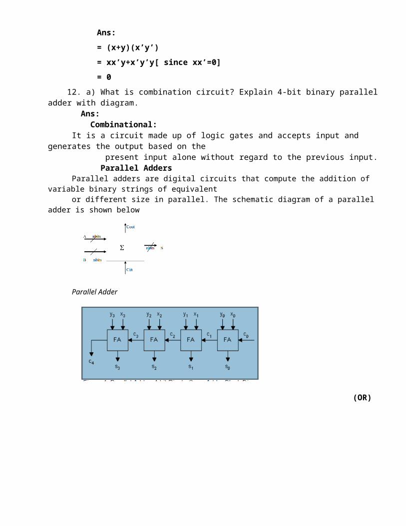
12. a) What is combination circuit? Explain 4-bit binary parallel adder with diagram. Ans: Combinational:
It is a circuit made up of logic gates and accepts input and generates the output based on the present input alone without regard to the previous input. Parallel Adders
Parallel adders are digital circuits that compute the addition of variable binary strings of equivalent or different size in parallel. The schematic diagram of a parallel adder is shown below
Parallel Adder
(OR)
\
b) Explain the design of sequential circuit with necessary steps.
Design of Sequential Circuits
The design of a synchronous sequential circuit starts from a set of specifications and culminates in a logic diagram or a list of Boolean functions from which a logic diagram can be obtained. In contrast to a combinational logic, which is fully specified by a truth table, a sequential circuit requires a state table for its specification. The first step in the design of sequential circuits is to obtain a state table or an equivalence representation, such as a state diagram.
A synchronous sequential circuit is made up of flip-flops and combinational gates. The design of the circuit consists of choosing the flip-flops and then finding the combinational structure which, together with the flip-flops, produces a circuit that fulfils the required specifications. The number of flip-flops is determined from the number of states needed in the circuit.
The recommended steps for the design of sequential circuits are set out below.
13.a) Explain about generic addressing modes with example for each type. Ans: The strategy to identify WHERE the operand is located.
Effective Address (definition):• Actual location of operand to be used by the instruction:
Types: Immediate addressing mode Direct addressing mode Indirect addressing mode Register addressing mode Register indirect addressing mode Displacement addressing mode

1) Relative addressing2) Base register addressing3) Indexing addressing
(OR) b) Explain about the design of Arithmetic Logic Unit (ALU) Ans:
arithmetic logic unit (ALU) is a digital circuit that performs arithmetic and logical operations. The ALU is a fundamental building block of the central processing unit (CPU) of a computer.
Explain all arithmetic operations Explain all logical operations Draw the necessary diagram
14.a) With neat sketch explain basic organization of a microprogramed control unit. A microprogrammed control unit is a relatively simple logic circuit that is capable of (1) sequencing through microinstructions and (2) generating control signals to execute each microinstructionMicroprogram are stored in microprogram memory and the execution is controlled by microprogram counter ( PC ) .Microprogram consists of microinstructions which are nothing but the strings of 0’s and 1’s . In a particular instance ,we read the contents of one location of microprogram memory , which is nothing but a microinstruction . Each output line ( data line ) of microprogram memory corresponds to one control signal. If the contents of the memory cell is ) , it indicates that the signal is to generated and if the contents of memory cell is 1 , it indicates that generate that control signal at that instant of time.Control Word (CW) : Control word is defined as a word whose individual bits represent the various control signal. Therefore each of the control steps in the control sequence of an instruction defines a unique combination of 0s and 1s in the CW.
A sequence of control words ( CWs ) corresponding to the control sequence of a machine instruction constitutes the microprogram for that instruction.
The individual control words in this microprogram are referred to as microinstructions.
The microprograms corresponding to the instruction set of a computer are stored ina aspecial memory which will be referred to as the microprogram memory. The control words related to an instructions are stored in microprogram memory.
The control unit can generate the control signals for any instruction by sequencially reading the CWs of the corresponding microprogram from the microprogram memory.To read the control word sequentially from the microprogram memory a microprogram counter ( PC ) is needed.
The basic organization of a microprogrammed control unit is shown in the figure.

Basic organization of a microprogrammed control
The “starting address generator “ block is responsible for loading the starting address of the microprogram into the PC everytime a new instruction is loaded in the IR.
The PC is then automatically incremented the clock, and it reads the successive microinstruction from memory . Each microinstruction basically provides the required control signal at that time step. The microprogram counter ensures that the control signal will be delivered to the various parts of the CPU in correct sequence.
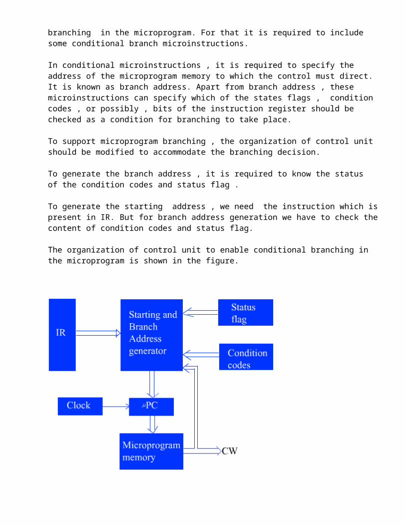
We have some instructions whose execution depends on the status of condition codes and status flag , as for example , the branch instruction. During branch instruction execution it is required to take the decision between the alternative action.
To handle such type of instructions with microprogrammed control , the design of control unit is based on the concept of conditional branching in the microprogram. For that it is required to include some conditional branch microinstructions.
In conditional microinstructions , it is required to specify the address of the microprogram memory to which the control must direct. It is known as branch address. Apart from branch address , these microinstructions can specify which of the states flags , condition codes , or possibly , bits of the instruction register should be checked as a condition for branching to take place.
To support microprogram branching , the organization of control unit should be modified to accommodate the branching decision.
To generate the branch address , it is required to know the status of the condition codes and status flag .
To generate the starting address , we need the instruction which is present in IR. But for branch address generation we have to check the content of condition codes and status flag.

The organization of control unit to enable conditional branching in the microprogram is shown in the figure.
The control bits of the microinstructions word which specify the branch conditions and address are fed to the “ Starting and branch address generator “ block.
This block performs the function of loading a new address into the PC when the condition of branch instruction is satisfied.
In a computer program we have seen that execution of every instruction consists of two part – fetch phase and execution phase of the instruction. It is also observed that the fetch phase of all instruction is same.
In microprogrammed controlled control unit , a common microprogram is used to fetch the instruction. This microprogram is stored in a specific location and execution of each instruction start from that memory location.
At the end of fetch microprogram , the starting address generator unit calculate the appropriate starting address of the microprogram for the instruction which is currently present in IR. After the PC controls the execution of microprogram which generates the appropriate control signal in proper sequence.
During the execution of a microprogram , the PC is always incremented everytime a new microinstruction is fetched from the microprogram memory , except in the following situations :
1. When an End instruction is encountered , the PC is loaded with the address of the first CW in the microprogram for the instruction fetch cycle.

2. When a new instruction is loaded into the IR , the PC is loaded with the starting address of the microprogram for that instruction.
3. When a branch microinstruction is encountered , and the branch condition is satisfied , the PC is loaded with the branch address.
Let us examine the contents of microprogram memory and how the microprogram of each instruction is stored or organized in microprogram memory.
Consider the two example that are used in our previous lecture .
First exam is the control sequence for execution of the instruction “ Add contents of memory location addressed in memory direct mode to register RI”
Step Action
1. PCout , MARin Read , Clear Y, set carry_in to ALU, Add , Zin
2. Zout , PCin , Wait for MFC
3. MDRout , IRin
4. Address_field_of_IRow , MARin , Read
5. RIout , Yin , Wait for MFC
6. MDRout , Add , Zin
7. Zout , RIin
8. End
(OR) b) Write short notes: i) Prefetching micro instructions ii) Emulation iii) Hazard (4+4+8)
Hazard:
i)Prefetching micro instructions:
ii)Emulation: It is a way of simulating the function of one machine into another. For example M1 is a machine with instruction set I1 and machine M2 is the upgraded version of M1 with instruction set I2. Then a program written for M1 if it could be executed in M2, we can say that M2 emulates M1
iii) Hazards are problems with the instruction pipeline in central processing unit (CPU) microarchitectures that potentially result in incorrect computation. There are typically three types of hazards:
data hazards structural hazards control hazards (Instruction hazard)
1. Structural hazards. A structural hazard occurs when a single hardware component is needed by more than one instruction in the pipeline. For example, if there is a single ALU, which is used by two different pipeline stages, it will not be possible to have two instructions perform those two stages at the same time. In general, the problem here is insufficient parallelism in the data path. We need to add hardware components so that components are not shared between stages.
2. Data hazards. A data hazard occurs when an instruction depends on the result of a prior instruction, but that result is not available when needed because the prior instruction has not yet completed.
3. Control hazards. A control hazard occurs as a result of an instruction (e.g., a branch) which changes the program counter. The result is that some instructions already in the pipeline may need to be invalidated, thus causing lost cycles. Control hazards can be caused by branches or interrupts
15.a) i) What are different memory technology? Explain memory hierarchy in detail (8+8) ROM
i. PROMii. EPROM
iii. EEPROM RAM
i. SRAMii. DRAM)
memory hierarchy diagram with explanation Processor
Registers
Cache L1
Cache L2
M ainm em ory
secondarystoragem em ory
increasingsize
increasingspeed
increasingcost per bit

ii) I/O interface Ans:
Input interface (how keyboard is connected to a processor) output interface (how printer is connected to a processor)
(OR) b. Define virtual memory. Explain the working principles of virtual memory
definition address translation with neat sketch
E.G.S.P ENGINEERING COLLEGEDEPARTMENT OF MCA
MODEL III KEYSUBJECT : COMPUTER ORGANIZATION MAX. MARKS :100SUB.CODE : MC7101 TIME : 3HRS
PART-A (10 X 2= 20)
1. Convert decimal 41 to binary. Ans:
(41)10 = (101001)2
2. Write the purpose of Boolean algebra.Ans: Boolean algebra is used primarily to arrange logic gates to accomplish the desired tasks. Boolean algebra also enables the engineers to achieve the desired output by using the fewest number of logic gates thus reduces the space, weight, and cost involved in the design of equipments.
3. Differentiate between encoder and decoder.Ans:Encoder is the reverse of a decoder. In a decoder it has n input lines and 2 n output lines, but in an encoder it has 2 n input lines and n output lines.
4. How many address lines and I/O data lines are needed in 2K *16 memory unit?Ans:15 address lines and 2 lines for power and ground connection
5. List the major characteristics of a RISC processor. Ans:
32-bit address 32-bit processor registers Supports both little and big endian memory addressing

Memory is accessed only by load and store instructions6. What is relative addressing mode?
Ans:The effective address (EA) is determined by the index mode using PC. EA gives the location of the operand.Eg:Branch >0 LOOP
7. What do you mean by MDR? ExplainAns:MDR stands for memory data register. It is used to hold the data or instruction loaded from the data bus.
8. Define register file.Ans:All general purpose registers belong to a processor are grouped together and referred as register file
9. What is the difference between associative and set associative mapping in cache memory?Ans:Associative mapping is a technique used to place a main memory block into any cache block whichever block is free.Set associative mapping is basically a good compromise between direct mapping and fully associative mapping. It builds on the strengths of both: namely, the easy control of the direct mapped cache and the more flexible mapping of the fully associative cache.
In set associative mapping, cache is divided into a number of smaller direct-mapped areas called sets (v), with each set holding a number of blocks (k).The cache is then described in the number of blocks each set contains. If a set can hold X blocks, the cache is referred to as an X-way set associative cache. A main memory block can be stored in any one of the k blocks in a set such that cache set number = j modulo v (where j is the main memory block number).
10. Write the working principle of DMA.It is used to transfer block of data between any external device and the main memory without much intervention from the processor.
PART-B (5X16=80)
11.a) Write a note on the following with example : (4x4=16) a) Boolean algebra Ans: A Boolean Algebra is a mathematical system consisting of a set of elements B, two binary operations OR (+) and AND (•), a unary operation NOT ('), an equality sign (=) to indicate equivalence of expressions, and parenthesis to indicate the ordering of the operations
b) Truth tableAns: A truth table shows how a logic circuit's output responds to various combinations of the inputs, using logic 1 for true and logic 0 for false. All permutations of the inputs are listed on the left, and the output of the circuit is listed on the right. The desired output can be achieved by a combination of logic gates. A truth table for two inputs is shown, but it can be extended to any number of inputs. The input columns are usually constructed in the order of binary counting with a number of bits equal to the number of inputs.

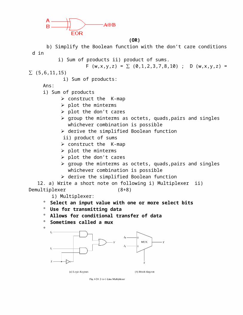
c) EX-OR gate Ans: EXOR gate
The 'Exclusive-OR' gate is a circuit which will give a high output if either, but not both, of its two inputs are high. An encircled plus sign ( ) is used to show the EOR operation.
c) Logic diagramAns:A graphical representation of the logic design or a portion thereof; displays the existence of functional elements and the paths by which they interact with one anotherEg:
(OR) b) Simplify the Boolean function with the don’t care conditions d in i) Sum of products ii) product of sums.
F (w,x,y,z) = ∑ (0,1,2,3,7,8,10) ; D (w,x,y,z) = ∑ (5,6,11,15) i) Sum of products:
Ans:i) Sum of products
construct the K-map plot the minterms plot the don’t cares group the minterms as octets, quads,pairs and singles whichever combination is
possible derive the simplified Boolean function
ii) product of sums construct the K-map plot the minterms plot the don’t cares

group the minterms as octets, quads,pairs and singles whichever combination is possible
derive the simplified Boolean function 12. a) Write a short note on following i) Multiplexer ii) Demultiplexer (8+8) i) Multiplexer:
° Select an input value with one or more select bits° Use for transmitting data° Allows for conditional transfer of data° Sometimes called a mux°
ii) Demultiplexer:The opposite of the multiplexer circuit, logically enough, is the demultiplexer. This circuit takes a single data input and one or more address inputs, and selects which of multiple outputs will receive the input signal. The same circuit can also be used as a decoder, by using the address inputs as a binary number and producing an output signal on the single output that matches the binary address input
(OR) b) Define Flip-Flop. Explain about various types of flip-flops
Ans: Binary memory cell capable of storing 1 bit or information (either stores a 0 or a 1)
A flip-flop has a clocked input and can only change at certain times specified by the type of clocking. So a flip-flop could be called a clocked latch. .
Flip – flops - There are 4 primary types of flip-flops o SR flip-flopo D flip-flopo JK flip-flopo T flip-flop

13.a) Compare the architecture of the machines RISC and CISC Ans:Register organization of RISC and CISC CISC RISC
Emphasis on hardware Emphasis on software
Includes multi-clockcomplex instructions
Single-clock,reduced instruction only
Memory-to-memory:"LOAD" and "STORE"incorporated in instructions
Register to register:"LOAD" and "STORE"are independent instructions
Small code sizes,high cycles per second
Low cycles per second,large code sizes
Transistors used for storingcomplex instructions
Spends more transistorson memory registers
(OR) b) Explain the sequence of elementary operations required to execute one complete instruction
To execute one complete instruction:o Fetch the instructiono Fetch the first operando Perform the additiono Load the result into R1Eg: ADD (R3), R1
Control sequence for execution of the instruction ADD (R3), R1
Step Action1. PCout , MARin Read , Select4, Add , Zin2. Zout , PCin , Yin, Wait for MFC3. MDRout , IRin4. R3out, MARin Read5. R1out, Yin,WMFC6. MDRout , SelectY, Add, Zin7. Zout , R1in, End
14.a) How the control signals send through hardwired control unit? Explain it with neat diagram.To execute instructions, the processor must have some means of generating the control signals
needed in the proper sequence.Two categories:
o hardwired controlo microprogrammed control
Hardwired system can operate at high speed; but with little flexibility.

(OR) b) Explain the following: i) Out of order execution ii) operand forwarding (8+8)
i) Out of order execution1. Instruction fetch. 2. Instruction dispatch to an instruction queue (also called instruction buffer) 3. The instruction waits in the queue until its input operands are available. The instruction
is then allowed to leave the queue before earlier, older instructions. 4. The instruction is issued to the appropriate functional unit and executed by that unit. 5. The results are queued. 6. Only after all older instructions have their results written back to the register file, then
this result is written back to the register file. This is called the graduation or retire stage.
Explain the concept with neat sketch
ii) operand forwardingOperand forwarding refer to computer architecture. When concurrent execution in pipelining is stalled
due to a data hazard, then operand forwarding is used. Explain the concept with neat sketch
Figure 7.10. Control unit organization.
CLKClock Control step
IR encoderDecoder/
Control signals
codes
counter
inputs
Condition
External

15.a) What is cache memory? Explain the mapping functions of cache memory Cache is relatively small and expensiveThe basic principle that cache technology is based upon is locality of reference – many instructions in localized areas of the program are executed repeatedly during some time period, and the remainder of the program is accessed relatively infrequently. It manifests itself in 2 ways: temporal locality spatial locality.
Temporal locality means that referenced memory is likely to be referenced again soon. In other words, if the program has referred to an address it is very likely that it will refer to it again.
Spatial locality means that memory close to the referenced memory is likely to be referenced soon. This means that if a program has referred to an address, it is very likely that an address in close proximity will
be referred to soon.
Mapping function:
The mapping function gives the correspondence between main memory blocks and cache lines. Since each cache line is shared between several blocks of main memory (the number of memory blocks >> the number of cache lines There are three types of mapping functions:
direct mapping associative mapping set associative mapping
Explain each mapping technique with example
(OR) b) Explain about Direct memory Access (DMA) with suitable diagram
It is used to transfer block of data between any external device and the main memory without much intervention from the processor.
To transfer data from an I/O device to memory, the DMA controller first sends a Bus Request to the CPU by setting BR to 1. When it is ready to grant this request, the CPU sets it’s Bus grant signal, BG to 1.
The CPU also tri-states it’s address,data, and control lines thus truly granting control of the system buses to the DMA controller.
The CPU will continue to tri-state it’s outputs as long as BR is asserted The DMA controller includes several registers :-
o The DMA Address Register contains the memory address to be used in the data transfer
o The DMA Count Registero Status Register
E.G.S.P ENGINEERING COLLEGEDEPARTMENT OF MCA
MODEL III KEYSUBJECT : COMPUTER ORGANIZATION MAX. MARKS :100SUB.CODE : MC7101 TIME : 3HRS
PART-A (10 X 2 = 20)
1. List the truth table of the function : F= xy+xy’+y’z Ans:
X Y Z XY XY’ Y’Z xy+xy’+y’z
0 0 0 0 0 0 00 0 1 0 0 1 10 1 0 0 0 0 00 1 1 0 0 0 01 0 0 0 1 0 11 0 1 0 1 1 11 1 0 1 0 0 11 1 1 1 0 0 1
2. Perform the following using 1’s complement: i) X-Y ii) Y-X where X=1010100 and Y=1000011Ans:
i) X-Y X = 1010100
1’scomplement of Y = 0111100 X-Y = 10010000ii) Y-X Y = 1000011 1’scomplement of X = 0101011 X-Y = 11011103. Write the difference between Full adder and Half adder.

Half Adder: A half adder (HA) is an arithmetic circuit that is used to add two bits. The block
diagram of HA is shown. It has two inputs and two outputs.
Full Adder: A full adder (FA) is an arithmetic circuit that is used to add three bits. The block diagram of FA is shown. It has three inputs and two outputs.
4. What is register? A processor register (or general purpose register) is a small amount of storage available on the CPU whose contents can be accessed more quickly than storage available elsewhere.5. What is a bus? Write the different lines of bus. Bus is a collection of wires each wire(or line) is capable of carrying bit of information. Types:
a. Data bus b. Address busc. Control bus
6. Given the 16-bit value 0011 0101 1100 1111, what operation must be performed in order to clear to 0 the first 8 bits. Ans: MOV R1, 35CFH AND R1, 00FFH 7. What do you mean by a hazard? Ans: Any condition that stalls the pipeline operation is called hazard. Three types of hazards:
data hazard structural hazard control hazard (Instruction hazard)
8. List the four steps of a pipelined processor Ans:
Fetch phase(F) Decode phase(D) Execute phase(E)

Write phase(W)9. What do you mean by an ISR?Ans:ISR: A section of a computer program or of the operating system that takes control when an interrupt is received and performs the operations required to service the interrupt.
10. List the registers associated with DMA.oThe DMA Address Register contains the memory address to be used in the data transferoThe DMA Count Register which contains no. of bytes to be transferred oStatus Register
PART-B (5 X 16 = 80)
11.a. i) Write a note on karnaugh map Ans:
A Karnaugh Map is a grid-like representation of a truth table. It is really just another way of presenting a truth table, but the mode of presentation gives more insight. A Karnaugh map has zero and one entries at different positions. Each position in a grid corresponds to a truth table entry. Here's an example taken from the voting circuit presented in the lesson on Minterms. The truth table is shown first. The Karnaugh Map for this truth table is shown after the truth table.
A B C V0 0 0 00 0 1 00 1 0 00 1 1 11 0 0 01 0 1 11 1 0 11 1 1 1
ii) Convert (0.6875)10 to binary iii) Convert (0.513)10 to octal (10+3+3) Ans: ( 0.6875)10 to binary = (.1011)2
(0.513)10 to octal = (.4333)2 (OR)

b) Simplify the following Boolean functions using karnaugh map: i) F(w,x,y,z) = ∑ (0,1,2,4,5,6,8,9,12,13,14) (8)
construct the K-map plot the minterms group the minterms as octets, quads,pairs and singles whichever combination is
possible derive the simplified Boolean function
ii) F(a,b,c,d.e) = ∑ (0,2,4,6,9,13,21,23,25,29,31) (8) construct the K-map plot the minterms group the minterms as octets, quads,pairs and singles whichever combination is
possible derive the simplified Boolean function
12.a) Draw the diagram of comparator and explain its working principles in detailo Logical diagram o Working principle (OR)
b) Write a note on following i) Ripple counter ii) Shift Register (8+8)Ripple counter: Counters may be considered as a special register, which counts in a certain count cycle determined by the design of the counting register.Shift Registers:Shift registers are registers that can shift binary bits in one direction or both directions upon the application of clock pulses.
13.a) With a neat timing diagram explain fetching a word from memory Ans:
o MOVE (R1),R2o Actions needed to execute this instruction:
o MAR <- [R1]o Start a Read operation on the memory buso Wait for the MFC response from the memoryo Load MDR from the memory buso R2 <- [MDR]
o Signals to be activated are:o R1out , MARin Read o MDRinE, WMFCo MDRout, R2in
(OR) b) Design the following non binary sequence counter as specified .Treat the unused states as don’t care conditions. Analyze the final circuit to ensure that it is self -correcting Design a counter with the following repeated binary sequence 0, 1,3,5,7. Use T flip-flops
14.a) i) Explain the super scalar operation with its hardware organization (10)o Super scalar design that enables a central processing unit to send several instructions to different
execution units simultaneously, allowing it to execute several instructions in each clock cycle.o super scalar organization diagram

ii) Write a note on Pipeline Hazards (6)
Hazards are problems with the instruction pipeline in central processing unit (CPU) microarchitectures that potentially result in incorrect computation. There are typically three types of hazards:
data hazards structural hazards control hazards (Instruction hazard)
1. Structural hazards. A structural hazard occurs when a single hardware component is needed by more than one instruction in the pipeline. For example, if there is a single ALU, which is used by two different pipeline stages, it will not be possible to have two instructions perform those two stages at the same time. In general, the problem here is insufficient parallelism in the data path. We need to add hardware components so that components are not shared between stages.
2. Data hazards. A data hazard occurs when an instruction depends on the result of a prior instruction, but that result is not available when needed because the prior instruction has not yet completed.
3. Control hazards. A control hazard occurs as a result of an instruction (e.g., a branch) which changes the program counter. The result is that some instructions already in the pipeline may need to be invalidated, thus causing lost cycles. Control hazards can be caused by branches or interrupts
(OR)
b) Write short notes on CPU data path designAns:o Single bus organizationo Multiple bus organization
15.a) Explain the working principle of Associative memory in detail
o Associative memory is also known as content-addressable memory (CAM).
o Associative memory can be directly accessed by the content rather than the physical address in the memory (OR)
b) What is meant by bus arbitration? Explain about types of DMA bus arbitrations• Bus Arbitration – an elaborate system for resolving bus control conflicts and assigning priorities
to the requests for control of the bus.
• Bus Mastering – a method of enabling different device controllers on the bus to ‘talk’ to one an other, without having to go through the CPU.
• DMA(Direct Memory Access) – a method of transferring data from a hard disk to main memory without having to go through the CPU.
• Bus Arbitration Methods• Centralized

Centralized bus arbitration requires hardware (arbiter)that will grant the bus to one of the requesting devices. This hardware can be part of the CPU or it can be a separate device on the motherboard. • Decentralized
Decentralized arbitration there isn't an arbiter, so the devices have to decide who goes next. This makes the devices more complicated, but saves the expense of having an arbiter.