Embed Size (px)
Citation preview

HAL Id: hal-01706735https://hal.archives-ouvertes.fr/hal-01706735
Submitted on 12 Feb 2018
HAL is a multi-disciplinary open accessarchive for the deposit and dissemination of sci-entific research documents, whether they are pub-lished or not. The documents may come fromteaching and research institutions in France orabroad, or from public or private research centers.
L’archive ouverte pluridisciplinaire HAL, estdestinée au dépôt et à la diffusion de documentsscientifiques de niveau recherche, publiés ou non,émanant des établissements d’enseignement et derecherche français ou étrangers, des laboratoirespublics ou privés.
Role of internal demagnetizing field for the dynamics ofa surface-modulated magnonic crystal
M. Langer, F. Röder, R. Gallardo, T. Schneider, S. Stienen, Christophe Gatel,R. Hübner, L. Bischoff, K. Lenz, J. Lindner, et al.
To cite this version:M. Langer, F. Röder, R. Gallardo, T. Schneider, S. Stienen, et al.. Role of internal demagnetiz-ing field for the dynamics of a surface-modulated magnonic crystal. Physical Review B: CondensedMatter and Materials Physics (1998-2015), American Physical Society, 2017, 95 (18), �10.1103/Phys-RevB.95.184405�. �hal-01706735�

arX
iv:1
609.
0034
2v3
[co
nd-m
at.m
trl-
sci]
20
Oct
201
6
The role of the internal demagnetizing field for the dynamics of a magnonic crystal
M. Langer,1, 2 F. Roder,1, 3, 4 R. A. Gallardo,5 T. Schneider,1, 6 S. Stienen,1 C. Gatel,4
R. Hubner,1 L. Bischoff,1 K. Lenz,1 J. Lindner,1 P. Landeros,5 and J. Fassbender1, 2
1Helmholtz-Zentrum Dresden – Rossendorf, Institute of Ion Beam Physics and Materials Research,
Bautzner Landstr. 400, 01328 Dresden, Germany2Institute for Physics of Solids, Technische Universitat Dresden, Zellescher Weg 16, 01069 Dresden, Germany
3Triebenberg Laboratory Institute of Structure Physics,
Technische Universitat Dresden, 01062 Dresden, Germany4CEMES-CNRS and Universite de Toulouse, 29 Rue Jeanne Marvig, F-31055 Toulouse, France
5Departamento de Fısica, Universidad Tecnica Federico Santa Marıa,
Avenida Espana 1680, 2390123 Valparaıso, Chile6Department of Physics, Technische Universitat Chemnitz,
Reichenhainer Str. 70, 09126 Chemnitz, Germany
(Dated: October 21, 2016)
Magnonic crystals with locally alternating properties and specific periodicities exhibit interestingeffects, such as a multitude of different spin-wave states and large band gaps. This work aims fordemonstrating and understanding the key role of local demagnetizing fields in such systems. Toachieve this, hybrid structures are investigated consisting of a continuous thin film with a stripemodulation on top favorable due to the adjustability of the magnonic effects with the modula-tion size. For a direct access to the spin dynamics, a magnonic crystal was reconstructed from‘bottom-up’, i.e., the structural shape as well as the internal field landscape of the structure wereexperimentally obtained on the nanoscale using electron holography. Subsequently, both propertieswere utilized to perform dynamic response calculations. The simulations yield the frequency-fielddependence as well as the angular dependence of spin waves in a magnonic crystal and reveal thegoverning role of the internal field landscape around the backward-volume geometry. The complexangle-dependent spin-wave behavior is described for a 360◦ in-plane rotation of an external field byconnecting the internal field landscape with the individual spin-wave localization.
PACS numbers: 76.50.+g, 75.30.Ds, 75.78.-n, 75.78.Cd, 42.40.-i
I. INTRODUCTION
Magnetic meta-materials, especially magnonic crystals(MCs),1–5 experience a growing scientific attention dueto many promising applications for future devices in in-formation technology. The root of this development liesin the unique properties of MCs,6–8 such the large bandgaps and a multitude of adjustable magnon bands.7,9–14
Both can be engineered or even tuned by modifyingtheir structural or magnetic properties.15,16 In addition,MCs, in particular one-dimensional systems, possess thepossibility of reprogramming the magnonic propertiesby a switching between different states in the magnetichysteresis.17–22 In previous studies, it was already shownthat MCs can be used as grating couplers,23 for magnoniclogic,24–27 filter28 and sensor29 applications, and more-over, as a tool to access important material properties,such as the exchange constant, at high precision.30
In order to investigate the effect of the internaldemagnetizing field H int
d on the spin-wave properties,the dynamics of a surface-modulated magnonic crystal(SMMC)31–33 were reconstructed from ‘bottom-up’ assketched in Fig. 1. This means, the structural shape aswell as the projected demagnetizing field were mappedon the nanoscale (see Fig. 1(c)) via high-resolution mag-netic imaging using electron holography–a phase retrievalmethod in transmission electron microscopy (TEM).34
FIG. 1. (Color online) The strategy to understand thespin-wave dynamics of a magnonic crystal. (a) Cross-sectional TEM image with (b) the measured FMR-response(Lorentzian fits in orange). (c) Magnification (black andwhite) superimposed with the x-component of the simulateddemagnetizing field (colorplot). (d,e) Both properties areused as input for dynamic response simulations with (f,g) theresulting mode profiles of the highlighted resonance peaks.

2
The results were used to reconstruct the dynamiceigenmodes of the system employing micromagnetic sim-ulations (Fig. 1(d,e)). Comparing the results with themeasurement (Fig. 1(b)) yields the corresponding spin-wave states (Fig. 1(f,g)) and allows to assess the roleof the internal field landscape for the dynamics of themagnonic crystal. Using ferromagnetic resonance mea-surements and micromagnetic simulations, the in-planefrequency-field dependence and the in-plane angular de-pendence of the magnonic crystal are studied togetherwith the spin-wave mode profiles.The important role of the internal demagnetizing field
for the dynamics of MCs is demonstrated. Namely,it acts locally as demagnetizing and magnetizing field.This study gains a fundamental understanding of thefrequency-dependent spin-wave properties in MCs. Thespin-wave behavior is examined under the rotation ofthe external field from the backward-volume (k‖M) tothe Damon-Eshbach geometry (k⊥M) where k denotesthe in-plane wave vector and M the magnetization. Theangular dependence is described using the internal de-magnetizing field as well as the mode localization for theestimation of an effective mode anisotropy.
II. THEORY
The spin-wave dispersion35 is the theoretical funda-ment for the frequency- and angle-dependent resonanceequation, which is equivalently formulated in Ref. [33]:
(
ω
γ
)2
= HY(k) ·HZ(k) (1)
with the stiffness fields
HY(k) = µ0H0 + µ0MS [1− F (kd)] sin2 ϕk +Dk2 (2)
HZ(k) = µ0H0 + µ0MSF (kd) +Dk2 (3)
Here, f = ω/(2π) is the spin-wave frequency, γ the gy-romagnetic ratio, H0 the external magnetic field, MS
the saturation magnetization, D = 2A/MS the exchangestiffness with A being the exchange constant and ϕk isthe angle between magnetization and the wave vectork. The latter is quantized when tiny periodic thick-ness variations (∆d << d) are present at the surface.This circumstance leads to the occurrence of standingspin-wave modes with the wave vectors k = 2πn/a0 andn = 1, 2, ... where a0 is the patterning periodicity. Theterm F (kd) = [1 − exp(−kd)]/(kd) in Eqs. (2),(3) isderived from the dipolar interaction with d being thefilm thickness. Note that the Eqs. (1)–(3) are onlyvalid in the continuous thin film limit and do not ac-count for any coupling of different spin-wave states. Fur-thermore, a constant magnetization profile with parallelalignment relative to the in-plane oriented external fieldµ0H0 is assumed. However, it will be shown in Sec. VCthat Eqs. (1)–(3) provide a reasonable estimation of the
8.0
0.0
1.0
-1.0
1.0
-1.0
(a)
(b)
(c)
Electric phase imageElectric phase image
Magnetic phase image
100 nm
100 nm
100 nm
local thicknessincrease
permalloy
carbon
Si-substrate
Simulation
z
xy
FIG. 2. (a) Electric phase image of the cross-section of asurface-modulated magnonic crystal (SMMC) with 10 nmmodulation height. The contrast is proportional to thelamella thickness t in y-direction. (b) Cosine of the 20 timesamplified magnetic phase indicating the field lines of the pro-jected x,z components of B. (c) Simulation of the mag-netic phase considering thickness variations (see appendices(ii,iii)). The inset depicts the simulated magnetic phase of themarked area without variations assuming a constant thicknessof tavg = 38.3 nm instead.
spin-wave resonance fields if the investigated spin wavesbranches are (i) far away from crossing points in thef(H0) dependence (such that effects of mode-couplingcan be neglected) and (ii) if the film thickness d and theinternal demagnetizing field H int
d at the excited locationof the structure are known.
Furthermore, this research employs semi-analyticalcalculations of the frequency-dependent spin-wave prop-erties based on the plane wave method (PWM)7,36,37
with details provided in Ref. [38].
III. MICROMAGNETIC SIMULATIONS
Two kinds of micromagnetic simulations were per-formed as part of this research, (i) static simulations and
3
(ii) simulations of the dynamic FMR response. Theywere calculated using the MuMax3-code39 in two differ-ent ways, either by continuous wave40 or by pulsed41 ex-citation. Further details can be found in the appendices(iv,v).
IV. EXPERIMENTAL DETAILS
A. Sample Fabrication
Initially, a polycrystalline d = 36.8 nm thin permal-loy (Ni80Fe20) film was deposited on a surface-oxidizedsilicon substrate by electron beam physical vapor deposi-tion. To achieve an alternating film thickness, the surfacewas pre-patterned by means of electron beam lithogra-phy. Here, ma-N 2401 negative resist was employed andstructured into a stripe mask with a0 = 300 nm peri-odicity and an individual nominal stripe width of w =166 nm. Subsequently, the uncovered magnetic materialwas exposed to Ar-ion milling and 10 nm of the mag-netic material were removed.30 In this manuscript, theresulting structure is referred to as a surface-modulatedmagnonic crystal.
B. Electron Holography
Off-axis electron holography42 was employed as aunique technique to quantitatively map the projectedmagnetic induction43 at a spatial resolution of about2 nm and a magnetic phase signal resolution of about2π/100 rad. The imaging of the lamella was carried out inremanence using a HITACHI HF3300 (I2TEM) transmis-sion electron microscope with a 300 kV cold field emissiongun and two goniometer stages (a field-free Lorentz stageand a standard high resolution stage).Dedicated Lorentz modes combined with the CEOS B-
cor corrector allow to achieve a 0.5 nm spatial resolutionin a field-free environment (less than 0.1 mT). All holo-grams were recorded in double-biprism configuration44
to avoid Fresnel fringes and to independently set theinterface area and the fringe spacing. At a tilt of 30◦
of the lamella’s long direction (x) with respect to theoptical axis (y), the sample was initially saturated bymeans of the objective lens field. More details regardingthe measurement technique are provided in the appendix(ii). Furthermore, information regarding the setup canbe found in Ref. [45].The resulting electric and magnetic phase images are
illustrated in Fig. 2(a-b). The electric phase is sensi-tive to different materials as well as the thickness alongthe beam axis. The magnetic phase (here: the 20 timesamplified cosine) depicted in Fig. 2(b) appears as blackand white lines reflecting the local orientation of the pro-jected in-plane B field with the absolute gradient beingproportional to its magnitude.
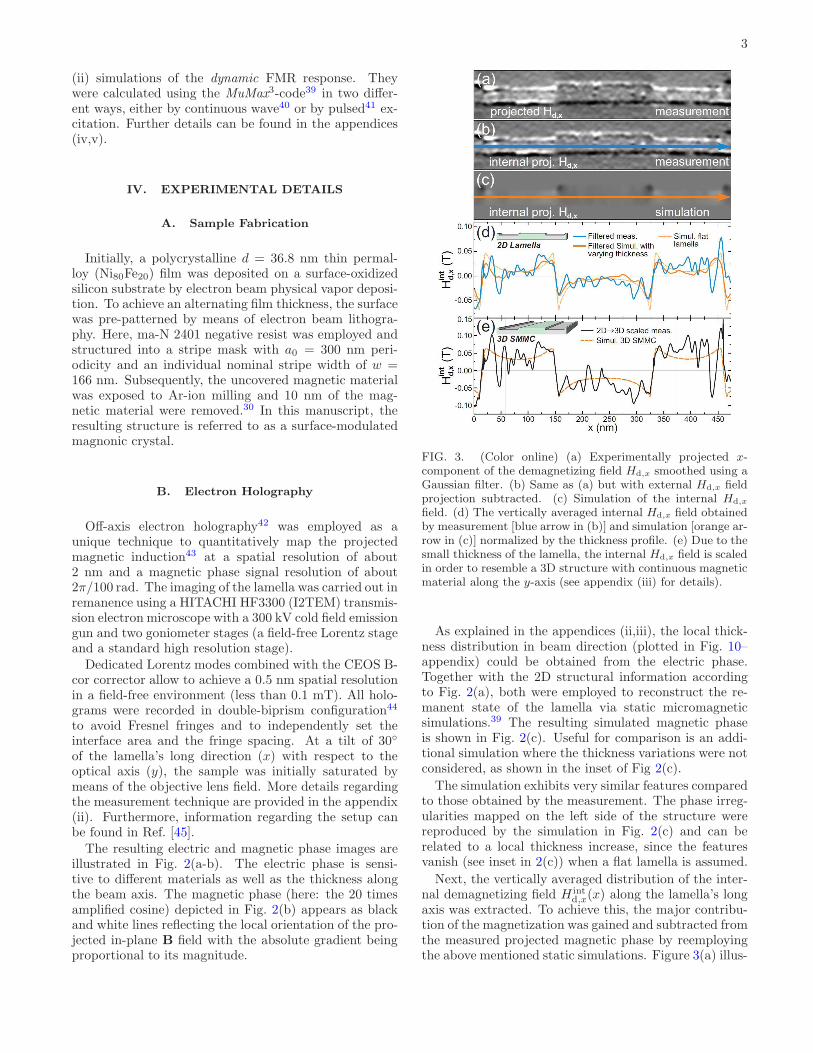
FIG. 3. (Color online) (a) Experimentally projected x-component of the demagnetizing field Hd,x smoothed using aGaussian filter. (b) Same as (a) but with external Hd,x fieldprojection subtracted. (c) Simulation of the internal Hd,x
field. (d) The vertically averaged internal Hd,x field obtainedby measurement [blue arrow in (b)] and simulation [orange ar-row in (c)] normalized by the thickness profile. (e) Due to thesmall thickness of the lamella, the internal Hd,x field is scaledin order to resemble a 3D structure with continuous magneticmaterial along the y-axis (see appendix (iii) for details).
As explained in the appendices (ii,iii), the local thick-ness distribution in beam direction (plotted in Fig. 10–appendix) could be obtained from the electric phase.Together with the 2D structural information accordingto Fig. 2(a), both were employed to reconstruct the re-manent state of the lamella via static micromagneticsimulations.39 The resulting simulated magnetic phaseis shown in Fig. 2(c). Useful for comparison is an addi-tional simulation where the thickness variations were notconsidered, as shown in the inset of Fig 2(c).
The simulation exhibits very similar features comparedto those obtained by the measurement. The phase irreg-ularities mapped on the left side of the structure werereproduced by the simulation in Fig. 2(c) and can berelated to a local thickness increase, since the featuresvanish (see inset in 2(c)) when a flat lamella is assumed.
Next, the vertically averaged distribution of the inter-nal demagnetizing field H int
d,x(x) along the lamella’s longaxis was extracted. To achieve this, the major contribu-tion of the magnetization was gained and subtracted fromthe measured projected magnetic phase by reemployingthe above mentioned static simulations. Figure 3(a) illus-

4
FIG. 4. (Color online) f(H0) dependences of the surface-modulated magnonic crystal with the gray scale representing thedynamic response. (a) Measurement and (b-d) different simulations of the FMR response. (b) Simulation based on thestructural shape of the magnonic crystal. In (c-d) the internal demagnetizing field H int
d,x was added to a 36 nm thin film with
subsequent calculation of the FMR response. (c) is based on the measured H intd,x field and (d) on the simulated one.
trates the resulting 2D distribution of the magnetic phasegenerated by the Hd,x field with white (black) color rep-resenting a positive (negative) sign of Hd,x. This meansthat Hd,x is acting as demagnetizing ormagnetizing field,respectively. Figure 3(b) only depicts the projected in-ternal Hd,x field isolated by subtraction of the contrastgenerated by the simulated stray field outside the mag-netic structure. Hence, the stray field features above theSMMC in Fig. 3(a) vanish in 3(b). Moreover, there areparasitic contribution to the projected internal field dueto the external strayfield in the front and in the backof the lamella with respect to the beam direction. Suchcontributions were also estimated using the static micro-magnetic simulations.
In Fig. 3(d) the vertically averaged profiles of H intd,x
are presented according to the arrows in Figs. 3(b-c).The values taken from Figs. 3(b-c) are normalized bythe lamella thickness profile discussed in the appendix(iii). Blue color represents the measurement and or-ange color the simulation. The profiles demonstrate avery good agreement between both the measurement andthe simulation and are corroborated with the simulatedH int
d,x(x)-distribution of a flat structure (orange dashed
line), where the lamella thickness was fixed to tavg.
Since further investigations focus on a 3D extendedMC and not on a thin (2D) lamella structure, system-atic difference between the internal fields of both systemsneed to be considered. As further described in the ap-pendix (iii), this circumstance is addressed by a scalingof H int
d,x(x) with the result shown as black solid line in
Fig. 3(e). Apart from the apparent oscillations arisingfrom measurement noise, the result matches well the dis-tribution obtained by the simulation (orange dashed linein Fig. 3(e)) of an ideal 3D SMMC.
C. Magnetic Characterization
The magnetic characterization was carried out using abroadband vector network analyzer ferromagnetic reso-nance (FMR) setup as described in Refs. [30,46]. Exci-
tation of the spin system is achieved by coupling a mi-crowave signal via a coplanar waveguide to the surfaceof a ‘flip-chip’-mounted sample. The transmission signalS21 is measured at several fixed excitation frequencies fsweeping the external field H0. The absolute value of S21
was recorded as the FMR-response.
V. RESULTS AND DISCUSSION
In this section, the results from two independent ap-proaches to reconstruct the effective spin-dynamics in amagnonic crystal are discussed. With both the knowl-edge of (i) the structural shape and (ii) the internal Hd,x
field, dynamic simulations were performed.
A. Frequency dependence in backward-volume
geometry
Figure. 4 illustrates several f(H0) dependences ob-tained from measurement and simulations. In 4(a) themeasured f(H0) is shown whereas 4(b) was obtainedfrom the remodeling of the sample structure and sub-sequent FMR simulations. The evident similarity be-tween both indicates a reliable representation of the sam-ple structure by the micromagnetic model. In contrast,Fig. 4(c) and (d) are obtained by simulating a 36 nm thinpermalloy film with a virtually added periodic distribu-tion of H int
d,x. In 4(c) the measured field distribution was
employed and in 4(d) the simulated one was taken corre-sponding both to the two plots in Fig. 3(e). A convincingqualitative agreement of all shown f(H0) dependenceswith the measurement is obtained.However, at second glance, a higher number of modes
can be found in Fig. 4(c), which is due to the measure-ment noise in H int
d,x violating the mirror symmetry of theinternal field landscape. Especially at the edges of thethick part, the different local demagnetizing fields leadto the occurrence of two separate non-symmetric edgemodes with different energies. However, for the symmet-ric H int
d field in Fig. 3(d), the f(H0) matches well the one

5
obtained in Fig. 3(b) with similar mode characteristics.
B. Mode profiles
Another way to test the level of similarity between thedifferent simulations presented above is to analyze themode profiles. In Fig. 5 the profiles of the resonant spinwaves at f = 12 GHz are plotted and labeled with therespective mode number n. The plots indicate a con-vincing agreement between both simulations such thatthe individual character of the plotted mode profiles re-flects similar physics. Consequently, the dynamics of theSMMC is very similar to flat MC with a pronounced in-ternal field structure, such as bi-component MCs. Thedynamics of such systems can be well described by theplane wave method,7,36–38 which was used in additionfor the calculation of the mode profiles in Fig. 5 con-firming the results from the simulations. Note that thefrequency of 12 GHz was selected such that effects frommode coupling are small and, thus, can be neglected inthe following discussion.The reason for the multitude of measurable spin-wave
modes in SMMCs is explained by Fig. 6(a). Here, thef(H0) dependence of the modes in the limit of a thinfilm with tiny modulation ∆d → 0 is plotted. Apartfrom the uniform mode, standing spin-wave modes arepresent, with a defined number of nodes (2n) fitting inone period a0 as sketched in the inset of Fig. 6(a). Thiscircumstance results in a quantization of the wave vectorwith k = 2πn/a0. By applying Eqs. (1)–(3), the cor-responding frequency dependence can be obtained (or-ange lines). The standing spin-wave modes can couple tothe uniform mode and together form the full spectrumof possible states accessible in such structures.30,32,33 InFig. 6(a), at the marked frequency of 12 GHz, three stateswith lower energy than the uniform one with n = 1, 2, 3are found and with the n = 2 state being lowest. Notethat for a given frequency, the mode energy is reflected bythe resonance field such that for low (high) energy modesa high (low) external field must be supplied to resonate atthe same frequency. Thus, at f = const., high resonancefields represent low mode energy and reverse.For an SMMC with a pronounced modulation, these
states are present as well, but are shaped differently bythe internal field landscape. In Fig. 5, all modes can stillbe identified according to their total number of nodes(2n) inside a period a0. However, due to the presenceof the internal field landscape, the modes can no longerbe described assuming a constant wave vector due tok = 2πn/a0 and an extension over the full MC. Instead,the modes 0–3 reveal a clear localization in either thethick or the thin part and all modes show major devia-tions from the harmonic character sketched in the insetof Fig. 6(a), which can only be explained with the helpof the internal field landscape shown in Fig. 6(b). Thefield distribution (orange) is translated into a region map(roman numbers) of negative (I,II) and positive (III,IV)
-1.0
-0.5
0.0
0.5
1.0
4
0
1
2
3
Simulation Film withinternal H -Fieldd,x
Simulation Structure
Theory PWM
Norm
.A
mplit
ude
-1.0
-0.5
0.0
0.5
1.0
-1.0
-0.5
0.0
0.5
1.0
0 50 100 150 200 250 300
x (nm)
50 100 150 200 250 300
x (nm)
93mT
129mT
170mT
202mT
235mT
n=4
n=0
n=3
n=1
n=2
FIG. 5. (Color online) Mode profiles of spin-waves (with cor-responding mode number n) at different resonance positionsas marked in Figs. 4 and 8. They are derived by simulationsand PWM theory.
internal fields. The dashed lines represent the part ofthe field landscape where the respective mode energy issufficient for a spin-wave excitation.In order to understand the characteristic mode pro-
files in Fig. 5, it is useful to know the dependence of thewave vector k on the effective field Hn
eff = Hn0 + H int
d .At this point, the knowledge of the internal demagnetiz-ing field H int
d becomes relevant again. As the H intd field
itself depends on the location along the x-axis, the dis-tribution H int
d (x) can be used to assign a specific k-valuewith a location inside the MC. Moreover, this relationcan be used to identify regions where no k-value can beattributed to the effective field which is important forunderstanding the individual mode localization. For thispurpose, the spin-wave dispersion expressed by Eqs. (1)–(3) is employed with H0 being replaced by the effectivefield Hn
eff = Hn0 + H int
d to consider both, the externalfield of the nth spin wave in resonance Hn
0 as well as theinternal demagnetizing field H int
d . Accordingly, the de-pendence of the effective field Hn
eff on the wave vector kreads (for ϕk = 0◦):
µ0Hneff =− 1
2µ0MSF+
[
14 (µ0MSF )
2+
(
ω
γ
)2 ]12
(4)
Eq. (4) can now be used, to correlate the wave vector withthe effective field at f = 12 GHz, which is illustrated inFig. 7(a) for both the thick and the thin part of the MC.With the given resonance fields in Fig. 5 and the knowl-edge of the internal demagnetizing field H int
d (x), the ef-fective fields can be calculated for all different locationsin the SMMC and for each spin-wave mode. The coloredlines in Fig. 7(a) correspond to the range of k-values as-sociated with the internal field landscape for each mode.Bright colors represent the edge regions (I,IV) and darkcolors represent the center regions (II,III). In Fig. 7(b),the H int
d (x) distribution (orange dashed line in Fig. 3(e))

6
0.0 0.1 0.2 0.3 0.4 0.5
Field (T)
n=4
n=3
n=2
n=1
standing spin waves
0
15
20
f (G
Hz)
25
n=1n=2
10
Film limit
uniform
(n=0) II I IIIIII IIIIV IV IV IV
4
0
Inte
rnal d
em
ag.field
(a) (b)
1
Location
2
f = 12 GHz
3
FIG. 6. (Color online) (a) f(H0) in the film limit with tinymodulation. Standing spin-waves modes appear quantizeddue to k = 2πn/a0 and are sketched in the inset. (b) Modelocalization and internal field landscape of an SMMC. TheH int
d field is negative in region I and II and positive in regionIII and IV. Thus, modes with energy below the uniform mode(flat black line) can only be excited in the regions where theinternal field is reduced (I,II).
is used, to calculate the wave vector dependent on thelocation along the x-axis.With Fig. 7(a) and (b), the reason for the mode local-
ization can be explained. For modes 1–3, the effectivefield in the thin part (III,IV) exceeds 176 mT, which ismaximum value (vertex of the gray parabola in 7(a)) fora defined spin-wave excitation in this region. Thus, allthree modes localize in the thick part (I,II) and avoid theregions III and IV. Moreover, the calculations reveal thatmode 2 is only excited at the edges of the thick part (I).It is important to note that in SMMCs with a pro-
nounced modulation, a classical uniform mode cannotexist due to the variance of the internal fields. Instead,mode 0 behaves as a quasi-uniform excitation of the cen-ter of the thin part (III,IV) of the MC, which is supportedby the mode profile in Fig. 5 and by the range of k-valuesin Fig. 7(b) reaching almost perfectly k = 0 in the centerof part III. Unlike the higher modes 2–4, the wave vectorof mode 0 and mode 1 is not only delimited by the verticesof the parabolae in Fig. 7(a) where the energy becomestoo small for a spin-wave excitation. It is also delim-ited by the uniform state (k = 0) at µ0Heff = 154 mTsuch that regions of lower internal fields cannot be ex-cited anymore. Due to that reason, mode 0 avoids thethick part (I,II) as much as mode 1 avoids region I asshown in Fig. 7(b) and confirmed by Fig. 5.The only mode with sufficient energy to spread over
the full MC is mode 4. In Fig. 7(a) and (b) the dis-tribution of the modes’ wave vector is plotted accord-ing to Eq. (4). Expressed vividly, the mode can re-arrange its 8 nodes in a way that the energy of themode is distributed equally over the full structure. Thenumber of nodes in the thick part m and in the thinpart l can be estimated by solving µ0H
thick0 = µ0H
thin0 ,
i.e. µ0Hm0
(
d = 36 nm, µ0Hthickd = −39mT, k = mπ
w
)
=
µ0Hl0
(
d = 26 nm, µ0Hthind = 41mT, k = lπ
a0−w
)
with n = m + l and with Hthickd and Hthin
d being theaverage internal demagnetizing fields of the thick and the
0 50 100 150 2000.00
0.02
0.04
0.06
0.08
0.10
0.12
thin
thick
4
4
0
0 100 200 300
x (nm)
(a) (b)II I IIIIII IIIIV IV IV IV
Effective Field (mT)
Wa
ve
ve
cto
r (n
m)
-1
1
2
3 4
3
02
1
FIG. 7. (Color online) wave vector calculation for the reso-nances marked in Fig. 5 dependent on (a) the effective fieldand (b) the location along the x-axis. For modes 1–3, theinternal fields in the thin part are so high that the effectivefield exceeds the vertex of the parabola in (a) and thus, thisregion is avoided. In (a) bright lines correspond to the edge(I,IV) and dark lines correspond to the center regions (II,III).
thin part of the MC. Applying Eq. (4) yields a resonancefield of µ0H
m0 = µ0H
l0 = 103 mT and the node numbers
m = 5.29 and l = 2.71, which is coherent with the nodedistribution in Fig. 5.In short, it is observed, that three kinds of modes are
distinguished in the SMMC. (i) A quasi-uniform centralexcitation of the thin part of the SMMC, which corre-sponds to mode 0. (ii) k 6= 0 modes with sufficient energyto extend over the full MC (e.g. mode 4) and (iii) k 6= 0modes with insufficient energy enforcing a localization inthe thick part (I,II) of the MC, such as mode 1–3.Modes of category (ii) adapt their wave vector such
that the mode energy is equally distributed over the fullstructure while the total number of nodes (2n = m + l)is conserved. For these modes, the wave vector mustbe calculated separately for both the thick and the thinpart as explained above. This is different for the category(iii) of localized modes. These modes exhibit a ‘damped’trough in the thin part where the local fields are too highfor a spin-wave excitation. The residual 2n− 1 nodes ofthe modes are condensed in the thick part, where theinternal field is reduced. Accordingly, the wave vectorof these modes is shifted to k = (2n − 1)π/w instead of2πn/a0 in the thin film limit.
C. Angular Dependence
Figure 8(a) shows the measurement and 8(b) the sim-ulation of the angular dependence at f = 12 GHz. Thebackward-volume direction (ϕH = 0◦, 180◦) is markedby the orange line with the labeled resonances being thesame as in Fig. 4(b). ϕH = 90◦ and 270◦ both corre-spond to the Damon-Eshbach geometry. Again, a satis-factory reconstruction of the measurement by the simu-lation based on the sample structure is obtained.The most prominent resonance branch is the flat one
between 45◦–135◦ and 225◦–315◦. This mode corre-sponds to the uniform mode around the Damon-Eshbach

7
geometry with negligible internal demagnetizing fields.In the same angular range, there is a second less no-ticeable resonance branch observed at lower externalfields corresponding to the n = 1 Damon-Eshbach mode.Knowing that the n = 1 mode is identified at µ0H0 =202 mT in the backward-volume direction, mode 1 canbe followed through a full 360◦ rotation of the externalfield.In order to analytically express the angular dependence
of a mode, Eqs. (1)–(3) can again be employed togetherwith the identity ϕk = ϕH . Around the backward-volume direction, the high internal demagnetizing fieldsmust also be taken into account with regard to the indi-vidual mode localization. In order to include the demag-netizing field into the angle-dependent spin-wave disper-sion, µ0H0 was replaced by µ0H0 + µ0Hd · cos (2ϕH) inEq. (2) and by µ0H0 + µ0Hd · cos2ϕH in Eq. (3) analo-gous to the description of a uniaxial anisotropy field.46–48
From Eqs. (1)–(3), a modified angular dependence is ob-tained
µ0Hn0 (ϕH) = − 1
2µ0Hd
(
cos(2ϕH)+cos2ϕH)
−Dk2
− 12µ0MSF− 1
2µ0MS(1−F ) sin2ϕH+
[
14µ
20H
2d sin
4ϕH
+ 12µ
20HdMSF sin2ϕH− 1
2µ20HdMS(1−F ) sin4ϕH
+ 14
(
µ0MSF−µ0MS(1−F ) sin2ϕH)2+
(
ω
γ
)2 ]12
(5)
with µ0Hn0 the resonance field of the nth mode. The
angle-dependent resonance fields are calculated usingEq. (5) employing simplified assumptions: (i) The wavevector of localized k 6= 0 modes is defined by k =(2n− 1)π/w and (ii) for the effective demagnetizing fieldHeff
d the average value of the regions in which the modeslocalizes is taken. (iii) As explained in Sec. VB, formodes localized in the thick as well as the thin part ofthe MC (e.g. mode 4), the node number and the effectivefield Heff
d are calculated separately for both parts.The calculated angle dependences according to Eq. (5)
are depicted in Fig. 8 as solid lines revealing a firm over-all agreement to the measurement and the simulation.The parameters used for the calculations according tothe above assumptions are provided in table I. Mode 3 isthe only one with major deviations from the resonancepositions in the colorplot. The discrepancy is likely duea different pinning condition at the edge of the thickpart resulting in an overestimation of the wave vector byk = (2n− 1)π/w. This is supported by the mode profilein Fig. 5 revealing a reduced wave vector between the filmlimit 2πn/a0 and (2n−1)π/w. A fitting angle-dependentresonance position can be obtained for k = 4.3π/w (bluedot-dashed line in Fig. 8(b)), which is coherent with thenumber of nodes in Fig. 5.For the calculations in and around the Damon-Eshbach
geometry, the internal demagnetizing fields were ne-glected, i.e. , µ0H
effd = 0. Interestingly, a reliable re-
production of the behavior of mode 1 (dark blue line in
Fie
ld (
mT
)
0° 45° 90° 135° 180° 225° 270° 315° 360°0
50
100
150
200
In-plane angle jH
Fie
ld (
mT
)
0
50
100
150
200
250
measurement
simulation
4
0
2
3
250
H HH
1
(a)
(b) calc. basedon Eq. (4)
FIG. 8. (Color online) In-plane angular dependence of theresonance fields of an SMMC with 10 nm modulation height,where (a) is the measurement and (b) the corresponding sim-ulation. The numbered resonances correspond to the modeprofiles shown in Figs. 5. The solid lines are calculationsbased on Eq. (5) with parameters accounting for ϕH = 135◦–225◦ provided in table I. For ϕH = 225◦–270◦, mode 1 wasdescribed without consideration of an internal demagnetizingfield assuming a film thickness of d = 26 nm.
Fig. 8(b)) can only be obtained if a dynamically activefilm thickness of only d = 26 nm (corresponding to thethin part) is assumed.
VI. CONCLUSION
Electron holography measurements were employed tomap the internal magnetic field landscape of a surfacemodulated magnonic crystal on the nanoscale. The mea-surements confirmed the alternating character of the de-magnetizing field acting locally as demagnetizing- and
TABLE I. Parameters used for the calculation angular depen-dence of the spin waves between ϕH = 135◦–225◦.
mode no. n localisation d (nm) keff µ0Heffd (mT)
0 III 26 0 31.9
1 II 36 π/w -31.8
2 I 36 3π/w -57.0
3 I,II 36 5π/w -38.7
4 I–IV26 2.71π
a0−w-38.7
36 5.29π/w 40.9

8
magnetizing field. Micromagnetic reconstructions of itsdynamic behavior revealed the dominating role of themagnonic crystals’ internal demagnetizing field. The sig-nificant impact of the internal field landscape on themode profiles and the modes’ angular dependences werediscussed.
VII. ACKNOWLEDGMENT
We thank B. Scheumann for the film deposition, A.Kunz for the FIB lamella preparation and Y. Yuan andS. Zhou for the VSM characterization as well as H. Lichtefor fruitful discussions. Support by the NanofabricationFacilities Rossendorf at IBC as well as the infrastruc-ture provided by the HZDR Department of InformationServices and Computing are gratefully acknowledged.Our research has received funding from the GraduateAcademy of the TU Dresden, from the European UnionSeventh Framework Program under grant no. 312483-ESTEEM2 (Integrated Infrastructure Initiative-I3), theCenters of Excellence with Basal/CONICYT financ-ing (grant no. FB0807), CONICYT PAI/ACADEMIA79140033, FONDECYT 1161403, CONICYT PCCI(grant no. 140051) and DAAD PPP ALECHILE (grantno. 57136331) and from the Deutsche Forschungsgemein-schaft (grant no. LE2443/5-1).
VIII. APPENDIX
This section contains details regarding (i) the fabri-cation of the TEM lamella, (ii) the electron holographytechnique, (iii) the extraction of the internal demagne-tizing field and (iv) the static and (v) the dynamic sim-ulations carried out in this work.
(i) Lamella Fabrication The cross-sectional TEMlamella of the magnonic crystal was prepared by in-situ lift-out using a Zeiss Crossbeam NVision 40 system.In order to protect the structure surface, a carbon caplayer was deposited by electron beam assisted precur-sor decomposition and subsequent Ga focused ion beam(FIB) assisted precursor decomposition. Subsequently,the TEM lamella was prepared using a 30 keV Ga FIBwith adapted currents. Its transfer to a 3-post copperlift-out grid (Omniprobe) was done with a Kleindiek mi-cromanipulator. To minimize sidewall damage, Ga ionswith 5 keV energy were used for final thinning of theTEM lamella until electron transparency was achieved.
(ii) Off-Axis Electron Holography Figure 9(a)illustrates the working principle of an off-axis electronholography setup. Employing a Mollenstedt biprism, theobject- and the reference beam is precisely superimposedat the image plane. The recorded interference fringe pat-tern is shown in Fig. 9(b) with tiny contrast variationsand fringe bending (see inset in Fig. 9(b)). The holo-
FIG. 9. (Color online) Acquisition and reconstruction schemeof an electron hologram. (a) Setup of electron holography inTEM. (b) Hologram of a permalloy (Ni80Fe20) thin film with∆d = 10 nm surface modulation. (c) Fourier spectrum of thehologram showing two sidebands and one center band. TheFourier transform of the upper sideband, low-pass filtered bya numerical aperture, yields the image wave represented by(d) the (wrapped) amplitude and (e) the phase image.
gram is reconstructed by employing the upper sidebandof the hologram’s Fourier spectrum (see Fig. 9(c)). Byinverse Fourier transformation the amplitude and phaseinformation depicted in Fig. 9(d) and Fig. 9(e) are ob-tained. The phase unwrapping is carried out using theGoldstein algorithm.49 The hologram series acquisition(40 holograms for each orientation) and the wave aver-aging were employed to reduce the phase noise.50 Notethat displacement removal and first-order aberration cor-rections were required to match the mean phase.The electron phase is sensitively altered by electric and
magnetic properties of the sample and is, thus, key quan-tity for the field mapping on the nanoscale34 given by
ϕ(x, z) = CE
tu(x,z)∫
tl(x,z)
V (x, y, z)dy −e
~
∫∫
S
BdA . (6)
The first integral is the projection of the electrostatic po-tential V along the beam (y-)direction constricted by thelocal lamella thickness t(x, z) = tu − tl. The interactionconstant CE is about 0.0065 (Vnm)−1 at 300 kV. Beingproportional to the magnetic flux of a magnetic induc-tion B = µ0Hd+µ0M through the surface S enclosed bythe object- and the reference beam, the second integralquantifies the magnetic contribution to the phase.

9
Flipping the sample upside down51 for a second mea-surement yields ϕflipped, which can be used to separatethe electric ϕel and magnetic phase shift ϕmag as shownin Fig. 2(a-b):
ϕel =1
2(ϕ+ ϕflipped) (7)
ϕmag =1
2(ϕ− ϕflipped) (8)
As evident from Eq. (6), the electric phase contains thefull information about the 3D sample geometry, whichwas further used to rebuild the structure for micromag-netic simulations. As another implication, the gradient ofthe magnetic phase returns purely the projected in-planecomponents of the magnetic induction:
∇ϕmag(x, z) =e
~
+∞∫
−∞
B×dy
=µ0e
~
tu(x,z)∫
tl(x,z)
(M+Hintd )×dy+
∞∫
tu(x,z)
Hextd ×dy+
tl(x,z)∫
−∞
Hextd ×dy
(9)
To obtain the internal demagnetizing field Hintd , a de-
composition of B into the magnetization M and the de-magnetizing field Hd is necessary. A deeper technicaldescription of the acquisition of a TEM hologram is pro-vided in Refs. [42 and 50].
(iii) Internal Demagnetizing Field ExtractionAfter removing the phase contributions of the externalstrayfield (see Sec. IVB), the vertically averaged distribu-tion of the internal Hd,x field was obtained by employinga numerical mask inside the magnetic region. In order toreduce the number of artifacts, areas of large phase noisewere neglected. To achieve absolute field values in Tesla,the integrated magnetic phase was divided by the locallamella thickness (shown in Fig. 10). Here, the field wasaveraged with the length of the vertical integration pathand a Gaussian filter was applied in order to improve thesignal-to-noise ratio of the extracted field distribution inFig. 3(d).To reconstruct the H int
d,x(x)-distribution of an extended
SMMC, a field scaling was necessary (see Sec. IVB) dueto two reasons. First, systematic deviations between thethickness-varied and Gaussian filtered simulation (solidorange line in Fig. 3(d)) and the simulation of a perfectlyflat lamella (dashed orange line in Fig. 3(d)) were quan-tified and corrected. Second, the systematic differencesof the internal field in a flat (tavg = 38.3 nm thick) 2Dstructure compared to the field in a 3D magnonic crys-tal needed to be regarded. Therefore, a scaling functionwas defined based on the static simulation of a flat quasi2D lamella (dashed orange line in Fig. 3(d)) and a 3DSMMC (dashed orange line in Fig. 3(e)). Since the fieldvalues differ by more than one order of magnitude, the
FIG. 10. (Color online) Local lamella thickness t in beamdirection determined from the electric phase depicted inFig. 2(a).
scaling was performed logarithmically:
H3Dd,x(x) =
H2Dd,x(x)
∣
∣
∣H2Dd,x(x)
∣
∣
∣
·∣
∣H2Dd,x(x)
∣
∣
(
log |H3D,simd,x
(x)|log |H2D,sim
d,x(x)|
)
(10)
Here, H3Dd,x(x) denotes the resulting 3D-corrected field
measurement and H2Dd,x(x) is the measured distribution
of the thin (2D) lamella. The same field distribu-
tions obtained by simulations are labeled H3D,simd,x (x) and
H2D,simd,x (x), respectively. Note that the index ‘int’ was
omitted in Eq. (10).
(iv) Static Simulations For a thorough reconstruc-tion of the lamella structure, static simulations werecarried out. First, the average thickness tavg of a flatlamella was varied until the magnetic phase inside theMC matched the mean phase obtained by measurement.With the help of that, the variations of the electric phase(Fig. 2(a)) inside the MC could be translated into localthickness variations with the result shown in Fig. 10. Inorder to consider tiny thickness variations in the staticsimulations, the saturation magnetization was scaled lo-cally by M
′
S(x, y) = t(x, y)/tavg · MS with a cell sizeof 2.438 nm · 2.125 nm · 2.410 nm for a high resolution.Note that the thickness along the beam axis was fixed tothe average value of tavg = 38.3 nm. MS = 735 kA/m,D = 23.6 Tnm2 and the g-factor g = 2.11 were selectedaccording to the material parameters of a permalloy ref-erence film.30
In order to compare a perfect (flat) 2D lamella witha 3D SMMC, the micromagnetic model above was mod-ified omitting the local scaling of MS with and withoutperiodic boundary conditions in y-direction.
(v) Dynamic Response Simulations The dy-namic response simulations39 were performed in two dif-ferent ways. In order to obtain frequency-field depen-dencies (see Fig. 4), pulsed41 simulations were calcu-lated. To simulate the angle-dependent spin-wave res-onance (shown in Fig. 8), a continuous-wave approach40
was chosen. As the latter does not require Fourier-transformations in frequency-space, such simulationscould directly be carried out at f = 12 GHz.

10
Two different simulation geometries were selected: (i)a structural reconstruction of the shape of the magnoniccrystal and (ii) an approach using the internal demagne-tizing field H int
d,x(x) only as an additive field in a 36 nmthin permalloy film.For the structural reconstruction of the magnonic crys-
tal, the micromagnetic model according to the electricalphase image of the magnonic crystal (Fig. 2(a)) was ap-plied. Minor changes of the simulation layout accord-ing to different average values of a0 = 300 nm andw = 166 nm were regarded and, furthermore, the ge-ometry was symmetrized. The modulation height wasfixed to the value of ∆d = 10 nm with a continuous film
of 26 nm thickness underneath. For an appropriate cross-sectional resolution, a cell size of 2.344 nm · 4 nm · 2 nmwas chosen with 128 · 16 · 18 cells in total. In order torealize a continuous elongation of the structure, the ge-ometry was repeated 30 times in the x- and 100 times inthe y-direction.In the second approach, the internal demagnetizing
field H intd,x(x) of the MC was added to an unmodulated
continuous thin film. Due to the symmetry in z-direction,a larger cell-size of 12 nm was chosen with 3 cells in to-tal along the z-axis. The cell size and the cell numberalong the x- and y-axis as well as the 2D repetitions wereselected equivalently.
1 V. V. Kruglyak, S. O. Demokritov, and D. Grundler, J.Phys. D: Appl. Phys. 43, 264001 (2010).
2 G. Gubbiotti, S. Tacchi, M. Madami, G. Carlotti, A. O.Adeyeye, and M. Kostylev, J. Phys. D: Appl. Phys. 43,264003 (2010).
3 B. Lenk, H. Ulrichs, F. Garbs, and M. Munzenberg, Phys.Rep. 507, 107 (2011).
4 M. Krawczyk and D. Grundler, J. Phys. Condens. Matter26, 123202 (2014).
5 A. V. Chumak, V. I. Vasyuchka, A. A. Serga, and B. Hille-brands, Nat. Phys. 11, 453 (2015).
6 S. Tacchi, G. Duerr, J. W. K los, M. Madami, S. Neusser,G. Gubbiotti, G. Carlotti, M. Krawczyk, and D. Grundler,Phys. Rev. Lett. 109, 137202 (2012).
7 M. Krawczyk, S. Mamica, M. Mruczkiewicz, J. W. K los,S. Tacchi, M. Madami, G. Gubbiotti, G. Duerr, andD. Grundler, J. Phys. D: Appl. Phys. 46, 495003 (2013).
8 F. Montoncello, S. Tacchi, L. Giovannini, M. Madami,G. Gubbiotti, G. Carlotti, E. Sirotkin, E. Ahmad, F. Y.Ogrin, and V. V. Kruglyak, Appl. Phys. Lett. 102, 202411(2013).
9 M. Kostylev, P. Schrader, R. L. Stamps, G. Gubbiotti,G. Carlotti, A. O. Adeyeye, S. Goolaup, and N. Singh,Appl. Phys. Lett. 92, 132504 (2008).
10 K.-S. Lee, D.-S. Han, and S.-K. Kim, Phys. Rev. Lett.102, 127202 (2009).
11 Z. K. Wang, V. L. Zhang, H. S. Lim, S. C. Ng, M. H. Kuok,S. Jain, and A. O. Adeyeye, Appl. Phys. Lett. 94, 083112(2009).
12 Z. K. Wang, V. L. Zhang, H. S. Lim, S. C. Ng, M. H. Kuok,S. Jain, and A. O. Adeyeye, ACS Nano 4, 643 (2010).
13 F. S. Ma, H. S. Lim, V. L. Zhang, S. C. Ng, and M. H.Kuok, Nanoscale Res. Lett. 7, 1 (2012).
14 D. Kumar, J. W. K los, M. Krawczyk, and A. Barman, J.Appl. Phys. 115, 043917 (2014).
15 A. V. Chumak, V. S. Tiberkevich, A. D. Karenowska, A. A.Serga, J. F. Gregg, A. N. Slavin, and B. Hillebrands, Nat.Commun. 1, 141 (2010).
16 M. Vogel, A. V. Chumak, E. H. Waller, T. Langner, V. I.Vasyuchka, B. Hillebrands, and G. von Freymann, Nat.Phys. 11, 487 (2015).
17 J. Topp, D. Heitmann, M. P. Kostylev, and D. Grundler,Phys. Rev. Lett. 104, 207205 (2010).
18 S. Tacchi, M. Madami, G. Gubbiotti, G. Carlotti,S. Goolaup, A. O. Adeyeye, N. Singh, and M. P. Kostylev,
Phys. Rev. B 82, 184408 (2010).19 J. Topp, S. Mendach, D. Heitmann, M. Kostylev, and
D. Grundler, Phys. Rev. B 84, 214413 (2011).20 J. Ding, M. Kostylev, and A. O. Adeyeye, Phys. Rev. Lett.
107, 047205 (2011).21 C. S. Lin, H. S. Lim, V. L. Zhang, Z. K. Wang, S. C. Ng,
M. H. Kuok, M. G. Cottam, S. Jain, and A. O. Adeyeye,Journal of Applied Physics 111, 033920 (2012).
22 K. Di, S. X. Feng, S. N. Piramanayagam, V. L. Zhang,H. S. Lim, S. C. Ng, and M. H. Kuok, Sci. Rep. 5, 10153(2015).
23 H. Yu, G. Duerr, R. Huber, M. Bahr, T. Schwarze,F. Brandl, and D. Grundler, Nat. Commun. 4, 2702(2013).
24 M. P. Kostylev, A. A. Serga, T. Schneider, B. Leven, andB. Hillebrands, Appl. Phys. Lett. 87, 153501 (2005).
25 K.-S. Lee and S.-K. Kim, J. Phys. D: Appl. Phys. 104,053909 (2008).
26 A. Khitun, M. Bao, and K. L. Wang, J. Phys. D: Appl.Phys. 43, 264005 (2010).
27 K. Vogt, F. Fradin, J. Pearson, T. Sebastian, S. Bader,B. Hillebrands, A. Hoffmann, and H. Schultheiss, Nat.Commun. 5, 3727 (2014).
28 S.-K. Kim, K.-S. Lee, and D.-S. Han, Appl. Phys. Lett.95, 082507 (2009).
29 M. Inoue, A. Baryshev, H. Takagi, P. B. Lim, K. Hata-fuku, J. Noda, and K. Togo, Appl. Phys. Lett. 98, 132511(2011).
30 M. Langer, K. Wagner, T. Sebastian, R. Hubner, J. Gren-zer, Y. Wang, T. Kubota, T. Schneider, S. Stienen,K. Lenz, H. Schultheiss, J. Lindner, K. Takanashi, R. E.Arias, and J. Fassbender, Appl. Phys. Lett. 108, 102402(2016).
31 I. Barsukov, F. M. Romer, R. Meckenstock, K. Lenz,J. Lindner, S. Hemken to Krax, A. Banholzer, M. Korner,J. Grebing, J. Fassbender, and M. Farle, Phys. Rev. B 84,140410 (2011).
32 P. Landeros and D. L. Mills, Phys. Rev. B 85, 054424(2012).
33 R. A. Gallardo, A. Banholzer, K. Wagner, M. Korner,K. Lenz, M. Farle, J. Lindner, J. Fassbender, and P. Lan-deros, New J. Phys. 16, 023015 (2014).
34 H. Lichte, Ultramicroscopy 108, 256 (2008).35 B. A. Kalinikos and A. N. Slavin, J. Phys. C 19, 7013
(1986).

11
36 M. L. Sokolovskyy and M. Krawczyk, J. Nanopart. Res.13, 6085 (2011).
37 J. W. K los, D. Kumar, J. Romero-Vivas, H. Fangohr,M. Franchin, M. Krawczyk, and A. Barman, Phys. Rev.B 86, 184433 (2012).
38 R. A. Gallardo, M. Langer, A. Roldan-Molina, T. Schnei-der, K. Lenz, J. Lindner, and P. Landeros, ArXiv:1610.04176 (2016).
39 A. Vansteenkiste, J. Leliaert, M. Dvornik, M. Helsen,F. Garcia-Sanchez, and B. Van Waeyenberge, AIP Adv.4, 107133 (2014).
40 K. Wagner, S. Stienen, and M. Farle, ArXiv: 1506.05292(2015).
41 R. D. McMichael and M. D. Stiles, J. Appl. Phys. 97,10J901 (2005).
42 M. Lehmann and H. Lichte, Microscopy and Microanalysis8, 447 (2002).
43 M. Korner, F. Roder, K. Lenz, M. Fritzsche, J. Lindner,H. Lichte, and J. Fassbender, Small 10, 5161 (2014).
44 K. Harada, A. Tonomura, Y. Togawa, T. Akashi, andT. Matsuda, Applied Physics Letters 84, 3229 (2004).
45 E. Snoeck, F. Houdellier, Y. Taniguch, A. Masseboeuf,C. Gatel, J. Nicolai, and M. Hytch, Microscopy and Mi-croanalysis 20, 932 (2014).
46 M. Korner, K. Lenz, R. A. Gallardo, M. Fritzsche,A. Mucklich, S. Facsko, J. Lindner, P. Landeros, andJ. Fassbender, Phys. Rev. B 88, 054405 (2013).
47 K. Lenz, E. Kosubek, K. Baberschke, H. Wende, J. Her-fort, H.-P. Schonherr, and K. H. Ploog, Phys. Rev. B 72,144411 (2005).
48 J. Lindner, D. E. Burgler, and S. Mangin, in Magnetic
Nanostructures (Springer, 2013) pp. 1–35.49 P. Perkes, Arizona State University (ASU), AZ 111, 290
(2002).50 F. Roder, A. Lubk, D. Wolf, and T. Niermann, Ultrami-
croscopy 144, 32 (2014).51 A. Tonomura, T. Matsuda, J. Endo, T. Arii, and K. Mi-
hama, Phys. Rev. B 34, 3397 (1986).