Embed Size (px)
Citation preview
RFS XTND900
900Mhz Long Range FHSS Module
Overview: TheXTND900 FHSS transceiver module is a high-power
solution for robust wireless data communications in the 900
MHz ISM band.XTND900 RF output power can be set from
1 mW to 1 W, and the RF data rate can be set from 38.4 to
500 kb/s.
RFS XTND900MHz radio modules is a good idea for replace
miles of cable in harsh industrial environments. Using
field-proven FHSS technology that needs no additional site
licensing, The module receiver includes a low-noise
preamplifier protected by two SAW filters, providing an
excellent combination of receiver sensitivity and out-of-band
interference rejection and maintain data integrity.
TheXTND900 module includes analog, digital and serial I/O,
providing the flexibility and versatility to serve applications
ranging from cable replacements to sensor networks. Its
transceiver module is easy to integrate and provides reliable
wireless communications up to 40 miles in line-of-sight
installations.
United States, Canada, Australia and other countries.
Markets: √ Replace Cable
√ Remote control drones
√ Oil/Gas pipelines monitoring
√ Army Simulation training system
√ Wild Power devices monitoring
√ wireless Modem
WWW.RF-SOLUTION.COM
Features: √ Outdoor line-of-sight range up to 40 miles (with high gain antenna) √ Transmitter Power Configurable from 1 mW to 1 W √ RF Data Rate Configurable from 38.4 to 500 kb/s √ Transparent ARQ protocol with data buffering ensures data integrity √Point-to-point,Point-to-multipoint,
Peer-to-peer andTree-routing Networks √ Operating temperature: -40º C to 85º C (Industrial) √ 128-Bit AES Encryption √ Support TDMA/CSMA mode
XTND900S
XTND900P
Development kit

Specifications XTND900
Wireless Characteristics
Frequency 902.75-927.75 MHz
Standard FHSS(Frequency Hopping Spread Spectrum)
RF Data Rate 38.4, 115.2, 200 and 500
Output Power 1, 10, 100, 250, 500, 1000mW
Channels Min.10 /Max.50
Sensitivity (BER 10-6) 10-5 BER @ 38.4 kb/s:-108dBm, 10-5 BER @ 500 kb/s:-94dBm ,200 kb/s:-96dBm
Antenna U.FL
Interface
Serial Port 2x 3.3V CMOS UART, Up to 460.8kbps 1x SPI from 6.35 to 80.64 kb/s (xtnd900s)
IO 3x 10bitsA/D,2x8 bits PWM Output and 6x Generic I/Os ;(xtnd900s)
Range
Indoor Up to 800m
Outdoor up to 40 miles(64km)
Power
Input Voltage 3.3V
Current Consumption Base:105mA;Remote, No Data Transmission:35mA,115.2 kb/s Continuous Data Stream:53mA
Environment
Operating Temperature -40° to +85° C
Storage Temperature -40° to +85° C
Ambient Relative Humidity 10-95% humidity non-condensing
Dimension
Dimensions(W X H x D) 52.07x34.54x15.7mm(XTND900S)
Mount Socket Pluggable 40Pin (XTND900S) 20 Pin (XTND900P)
Software
Network Topology Point-to-Point, Point-to-Multipoint,Peer-to-Peer, Tree-Routing
Application Interface Raw data or transmit/receive API Access Schemes:CSMA and TDMA
Configuration RFS utility to configuration the module
Security AES-128
Certification FCC/IC for the United States and Canada.
Ordering Information
Part Number Description
XTND900S 900Mhz 1W Long Range FHSS module with U.FL Antenna Connector ,Multi-interface
XTND900P 900Mhz 1W Long Range FHSS module with U.FL Antenna Connector,Only UART Interface
WWW.RF-SOLUTION.COM

Pin Signals
Note: When integrating the module with a Host PC board, all lines not used should be left disconnected (floating).
/in Signal Descriptions (Low‐asserted signals distinguished with a horizontal line over signal name.)
WWW.RF-SOLUTION.COM
XTND900P
u.FL Contector
Pin Name I/O Description
1 GND - Power supply and signal ground. Connect to the host circuit board ground.
2 VCC I Power supply input, +3.3 to +5.5 VDC
3 ACT O Data activity output, logic high when data is being transmitted or received.
4 PKT_DET O
Packet detect output. Signal switches logic high at the end of the start-of-packet
symbol and switches logic low at the end of the end-of-packet symbol on both
received and transmitted packets. PKT_DET provides a timing reference for external
use in network timing evaluations, etc.
5 RXD I UART receiver input. Receives serial data from the host on this pin.
6 TXD O UART transmitter output. Sends serial data to the host on this pin. The sleep mode
state of this pin is configurable.
7 RSVD - Reserved pin. Leave unconnected.
8 SLEEP/ I
Active high module sleep input (active low DTR). When switched low after sleep,
the module executes a power on-reset. Usually connected to host DTR. Leave unconnected if SLEEP/ function not used.
9 O
UART flow control output. Sets this line low to indicate it is ready to accept data
from the host on the RXD. When is sets this line high, the host must stop sending
data. The sleep mode state of this pin is jointly configurable.
10 I UART flow control input. The host sets this line low to allow data to flow from the
TXD pin. When the host sets this line high, stop sending data to host.
11 I
Protocol selection input. Leave unconnected when using software commands to
select transparent/protocol mode (default is transparent mode). Logic low selects
protocol mode, logic high selects transparent mode.
12-20 RSVD - Reserved pin. Leave unconnected.

Pin Name I/O Description
1 PKT_DET OPacket detect output. Signal switches logic high at the end of the start-of-packet symbol and switches logiclow at the end of the end-of-packet symbol on both received and transmitted packets. PKT_DET provides atiming reference for external use in network timing evaluations, etc.
2 RSVD - Reserved pin. Leave unconnected.
3 ADC_REF IADC supply and external full scale reference voltage input. Voltage range is 2.4 to 3.3 Vdc. Connect pad 34 tothis input to reference the ADC full scale reading to the module’s 3.3 V regulated supply.
4 RSVD - Reserved pin. Leave unconnected.
5 GPIO0 I/OConfigurable digital I/O port 0. When configured as an input, an internal pull-up resistor can be selected andinterrupt from sleep can be invoked. When configured as an output, the power-on state is configurable. Thesleep mode direction and state are also configurable.
6 GPIO1 I/O Configurable digital I/O port 1. Same configuration options as GPIO0.
7 GPIO2 I/O Configurable digital I/O port 2. Same configuration options as GPIO0.
8 GPIO3 I/O Configurable digital I/O port 3. Same configuration options as GPIO0.
9 PWM0 O8-bit pulse-width modulated output 0 with internal low-pass filter. Filter is first-order, with a159 Hz 3 dBbandwidth.
10 PWM1 O8-bit pulse-width modulated output 1 with internal low-pass filter. Filter is first-order, with a 159 Hz 3 dBbandwidth.
11 SLEEP/DTR IActive high module sleep input (active low DTR). When switched low after sleep, the module executes apower on-reset. Usually connected to host DTR. Connect to ground if SLEEP/DTR function not used.
12 ADC2 I 10-bit ADC input 0. Full scale reading is referenced to the ADC_REF input.
13 ADC1 I 10-bit ADC input 1. Full scale reading is referenced to the ADC_REF input.
14 ADC0 I 10-bit ADC input 2. Full scale reading is referenced to the ADC_REF input.
15 EX_SYNC IRising-edge triggered input for synchronizing co-located base stations. Synchronization pulse interval mustequal hop dwell time ±10 µs. Pulse width must be in the range of 50 to 800 µs.
16 DIAG_TX O Diagnostic UART transmitter output.
17 DIAG_RX I Diagnostic UART receiver input.
18 /CFG IProtocol selection input. Leave unconnected when using software commands to select transparent/protocolmode (default is transparent mode). Logic low selects protocol mode, logic high selects transparent mode.
19 VCC I Power supply input, +3.3 to +5.5 Vdc.
20 GND - Power supply and signal ground. Connect to the host circuit board ground.
21 GND - Power supply and signal ground. Connect to the host circuit board ground.
22 GPIO4 I/OConfigurable digital I/O port 4. When configured as an input, an internal pull-up resistor can be selected.When configured as an output, the power-on state is configurable.
23 GPIO5 I/O Configurable digital I/O port 5. Same configuration options as GPIO4.
24 GND - Logic ground.
25 ACT O Data activity output, logic high when data is being transmitted or received.
26 /DCD ODefault functionality is data carrier detect output, logic low on a remote when the module is locked to FHSShopping pattern and logic low on a base station when at least one remote is connected to it. The sleep modestate of this pin and /HOST_CTS is jointly configurable.
27 RSVD - Reserved pin. Leave unconnected.
28 RSVD - Reserved pin. Leave unconnected.
29 RSVD - Reserved pin. Leave unconnected.
WWW.RF-SOLUTION.COM
XTND900S PIN Descriptions

Pin Name I/O Description
30 /HOST_RTS I UART flow control input. The host sets this line low to allow data to flow from the RADIO_TXDpin. When the host sets this line high, stop sending data to the host.
31 RADIO_TXD O UART transmitter output.sends serial data to the host on this pin. The sleep mode state of this
pin is configurable.
32 RADIO_RXD I UART receiver input. receives serial data from the host on this pin.
33 /HOST_CTS OUART/SPI flow control output. sets this line low to indicate it is ready to accept data from the
host on the RADIO_RXD or MOSI input. When it sets this line high, the host must stop sending
data. The sleep mode state of this pin and /DCD is jointly configurable.
34 VMOD O+3.3 V regulated supply. Connect to pad 3 to support 3.3 V full scale and/or ratiometric ADC readings, etc.Current drain on this output should be no greater than 5 mA.
35 /SS I/O SPI active low slave select. This pin is an output when it operating as a master, and an input when
it is operating as a slave.
36 MOSI I/O SPI master out, slave in function. This pin is an output when operating as a master, and is an
input when operating as a slave.
37 MISO I/O SPI master in, slave out function. This pin is an input when operating as a master, and is an
output when operating as a slave.
38 SCLK I/O SPI clock signal. This pin is an output when operating as a master, and an input when operating as a slave.
39 /RESET I Active low module hardware reset.
40 RSVD - Reserved pin. Leave unconnected.
Fi
XTND900 Antenna Connector
A U.FL miniature coaxial connector is provided on both XTND900 configurations for connection to the RFIO port. A
short U.FL coaxial cable can be used to connect the RFIO port directly to an antenna. In this case the antenna
should be mounted firmly to avoid stressing the U.FL coaxial cable due to antenna mounting flexure. Alternately,
a U.FL coaxial jumper cable can be used to connect the XTND900 module to a U.FL connector on the host circuit
board. The connection between the host circuit board U.FL connector and the antenna or antenna connector on
the host circuit board should be implemented as a 50 ohm stripline. Referring to Figure 4, the width of this stripline
depends on the thickness of the circuit board between the stripline and the groundplane. For FR-4 type circuit
board materials (dielectric constant of 4.7), the width of the stripline is equal to 1.75 times the thickness of the cir-
cuit board. Note that other circuit board traces should be spaced away from the stripline to prevent signal cou-
pling, as shown in Figure 5. The stripline trace should be kept short to minimize its insertion loss.
� 8 8 � �# � � 3 � 4! � � � �
� 8 8 � �* � � � 8 � � � � � � � �
� � 9 � � ! �� � � � � � � �
� � � 3 � � � � � � � 4 � * � � � 8 � � � � � � � � � � � � � � � �
� � � � � � � 5 � � � � 8 � 4 � � � � � " � : � � 0 � � � ; � 2Figure 4
Figure 5
Trace Separation from50 ohm Microstrip
Length of Trace RunParallel to Microstrip
100 mil 125 mil
150 mil 200 mil
200 mil 290 mil
250 mil 450 mil
300 mil 650 mil
WWW.RF-SOLUTION.COM
� 0 6 � � 0 � � 7
� 0 6 � 0 � 7
0 � 6 � 0 � � 7
! � � ( � = � 3 � � � � � � � �
0 � 6 � 0 � � 7
� � � � � � � � & � � � � � � $ � / � � � � � � � � � & � � � � � 9 � � ( � � � � � � > 3 � ' � � � � �� � � � � & � � � & � � � � � � � 5 � & � � � 4 � 6 � � 7
� 0 � �6 � � 0 7
� � � � � 3 � � 8 � � � � 4 � ! �5 � � � � 4 � � � � � � � � 0 � � 6 0 � � 7
Figure 7
� � � � � & � � � & � � � � � � � 5 � & � � � 4 � 6 � � 7
� 0 � � 6 � � 0 � 7
0 � � � � 6 � 0 � � 7
0 � 6 � 0 � 7 0 � � 6 � 0 � � 7
0 � � � � 6 � 0 � � 7
0 � 6 � 0 � � 7
� 0 � � 6 � � 0 � � 7
�
�
� 0 � � 6 � � 0 7
0 � 6 � 0 � � 7
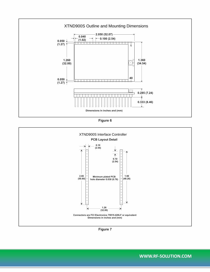
Figure 6
WWW.RF-SOLUTION.COM
XTND900S Outline and Mounting Dimensions
XTND900S Interface Controller