Embed Size (px)
Citation preview
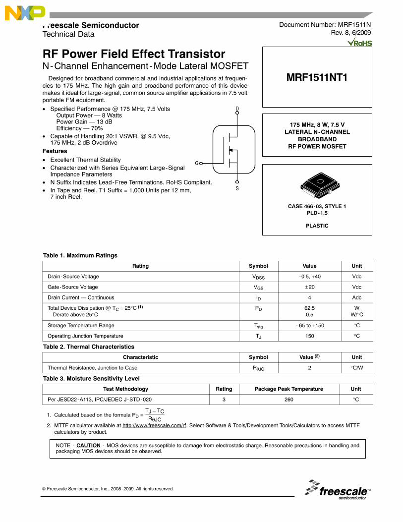
MRF1511NT1
1RF Device DataFreescale Semiconductor
RF Power Field Effect TransistorN-Channel Enhancement-Mode Lateral MOSFET
Designed for broadband commercial and industrial applications at frequen-cies to 175 MHz. The high gain and broadband performance of this devicemakes it ideal for large-signal, common source amplifier applications in 7.5 voltportable FM equipment.
• Specified Performance @ 175 MHz, 7.5 VoltsOutput Power � 8 WattsPower Gain � 13 dBEfficiency � 70%
• Capable of Handling 20:1 VSWR, @ 9.5 Vdc, 175 MHz, 2 dB Overdrive
Features• Excellent Thermal Stability• Characterized with Series Equivalent Large-Signal
Impedance Parameters• N Suffix Indicates Lead-Free Terminations. RoHS Compliant.• In Tape and Reel. T1 Suffix = 1,000 Units per 12 mm,
7 inch Reel.
Table 1. Maximum Ratings
Rating Symbol Value Unit
Drain-Source Voltage VDSS -0.5, +40 Vdc
Gate-Source Voltage VGS ±20 Vdc
Drain Current � Continuous ID 4 Adc
Total Device Dissipation @ TC = 25°C (1)
Derate above 25°CPD 62.5
0.5W
W/°C
Storage Temperature Range Tstg - 65 to +150 °C
Operating Junction Temperature TJ 150 °C
Table 2. Thermal Characteristics
Characteristic Symbol Value (2) Unit
Thermal Resistance, Junction to Case RθJC 2 °C/W
Table 3. Moisture Sensitivity Level
Test Methodology Rating Package Peak Temperature Unit
Per JESD22-A113, IPC/JEDEC J-STD-020 3 260 °C
1. Calculated based on the formula PD =
2. MTTF calculator available at http://www.freescale.com/rf. Select Software & Tools/Development Tools/Calculators to access MTTFcalculators by product.
NOTE - CAUTION - MOS devices are susceptible to damage from electrostatic charge. Reasonable precautions in handling andpackaging MOS devices should be observed.
Document Number: MRF1511NRev. 8, 6/2009
Freescale SemiconductorTechnical Data
MRF1511NT1
175 MHz, 8 W, 7.5 VLATERAL N-CHANNEL
BROADBANDRF POWER MOSFET
CASE 466-03, STYLE 1PLD-1.5
PLASTIC
G
D
S
TJ � TCRθJC
© Freescale Semiconductor, Inc., 2008-2009. All rights reserved.

2RF Device Data
Freescale Semiconductor
MRF1511NT1
Table 4. Electrical Characteristics (TA = 25°C unless otherwise noted)
Characteristic Symbol Min Typ Max Unit
Off Characteristics
Zero Gate Voltage Drain Current(VDS = 35 Vdc, VGS = 0)
IDSS � � 1 μAdc
Gate-Source Leakage Current(VGS = 10 Vdc, VDS = 0)
IGSS � � 1 μAdc
On Characteristics
Gate Threshold Voltage(VDS = 7.5 Vdc, ID = 170 μA)
VGS(th) 1 1.6 2.1 Vdc
Drain-Source On-Voltage(VGS = 10 Vdc, ID = 1 Adc)
VDS(on) � 0.4 � Vdc
Dynamic Characteristics
Input Capacitance(VDS = 7.5 Vdc, VGS = 0, f = 1 MHz)
Ciss � 100 � pF
Output Capacitance(VDS = 7.5 Vdc, VGS = 0, f = 1 MHz)
Coss � 53 � pF
Reverse Transfer Capacitance(VDS = 7.5 Vdc, VGS = 0, f = 1 MHz)
Crss � 8 � pF
Functional Tests (In Freescale Test Fixture)
Common-Source Amplifier Power Gain(VDD = 7.5 Vdc, Pout = 8 Watts, IDQ = 150 mA, f = 175 MHz)
Gps � 13 � dB
Drain Efficiency(VDD = 7.5 Vdc, Pout = 8 Watts, IDQ = 150 mA, f = 175 MHz)
η � 70 � %

MRF1511NT1
3RF Device DataFreescale Semiconductor
Figure 1. 135 - 175 MHz Broadband Test Circuit
VDD
C6 R4C7
C5
R3
RF
INPUT
RF
OUTPUTZ2 Z3
Z6
C1C3
C14DUT
Z7 Z9 Z10
Z4 Z5
L4
Z8N2
C18 B2
N1
+
C11
B1, B2 Short Ferrite Beads, Fair Rite Products (2743021446)
C1, C5, C18 120 pF, 100 mil Chip CapacitorsC2, C10, C12 0 to 20 pF, Trimmer CapacitorsC3 33 pF, 100 mil Chip CapacitorC4 68 pF, 100 mil Chip CapacitorC6, C15 10 μF, 50 V Electrolytic CapacitorsC7, C16 1,200 pF, 100 mil Chip CapacitorsC8, C17 0.1 μF, 100 mil Chip CapacitorsC9 150 pF, 100 mil Chip CapacitorC11 43 pF, 100 mil Chip CapacitorC13 24 pF, 100 mil Chip CapacitorC14 300 pF, 100 mil Chip CapacitorL1, L3 12.5 nH, A04T, CoilcraftL2 26 nH, 4 Turn, CoilcraftL4 55.5 nH, 5 Turn, CoilcraftN1, N2 Type N Flange Mounts
R1 15 Ω, 0805 Chip ResistorR2 1.0 kΩ, 1/8 W ResistorR3 1.0 kΩ, 0805 Chip ResistorR4 33 kΩ, 1/8 W ResistorZ1 0.200″ x 0.080″ MicrostripZ2 0.755″ x 0.080″ MicrostripZ3 0.300″ x 0.080″ MicrostripZ4 0.065″ x 0.080″ MicrostripZ5, Z6 0.260″ x 0.223″ MicrostripZ7 0.095″ x 0.080″ MicrostripZ8 0.418″ x 0.080″ MicrostripZ9 1.057″ x 0.080″ MicrostripZ10 0.120″ x 0.080″ MicrostripBoard Glass Teflon®, 31 mils, 2 oz. Copper
Z1
C2
R1
C4
VGG
C15+
C8B1
R2
C16C17
C9 C10 C13C12
L3
L2L1
TYPICAL CHARACTERISTICS, 135 - 175 MHz
175 MHz
155 MHz
135 MHz
Pout, OUTPUT POWER (WATTS)
IRL,
IN
PU
T R
ET
UR
N L
OS
S (
dB)
−5
−15
−20
−10
21 4 5
Figure 2. Output Power versus Input Power
Pin, INPUT POWER (WATTS)
2
Figure 3. Input Return Loss versus Output Power
0.3
P out
, O
UT
PU
T P
OW
ER
(W
AT
TS
)
0
8
0.50.1
4
0.4 0.70.20
10
30.6
6
VDD = 7.5 V
76 9 108
175 MHz
155 MHz
135 MHz
VDD = 7.5 V
−25

4RF Device Data
Freescale Semiconductor
MRF1511NT1
TYPICAL CHARACTERISTICS, 135 - 175 MHz
2
Pout, OUTPUT POWER (WATTS)
50
0
70
0 10
Eff,
DR
AIN
EF
FIC
IEN
CY
(%
)
30
60
40
31
Eff,
DR
AIN
EF
FIC
IEN
CY
(%
)
Figure 4. Gain versus Output Power
Pout, OUTPUT POWER (WATTS)
8
6
14
Figure 5. Drain Efficiency versus Output Power
2
GA
IN (
dB)
5
Figure 6. Output Power versus Biasing Current
12
IDQ, BIASING CURRENT (mA)
4
Figure 7. Drain Efficiency versusBiasing Current
80
IDQ, BIASING CURRENT (mA)
Figure 8. Output Power versus Supply Voltage
4
VDD, SUPPLY VOLTAGE (VOLTS)
2
Figure 9. Drain Efficiency versus Supply Voltage
VDD, SUPPLY VOLTAGE (VOLTS)
30148 4
0
40
60
70
404000
8
14
600 1000
80
5
6
10
10
16
200
50
4
12
P out
, O
UT
PU
T P
OW
ER
(W
AT
TS
)
200 1000400 600
P out
, O
UT
PU
T P
OW
ER
(W
AT
TS
)
6 14 1612 6 128 16
31
60
4
6
10
12
Eff,
DR
AIN
EF
FIC
IEN
CY
(%
)
50
70
4 75 86 9
20
10
175 MHz
155 MHz
135 MHz
VDD = 7.5 V
175 MHz
155 MHz
135 MHz
VDD = 7.5 V
7 10986
800
7
8
9
11
175 MHz
155 MHz
135 MHz
VDD = 7.5 V
Pin = 27 dBm
800
175 MHz
155 MHz
135 MHz
VDD = 7.5 V
Pin = 27 dBm
10
175 MHz
155 MHz
135 MHz
IDQ = 150 mA
Pin = 27 dBm
10
175 MHz
155 MHz
135 MHz
IDQ = 150 mA
Pin = 27 dBm
MRF1511NT1
5RF Device DataFreescale Semiconductor
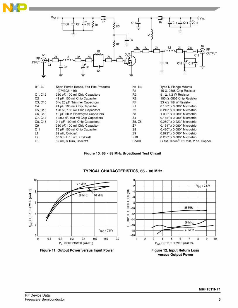
Figure 10. 66 - 88 MHz Broadband Test Circuit
VDD
C6 R4C7
C5
R3
RF
INPUT
RF
OUTPUTZ2 Z3
Z6
C1C3
C12DUT
Z7 Z9 Z10
Z4 Z5
L4
Z8N2
C16 B2
N1
+
C9
Z1
C2
R1
C4
VGG
C13+
C8B1
R2
C14C15
C11C10
L3
L1
B1, B2 Short Ferrite Beads, Fair Rite Products (2743021446)
C1, C12 330 pF, 100 mil Chip CapacitorsC2 43 pF, 100 mil Chip CapacitorC3, C10 0 to 20 pF, Trimmer CapacitorsC4 24 pF, 100 mil Chip CapacitorC5, C16 120 pF, 100 mil Chip CapacitorsC6, C13 10 μF, 50 V Electrolytic CapacitorsC7, C14 1,200 pF, 100 mil Chip CapacitorsC8, C15 0.1 μF, 100 mil Chip CapacitorsC9 380 pF, 100 mil Chip CapacitorC11 75 pF, 100 mil Chip CapacitorL1 82 nH, CoilcraftL2 55.5 nH, 5 Turn, CoilcraftL3 39 nH, 6 Turn, Coilcraft
N1, N2 Type N Flange MountsR1 15 Ω, 0805 Chip ResistorR2 51 Ω, 1/2 W ResistorR3 100 Ω, 0805 Chip ResistorR4 33 kΩ, 1/8 W ResistorZ1 0.136″ x 0.080″ MicrostripZ2 0.242″ x 0.080″ MicrostripZ3 1.032″ x 0.080″ MicrostripZ4 0.145″ x 0.080″ MicrostripZ5, Z6 0.260″ x 0.223″ MicrostripZ7 0.134″ x 0.080″ MicrostripZ8 0.490″ x 0.080″ MicrostripZ9 0.872″ x 0.080″ MicrostripZ10 0.206″ x 0.080″ MicrostripBoard Glass Teflon®, 31 mils, 2 oz. Copper
TYPICAL CHARACTERISTICS, 66 - 88 MHz
Pout, OUTPUT POWER (WATTS)
IRL,
IN
PU
T R
ET
UR
N L
OS
S (
dB)
−18
−20
−10
21
0
4 5
Figure 11. Output Power versus Input Power
Pin, INPUT POWER (WATTS)
2
Figure 12. Input Return Loss versus Output Power
0.3
P out
, O
UT
PU
T P
OW
ER
(W
AT
TS
)
0
6
0.50.1
4
0.4 0.70.20
10
30.6
8
66 MHz
77 MHz
88 MHz
VDD = 7.5 V
76 9 108
−14
−16
−12
−2
−6
−8
−4
66 MHz
77 MHz
88 MHz
VDD = 7.5 V
6RF Device Data
Freescale Semiconductor
MRF1511NT1
TYPICAL CHARACTERISTICS, 66 - 88 MHz
5
Pout, OUTPUT POWER (WATTS)
50
0
70
1 4
Eff,
DR
AIN
EF
FIC
IEN
CY
(%
)
30
60
40
32
Eff,
DR
AIN
EF
FIC
IEN
CY
(%
)
Figure 13. Gain versus Output Power
Pout, OUTPUT POWER (WATTS)
8
10
16
Figure 14. Drain Efficiency versusOutput Power
2
GA
IN (
dB)
1
Figure 15. Output Power versusBiasing Current
12
IDQ, BIASING CURRENT (mA)
4
Figure 16. Drain Efficiency versusBiasing Current
80
IDQ, BIASING CURRENT (mA)
Figure 17. Output Power versusSupply Voltage
5
VDD, SUPPLY VOLTAGE (VOLTS)
2
Figure 18. Drain Efficiency versusSupply Voltage
VDD, SUPPLY VOLTAGE (VOLTS)
98 5
0
40
60
60
404000
8
14
600 1000
80
6
8
10
12
18
200
50
4
14
P out
, O
UT
PU
T P
OW
ER
(W
AT
TS
)
200 1000400 600
P out
, O
UT
PU
T P
OW
ER
(W
AT
TS
)
6 9 107 6 7 8 10
3 5
4
6
10
12
Eff,
DR
AIN
EF
FIC
IEN
CY
(%
)
50
70
30
IDQ = 150 mA
Pin = 25.7 dBm
76 98 10
66 MHz
77 MHz
88 MHz
20
10
106 987
66 MHz77 MHz
88 MHz
800
5
11
7
9
66 MHz
77 MHz
88 MHz
VDD = 7.5 V
Pin = 25.7 dBm
VDD = 7.5 VVDD = 7.5 V
800
70
66 MHz
77 MHz
88 MHz
VDD = 7.5 V
Pin = 25.7 dBm
66 MHz
77 MHz
88 MHz
66 MHz
77 MHz
88 MHz
IDQ = 150 mA
Pin = 25.7 dBm
MRF1511NT1
7RF Device DataFreescale Semiconductor
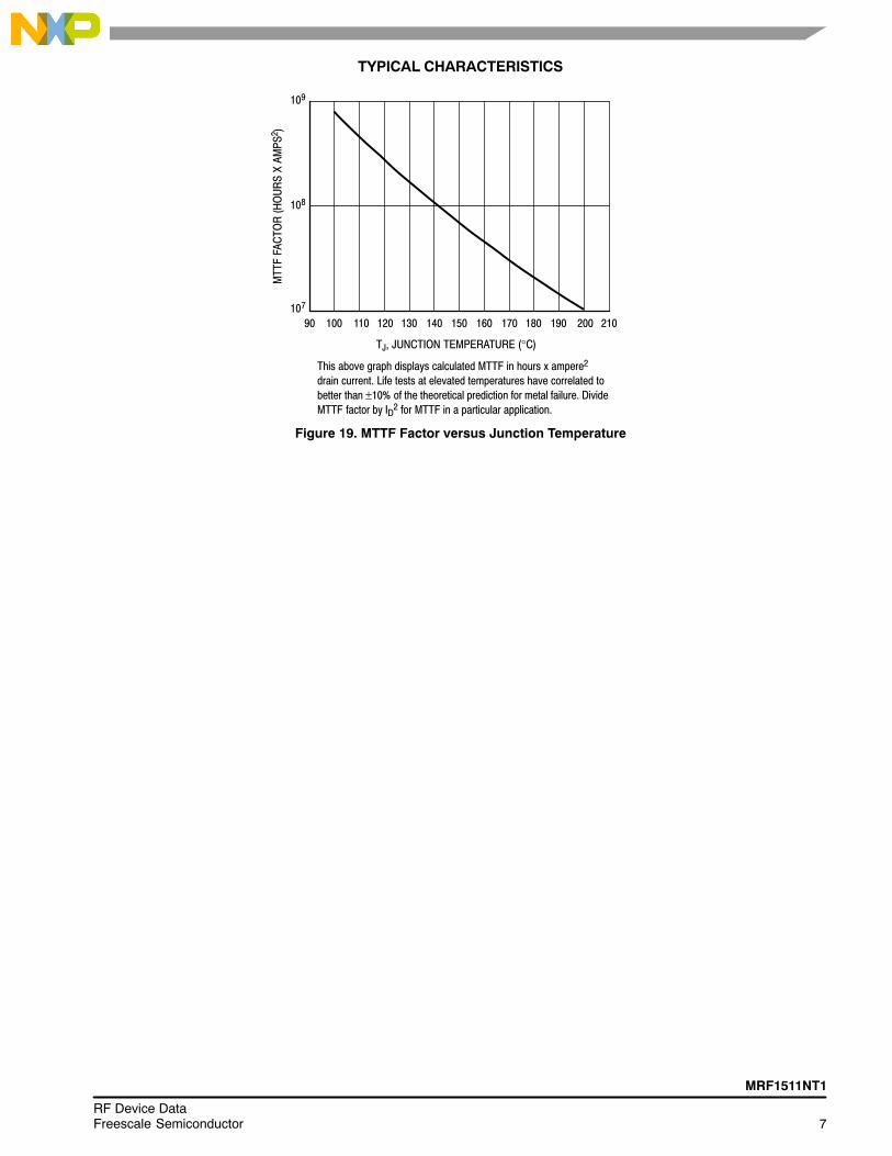
TYPICAL CHARACTERISTICS
210
109
TJ, JUNCTION TEMPERATURE (°C)
This above graph displays calculated MTTF in hours x ampere2
drain current. Life tests at elevated temperatures have correlated to
better than ±10% of the theoretical prediction for metal failure. Divide
MTTF factor by ID2 for MTTF in a particular application.
108
107
MT
TF
FA
CT
OR
(H
OU
RS
X A
MP
S2 )
90 110 130 150 170 190100 120 140 160 180 200
Figure 19. MTTF Factor versus Junction Temperature

8RF Device Data
Freescale Semiconductor
MRF1511NT1
Note: ZOL* was chosen based on tradeoffs between gain, drain efficiency, and device stability.
Figure 20. Series Equivalent Input and Output Impedance
Zo = 10 Ω
Zin = Complex conjugate of source impedance with parallel 15 Ω resistor and 24 pF capacitor in series with gate. (See Figure 10).
ZOL* = Complex conjugate of the load impedance at given output power,voltage, frequency, and ηD > 50 %.
fMHz
ZinΩ
ZOL*Ω
135 20.1 - j0.5 2.53 - j2.61
Zin = Complex conjugate of source impedance with parallel 15 Ω resistor and 68 pF capacitor in series with gate. (See Figure 1).
ZOL* = Complex conjugate of the load impedance at given output power, voltage, frequency, and ηD > 50 %.
VDD = 7.5 V, IDQ = 150 mA, Pout = 8 W
155 17.0 +j3.6 3.01 - j2.48
175 15.2 +j7.9 2.52 - j3.02
fMHz
ZinΩ
ZOL*Ω
66 25.3 - j0.31 3.62 - j0.751
VDD = 7.5 V, IDQ = 150 mA, Pout = 8 W
77 25.6 +j3.62 3.59 - j0.129
88 26.7 +j6.79 3.37 - j0.173
ZOL*
Zin
135
155
f = 175 MHz
135
155f = 175 MHz
6677
Zin
f = 88 MHz
66
77f = 88 MHz
ZOL*
Zin
ZOL
*
Input
Matching
Network
Device
Under Test
Output
Matching
Network

MRF1511NT1
9RF Device DataFreescale Semiconductor
Table 5. Common Source Scattering Parameters (VDD = 7.5 Vdc)
IDQ = 150 mA
fS11 S21 S12 S22f
MHz |S11| ∠ φ |S21| ∠ φ |S12| ∠ φ |S22| ∠ φ
30 0.88 -165 18.92 95 0.015 8 0.84 -169
50 0.88 -171 11.47 91 0.016 -5 0.84 -173
100 0.87 -175 5.66 85 0.016 -7 0.84 -176
150 0.87 -176 3.75 82 0.015 -5 0.85 -176
200 0.87 -177 2.78 78 0.014 -6 0.84 -176
250 0.87 -177 2.16 75 0.014 -10 0.85 -176
300 0.88 -177 1.77 72 0.012 -17 0.86 -176
350 0.88 -177 1.49 69 0.013 -11 0.86 -176
400 0.88 -177 1.26 66 0.013 -17 0.87 -175
450 0.88 -177 1.08 64 0.011 -20 0.87 -175
500 0.89 -176 0.96 63 0.012 -20 0.88 -175
IDQ = 800 mA
fS11 S21 S12 S22f
MHz |S11| ∠ φ |S21| ∠ φ |S12| ∠ φ |S22| ∠ φ
30 0.89 -166 18.89 95 0.014 10 0.85 -170
50 0.88 -172 11.44 91 0.015 8 0.84 -174
100 0.87 -175 5.65 86 0.016 -2 0.85 -176
150 0.87 -177 3.74 82 0.014 -8 0.84 -177
200 0.87 -177 2.78 78 0.013 -18 0.85 -177
250 0.88 -177 2.16 75 0.012 -11 0.85 -176
300 0.88 -177 1.77 73 0.015 -15 0.86 -176
350 0.88 -177 1.50 70 0.009 -7 0.87 -176
400 0.88 -177 1.26 67 0.012 -3 0.87 -176
450 0.88 -177 1.09 65 0.012 -18 0.87 -175
500 0.89 -177 0.97 64 0.009 -10 0.88 -175
IDQ = 1.5 A
fS11 S21 S12 S22f
MHz |S11| ∠ φ |S21| ∠ φ |S12| ∠ φ |S22| ∠ φ
30 0.90 -168 17.89 95 0.013 2 0.86 -172
50 0.89 -173 10.76 91 0.013 3 0.86 -175
100 0.88 -176 5.32 86 0.014 -19 0.86 -177
150 0.88 -177 3.53 83 0.013 -6 0.86 -177
200 0.88 -177 2.63 80 0.011 -4 0.86 -177
250 0.88 -178 2.05 77 0.012 -14 0.86 -177
300 0.88 -177 1.69 75 0.013 -2 0.87 -177
350 0.89 -177 1.43 72 0.010 -9 0.87 -176
400 0.89 -177 1.22 70 0.014 -3 0.88 -176
450 0.89 -177 1.06 68 0.011 -8 0.88 -176
500 0.89 -177 0.94 67 0.011 -15 0.88 -176

10RF Device Data
Freescale Semiconductor
MRF1511NT1
APPLICATIONS INFORMATION
DESIGN CONSIDERATIONSThis device is a common-source, RF power, N-Channel
enhancement mode, Lateral Metal -Oxide SemiconductorField -Effect Transistor (MOSFET). Freescale ApplicationNote AN211A, �FETs in Theory and Practice�, is suggestedreading for those not familiar with the construction and char-acteristics of FETs.
This surface mount packaged device was designed pri-marily for VHF and UHF portable power amplifier applica-tions. Manufacturability is improved by utilizing the tape andreel capability for fully automated pick and placement ofparts. However, care should be taken in the design processto insure proper heat sinking of the device.
The major advantages of Lateral RF power MOSFETs in-clude high gain, simple bias systems, relative immunity fromthermal runaway, and the ability to withstand severely mis-matched loads without suffering damage.
MOSFET CAPACITANCESThe physical structure of a MOSFET results in capacitors
between all three terminals. The metal oxide gate structuredetermines the capacitors from gate - to -drain (Cgd), andgate- to-source (Cgs). The PN junction formed during fab-rication of the RF MOSFET results in a junction capacitancefrom drain- to-source (Cds). These capacitances are charac-terized as input (Ciss), output (Coss) and reverse transfer(Crss) capacitances on data sheets. The relationships be-tween the inter- terminal capacitances and those given ondata sheets are shown below. The Ciss can be specified intwo ways:
1. Drain shorted to source and positive voltage at the gate.
2. Positive voltage of the drain in respect to source and zerovolts at the gate.
In the latter case, the numbers are lower. However, neithermethod represents the actual operating conditions in RF ap-plications.
Drain
Cds
Source
Gate
Cgd
Cgs
Ciss = Cgd + Cgs
Coss = Cgd + Cds
Crss = Cgd
DRAIN CHARACTERISTICSOne critical figure of merit for a FET is its static resistance
in the full -on condition. This on-resistance, RDS(on), occursin the linear region of the output characteristic and is speci-fied at a specific gate-source voltage and drain current. The
drain -source voltage under these conditions is termedVDS(on). For MOSFETs, VDS(on) has a positive temperaturecoefficient at high temperatures because it contributes to thepower dissipation within the device.
BVDSS values for this device are higher than normally re-quired for typical applications. Measurement of BVDSS is notrecommended and may result in possible damage to the de-vice.
GATE CHARACTERISTICSThe gate of the RF MOSFET is a polysilicon material, and
is electrically isolated from the source by a layer of oxide.The DC input resistance is very high - on the order of 109 Ω� resulting in a leakage current of a few nanoamperes.
Gate control is achieved by applying a positive voltage tothe gate greater than the gate- to-source threshold voltage,VGS(th).
Gate Voltage Rating � Never exceed the gate voltagerating. Exceeding the rated VGS can result in permanentdamage to the oxide layer in the gate region.
Gate Termination � The gates of these devices are es-sentially capacitors. Circuits that leave the gate open-cir-cuited or floating should be avoided. These conditions canresult in turn-on of the devices due to voltage build-up onthe input capacitor due to leakage currents or pickup.
Gate Protection � These devices do not have an internalmonolithic zener diode from gate- to-source. If gate protec-tion is required, an external zener diode is recommended.Using a resistor to keep the gate- to-source impedance lowalso helps dampen transients and serves another importantfunction. Voltage transients on the drain can be coupled tothe gate through the parasitic gate-drain capacitance. If thegate- to-source impedance and the rate of voltage changeon the drain are both high, then the signal coupled to the gatemay be large enough to exceed the gate- threshold voltageand turn the device on.DC BIAS
Since this device is an enhancement mode FET, drain cur-rent flows only when the gate is at a higher potential than thesource. RF power FETs operate optimally with a quiescentdrain current (IDQ), whose value is application dependent.This device was characterized at IDQ = 150 mA, which is thesuggested value of bias current for typical applications. Forspecial applications such as linear amplification, IDQ mayhave to be selected to optimize the critical parameters.
The gate is a dc open circuit and draws no current. There-fore, the gate bias circuit may generally be just a simple re-sistive divider network. Some special applications mayrequire a more elaborate bias system.GAIN CONTROL
Power output of this device may be controlled to some de-gree with a low power dc control signal applied to the gate,thus facilitating applications such as manual gain control,ALC/AGC and modulation systems. This characteristic isvery dependent on frequency and load line.

MRF1511NT1
11RF Device DataFreescale Semiconductor
MOUNTINGThe specified maximum thermal resistance of 2°C/W as-
sumes a majority of the 0.065″ x 0.180″ source contact onthe back side of the package is in good contact with an ap-propriate heat sink. As with all RF power devices, the goal ofthe thermal design should be to minimize the temperature atthe back side of the package. Refer to Freescale ApplicationNote AN4005/D, �Thermal Management and Mounting Meth-od for the PLD-1.5 RF Power Surface Mount Package,� andEngineering Bulletin EB209/D, �Mounting Method for RFPower Leadless Surface Mount Transistor� for additional in-formation.AMPLIFIER DESIGN
Impedance matching networks similar to those used withbipolar transistors are suitable for this device. For examplessee Freescale Application Note AN721, �ImpedanceMatching Networks Applied to RF Power Transistors.�
Large-signal impedances are provided, and will yield a goodfirst pass approximation.
Since RF power MOSFETs are triode devices, they are notunilateral. This coupled with the very high gain of this deviceyields a device capable of self oscillation. Stability may beachieved by techniques such as drain loading, input shuntresistive loading, or output to input feedback. The RF test fix-ture implements a parallel resistor and capacitor in serieswith the gate, and has a load line selected for a higher effi-ciency, lower gain, and more stable operating region.
Two - port stabi l i ty analysis with this device�sS-parameters provides a useful tool for selection of loadingor feedback circuitry to assure stable operation. See Free-scale Application Note AN215A, �RF Small -Signal DesignUsing Two-Port Parameters� for a discussion of two portnetwork theory and stability.
12RF Device Data
Freescale Semiconductor
MRF1511NT1
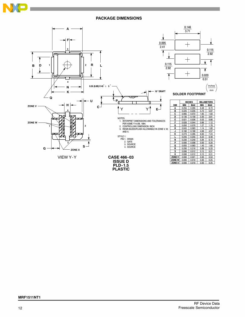
PACKAGE DIMENSIONS
0.115
2.92
0.020
0.51
0.115
2.92
mm
inches
0.095
2.41
0.146
3.71
SOLDER FOOTPRINT
CASE 466-03ISSUE D
NOTES:1. INTERPRET DIMENSIONS AND TOLERANCES
PER ASME Y14.5M, 1984.2. CONTROLLING DIMENSION: INCH3. RESIN BLEED/FLASH ALLOWABLE IN ZONE V, W,
AND X.
DIM MIN MAX MIN MAX
MILLIMETERSINCHES
A 0.255 0.265 6.48 6.73
B 0.225 0.235 5.72 5.97
C 0.065 0.072 1.65 1.83
D 0.130 0.150 3.30 3.81
E 0.021 0.026 0.53 0.66
F 0.026 0.044 0.66 1.12
G 0.050 0.070 1.27 1.78
H 0.045 0.063 1.14 1.60
K 0.273 0.285 6.93 7.24
L 0.245 0.255 6.22 6.48
N 0.230 0.240 5.84 6.10
P 0.000 0.008 0.00 0.20
Q 0.055 0.063 1.40 1.60
R 0.200 0.210 5.08 5.33
S 0.006 0.012 0.15 0.31
U 0.006 0.012 0.15 0.31
ZONE V 0.000 0.021 0.00 0.53
ZONE W 0.000 0.010 0.00 0.25
ZONE X 0.000 0.010 0.00 0.25
STYLE 1:PIN 1. DRAIN
2. GATE 3. SOURCE 4. SOURCE
J 0.160 0.180 4.06 4.57
ÉÉÉÉÉÉÉÉÉÉÉÉÉÉÉ
ÉÉÉÉÉÉÉÉÉÉÉÉÉÉÉ
ÉÉÉÉÉÉÉÉÉÉ
A
B D
F
LR
3
4
21
KN
ZONE V
ZONE W
ZONE XGS
HU
�10 DRAFT
P
CE
0.35 (0.89) X 45 5�
Y Y
Q
VIEW Y-Y
� �
4
21
3
PLD-1.5PLASTIC

MRF1511NT1
13RF Device DataFreescale Semiconductor
PRODUCT DOCUMENTATION, TOOLS AND SOFTWARE
Refer to the following documents to aid your design process.
Application Notes
• AN211A: Field Effect Transistors in Theory and Practice
• AN215A: RF Small -Signal Design Using Two-Port Parameters
• AN721: Impedance Matching Networks Applied to RF Power Transistors
• AN4005: Thermal Management and Mounting Method for the PLD 1.5 RF Power Surface Mount Package
Engineering Bulletins• EB212: Using Data Sheet Impedances for RF LDMOS Devices
Software• Electromigration MTTF Calculator
For Software and Tools, do a Part Number search at http://www.freescale.com, and select the �Part Number� link. Go to theSoftware & Tools tab on the part�s Product Summary page to download the respective tool.
REVISION HISTORY
The following table summarizes revisions to this document.
Revision Date Description
7 June 2008 • Corrected specified performance values for power gain and efficiency on p. 1 to match typicalperformance values in the functional test table on p. 2
• Added Product Documentation and Revision History, p. 13
8 June 2009 • Modified data sheet to reflect MSL rating change from 1 to 3 as a result of the standardization of packingprocess as described in Product and Process Change Notification number, PCN13516, p. 1
• Added Electromigration MTTF Calculator availability to Product Documentation, Tools and Software, p. 13

14RF Device Data
Freescale Semiconductor
MRF1511NT1
How to Reach Us:
Home Page:www.freescale.com
Web Support:http://www.freescale.com/support
USA/Europe or Locations Not Listed:Freescale Semiconductor, Inc.Technical Information Center, EL5162100 East Elliot RoadTempe, Arizona 852841-800-521-6274 or +1-480-768-2130www.freescale.com/support
Europe, Middle East, and Africa:Freescale Halbleiter Deutschland GmbHTechnical Information CenterSchatzbogen 781829 Muenchen, Germany+44 1296 380 456 (English)+46 8 52200080 (English)+49 89 92103 559 (German)+33 1 69 35 48 48 (French)www.freescale.com/support
Japan:Freescale Semiconductor Japan Ltd.HeadquartersARCO Tower 15F1-8-1, Shimo-Meguro, Meguro-ku,Tokyo 153-0064Japan0120 191014 or +81 3 5437 [email protected]
Asia/Pacific:Freescale Semiconductor China Ltd.Exchange Building 23FNo. 118 Jianguo RoadChaoyang DistrictBeijing 100022 China +86 10 5879 [email protected]
For Literature Requests Only:Freescale Semiconductor Literature Distribution Center1-800-441-2447 or +1-303-675-2140Fax: [email protected]
Information in this document is provided solely to enable system and softwareimplementers to use Freescale Semiconductor products. There are no express orimplied copyright licenses granted hereunder to design or fabricate any integratedcircuits or integrated circuits based on the information in this document.
Freescale Semiconductor reserves the right to make changes without further notice toany products herein. Freescale Semiconductor makes no warranty, representation orguarantee regarding the suitability of its products for any particular purpose, nor doesFreescale Semiconductor assume any liability arising out of the application or use ofany product or circuit, and specifically disclaims any and all liability, including withoutlimitation consequential or incidental damages. �Typical� parameters that may beprovided in Freescale Semiconductor data sheets and/or specifications can and dovary in different applications and actual performance may vary over time. All operatingparameters, including �Typicals�, must be validated for each customer application bycustomer�s technical experts. Freescale Semiconductor does not convey any licenseunder its patent rights nor the rights of others. Freescale Semiconductor products arenot designed, intended, or authorized for use as components in systems intended forsurgical implant into the body, or other applications intended to support or sustain life,or for any other application in which the failure of the Freescale Semiconductor productcould create a situation where personal injury or death may occur. Should Buyerpurchase or use Freescale Semiconductor products for any such unintended orunauthorized application, Buyer shall indemnify and hold Freescale Semiconductorand its officers, employees, subsidiaries, affiliates, and distributors harmless against allclaims, costs, damages, and expenses, and reasonable attorney fees arising out of,directly or indirectly, any claim of personal injury or death associated with suchunintended or unauthorized use, even if such claim alleges that FreescaleSemiconductor was negligent regarding the design or manufacture of the part.
Freescale� and the Freescale logo are trademarks of Freescale Semiconductor, Inc.All other product or service names are the property of their respective owners.© Freescale Semiconductor, Inc. 2008-2009. All rights reserved.
Document Number: MRF1511NRev. 8, 6/2009
RoHS-compliant and/or Pb-free versions of Freescale products have the functionality and electricalcharacteristics of their non-RoHS-compliant and/or non-Pb-free counterparts. For furtherinformation, see http://www.freescale.com or contact your Freescale sales representative.
For information on Freescale�s Environmental Products program, go to http://www.freescale.com/epp.