Embed Size (px)
Citation preview
RF Front-End Design for X Band using 0.15µm GaN HEMT
Technology
Sumit Saha
A thesis presented to Ottawa-Carleton Institute
for Electrical and Computer Engineering
in partial fulfillment to the thesis requirement for the degree of
MASTER OF APPLIED SCIENCE
in
ELECTRICAL AND COMPUTER ENGINEERING
University of Ottawa
Ottawa, ON, Canada
April 2016
© Sumit Saha, Ottawa, Canada, 2016
- ii -
ABSTRACT
The primary reason for the wireless technology evolution is towards building capacity and obtaining
higher data rates. Enclosed locations, densely populated campus, indoor offices, and device-to-device
communication will require radios that need to operate at data rates up to 10 Gbps. In the next few
years, a new generation of communication systems would emerge to better handle the ever-increasing
demand for much wider bandwidth requirements. Simultaneously, key factors such as size, cost, and
energy consumption play a distinctive role towards shaping the success of future wireless
technologies. In the perspective of 3GPP 5G next generation wireless communication systems, the X
band was explicitly targeted with a vast range of applications in point to point radio, point to multi
point radio, test equipment, sensors and future wireless communication.
An X-band RF front-end circuit for next generation wireless network applications is presented in this
work. It details the design of a low noise amplifier and a power amplifier for X band operation. The
designed amplifiers were integrated with a wideband single-pole-double-throw switch to achieve an
overall front-end structure for 10 GHz. The design was carried out and sent for fabrication using a
GaN 0.15µm process provided by NRC, a novel design kit. Due to higher breakdown voltage, high
power density, high efficiency, high linearity and better noise performance, GaN HEMTs are a
suitable choice for future wireless communication. Thus, the assumption is to further explore
capabilities of this process in front-end design for future wireless communications.

- iii -
ACKNOWLEDGEMENTS
I would like to acknowledge the efforts of several individuals without whom this thesis would not
have been possible.
Firstly, I would like to thank my supervisor Dr. Mustapha C.E. Yagoub for all his advice, supervision,
inspiration and guidance throughout this learning process. I have been fortunate to have a supervisor
who gave me the freedom to explore on my own and guide me in the right direction. He made himself
always available whenever I had questions and continuously provided support throughout this thesis
process. His commitment towards my research work will always be appreciated.
Secondly, I want to express my deepest gratitude to my co-supervisor Dr. Rony Amaya for the
countless hours of support, and direction that he has provided for this project over the last year. The
research work was greatly inspired from his area of expertise and I appreciate him very much for
sharing it. Dr. Amaya had a very crucial role towards helping me sort out the technical details of this
research project for which I am eternally grateful.
In addition, I am thankful to Blackberry and my manager Michael Bo for their moral and financial
support towards this project. Without them, the completion of this thesis would not have been
possible.
Last, but not least, no acknowledgement is complete without expressing gratitude and thankfulness
towards one’s family. They have been through the best and worst of times with me and I would like
to deeply thank them for their support and faith in me. A special mention to my wife (Rebecca Paul)
and mother (Dr. Bandana Saha) for their persistent confidence in me, which has given me that extra
boost to complete this long endeavor.
- iv -
TABLE OF CONTENTS
ABSTRACT ................................................................................................................................................................. II
ACKNOWLEDGEMENTS ........................................................................................................................................... III
TABLE OF CONTENTS ............................................................................................................................................. IV
LIST OF FIGURES ..................................................................................................................................................... VI
LIST OF TABLES........................................................................................................................................................IX
LIST OF ACRONYMS AND ABBREVIATIONS ............................................................................................................X
LIST OF VARIABLES .................................................................................................................................................XI
CHAPTER 1 INTRODUCTION .................................................................................................................................... 1
1.1 MOTIVATIONS ........................................................................................................................................................... 1 1.2 RF FRONT-END ISSUES ............................................................................................................................................... 2 1.3 THESIS CONTRIBUTION .............................................................................................................................................. 4 1.4 THESIS ORGANIZATION .............................................................................................................................................. 4
CHAPTER 2 DESIGN CONSIDERATIONS .................................................................................................................. 6
2.1 INTRODUCTION ......................................................................................................................................................... 6 2.2 FRONT-END CONFIGURATION ................................................................................................................................... 6 2.3 TECHNOLOGY SELECTION .......................................................................................................................................... 7 2.4 GAN LIMITATIONS .................................................................................................................................................... 10 2.5 GAN FOUNDRY PROCESS ......................................................................................................................................... 11 2.6 CONCLUSION ........................................................................................................................................................... 11
CHAPTER 3 LNA DESIGN PRINCIPLES ................................................................................................................... 13
3.1 DEFINITIONS AND KEY DESIGN PARAMETERS .......................................................................................................... 13 3.2 TWO PORT S-PARAMETERS...................................................................................................................................... 14
3.2.1 POWER MATCHING .................................................................................................................................. 15 3.2.2 GAIN ............................................................................................................................................................. 16
3.3 NOISE ....................................................................................................................................................................... 16 3.4 STABILITY ................................................................................................................................................................. 17 3.5 LINEARITY OVERVIEW .............................................................................................................................................. 18
3.5.1 1- dB COMPRESSION POINT ................................................................................................................. 18 3.5.2 HARMONICS, IMD AND INTERCEPT POINT ...................................................................................... 19
3.6 POPULAR WIDEBAND LNA TOPOLOGIES .................................................................................................................. 20 3.7 CONCLUSION ........................................................................................................................................................... 21
CHAPTER 4 LOW NOISE AMPLIFIER DESIGN ....................................................................................................... 22
4.1 REQUIREMENT OF X BAND LOW NOISE AMPLIFIER ................................................................................................. 22 4.2 LITERATURE REVIEW ................................................................................................................................................ 22 4.3 RESISTIVE FEEDBACK LOW NOISE AMPLIFIER DESIGN ............................................................................................. 24
4.3.1 SHUNT RESISTIVE FEEDBACK ESTIMATION ................................................................................ 26 4.3.2 DESIGN PROCEDURE ........................................................................................................................... 28 4.3.3 FEEDBACK RESISTANCE CALCULATION AND DEVICE SIZING .............................................. 29 4.3.4 DC ANALYSIS .......................................................................................................................................... 29 4.3.5 TRANSISTOR HIGH FREQUENCY MODELLING ............................................................................. 31
4.4 SCHEMATIC DESIGN AND RESULT ............................................................................................................................ 34
- v -
4.5 LAYOUT DESIGN ....................................................................................................................................................... 44 4.5.1 BIAS NETWORK DESIGN ........................................................................................................................ 49 4.5.2 SIMULATION RESULT LAYOUT ............................................................................................................. 51
4.6 DISCUSSIONS AND CONCLUSION ............................................................................................................................. 57
CHAPTER 5 POWER AMPLIFIER BACKGROUND .................................................................................................. 60
5.1 DEFINITION AND KEY DESIGN PARAMETER ............................................................................................................. 60 5.2 CLASSES OF OPERATION .......................................................................................................................................... 60
5.2.1 CLASS A ...................................................................................................................................................... 61 5.2.2 CLASS B ...................................................................................................................................................... 62 5.2.3 CLASS C ...................................................................................................................................................... 62 5.2.4 CLASS AB ................................................................................................................................................... 62 5.2.5 ADDITIONAL POWER CLASSES ........................................................................................................... 63
5.3 POWER AMPLIFIER PERFORMANCE METRICS .......................................................................................................... 63 5.4 CONCLUSION ........................................................................................................................................................... 64
CHAPTER 6 X BAND POWER AMPLIFIER DESIGN ................................................................................................ 65
6.1 REQUIREMENTS OF X BAND POWER AMPLIFIER ...................................................................................................... 65 6.2 LITERATURE REVIEW ................................................................................................................................................ 66 6.3 DESIGN PROCEDURE ................................................................................................................................................ 66 6.4 DEVICE SIZING .......................................................................................................................................................... 67 6.5 DC ANALYSIS ............................................................................................................................................................ 67 6.6 SCHEMATIC DESIGN & SIMULATION ........................................................................................................................ 70
6.6.1 BIAS VOLTAGE OPTIMIZATION ............................................................................................................ 72 6.6.2 OPTIMUM LOAD SELECTION................................................................................................................. 74
6.7 LAYOUT DESIGN ....................................................................................................................................................... 77 6.7.1 BIAS NETWORK DESIGN ........................................................................................................................ 78 6.7.2 SIMULATION RESULT LAYOUT ............................................................................................................. 79
6.8 DISCUSSIONS AND CONCLUSION ............................................................................................................................. 87
CHAPTER 7 10 GHZ FRONT-END DESIGN ............................................................................................................. 89
7.1 WIDEBAND SWITCH ................................................................................................................................................. 89 7.2 LAYOUT DESIGN FOR 10 GHZ FRONT-END AND RESULT .......................................................................................... 93 7.3 DISCUSSIONS AND CONCLUSION ............................................................................................................................. 98
CHAPTER 8 CONCLUSION AND FUTURE WORK ................................................................................................. 100
8.1 CONCLUSION ......................................................................................................................................................... 100 8.2 FUTURE WORK ....................................................................................................................................................... 101
REFERENCES .......................................................................................................................................................... 102

- vi -
LIST OF FIGURES
FIGURE 1 TYPICAL FRONT-END ARCHITECTURE [15] ........................................................................................................................ 2 FIGURE 2 (A) GAAS FRONT-END (B) GAN FRONT-END [15] ............................................................................................................. 7 FIGURE 3 CLASSIFICATION OF TRANSISTORS [25] ............................................................................................................................ 8 FIGURE 4 TRAPPING EFFECT IN GAN [35] .................................................................................................................................... 10 FIGURE 5 DEVICE CROSS SECTION OF GAN 150 HFET [18] ............................................................................................................ 11 FIGURE 6 CROSS-SECTIONAL VIEW OF GAN150 HFET SHOWING PROCESS SEQUENCE [18] .................................................................. 12 FIGURE 7 TWO-PORT NETWORK SHOWING INCIDENT AND REFLECTED WAVES [37] .............................................................................. 14 FIGURE 8 TYPICAL 1 STAGE AMPLIFIER WITH INPUT AND OUTPUT MATCHING NETWORK [37] ................................................................. 16 FIGURE 9 1-DB COMPRESSION POINT, IIP3 & IIP2 [16] ................................................................................................................ 19 FIGURE 10 FUNDAMENTAL AND IMD TONES [16] ........................................................................................................................ 19 FIGURE 11 POPULAR WIDE BAND AMPLIFIER TOPOLOGIES [42] ....................................................................................................... 20 FIGURE 12 HIGH FREQUENCY MODEL OF A SHUNT RESISTIVE FEEDBACK TOPOLOGY [55] .................................................................... 25 FIGURE 13 2-STAGE X BAND AMPLIFIER TOPOLOGY USED IN [10] ..................................................................................................... 25 FIGURE 14 DESIGNED FEEDBACK TOPOLOGY [55] ......................................................................................................................... 26 FIGURE 15 LOW FREQUENCY SMALL SIGNAL MODEL FOR SHUNT FEEDBACK TOPOLOGY [55] ................................................................. 26 FIGURE 16 DRAIN CURRENT VS GATE VOLTAGE FOR 160µM X 2 GAN150 HFET ............................................................................... 30 FIGURE 17 THE RATIO OF DRAIN CURRENT VS SATURATED CURRENT OVER GATE VOLTAGE .................................................................. 30 FIGURE 18 UNITY GAIN FREQUENCY AND MAXIMUM FREQUENCY VS RATIO OF DRAIN CURRENT AND SATURATION CURRENT ..................... 31 FIGURE 19 TRANSCONDUCTANCE OF 160µM X 2 GAN150 HFET @ 15% SATURATION CURRENT BIAS POINT VS FREQUENCY ................... 32 FIGURE 20 GATE TO DRAIN AND DRAIN TO SOURCE CAPACITANCE VS FREQUENCY .............................................................................. 32 FIGURE 21 DRAIN TO SOURCE & INPUT RESISTANCE & GATE TO SOURCE CAPACITANCE VS FREQUENCY................................................... 33 FIGURE 22 BASIC SCHEMATIC OF 2 STAGE SHUNT FEEDBACK AMPLIFIER ........................................................................................... 35 FIGURE 23 (A) S(2, 1) AND MAX GAIN (B) S(1,1) AND (C) S(2,2) SIMULATION RESULT VARYING FEEDBACK RESISTOR (150 Ω TO 300 Ω) .. 36 FIGURE 24 NOISE FIGURE SIMULATION VARYING FEEDBACK RESISTANCE VALUE (150 Ω TO 300 Ω) ....................................................... 36 FIGURE 25 CHARACTERIZATION OF GAN KIT NICROME RESISTOR..................................................................................................... 37 FIGURE 26 ADS LAYOUT DRIVEN SCHEMATIC OF LOW NOISE AMPLIFIER .......................................................................................... 38 FIGURE 27 MAX GAIN AND S(2,1) VS FREQUENCY VARYING FEEDBACK INDUCTANCE (0.1 NH TO 1NH) .................................................. 39 FIGURE 28 S(1,1) VS FREQUENCY VARYING FEEDBACK INDUCTANCE (0.1 NH TO 1NH) ........................................................................ 39 FIGURE 29 S(2,2) VS FREQUENCY VARYING FEEDBACK INDUCTANCE (0.1 NH TO 1NH) ........................................................................ 39 FIGURE 30 MAX GAIN AND S (2, 1) VS FREQUENCY VARYING DRAIN INDUCTANCE (.01 NH TO .05NH) ................................................... 40 FIGURE 31 (A) S(1,1) (B) S(2,2) VS FREQUENCY VARYING DRAIN INDUCTANCE (.01 NH TO .05NH) ....................................................... 40 FIGURE 32 (A) FEEDBACK INDUCTANCE (B) RESISTANCE VS FREQUENCY ACHIEVED BY METAL1 CONNECTION ............................................ 40 FIGURE 33 (A) DRAIN INDUCTANCE (B) RESISTANCE VS FREQUENCY ACHIEVED BY METAL1 CONNECTION ................................................. 41 FIGURE 34 MAX GAIN AND S(2,1) VS FREQUENCY ........................................................................................................................ 42 FIGURE 35 S(1,1) VS FREQUENCY .............................................................................................................................................. 42 FIGURE 36 S(2,2) VS FREQUENCY .............................................................................................................................................. 43 FIGURE 37 THERMAL NOISE VS FREQUENCY ................................................................................................................................. 43 FIGURE 38 LNA LAYOUT DESIGN (AREA INCLUDING PADS 2.047 MM X 0.9 MM) .......................................................................... 44 FIGURE 39 LAYOUT DESIGN OF 160µM X 2 GAN150 HFET ........................................................................................................... 45 FIGURE 40 THROUGH WAFER VIA (TWV) ................................................................................................................................... 46 FIGURE 41 FEEDBACK LAYOUT DESIGN ....................................................................................................................................... 47 FIGURE 42 (A) FEEDBACK INDUCTANCE (B) RESISTANCE VS FREQUENCY IN LAYOUT DESIGN ................................................................... 47 FIGURE 43 MIM CAPACITOR FROM GAN150 DESIGN KIT ............................................................................................................. 48 FIGURE 44 NICROME RESISTOR FROM GAN150 DESIGN KIT .......................................................................................................... 48 FIGURE 45 DC PADS USED FOR LNA DESIGN ............................................................................................................................... 49 FIGURE 46 SIGNAL PADS USED IN LNA DESIGN ............................................................................................................................ 49 FIGURE 47 RADIAL STUB .......................................................................................................................................................... 50 FIGURE 48 EM SIMULATION SETUP FOR LNA LAYOUT DESIGN ........................................................................................................ 51

- vii -
FIGURE 49 MAX GAIN AND S(2,1) VS FREQUENCY ( 5GHZ TO 40 GHZ) ........................................................................................... 52 FIGURE 50 MAX GAIN AND S(2,1) VS FREQUENCY (7 GHZ TO 16 GHZ) ........................................................................................... 52 FIGURE 51 S(1,1) VS FREQUENCY .............................................................................................................................................. 53 FIGURE 52 S(2,2) VS FREQUENCY .............................................................................................................................................. 53 FIGURE 53 STABILITY FACTOR (K) VS FREQUENCY.......................................................................................................................... 54 FIGURE 54 STABILITY MEASURE (B) VS FREQUENCY ....................................................................................................................... 54 FIGURE 55 NOISE FIGURE (THERMAL) VS FREQUENCY .................................................................................................................... 55 FIGURE 56 GAIN VS FUNDAMENTAL OUTPUT POWER @10 GHZ .................................................................................................... 56 FIGURE 57 HIGH AND LOW SIDE THIRD ORDER IMD VS FUNDAMENTAL OUTPUT POWER BOTH TONES (DBC) ......................................... 56 FIGURE 58 HIGH AND LOW SIDE FIFTH ORDER IMD (DBC) VS FUNDAMENTAL OUTPUT POWER BOTH TONES .......................................... 56 FIGURE 59 THIRD ORDER INTERCEPT POINT ................................................................................................................................. 57 FIGURE 60 LOAD LINES FOR POWER AMPLIFIER CLASSES [62] ......................................................................................................... 61 FIGURE 61 DRAIN CURRENT VS GATE VOLTAGE WITH 20 V DRAIN SUPPLY VOLTAGE........................................................................... 68 FIGURE 62 DRAIN CURRENT VS GATE VOLTAGE FOR DIFFERENT GATE VOLTAGE ................................................................................. 69 FIGURE 63 DRAIN CURRENT VS GATE VOLTAGE WITH 20 V DC SUPPLY............................................................................................. 69 FIGURE 64 UNITY GAIN FREQUENCY VS RATIO OF DRAIN CURRENT AND SATURATED CURRENT ............................................................... 70 FIGURE 65 MAXIMUM FREQUENCY VS RATIO OF DRAIN CURRENT AND SATURATED CURRENT ................................................................. 70 FIGURE 66 ADS LAYOUT DRIVEN PA SCHEMATIC .......................................................................................................................... 71 FIGURE 67 PAE VS GATE BIAS VOLTAGE ..................................................................................................................................... 72 FIGURE 68 OUTPUT POWER VS GATE BIAS VOLTAGE ..................................................................................................................... 73 FIGURE 69 PAE VS FUNDAMENTAL OUTPUT POWER ..................................................................................................................... 73 FIGURE 70 POWER GAIN VS FUNDAMENTAL OUTPUT POWER ......................................................................................................... 74 FIGURE 71 (A) PAE CONTOURS (B) POWER CONTOURS ................................................................................................................. 75 FIGURE 72 OUTPUT IMPEDANCE (REAL) OF THE PA CONNECTING SPDT AT THE OUTPUT...................................................................... 76 FIGURE 73 OUTPUT IMPEDANCE (IMAGINARY) OF THE PA CONNECTING SPDT AT THE OUTPUT ............................................................. 76 FIGURE 74 PAE AND OUTPUT POWER AT 53.145 + J 20.8 Ω ........................................................................................................ 77 FIGURE 75 LAYOUT DESIGN OF X BAND PA (AREA INCLUDING PADS 2.026 MM X .849 MM) ............................................................... 77 FIGURE 76 EM SIMULATION SETUP FOR PA LAYOUT DESIGN .......................................................................................................... 79 FIGURE 77 STABILITY FACTOR (K) VS FREQUENCY ......................................................................................................................... 80 FIGURE 78 STABILITY MEASURE (B) VS FREQUENCY ...................................................................................................................... 80 FIGURE 79 TIME DOMAIN INPUT/OUTPUT VOLTAGE AND CURRENT WAVEFORM ............................................................................... 80 FIGURE 80 TIME DOMAIN DRAIN TO SOURCE CURRENT WAVEFORM IN STAGE 1 AND 2 OF THE PA ....................................................... 81 FIGURE 81 POWER GAIN VS FUNDAMENTAL OUTPUT POWER WITH 50 Ω LOAD ................................................................................. 81 FIGURE 82 PAE VS FUNDAMENTAL OUTPUT POWER WITH 50 Ω LOAD ............................................................................................. 82 FIGURE 83 PAE VS LOAD ......................................................................................................................................................... 82 FIGURE 84 POWER GAIN VS LOAD ............................................................................................................................................. 83 FIGURE 85 HIGH AND LOW SIDE 3RD ORDER IMD TONES VS FUNDAMENTAL OUTPUT POWER .............................................................. 84 FIGURE 86 HIGH AND LOW SIDE 5TH ORDER IMD TONES VS FUNDAMENTAL OUTPUT POWER ............................................................ 84 FIGURE 87 THIRD ORDER INTERCEPT POINT (DBM) ....................................................................................................................... 85 FIGURE 88 PAE VS FUNDAMENTAL OUTPUT POWER @ 8 GHZ ....................................................................................................... 85 FIGURE 89 PAE VS FUNDAMENTAL OUTPUT POWER @ 9 GHZ ...................................................................................................... 86 FIGURE 90 PAE VS FUNDAMENTAL OUTPUT POWER @ 11 GHZ .................................................................................................... 86 FIGURE 91 PAE VS FUNDAMENTAL OUTPUT POWER @ 12 GHZ .................................................................................................... 86 FIGURE 92 BASIC SERIES/SHUNT SPDT SCHEMATIC ...................................................................................................................... 90 FIGURE 93 LAYOUT DESIGN OF SPDT (AREA INCLUDING PADS 2.036 MM X 1.66 MM) ...................................................................... 91 FIGURE 94 OVERALL LAYOUT DRIVEN SCHEMATIC OF SPDT ........................................................................................................... 92 FIGURE 95 TX SIDE RESPONSE SPDT ......................................................................................................................................... 93 FIGURE 96 RX SIDE RESPONSE SPDT ......................................................................................................................................... 93 FIGURE 97 FRONT-END LAYOUT DESIGN (4 MM X 2 MM)............................................................................................................... 94 FIGURE 98 EM SIMULATION TEST SETUP FOR FRONT-END ............................................................................................................. 95 FIGURE 99 FORWARD GAIN VS FREQUENCY OF THE RX CHAIN ........................................................................................................ 96 FIGURE 100 INPUT RETURN LOSS VS FREQUENCY OF THE RX CHAIN ................................................................................................. 96

- viii -
FIGURE 101 OUTPUT RETURN LOSS VS FREQUENCY RX CHAIN ........................................................................................................ 96 FIGURE 102 FORWARD GAIN VS FREQUENCY OF THE TX CHAIN ....................................................................................................... 97 FIGURE 103 INPUT RETURN LOSS VS FREQUENCY OF THE TX CHAIN ................................................................................................. 97 FIGURE 104 OUTPUT RETURN LOSS VS FREQUENCY OF THE TX CHAIN .............................................................................................. 97 FIGURE 105 POWER GAIN VS OUTPUT POWER TX CHAIN .............................................................................................................. 98 FIGURE 106 PAE VS OUTPUT POWER TX CHAIN .......................................................................................................................... 98

- ix -
LIST OF TABLES
TABLE 1 MATERIAL PROPERTIES OF MICROWAVE SEMICONDUCTOR DEVICES [30] ................................................................................ 9 TABLE 2 LNA DESIGN SPECIFICATION ......................................................................................................................................... 22 TABLE 3 HIGH FREQUENCY PARAMETERS OF 160µM X 2 GAN150 HFET................................................................................ 33 TABLE 4 NOISE CONTRIBUTORS ................................................................................................................................................. 44 TABLE 5 PERFORMANCE SUMMARY OF THE LOW NOISE AMPLIFIER .................................................................................. 58 TABLE 6 LNA PERFORMANCE COMPARISON WITH OTHER X BAND LNA .............................................................................. 59 TABLE 7 X BAND PA DESIGN SPECIFICATIONS ............................................................................................................................... 65 TABLE 8 PA RESULT SUMMARY @ 10 GHZ (INPUT POWER = 18 DBM) ........................................................................................... 83 TABLE 9 RESULT SUMMARY (INPUT POWER = 18 DBM) ................................................................................................................. 87 TABLE 10 PA PERFORMANCE COMPARISON WITH OTHER X\KU BAND PAS ......................................................................... 88 TABLE 11 RX CHAIN PERFORMANCE SUMMARY .................................................................................................................. 99 TABLE 12 TX CHAIN PERFORMANCE SUMMARY (INPUT = 18 DBM) ........................................................................................ 99 TABLE 13 FEM POWER CONSUMPTION ............................................................................................................................... 99

- x -
LIST OF ACRONYMS AND ABBREVIATIONS
3GPP Third generation partnership project
5G Fifth Generation wireless system
ACLR Adjacent Channel Leakage Ratio
ADS Advanced Design System
CAD Computer aided design
EVM Error Vector Magnitude
FEM Front-End Module
FET Field effect transistor
GaN Gallium Nitride
GaAs Gallium Arsenide
HBT Hetero-Junction Bipolar Transistor
HEMT High electron Mobility transistor
HFET Heterostructure field-effect transistor
IMD Intermodulation distortion
LDMOS Laterally Diffused Metal Oxide Semiconductor
LNA Low Noise Amplifier
MESFET Metal-semiconductor Field Effect Transistor
MMIC Monolithic Microwave Integrated Circuit
PA Power amplifier
RF Radio Frequency
Si Silicon
SiC Silicon Carbide
T/R or TX/RX Transmit/Receive

- xi -
LIST OF VARIABLES
Cgs Gate to source capacitance of a transistor
Cds Drain to source capacitance of a transistor
Cgd Gate to drain capacitance of a transistor
G Gain
ID Drain Current
IDSS Saturated Drain Current
IIP3 Third order input intercept point
IMD3 Third order intermodulation distortion
IP1dB Input referred 1 dB compression point
NF Noise figure
OIP3 Third order output intercept point
OP1dB Output referred 1 dB compression point
PAE Power added efficiency
P1 Output power of fundamental tone
P3 Output power of third order intermodulation tone
Ri Input resistance of a transistor
Rds Drain to source resistance of a transistor
RFB Feedback resistance
RL Load resistance
RS Source resistance

- 1 -
CHAPTER 1 INTRODUCTION
1.1 MOTIVATIONS
The demand for faster, wider bandwidth and data centric technologies is increasing significantly with
the growth of wireless technologies. That is why newer ways to access information and services need
to be offered by new-generation high data rate wireless communication systems [1-5]. Responsible
for receiving and transmitting information over free space, RF transceivers are key part of wireless
communication systems and, therefore, need to be adequately designed to offer better RF performance
in both transmit and receive chain and maintain quality of services in next-generation wireless
communications in terms of power, gain, signal-to-noise ratio, linearity etc. [4-6]. As the performance
of RF transceivers closely depends on the transmitter and receiver front-ends, these circuits have been
attracted considerable research interest from both researchers and industrial leaders [4, 7, 8]. RF front-
ends are the first block in a free space transmission-reception chain that receives electromagnetic
waves converted to electric signals from the antenna and transmits signals to the antenna. Therefore,
they strongly influence the overall performance of the transceiver system.
Low-noise amplifiers (LNAs) receive signals just after the antenna and amplify it while keeping the
system noise figure as low as possible. So, they are indeed one of the most crucial elements in the
receiver side of a transceiver system. The receive path of a RF front-end circuit is formed using LNAs
[9, 10].
On the other hand, power amplifiers (PAs) amplify the signal just before the antenna transmits. Their
fundamental role is to provide adequate power to meet the goal for transmission power while
maintaining its requirement for linearity and efficiency [9, 11]. Therefore, they are essential blocks
in a transmitter front-end [9-12]. As a result, the overall performance of a RF transceiver highly
depends on the reliability of the LNA in receive side and the PA in transmit side.
The above active circuits are fundamentally transistor-based devices. The semiconductor device
technology should be carefully chosen considering the circuit performance requirements as well as
the variation in system architecture. Gallium Nitride high electron mobility transistor is a very
promising wide band technology in RF front-end design. Due to its unique material properties, high
unity gain frequency, high power density, high breakdown voltage, and high saturation velocity, GaN
RF front-ends could advantageously replace conventional GaAs RF front-ends [10, 11].
- 2 -
In this thesis, X band (8 – 12 GHz) was targeted as the band due to its prospective opportunities for
research in the communications field and is potential for new and forthcoming applications. The
International Telecommunications Union (ITU) states that the X band spectrum is involved in various
applications. A few are listed as following: satellite communications used by military, radar
communication for weather screening, air traffic and maritime vessel traffic control, defense tracking
system, vehicle speed detection for law enforcement, deep space telecommunications and amateur
radio operation. X band applications can also be found in point to point radios, point to multi point
radios, test equipment and sensors [13, 14].
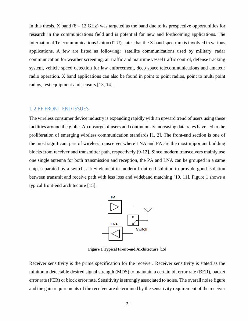
1.2 RF FRONT-END ISSUES
The wireless consumer device industry is expanding rapidly with an upward trend of users using these
facilities around the globe. An upsurge of users and continuously increasing data rates have led to the
proliferation of emerging wireless communication standards [1, 2]. The front-end section is one of
the most significant part of wireless transceiver where LNA and PA are the most important building
blocks from receiver and transmitter path, respectively [9-12]. Since modern transceivers mainly use
one single antenna for both transmission and reception, the PA and LNA can be grouped in a same
chip, separated by a switch, a key element in modern front-end solution to provide good isolation
between transmit and receive path with less loss and wideband matching [10, 11]. Figure 1 shows a
typical front-end architecture [15].
Figure 1 Typical Front-end Architecture [15]
Receiver sensitivity is the prime specification for the receiver. Receiver sensitivity is stated as the
minimum detectable desired signal strength (MDS) to maintain a certain bit error rate (BER), packet
error rate (PER) or block error rate. Sensitivity is strongly associated to noise. The overall noise figure
and the gain requirements of the receiver are determined by the sensitivity requirement of the receiver

- 3 -
[16]. The noise of the front-end receiver must be low enough to allow a weak input signal (which may
not be much stronger compared to the thermal noise floor) to be discovered/noticed. If the receiver
noise is high, the magnitude of the noise might exceed the amplitude of the weak desired signal, and
hence the signal will not be detected. Radio receivers are generally tuned to a single channel. Each
channel has a bandwidth, which determines its frequency range. Strong signals in adjacent channels
produce intermodulation (IM) signals with the weak desired signal in desired bandwidth; thus,
interfering with the desired signal [17]. The receiver should not get overwhelmed in the presence of
a strong signal in an adjacent channel while receiving a weak signal. Good filtering and high linearity
in receiver amplifiers can prevent this scenario. The theory behind IM signals and linearity will be
explained further in chapter 3.
Besides signal-to-noise ratio (SNR) of a receiver, the Error Vector Magnitude (EVM) of a transmitter
also plays a key role to ensure optimal reception. EVM is a way to measure the accuracy of
reproducing the signal vectors by the transmitter compared to the transmitted data signal from
baseband [16]. This can be seen as the signal to distortion/noise ratio in the transmitter [16]. This
necessitates transmitting as much RF signal power as possible, while pushing the noise floor as low
as it can go. However, undesired spectral components from the spurious emission and worse linearity
of the transmitter can create distortion, which will limit the maximum output power level. Hence this
can also interfere with the desired signal at the receive end. It is very challenging to keep a good
compromise between high SNR and spurious free dynamic range while maintaining desired maximum
power in transceiver design. This tradeoff between linearity, noise figure, power and spurious
emission is the key balance in transmitter and receiver design hence in front-ends [17].
LNA noise figure and gain are the most important parameters in the front-end receive path to maintain
desired SNR and linearity requirement of the receiver. On the other side, PA in transmit side of the
front-end will determine the maximum power of the transmitter maintaining the desired spurious
emissions and linearity requirement. As the front-end operation in modern wireless systems is mainly
dependent on the performance of the LNA in receive path and the PA in transmit path, in this thesis
the focus was on the design of these two circuits in the X-band. As the core of these circuits, the
transistor should be carefully selected. In this work, a 0.15µm GaN HFET design kit provided by
NRC was used [18]. Its small gate length will allow achieving a small chip size while assuring a high
power density and around 40 GHz of unity gain frequency. The unique advantages of GaN HFET in
high frequency and high power design compared to other power transistor technologies would allow
us meet the desired X band LNA/PA design requirements.

- 4 -
1.3 THESIS CONTRIBUTION
As a result of the work completed here, the following contributions have been made.
A low noise amplifier and a power amplifier have been designed for X-band operation. A new
GaN 0.15µm technology on silicon carbide wafers has been used, making use of a novel
design kit provided by NRC. To the best of our knowledge, this is the first fully integrated X
band front-end MMIC ever fabricated on a NRC GaN 0.15µm process. This process will go
to its first fabrication run. Therefore, one of the contributions of this design is to help
evaluating its capabilities at the designed frequency band. As it can provide higher power,
linearity, and robustness, it would improve front-end performance in aerospace, military, civil
communication systems and biomedical applications, as well as in the perspective of next
generation 3GPP 5G wireless communication systems [1-3, 19].
The low noise amplifier and the power amplifier designed here each occupy less than 2 mm2
die space area; the LNA has an area of 2 x 0.9 mm2 and the power amplifier occupies 2 x 0.85
mm2 of die space area in the overall front-end architecture. This occupied die area includes on
chip single supply DC bias network with RF chokes and DC blocking capacitors in the input
and output of the amplifier. Compared to available LNA and PA designs with similar figure
of merits (ex: band of interest, maximum power), it can be noted that this design is the smallest
in terms of die area. In fact, the overall front-end structure (after integrating a broadband
SPDT) could have fit into a 3 x 2 mm2 die area. However, due to foundry constraints, the only
available options were either 2 x 2 mm2 or 4 x 2 mm2. Nevertheless, even with the extra area
consumed, the final size of the front-end remains very competitive while compared to existing
designs.
1.4 THESIS ORGANIZATION
This thesis is divided as follows. After this introductory Chapter, Chapter 2 presents the front-end
architecture designed in this thesis. It also includes a brief description of material properties of GaN
highlighting the advantages of GaN in front-end design compared to similar actives devices. In
Chapter 3, low noise amplifiers and their key design parameters are reviewed, followed by widely
used wideband LNA topologies. It also includes the wideband topology designed in this thesis.
Chapter 4 details the low noise amplifier design process. The chapter also includes literature review,
the core theory behind shunt resistive feedback topology and a detailed discussion of the chosen LNA
- 5 -
architecture. Simulation results of the implemented design are also presented and successfully
compared to other works.
Chapter 5 presents the background of power amplifier. It also includes common metrics used to
evaluate PA performance. It is followed by Chapter 6, with details about the design methodology used
for the design of the X band PA. Chapter 7 presents the 10 GHz front-end design integrating the
designed X band LNA and PA along with a wideband single-pole double-throw (SPDT) switch
designed by another member of our research team. This chapter details the layout design of the front-
end architecture and its related results to ensure its performance.
Chapter 8 summarizes the research work done in this thesis and provides ideas of future research work
in this area.

- 6 -
CHAPTER 2 DESIGN CONSIDERATIONS
2.1 INTRODUCTION
In wireless systems, transceivers are comprised of transmitters and receivers to exchange information
(voice messages and data) through free space. The specifications and frequency allocation of every
class of wireless communications predetermine the topology of the system and the applicable
semiconductor technologies in the RF transceiver design. However, due to a wide range of system
requirements, each semiconductor device technology has its individual cost and performance
proposition available in different applications and bands. Gain, linearity and noise specifications are
all key parameters for all active receive chain circuits. Maximum power, linearity, power gain,
spurious emission and error vector magnitude are the key parameters for the transmit chain circuitry
[20].
2.2 FRONT-END CONFIGURATION
The front-end of a transceiver basically consists of the LNA, PA and switch and is usually
implemented using III-V semiconductor technologies such as GaAs or GaN. Usually, GaAs front-end
modules for high power telecommunication applications are comprised of circulators (Figure 2 (a)).
Such configuration occupies a large die area and also includes a limiter circuit in the receiver chain
to protect low noise amplifiers against high power inputs [10]. These components are not only costly
but also require large DC current levels, which leads to very high power consumption. In comparison
with GaAs, GaN low noise amplifiers can survive higher power up to 41 dBm [21, 22]. Therefore, a
front-end receive path can be designed requiring only a small limiter or absolutely no limiter circuit
and removing the need for expensive circulators which can be replaced by a simple wideband GaN
switch. As a result, a simple topology using a GaN PA + LNA separated by a GaN switch on a same
process can realize lighter, smaller and cheaper high power TX/RX (transmit and receive) front-end
module [15, 22, 23].
Therefore, a wideband single-pole double-throw switch (SPDT) was designed separately to be
integrated with the LNA and the PA to achieve the desired front-end configuration. GaN technology
was chosen over GaAs for all above-mentioned circuits designed in this thesis (which will be
explained in the next section). Low noise and high power devices can be fabricated side by side with
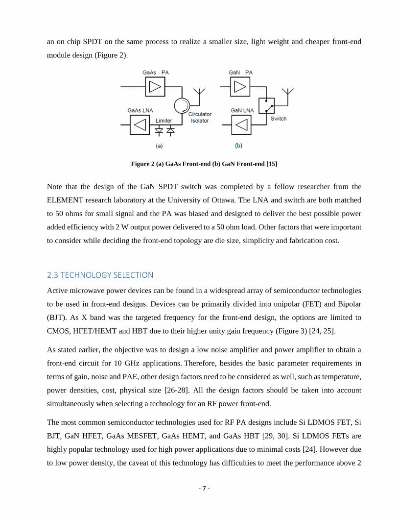
- 7 -
an on chip SPDT on the same process to realize a smaller size, light weight and cheaper front-end
module design (Figure 2).
Figure 2 (a) GaAs Front-end (b) GaN Front-end [15]
Note that the design of the GaN SPDT switch was completed by a fellow researcher from the
ELEMENT research laboratory at the University of Ottawa. The LNA and switch are both matched
to 50 ohms for small signal and the PA was biased and designed to deliver the best possible power
added efficiency with 2 W output power delivered to a 50 ohm load. Other factors that were important
to consider while deciding the front-end topology are die size, simplicity and fabrication cost.
2.3 TECHNOLOGY SELECTION
Active microwave power devices can be found in a widespread array of semiconductor technologies
to be used in front-end designs. Devices can be primarily divided into unipolar (FET) and Bipolar
(BJT). As X band was the targeted frequency for the front-end design, the options are limited to
CMOS, HFET/HEMT and HBT due to their higher unity gain frequency (Figure 3) [24, 25].
As stated earlier, the objective was to design a low noise amplifier and power amplifier to obtain a
front-end circuit for 10 GHz applications. Therefore, besides the basic parameter requirements in
terms of gain, noise and PAE, other design factors need to be considered as well, such as temperature,
power densities, cost, physical size [26-28]. All the design factors should be taken into account
simultaneously when selecting a technology for an RF power front-end.
The most common semiconductor technologies used for RF PA designs include Si LDMOS FET, Si
BJT, GaN HFET, GaAs MESFET, GaAs HEMT, and GaAs HBT [29, 30]. Si LDMOS FETs are
highly popular technology used for high power applications due to minimal costs [24]. However due
to low power density, the caveat of this technology has difficulties to meet the performance above 2
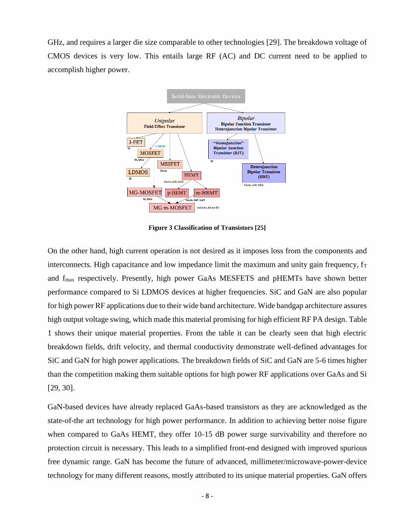
- 8 -
GHz, and requires a larger die size comparable to other technologies [29]. The breakdown voltage of
CMOS devices is very low. This entails large RF (AC) and DC current need to be applied to
accomplish higher power.
Figure 3 Classification of Transistors [25]
On the other hand, high current operation is not desired as it imposes loss from the components and
interconnects. High capacitance and low impedance limit the maximum and unity gain frequency, fT
and fmax respectively. Presently, high power GaAs MESFETS and pHEMTs have shown better
performance compared to Si LDMOS devices at higher frequencies. SiC and GaN are also popular
for high power RF applications due to their wide band architecture. Wide bandgap architecture assures
high output voltage swing, which made this material promising for high efficient RF PA design. Table
1 shows their unique material properties. From the table it can be clearly seen that high electric
breakdown fields, drift velocity, and thermal conductivity demonstrate well-defined advantages for
SiC and GaN for high power applications. The breakdown fields of SiC and GaN are 5-6 times higher
than the competition making them suitable options for high power RF applications over GaAs and Si
[29, 30].
GaN-based devices have already replaced GaAs-based transistors as they are acknowledged as the
state-of-the art technology for high power performance. In addition to achieving better noise figure
when compared to GaAs HEMT, they offer 10-15 dB power surge survivability and therefore no
protection circuit is necessary. This leads to a simplified front-end designed with improved spurious
free dynamic range. GaN has become the future of advanced, millimeter/microwave-power-device
technology for many different reasons, mostly attributed to its unique material properties. GaN offers

- 9 -
almost five times higher breakdown voltage than GaAs, allowing higher drain voltage swing [26, 29,
30].
Table 1 Material Properties of Microwave Semiconductor Devices [30]
In return, this eases the power matching and lower loss matching network, thus demonstrating higher
sheet charge and resulting in higher current densities, all leading to a reduction in the transistor area.
The other key parameter of GaN technology is high saturated drift velocity, which results in higher
saturation currents and higher power densities in GaN. This is very important for high power devices
[29-31]. Higher power density is proportionally related to a smaller die area size and would allow
simpler, low-loss power matching networks. SiC and GaN are very popular wideband technology due
to the highest power densities at 1.7 W/mm and 4.5-8W/mm, respectively [30, 31]. Conventional
GaAs FETs have much lower power densities (approximately 0.4W/mm) compared to GaN. GaN also
shows a larger band-gap in comparison to Si and GaAs (more than two times for operation in high
temperature). This means GaN can resist higher ambient and channel temperatures. Furthermore, GaN
based systems have the ability of supporting hetero-structure device technologies with a high two-
dimensional electron gas carrier density and mobility. Thus, GaN is mostly used in High-electron-
mobility-transistor (HEMT) devices, which incorporates a junction between two materials with
different bandgaps. GaN can be developed on many different substrates including Si, SiC, and
Sapphire.
Typical AlGaN devices developed on GaN have demonstrated superior current handling capabilities
[29, 30]. Since the thermal conductivity of SiC is higher than GaN, it is often the ideal preference as
a substrate to fabricate a GaN device. GaN on SiC offers high reliability and performance at large
power levels, and proves to be quite effective in design space and thermal dissipation. This is the
reason a GaN front-end using NRC GAN150 kit was selected for this work.

- 10 -
2.4 GaN LIMITATIONS
Although GaN shows clear advantages, the device technology has limitations that need to be
addressed. AlGaN/GaN HEMTS have demonstrated excellent power densities around 9.8W/mm at
8GHz [29, 30]; still significant development work is ongoing on wide bandgap technologies such as
GaN. The two main important concerns of GaN are trapping effect and thermal effects. The trapping
and thermal effect are the root cause for current collapse, drain current compression and frequency
dispersion of transconductance and capacitances [32-34]. Figure 4 shows current dispersion due to
trapping effect and thermal effect.
Figure 4 Trapping effect in GaN [35]
On the other hand, thermal and self-heating significantly affect the performance of semiconductor
devices. While the device is in high voltage and high power region, the self-heating causes electron
carriers to drift in random directions in spite of following drain to source region. Some electrons can
come out of the channel and might cause significant roll off in the high voltage high current region,
which can cause DC to RF current variations as well shown in Figure 4 [35].
Despite trapping and thermal effects, GaN still demonstrates outstanding performance for high-power
MMIC due to its material properties. It has the potential to operate up to a theoretical maximum
frequency of 155 GHz and at elevated temperatures of 700°C with SiC as the substrate [32, 36].
- 11 -
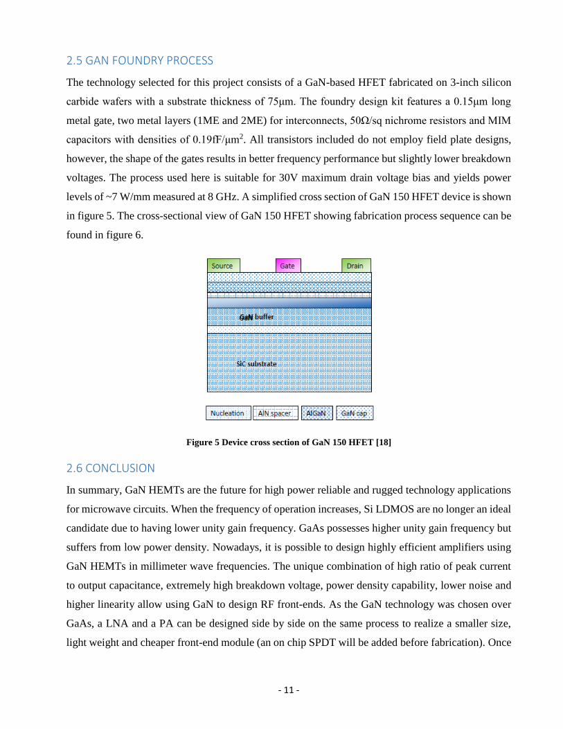
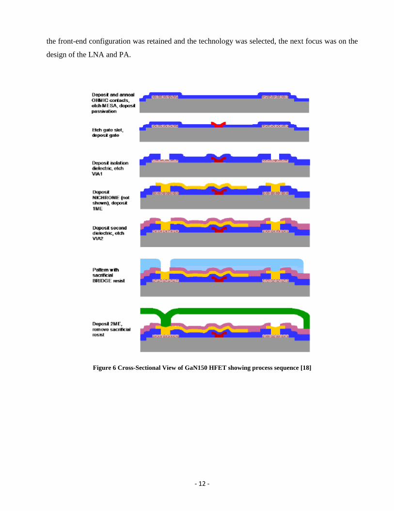
2.5 GAN FOUNDRY PROCESS
The technology selected for this project consists of a GaN-based HFET fabricated on 3-inch silicon
carbide wafers with a substrate thickness of 75μm. The foundry design kit features a 0.15μm long
metal gate, two metal layers (1ME and 2ME) for interconnects, 50Ω/sq nichrome resistors and MIM
capacitors with densities of 0.19fF/μm2. All transistors included do not employ field plate designs,
however, the shape of the gates results in better frequency performance but slightly lower breakdown
voltages. The process used here is suitable for 30V maximum drain voltage bias and yields power
levels of ~7 W/mm measured at 8 GHz. A simplified cross section of GaN 150 HFET device is shown
in figure 5. The cross-sectional view of GaN 150 HFET showing fabrication process sequence can be
found in figure 6.
Figure 5 Device cross section of GaN 150 HFET [18]
2.6 CONCLUSION
In summary, GaN HEMTs are the future for high power reliable and rugged technology applications
for microwave circuits. When the frequency of operation increases, Si LDMOS are no longer an ideal
candidate due to having lower unity gain frequency. GaAs possesses higher unity gain frequency but
suffers from low power density. Nowadays, it is possible to design highly efficient amplifiers using
GaN HEMTs in millimeter wave frequencies. The unique combination of high ratio of peak current
to output capacitance, extremely high breakdown voltage, power density capability, lower noise and
higher linearity allow using GaN to design RF front-ends. As the GaN technology was chosen over
GaAs, a LNA and a PA can be designed side by side on the same process to realize a smaller size,
light weight and cheaper front-end module (an on chip SPDT will be added before fabrication). Once
- 12 -
the front-end configuration was retained and the technology was selected, the next focus was on the
design of the LNA and PA.
Figure 6 Cross-Sectional View of GaN150 HFET showing process sequence [18]
- 13 -
CHAPTER 3 LNA DESIGN PRINCIPLES
3.1 DEFINITIONS AND KEY DESIGN PARAMETERS
Low noise amplifiers (LNAs) are one of the most fundamental design blocks in the receiver side of a
transceiver system. In typical receiver circuits, the main task of an antenna is to receive
electromagnetic waves from free space and then to convert them into electric signals. These inbound
signals can consist of both anticipated and unwanted interferer signals in frequency of interest and
neighboring cells. The task of an LNA is to provide the required amplification to the incoming signal,
which is, in most of the cases, much weaker than the unwanted interferer signal, and at the same time
to make sure the lowest amount of noise is introduced to the system so that the required signal-to-
noise (SNR) ratio is achieved. Low noise amplifier works in the linear region of a device, so linearity
is also a key specification for LNA besides gain, noise figure, and input/output matching.
By definition, signal-to-noise ratio is the ratio of desired frequency signal power Psignal versus
unwanted noise signal power Pnoise [37]. Besides noise from free space, further noise will be added
when the signal goes through a specific device. It is always desired to achieve lower noise incurred
by particular design block. The total noise FdB of an overall system is the difference between the
SNRdB (input) at the input and the SNRdB (output) at the output [16].
Due to introduced noise from the circuit, SNRdB (output) is always lower than SNRdB (input).
Receiver sensitivity, stated as the minimum detectable desired signal strength (MDS) to maintain a
certain bit error rate (BER), packet error rate (PER) or block error rate, can be expressed as [16]
Receiver Sensitivity/MDS = noise power at the antenna + SNRdB (output) + FdB (3.1)
while the total noise power at the antenna (over air) can be expressed as
PN = -174 dBm/Hz + 10 log (Bandwidth of desired signal) (3.2)
So the receiver sensitivity highly depends on the total noise figure introduced by the overall receiver.
Then, the total noise factor (Ftot) for a cascaded system can be expressed, using Frii’s equation, as:
Ftot = F1 +F2−1
G1+
F3−1
G1G2+ … … … . +
FM−1
G1….GM−1 (3.3)

- 14 -
where FN is the noise figure in dB and GN is the gain introduced by the Nth stage of the cascaded
system. From equation (3.3), it is clear that the noise figure and gain of the first stage of a cascaded
system has the most significance in the total noise figure of a receiver circuit hence in the sensitivity
of the receiver. RF front-end is the first stage the signal goes through after it is received in the antenna,
which implies, LNA noise and gain performance are very significant parameters determining receiver
sensitivity. Therefore, it is very important that the LNA introduces as little noise and as much gain as
possible while maintaining good linearity.
The other key parameter of the LNA is to offer good matching to the antenna over the frequency band
of interest. The antenna matching should assure maximum power transfer to the receiver from the
antenna. In addition, LNA needs to maintain good linearity so that an unwanted large signal cannot
saturate the radio receiver in the front-end. A large signal can also pass through LNA to the antenna
if the LNA’s reverse isolation is not sufficient [38]. Poor reverse isolation is the root cause of self-
mixing, intermodulation and DC offset in baseband. Stability is also a very important metric for both
low noise and power amplifiers.
3.2 TWO PORT S-PARAMETERS
S-parameters are generally used to characterize a multiport linear network. From figure 7, for a two-
port network, the incident (a1 and a2) and reflected (b1 and b2) waves can be stated as [37]:
b1 = S11 a1 + S12 a2; b2 = S21 a1 + S22 a2 (3.4)
Figure 7 Two-port network showing incident and reflected waves [37]

- 15 -
Therefore, the S-parameters can be defined as follows [37]:
𝑆11 =𝑅𝑒𝑓𝑙𝑒𝑐𝑡𝑒𝑑 𝑝𝑜𝑤𝑒𝑟 𝑓𝑟𝑜𝑚 𝑡ℎ𝑒 𝑛𝑒𝑡𝑤𝑜𝑟𝑘 𝑖𝑛𝑝𝑢𝑡
𝐼𝑛𝑐𝑖𝑑𝑒𝑛𝑡 𝑝𝑜𝑤𝑒𝑟 𝑎𝑡 𝑡ℎ𝑒 𝑛𝑒𝑡𝑤𝑜𝑟𝑘 𝑖𝑛𝑝𝑢𝑡 (3.5)
𝑆22 =𝑅𝑒𝑓𝑙𝑒𝑐𝑡𝑒𝑑 𝑝𝑜𝑤𝑒𝑟 𝑓𝑟𝑜𝑚 𝑡ℎ𝑒 𝑛𝑒𝑡𝑤𝑜𝑟𝑘 𝑜𝑢𝑡𝑝𝑢𝑡
𝐼𝑛𝑐𝑖𝑑𝑒𝑛𝑡 𝑝𝑜𝑤𝑒𝑟 𝑎𝑡 𝑡ℎ𝑒 𝑛𝑒𝑡𝑤𝑜𝑟𝑘 𝑜𝑢𝑡𝑝𝑢𝑡 (3.6)
𝑆21 =𝑃𝑜𝑤𝑒𝑟 𝑑𝑒𝑙𝑖𝑣𝑒𝑟𝑒𝑑 𝑡𝑜 𝑡ℎ𝑒 𝑙𝑜𝑎𝑑
𝑃𝑜𝑤𝑒𝑟 𝑎𝑣𝑎𝑖𝑙𝑎𝑏𝑙𝑒 𝑓𝑟𝑜𝑚 𝑠𝑜𝑢𝑟𝑐𝑒 (3.7)
𝑆12 =𝑅𝑒𝑓𝑙𝑒𝑐𝑡𝑒𝑑 𝑃𝑜𝑤𝑒𝑟 𝑑𝑒𝑙𝑖𝑣𝑒𝑟𝑒𝑑 𝑡𝑜 𝑡ℎ𝑒 𝑠𝑜𝑢𝑟𝑐𝑒
𝐼𝑛𝑐𝑖𝑑𝑒𝑛𝑡 𝑃𝑜𝑤𝑒𝑟 𝑜𝑛 𝑡ℎ𝑒 𝑛𝑒𝑡𝑤𝑜𝑟𝑘 𝑜𝑢𝑡𝑝𝑢𝑡 (3.8)
3.2.1 POWER MATCHING
For a circuit with source voltage VS and impedance (ZS = RS + jXS) terminated by a load impedance
(ZL = RL + j XL) with characteristic impedance of transmission line 𝑍0, the total power delivered to
the load is [37]:
𝑃𝑑𝑒𝑙𝑖𝑣𝑒𝑟𝑒𝑑 = |𝑉𝑆|2𝑅𝐿
(𝑅𝐿+𝑅𝑆)2+ (𝑋𝐿+𝑋𝑆)2 (3.9)
Solving the power delivered equation for maxima, it can be found out the maximum power can be
delivered for RL = RS and XL = - XS. The input and output reflection coefficient can be defined as
[37]:
𝛤𝐼𝑁 = 𝑏1
𝑎1= 𝑆11 +
𝑆12 𝑆21 𝛤𝐿
1− 𝑆22 𝛤𝐿 ; 𝛤𝑂𝑈𝑇 =
𝑏2
𝑎2= 𝑆22 +
𝑆12 𝑆21 𝛤𝑆
1− 𝑆11 𝛤𝑆 (3.10)
where ΓS and ΓL are the source and load reflection coefficients and can be stated as [37]:
𝛤𝑆 = 𝑍𝑆− 𝑍0
𝑍𝑆+ 𝑍𝑜 ; 𝛤𝐿 =
𝑍𝐿− 𝑍0
𝑍𝐿+ 𝑍𝑜 (3.11)
The maximum power transfer condition in terms of source and load reflection coefficients can be
stated as [37]:
𝛤𝐼𝑁 = 𝛤𝑆∗ and 𝛤𝑂𝑈𝑇 = 𝛤𝐿
∗ (3.12)
The parameters S11, the input reflection coefficient with matched load, and S22, the output reflection
coefficient with matched source are the key figure of merit for input and output power matching.

- 16 -
3.2.2 GAIN
Transducer power gain (GT), Operating power gain (GP) and available power gain (GA) are the three
most important kinds of definition for power gain available in RF amplifier theory [16] (Figure 8).
There are other definitions as well.
𝐺𝑇 = 𝑃𝐿
𝑃𝐴𝑉𝑆=
𝑃𝑜𝑤𝑒𝑟 𝑑𝑒𝑙𝑖𝑣𝑒𝑟𝑒𝑑 𝑡𝑜 𝑙𝑜𝑎𝑑
𝑃𝑜𝑤𝑒𝑟 𝑎𝑣𝑎𝑖𝑙𝑎𝑏𝑙𝑒 𝑓𝑟𝑜𝑚 𝑠𝑜𝑢𝑟𝑐𝑒 (3.13)
𝐺𝑃 = 𝑃𝐿
𝑃𝐼𝑁=
𝑃𝑜𝑤𝑒𝑟 𝑑𝑒𝑙𝑖𝑣𝑒𝑟𝑒𝑑 𝑡𝑜 𝑙𝑜𝑎𝑑
𝑃𝑜𝑤𝑒𝑟 𝑖𝑛𝑝𝑢𝑡 𝑡𝑜 𝑡ℎ𝑒 𝑛𝑒𝑡𝑤𝑜𝑟𝑘 (3.14)
𝐺𝐴 = 𝑃𝐴𝑉𝑁
𝑃𝐴𝑉𝑆=
𝑃𝑜𝑤𝑒𝑟 𝑎𝑣𝑎𝑖𝑙𝑎𝑏𝑙𝑒 𝑓𝑟𝑜𝑚 𝑡ℎ𝑒 𝑛𝑒𝑡𝑤𝑜𝑟𝑘
𝑃𝑜𝑤𝑒𝑟 𝑎𝑣𝑎𝑖𝑙𝑎𝑏𝑙𝑒 𝑓𝑟𝑜𝑚 𝑠𝑜𝑢𝑟𝑐𝑒 (3.15)
Figure 8 Typical 1 stage amplifier with input and output matching network [37]
3.3 NOISE
Noise is, by definition, an unwanted signal generated internally in the channel which degrades the
desired signal response. The degradation of desired signal response can be formed as fluctuations in
signal amplitude magnitude, phase and spectral content. The main types of noise are thermal, flicker
and shot noise. Thermal noise is generated due to the heat in the electrical devices, which energizes
electron carriers and fluctuate their movement. Both gate and drain channel noise are influenced by
thermal noise [16, 38]. Although GaN HEMTs are popular for high frequency operation, flicker or
1/f noise is very important to characterize for switching application for this device. As GaN HEMT
is used for high bias voltage application, further attention is given to characterize noise for
AlGaN/GaN HEMTs under high bias voltage and current. Studies show that the noise factor increases
slowly with increasing drain voltage but decreases with high drain current [39-41].

- 17 -
There are four important sources of noise in AlGaN/GaN HEMTs. The first primary reason is the
scattering of channel electrons due to the fluctuation in velocity. This is due to the heterojunction
interface with impurities and lattice (phonon). Secondly, gate voltage fluctuations are highly
correlated with drain current variations in channel, which also creates noise in GaN HEMT structure.
Both first and second reasons are frequency independent. The third reason is that electrons randomly
get injected into the channel due to gate leakage, which results in shot noise [39-41]. The fourth source
of noise is electron trapping which was explained in details in earlier section.
In RF system, noise factor (F) is the metric for noise. Noise figure (NF) is noise factor expressed in
decibels [16]:
𝐹 = 𝑆𝑁𝑅 𝑎𝑡 𝑡ℎ𝑒 𝑖𝑛𝑝𝑢𝑡
𝑆𝑁𝑅 𝑎𝑡 𝑡ℎ𝑒 𝑜𝑢𝑡𝑝𝑢𝑡 (3.16)
NF = 10log (F) (3.17)
3.4 STABILITY
Stability is one of the key performance metrics for amplifiers. The amplifier becomes unstable due to
spurious oscillation. Spurious oscillations are mainly due to feedback and gain. A common design
goal is to make sure the amplifier can maintain stability with a larger gain for a wider bandwidth
making sure all the conducted and the radiated feedback paths are adequately attenuated [16]. Even
if there is no evident oscillation from the amplifier, the frequency of oscillation can be low enough
and it is very hard to measure because the oscillation signal might have been mitigated extensively
by DC blocking capacitors. The conditions for unconditional stability is given by the Rollett’s stability
factor (K factor):
𝐾 = 1− |𝑆21|2−|𝑆22|2+|𝛥|2
2.|𝑆12.𝑆21| > 1 (3.18)
|𝛥| = | 𝑆11. 𝑆22 − 𝑆12 𝑆21| < 1 (3.19)
𝐵 = 1 + |𝑆11|2 − |𝑆22|2 − |𝛥|2 > 0 (3.20)

- 18 -
As seen from the above equations, the stability factor (K) and the stability measure (B) are expressed
using S – parameters. Stability factor K and stability measure B needs to be respectively greater than
1 and 0 consecutively over a frequency of range where the amplifier has gain to achieve unconditional
stability. However, failing unconditional stability does not imply that the circuit is unstable.
3.5 LINEARITY OVERVIEW
In a linear system, the output is linearly related to the input. Nonlinearities are created mainly due to
active elements in the circuit or the signal swing being limited by the power supply rails. The primary
figures to measure nonlinearity of an amplifier are 1 dB compression point (P1dB) or at saturation
(PSAT), and inter-modulation distortion and intercept points [16].
3.5.1 1- dB COMPRESSION POINT
The output referred 1-dB compression point is the output level of an amplifier when the linear gain is
reduced by exactly 1 dB. At this point, the amplifier saturates and the output power does not increase
much with the increase of input power. The output power level where the amplifier is saturated is
known as Psat. In large signal, when the power level is higher, the amplifier gain is reduced and the
amplifier enters into gain compression (Figure 9). The output referred 1-dB compression point can be
expressed as [16]:
OP1dB = IP1dB + (G -1) [dB] (3.21)
where G is the linear gain of the amplifier.

- 19 -
Figure 9 1-dB compression point, IIP3 & IIP2 [16]
3.5.2 HARMONICS, IMD AND INTERCEPT POINT
Intermodulation distortion (IMD) products are basically the sum and difference of fundamental input
signals and their associated harmonics when multiple signals are at the input of the amplifier. IMD
products are more problematic to deal with than harmonic distortion, because IMD products,
especially the third order IMD product, can be close to the desired signal and thus harder to filter out
than harmonics. Like third order, any lower frequency second order harmonics product can increase
nonlinearity and decrease efficiency by interfering with DC bias of the transistor. To explain
harmonics and inter modulation distortion products, figure 10 is presented with two fundamental
frequencies f1 and f2 at the input of the system while IMD components get created at the output of
the amplifier.
Figure 10 Fundamental and IMD tones [16]
- 20 -
The odd order intermodulation products (2f1 – f2, 2f2 – f1, 3f1 – 2f2, 3f2 – 2f1) are close to the two
fundamental tone frequencies f1 and f2. The magnitude of Intermodulation distortion can be stated as
[16]:
IMD (dBc) = POUT1dB – POUTIMD (3.22)
POUTIMD is the output power of third order intermodulation product. The magnitude of IMD product
can increase with the carrier spacing. As shown in figure 10, the second order intercept point (IIP2)
slope of the linear extension of 2f1, 2f2, f1-f2 and f1+f2 tones intersects with linear extension of
fundamental slope. Third order intercept point (IIP3) is the point where the linear extension of the
slope of 3f1, 3f2, 2f1-f2 and 2f2-f1 IMD tones intersects with the fundamental slope [16]. IIP3, IIP2
and 1-dB compression points are the most important figures of merit of linearity of an amplifier, both
LNA and PA.
3.6 POPULAR WIDEBAND LNA TOPOLOGIES
As discussed earlier the most important parameters of LNA design are small signal gain, noise figure
and input/output matching. In general, LNA topologies are differentiated depending on their matching
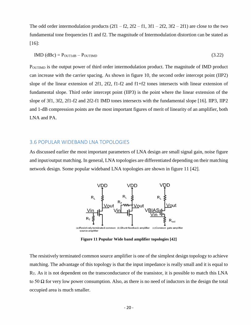
network design. Some popular wideband LNA topologies are shown in figure 11 [42].
Figure 11 Popular Wide band amplifier topologies [42]
The resistively terminated common source amplifier is one of the simplest design topology to achieve
matching. The advantage of this topology is that the input impedance is really small and it is equal to
RT. As it is not dependent on the transconductance of the transistor, it is possible to match this LNA
to 50 Ω for very low power consumption. Also, as there is no need of inductors in the design the total
occupied area is much smaller.
- 21 -
The disadvantages of this topology are lower gain and higher noise figure. The noise figure is worse
due to the matching resistor. The minimum noise figure attained by this structure is 6 dB. Due to the
resistor, the signal is attenuated at the input. Therefore the linearity is better but the gain achieved is
lower [42].
In the common gate configuration, the signal is fed into the source of a transistor. The input impedance
of a common gate topology is inversely proportional to the transconductance gm of the transistor.
Therefore, the downside is high power consumption to match to 50 Ω [42].
The configuration investigated in this thesis corresponds to the shunt resistive feedback amplifier.
The input impedance of this topology is realized by the Miller theorem. That is dividing feedback
resistor RF by the gain of the LNA [42]. The input impedance and approximate noise factor of the
topology is stated below [42]:
𝑍𝑖𝑛 = 𝑅𝐹
1+(𝑔𝑚 − 1
𝑅𝐹)( 𝑅𝐹 ||𝑅𝐿 ||𝑟𝑜)
(3.23)
𝐹 = 1 + 𝑅𝑆
𝑅𝐹 (3.24)
From the equations above, choosing high feedback resistor will not only achieve broadband matching
but also will lower the noise figure.
3.7 CONCLUSION
As previously stated in our introductory chapter, one of the goals of this thesis is to design a low noise
amplifier for X band to achieve an overall design for 10 GHz RF front-end module. Parallel resistive
feedback topology was chosen over series feedback and common gate topology to realize the LNA
design for the RF front-end. The main advantage of this topology is the overall gain flatness. The
shunt feedback resistor can provide higher bandwidth for input/output matching which can also lower
the noise figure compared to other two wideband topologies. This topology can also reduce the I/O
VSWRs and is also immune to device intrinsic parameters, (further explained in section 4.3.1) which
ensures the robustness of the design.
- 22 -
CHAPTER 4 LOW NOISE AMPLIFIER DESIGN
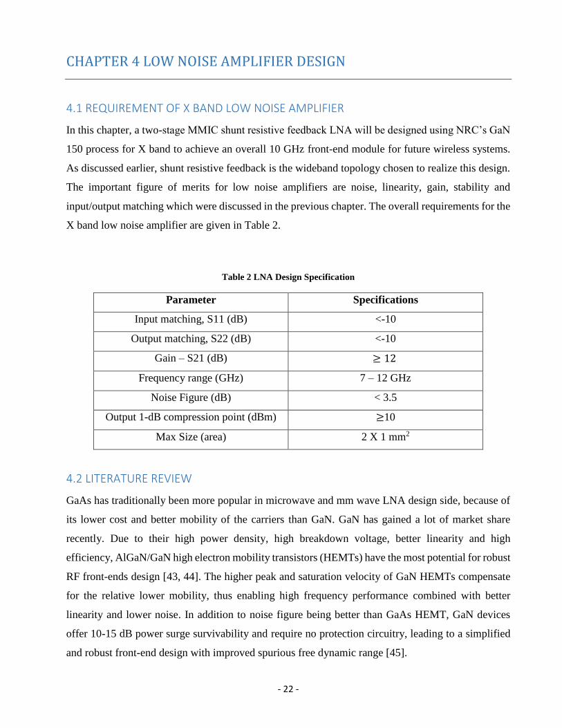
4.1 REQUIREMENT OF X BAND LOW NOISE AMPLIFIER
In this chapter, a two-stage MMIC shunt resistive feedback LNA will be designed using NRC’s GaN
150 process for X band to achieve an overall 10 GHz front-end module for future wireless systems.
As discussed earlier, shunt resistive feedback is the wideband topology chosen to realize this design.
The important figure of merits for low noise amplifiers are noise, linearity, gain, stability and
input/output matching which were discussed in the previous chapter. The overall requirements for the
X band low noise amplifier are given in Table 2.
Table 2 LNA Design Specification
Parameter Specifications
Input matching, S11 (dB) <-10
Output matching, S22 (dB) <-10
Gain – S21 (dB) ≥ 12
Frequency range (GHz) 7 – 12 GHz
Noise Figure (dB) < 3.5
Output 1-dB compression point (dBm) ≥10
Max Size (area) 2 X 1 mm2
4.2 LITERATURE REVIEW
GaAs has traditionally been more popular in microwave and mm wave LNA design side, because of
its lower cost and better mobility of the carriers than GaN. GaN has gained a lot of market share
recently. Due to their high power density, high breakdown voltage, better linearity and high
efficiency, AlGaN/GaN high electron mobility transistors (HEMTs) have the most potential for robust
RF front-ends design [43, 44]. The higher peak and saturation velocity of GaN HEMTs compensate
for the relative lower mobility, thus enabling high frequency performance combined with better
linearity and lower noise. In addition to noise figure being better than GaAs HEMT, GaN devices
offer 10-15 dB power surge survivability and require no protection circuitry, leading to a simplified
and robust front-end design with improved spurious free dynamic range [45].
- 23 -
There has been an extensive effort on applying wideband amplification techniques in GaN X band
LNA designs to achieve a smaller, lower cost, low noise and robust front-end design. In [10], a RF
receiver front-end was designed by M. Thorsell et al for X band on a unique structure of GaN
consisting of a 25 nm Al0.25Ga0.75N layer on top of a 2 µm undopped GaN buffer on semi-insulating
SiC. In [10], a two-stage low noise amplifier was implemented using inductive feedback and resistive
feedback in the first and second stage, respectively. After fabrication, the LNA experienced a
degradation in the input matching due to the spiral inductor value used in the first stage to design
inductive feedback topology. In [11], S. Masuda et al claimed that his design corresponded to the first
X band GaN front-end MMIC ever reported. The MMIC was fabricated using 0.25 µm AlGaN/GaN
HEMT technology and featured a two-stage LNA using microstrip matching and shunt RC bias
network to achieve input/output matching with unconditional stability. In [46], three X band robust
low noise amplifiers were designed by A. Bettidi et al, using a multi-stage amplification topology
with two different bias condition (15% and 20 % of saturated current). In [46] the design goal was to
achieve 2.5 dB noise figure for 8-11 GHz range with associated gain of 20 dB and overdrive power
survivability of more than 38 dBm. Experimental data for [46] showed the best performance with
respect to gain, noise figure and power consumption can be achieved for 15 % of saturated current,
which is very similar to GaAs [46]. In [46] the designed LNAs showed a similar gain and noise figure
response for both 15 % and 20% of saturated current conditions. In [47], a low noise amplifier was
designed by Ulrich et al using a 0.25 µm GaN-HEMT process. The designed LNA in [47] exhibited
25 dBm of output power and 28 dBm of OIP3 at 8 GHz, which was 8 dB higher than output referred
1 dB compression point. The proposed design in this chapter will be compared with existing X band
low noise amplifier work available in the literature [46-50] as well as with other commercial X band
low noise amplifiers (GaN and 0.15 µm 3MI PHEMT from Triquint Technology) [51-53].
An LNA can be designed in several ways. It can be either realized using single-ended or differential
topologies. It can also be designed either using single-stage or multi-stage configurations, accounting
for several different tradeoffs. The biggest shortcoming of a single-ended LNA architecture is its
sensitivity to parasitic ground inductance, which is also prone to low frequency supply noise. A
differential LNA can solve this issue. But for equal total power consumption, the noise figure of
differential LNA is higher than its single-ended counterpart [54]. Higher gain can be achieved through
multi-stage design but it is more difficult to handle its stability than single-ended one Final design
values and DC bias conditions are dependent on the application and specific design requirements. The
goal of this design was to realize a wide band low noise amplifier for X band. The approach described
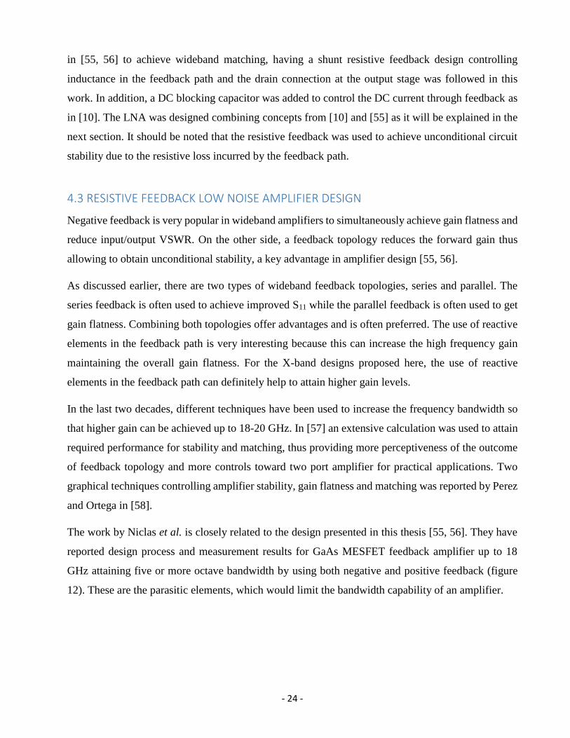
- 24 -
in [55, 56] to achieve wideband matching, having a shunt resistive feedback design controlling
inductance in the feedback path and the drain connection at the output stage was followed in this
work. In addition, a DC blocking capacitor was added to control the DC current through feedback as
in [10]. The LNA was designed combining concepts from [10] and [55] as it will be explained in the
next section. It should be noted that the resistive feedback was used to achieve unconditional circuit
stability due to the resistive loss incurred by the feedback path.
4.3 RESISTIVE FEEDBACK LOW NOISE AMPLIFIER DESIGN
Negative feedback is very popular in wideband amplifiers to simultaneously achieve gain flatness and
reduce input/output VSWR. On the other side, a feedback topology reduces the forward gain thus
allowing to obtain unconditional stability, a key advantage in amplifier design [55, 56].
As discussed earlier, there are two types of wideband feedback topologies, series and parallel. The
series feedback is often used to achieve improved S11 while the parallel feedback is often used to get
gain flatness. Combining both topologies offer advantages and is often preferred. The use of reactive
elements in the feedback path is very interesting because this can increase the high frequency gain
maintaining the overall gain flatness. For the X-band designs proposed here, the use of reactive
elements in the feedback path can definitely help to attain higher gain levels.
In the last two decades, different techniques have been used to increase the frequency bandwidth so
that higher gain can be achieved up to 18-20 GHz. In [57] an extensive calculation was used to attain
required performance for stability and matching, thus providing more perceptiveness of the outcome
of feedback topology and more controls toward two port amplifier for practical applications. Two
graphical techniques controlling amplifier stability, gain flatness and matching was reported by Perez
and Ortega in [58].
The work by Niclas et al. is closely related to the design presented in this thesis [55, 56]. They have
reported design process and measurement results for GaAs MESFET feedback amplifier up to 18
GHz attaining five or more octave bandwidth by using both negative and positive feedback (figure
12). These are the parasitic elements, which would limit the bandwidth capability of an amplifier.
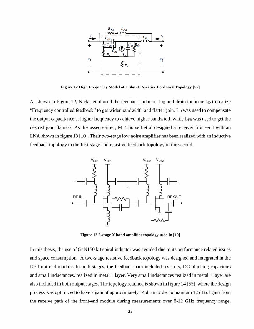
- 25 -
Figure 12 High Frequency Model of a Shunt Resistive Feedback Topology [55]
As shown in Figure 12, Niclas et al used the feedback inductor LFB and drain inductor LD to realize
“Frequency controlled feedback” to get wider bandwidth and flatter gain. LD was used to compensate
the output capacitance at higher frequency to achieve higher bandwidth while LFB was used to get the
desired gain flatness. As discussed earlier, M. Thorsell et al designed a receiver front-end with an
LNA shown in figure 13 [10]. Their two-stage low noise amplifier has been realized with an inductive
feedback topology in the first stage and resistive feedback topology in the second.
Figure 13 2-stage X band amplifier topology used in [10]
In this thesis, the use of GaN150 kit spiral inductor was avoided due to its performance related issues
and space consumption. A two-stage resistive feedback topology was designed and integrated in the
RF front-end module. In both stages, the feedback path included resistors, DC blocking capacitors
and small inductances, realized in metal 1 layer. Very small inductances realized in metal 1 layer are
also included in both output stages. The topology retained is shown in figure 14 [55], where the design
process was optimized to have a gain of approximately 14 dB in order to maintain 12 dB of gain from
the receive path of the front-end module during measurements over 8-12 GHz frequency range.
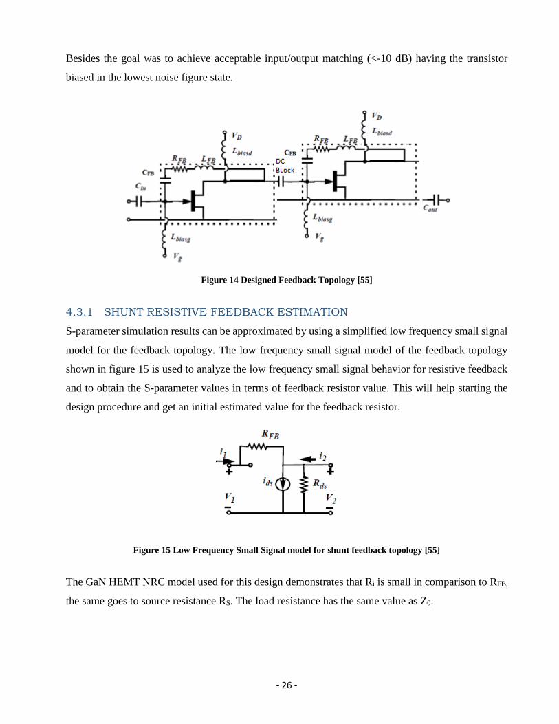
- 26 -
Besides the goal was to achieve acceptable input/output matching (<-10 dB) having the transistor
biased in the lowest noise figure state.
Figure 14 Designed Feedback Topology [55]
4.3.1 SHUNT RESISTIVE FEEDBACK ESTIMATION
S-parameter simulation results can be approximated by using a simplified low frequency small signal
model for the feedback topology. The low frequency small signal model of the feedback topology
shown in figure 15 is used to analyze the low frequency small signal behavior for resistive feedback
and to obtain the S-parameter values in terms of feedback resistor value. This will help starting the
design procedure and get an initial estimated value for the feedback resistor.
Figure 15 Low Frequency Small Signal model for shunt feedback topology [55]
The GaN HEMT NRC model used for this design demonstrates that Ri is small in comparison to RFB,
the same goes to source resistance RS. The load resistance has the same value as Z0.

- 27 -
The relationship between current and voltages can be expressed in terms of admittance matrix [55]:
[𝐼1
𝐼2] = [
1
𝑅𝐹𝐵
−1
𝑅𝐹𝐵
𝑔𝑚 −1
𝑅𝐹𝐵
1
𝑅𝐹𝐵+ 𝐺𝑑𝑠
] [𝑉1
𝑉2] (4.1)
with:
𝑉𝑔𝑠 = 𝑉1; 𝐼𝑑𝑠 = 𝑔𝑚 𝑉𝑔𝑠; 𝐺𝑑𝑠 = 𝑅𝑑𝑠−1 (4.2)
The S-parameters can be derived as [55]:
𝑆11 = 1
𝛴[
𝑅𝐹𝐵
𝑍0 (1 + 𝐺𝑑𝑠𝑍𝑜 ) − (𝑔𝑚 + 𝐺𝑑𝑠 )𝑍𝑜)] (4.3)
𝑆12 = 2
𝛴 (4.4)
𝑆21 = −2
𝛴 [ 𝑔𝑚𝑅𝐹𝐵 − 1] (4.5)
𝑆22 = 1
𝛴[
𝑅𝐹𝐵
𝑍0 (1 − 𝐺𝑑𝑠𝑍𝑜 ) − (𝑔𝑚 + 𝐺𝑑𝑠 )𝑍𝑜)] (4.6)
with:
𝛴 = 𝑅𝐹𝐵
𝑍0 (1 + 𝐺𝑑𝑠𝑍𝑜 ) + (𝑔𝑚 + 𝐺𝑑𝑠 )𝑍𝑜 + 2 (4.7)
From equation (4.3), (4.6) and (4.7) simultaneous input/output matching (S11 = S22 = 0) can only be
satisfied for 𝐺𝑑𝑠 = 0 and 𝑅𝐹𝐵
𝑍0= 𝑔𝑚𝑍𝑜 [55]. From [55], we get:
𝑆11 = 0 (4.8)
𝑆22 = 0 (4.9)
𝑆12 = 1
𝑔𝑚𝑍𝑜+1 (4.10)
𝑆21 = −(𝑔𝑚𝑍0 − 1) = −( 𝑅𝐹𝐵
𝑍𝑜− 1) (4.11)
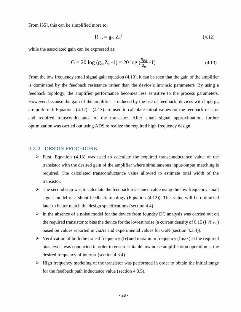
- 28 -
From [55], this can be simplified more to:
RFB = gm Zo2 (4.12)
while the associated gain can be expressed as:
G = 20 log (gm Zo -1) = 20 log (𝑅𝐹𝐵
𝑍0 -1) (4.13)
From the low frequency small signal gain equation (4.13), it can be seen that the gain of the amplifier
is dominated by the feedback resistance rather than the device’s intrinsic parameters. By using a
feedback topology, the amplifier performance becomes less sensitive to the process parameters.
However, because the gain of the amplifier is reduced by the use of feedback, devices with high gm
are preferred. Equations (4.12) – (4.13) are used to calculate initial values for the feedback resistor
and required transconductance of the transistor. After small signal approximation, further
optimization was carried out using ADS to realize the required high frequency design.
4.3.2 DESIGN PROCEDURE
First, Equation (4.13) was used to calculate the required transconductance value of the
transistor with the desired gain of the amplifier where simultaneous input/output matching is
required. The calculated transconductance value allowed to estimate total width of the
transistor.
The second step was to calculate the feedback resistance value using the low frequency small
signal model of a shunt feedback topology (Equation (4.12)). This value will be optimized
later to better match the design specifications (section 4.4).
In the absence of a noise model for the device from foundry DC analysis was carried out on
the required transistor to bias the device for the lowest noise (a current density of 0.15 (ID/IDSS)
based on values reported in GaAs and experimental values for GaN (section 4.3.4)).
Verification of both the transit frequency (fT) and maximum frequency (fmax) at the required
bias levels was conducted in order to ensure suitable low noise amplification operation at the
desired frequency of interest (section 4.3.4).
High frequency modeling of the transistor was performed in order to obtain the initial range
for the feedback path inductance value (section 4.3.5).
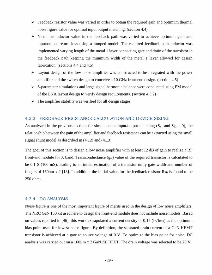
- 29 -
Feedback resistor value was varied in order to obtain the required gain and optimum thermal
noise figure value for optimal input output matching. (section 4.4)
Next, the inductor value in the feedback path was varied to achieve optimum gain and
input/output return loss using a lumped model. The required feedback path inductor was
implemented varying length of the metal 1 layer connecting gate and drain of the transistor in
the feedback path keeping the minimum width of the metal 1 layer allowed for design
fabrication. (sections 4.4 and 4.5)
Layout design of the low noise amplifier was constructed to be integrated with the power
amplifier and the switch design to conceive a 10 GHz front-end design. (section 4.5)
S-parameter simulations and large signal harmonic balance were conducted using EM model
of the LNA layout design to verify design requirements. (section 4.5.2)
The amplifier stability was verified for all design stages.
4.3.3 FEEDBACK RESISTANCE CALCULATION AND DEVICE SIZING
As analyzed in the previous section, for simultaneous input/output matching (S11 and S22 = 0), the
relationship between the gain of the amplifier and feedback resistance can be extracted using the small
signal shunt model as described in (4.12) and (4.13).
The goal of this section is to design a low noise amplifier with at least 12 dB of gain to realize a RF
front-end module for X band. Transconductance (gm) value of the required transistor is calculated to
be 0.1 S (100 mS), leading to an initial estimation of a transistor unity gate width and number of
fingers of 160um x 2 [18]. In addition, the initial value for the feedback resistor RFB is found to be
250 ohms.
4.3.4 DC ANALYSIS
Noise figure is one of the most important figure of merits used in the design of low noise amplifiers.
The NRC GaN 150 kit used here to design the front-end module does not include noise models. Based
on values reported in [46], this work extrapolated a current density of 0.15 (ID/IDSS) as the optimum
bias point used for lowest noise figure. By definition, the saturated drain current of a GaN HEMT
transistor is achieved at a gate to source voltage of 0 V. To optimize the bias point for noise, DC
analysis was carried out on a 160µm x 2 GaN150 HFET. The drain voltage was selected to be 20 V.
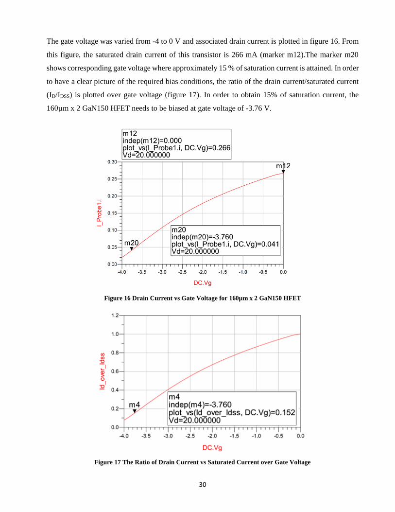
- 30 -
The gate voltage was varied from -4 to 0 V and associated drain current is plotted in figure 16. From
this figure, the saturated drain current of this transistor is 266 mA (marker m12).The marker m20
shows corresponding gate voltage where approximately 15 % of saturation current is attained. In order
to have a clear picture of the required bias conditions, the ratio of the drain current/saturated current
(ID/IDSS) is plotted over gate voltage (figure 17). In order to obtain 15% of saturation current, the
160µm x 2 GaN150 HFET needs to be biased at gate voltage of -3.76 V.
Figure 16 Drain Current vs Gate Voltage for 160µm x 2 GaN150 HFET
Figure 17 The Ratio of Drain Current vs Saturated Current over Gate Voltage
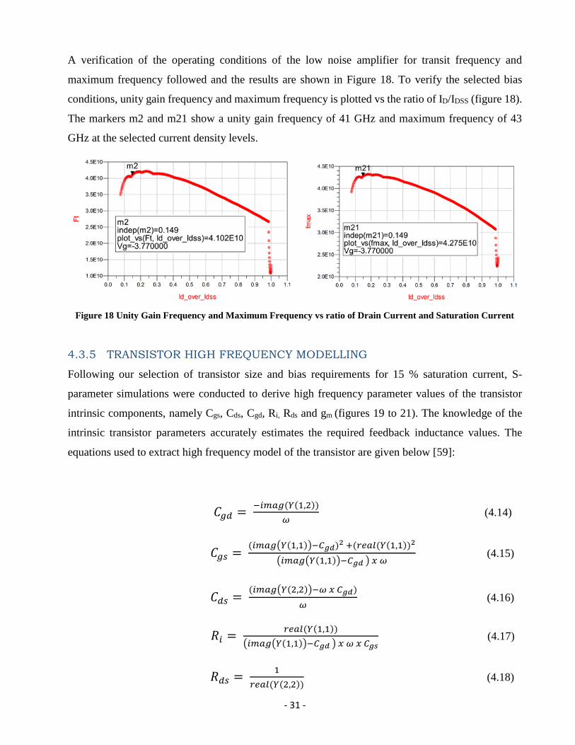
- 31 -
A verification of the operating conditions of the low noise amplifier for transit frequency and
maximum frequency followed and the results are shown in Figure 18. To verify the selected bias
conditions, unity gain frequency and maximum frequency is plotted vs the ratio of ID/IDSS (figure 18).
The markers m2 and m21 show a unity gain frequency of 41 GHz and maximum frequency of 43
GHz at the selected current density levels.
Figure 18 Unity Gain Frequency and Maximum Frequency vs ratio of Drain Current and Saturation Current
4.3.5 TRANSISTOR HIGH FREQUENCY MODELLING
Following our selection of transistor size and bias requirements for 15 % saturation current, S-
parameter simulations were conducted to derive high frequency parameter values of the transistor
intrinsic components, namely Cgs, Cds, Cgd, Ri, Rds and gm (figures 19 to 21). The knowledge of the
intrinsic transistor parameters accurately estimates the required feedback inductance values. The
equations used to extract high frequency model of the transistor are given below [59]:
𝐶𝑔𝑑 = −𝑖𝑚𝑎𝑔(𝑌(1,2))
𝜔 (4.14)
𝐶𝑔𝑠 = (𝑖𝑚𝑎𝑔(𝑌(1,1))−𝐶𝑔𝑑)2
+(𝑟𝑒𝑎𝑙(𝑌(1,1))2
(𝑖𝑚𝑎𝑔(𝑌(1,1))−𝐶𝑔𝑑 ) 𝑥 𝜔 (4.15)
𝐶𝑑𝑠 = (𝑖𝑚𝑎𝑔(𝑌(2,2))−𝜔 𝑥 𝐶𝑔𝑑)
𝜔 (4.16)
𝑅𝑖 = 𝑟𝑒𝑎𝑙(𝑌(1,1))
(𝑖𝑚𝑎𝑔(𝑌(1,1))−𝐶𝑔𝑑 ) 𝑥 𝜔 𝑥 𝐶𝑔𝑠 (4.17)
𝑅𝑑𝑠 = 1
𝑟𝑒𝑎𝑙(𝑌(2,2)) (4.18)

- 32 -
𝑔𝑚 = 𝜕𝐼𝑑
𝜕𝑉𝑔𝑠 (4.19)
Figure 19 Transconductance of 160µm x 2 GaN150 HFET @ 15% Saturation Current Bias Point vs frequency
Figure 20 Gate to Drain and Drain to Source Capacitance vs frequency

- 33 -
Figure 21 Drain to Source & Input resistance & Gate to Source Capacitance vs frequency
The high frequency parameter values of required GaN FET achieved from figures 19 – 21 are shown
in Table 3. The required bias voltage for 15 % saturation current was provided while extracting this
parameter values. These values are close to the parameter values reported in [55, 56, 10].
Table 3 HIGH FREQUENCY PARAMETERS OF 160µm x 2 GaN150 HFET
gm ≈ 0.1 S (1 GHz – 20 GHz)
Cgd 52 fF to 47 fF (1 GHz – 20 GHz)
Cds 26.2 fF to 25.8 fF (1 GHz – 20 GHz)
Cgs ≈ 0.32 pF (1 GHz – 20 GHz)
Ri 3 Ω to 9 Ω (1 GHz – 20 GHz)
Rds 217 Ω to 413 Ω (1 GHz – 20 GHz)
Also based on literature, the inductance in the feedback path will be varied from 0.1 – 1 nH in order
to achieve optimum gain and input/output return loss using a lumped inductor component. The final
optimized value of the inductor in the feedback path will be designed in section 4.5 (layout design)
Section 4.4 will also demonstrate the feedback inductance value (realized by metal 1 layer) in
schematic level.
- 34 -
4.4 SCHEMATIC DESIGN AND RESULT
The goal of this section is to realize a two-stage shunt feedback amplifier that can meet the design
specifications (Figure 22). From section 4.3.3, the initial value of the feedback path resistor was
calculated to be 250 Ω. A DC blocking capacitor of 1 pF was added to control the DC current through
feedback path as in [10]. Following our selection of transistor size, bias requirements for 15 %
saturation current and high frequency characterization of the required transistor, S-parameter
simulations were conducted varying the feedback resistor value from 150 Ω to 300 Ω using lumped
resistor component. In a feedback path, there is always a tradeoff between gain, VSWR and noise.
Figure 23(a) demonstrates that the gain of the amplifier increases with the increasing value of the
feedback path resistor, while figure 24 shows the correlation between feedback path resistor value
and the noise figure of the circuit which takes into account only thermal noise no channel noise, flicker
noise or shot noise as the noise model wasn’t available from the foundry. From this figure, it can be
concluded that although the shunt resistor in the feedback path is the biggest contributor for noise, the
overall noise figure of the amplifier decreases with the increasing value of the feedback path resistor,
as expected based on eq. (3.24).
From figures 23 and 24, it can be seen that the maximum gain and lowest noise figure can be attained
when a feedback resistor value of 300 Ω is used, but resulting in a degradation of the input matching.
The output return loss was found to be better than 20 dB for the entire range of the resistor values.
However RFB = 230 Ω provided the best match for output at 10 GHz, which also offered adequate
gain, input matching and good noise figure. GaN150 kit nicrome resistor was used to implement
feedback path resistor of 230 Ω. The minimum width of GaN kit nicrome resistor is 5 µm, which was
used in our design to realize the resistance value. The length of the resistor was varied from 10 µm to
30 µm to obtain the required feedback resistance of 230 Ω. Figure 25 demonstrates that 230 Ω can be
achieved from 5 µm wide and 23 µm long nicrome resistor from GaN150 NRC kit.
Careful design requires both schematic and layout views to be adjusted often and simultaneously.
The design tool used here allowed for EM co-simulation thus simplifying design iteration but most
importantly reducing the chances for human errors due to translating from one design environment to
another. The layout design section (4.5) will cover the layout details and the EM Co-Simulation results
to incorporate EM model discrepancies.
Figure 26 shows the overall layout driven schematic for the low noise amplifier. First the DC bias
voltage was chosen to odtain 15% of saturation drain current in section 4.2.4 (optimized bias condition

- 35 -
for noise). In the beginning of this section the required value for RFB (feedback path resistor) and
capacitor in the feedback path were selected to be 230 Ω and 1pF.
Figure 22 Basic Schematic of 2 stage Shunt Feedback Amplifier
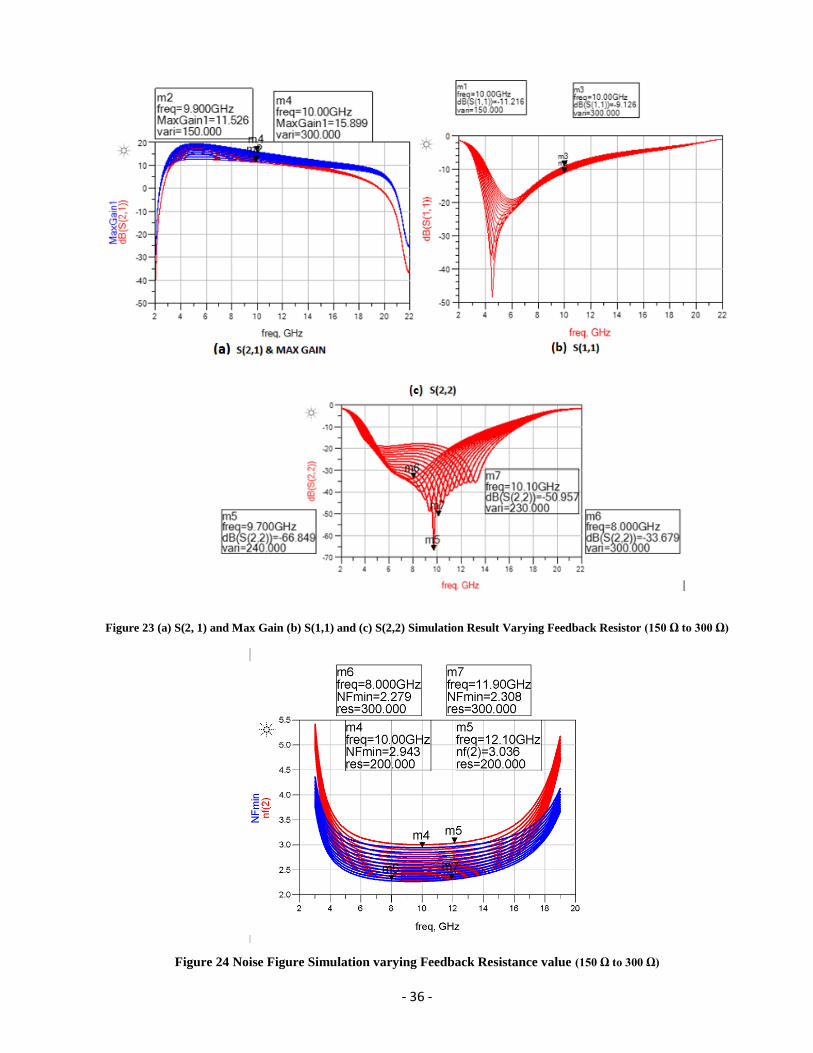
- 36 -
Figure 23 (a) S(2, 1) and Max Gain (b) S(1,1) and (c) S(2,2) Simulation Result Varying Feedback Resistor (150 Ω to 300 Ω)
Figure 24 Noise Figure Simulation varying Feedback Resistance value (150 Ω to 300 Ω)

- 37 -
Figure 25 Characterization of GaN Kit Nicrome Resistor
Next, the inductance in the Feedback path was varied in order to achieve optimum gain and
input/output return loss. The feedback inductor value was varied from 0.1 to 1 nH using lumped
inductor component from ADS. Figures 27 to 29 show the gain and input/output matching varying
lumped inductor value in the feedback path. They highlight that the minimum output return loss was
achieved for 0.1 nH at 10 GHz while an inductance value of 0.5 nH provided the maximum gain with
adequate input/output return loss. Therefore, a 0.5nH inductor was designed in the layout design
section to be used in the feedback path (4.5). During the schematic design process, a correlation
between the output return loss and drain inductance value was observed. Degradation of the output
return loss was observed for longer metal 1 connection from the drain of the transistor to the output
stage of the amplifier. Metal 1 layer connection can be characterized as inductors and the inductance
value realized by metal 1 connection goes higher with its increasing length. To characterize this
behavior a range of very small inductance value (0.01 nH to 0.02 nH) was varied using a lumped
component at the output of the amplifier connecting the drain of the device. Figures 30 and 31 show
gain and input/output return loss of the amplifier as a result of this variation. From figures 30 and 31,
the best gain was achieved for 0.05 nH and the best input and output matching were realized for 0.03
nH and 0.010 nH of drain inductance. Also, the change in drain inductance has very little effect on
gain and input return loss. However it has the most effect on the output matching of the amplifier.
Therefore, the decision was made not to design it separately but to realize the smallest possible metal
1 layer design to connect the drain of the transistor to the output stage. Finally, figures 32 and 33
show the inductance value realized by the metal 1 layer in feedback path and connecting the drain of
the transistor and the output stage of the amplifier in schematic level. Figures 32 and 33 also show
corresponding resistance values from the metal 1 connection in schematic level.

- 38 -
Figure 26 ADS Layout Driven Schematic of Low Noise Amplifier

- 39 -
Figure 27 Max Gain and S(2,1) vs frequency varying feedback inductance (0.1 nH to 1nH)
Figure 28 S(1,1) vs frequency varying feedback inductance (0.1 nH to 1nH)
Figure 29 S(2,2) vs frequency varying feedback inductance (0.1 nH to 1nH)

- 40 -
Figure 30 Max Gain and S (2, 1) vs frequency varying drain inductance (.01 nH to .05nH)
Figure 31 (a) S(1,1) (b) S(2,2) vs frequency varying drain inductance (.01 nH to .05nH)
Figure 32 (a) Feedback Inductance (b) Resistance vs frequency achieved by Metal1 connection

- 41 -
Figure 33 (a) Drain Inductance (b) Resistance vs frequency achieved by Metal1 connection
SIMULATION RESULTS - SCHEMATIC
In this section, S-parameter simulations were conducted on overall layout driven schematic design.
The schematic design includes the layout driven on chip DC bias network with shunt decoupling
capacitor. The probes were modeled with 3 nH inductance and 3 Ω resistance. The design of ON chip
DC bias network will be covered in layout design section (4.5). EM-cosimulation results using EM
models of the layout will also be demonstrated in section 4.5.1.
POWER GAIN (S21): Figure 34 shows the Max Gain and S21 result for the complete layout driven
schematic design as a standard figure of merit. In order to meet systems requirements (Table 2), a
gain greater than 12 dB was obtained from 7 GHz to 13 GHz frequency range.
INPUT/OUTPUT REJECTION (S11, S22): Figures 35 and 36 show an input return loss better than
10 dB from 6 GHz to 14 GHz and an output return loss better than 10dB from 3.8 GHz to 15 GHz.
NOISE: It was mentioned before that the noise model for the device was not available from the
foundry. Therefore, the noise figure result takes into account only thermal noise associated with all
the resistances and losses of the overall schematic including the thermal noise of the intrinsic FET
model.
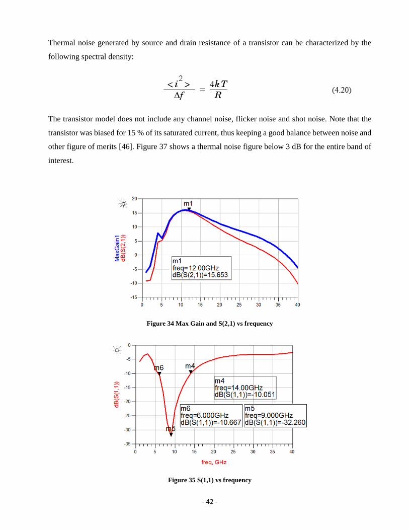
- 42 -
Thermal noise generated by source and drain resistance of a transistor can be characterized by the
following spectral density:
The transistor model does not include any channel noise, flicker noise and shot noise. Note that the
transistor was biased for 15 % of its saturated current, thus keeping a good balance between noise and
other figure of merits [46]. Figure 37 shows a thermal noise figure below 3 dB for the entire band of
interest.
Figure 34 Max Gain and S(2,1) vs frequency
Figure 35 S(1,1) vs frequency

- 43 -
Figure 36 S(2,2) vs frequency
Figure 37 Thermal Noise vs frequency
Table 4 shows a list of the largest contributors to noise in the LNA design. It can be seen that TFR1.R1
is the biggest contributor to the overall noise figure of the LNA design. TFR1.R1 is the feedback
resistor component from figure 25.
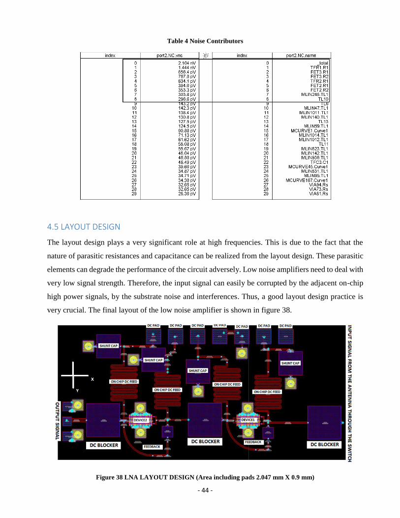
- 44 -
Table 4 Noise Contributors
4.5 LAYOUT DESIGN
The layout design plays a very significant role at high frequencies. This is due to the fact that the
nature of parasitic resistances and capacitance can be realized from the layout design. These parasitic
elements can degrade the performance of the circuit adversely. Low noise amplifiers need to deal with
very low signal strength. Therefore, the input signal can easily be corrupted by the adjacent on-chip
high power signals, by the substrate noise and interferences. Thus, a good layout design practice is
very crucial. The final layout of the low noise amplifier is shown in figure 38.
Figure 38 LNA LAYOUT DESIGN (Area including pads 2.047 mm X 0.9 mm)
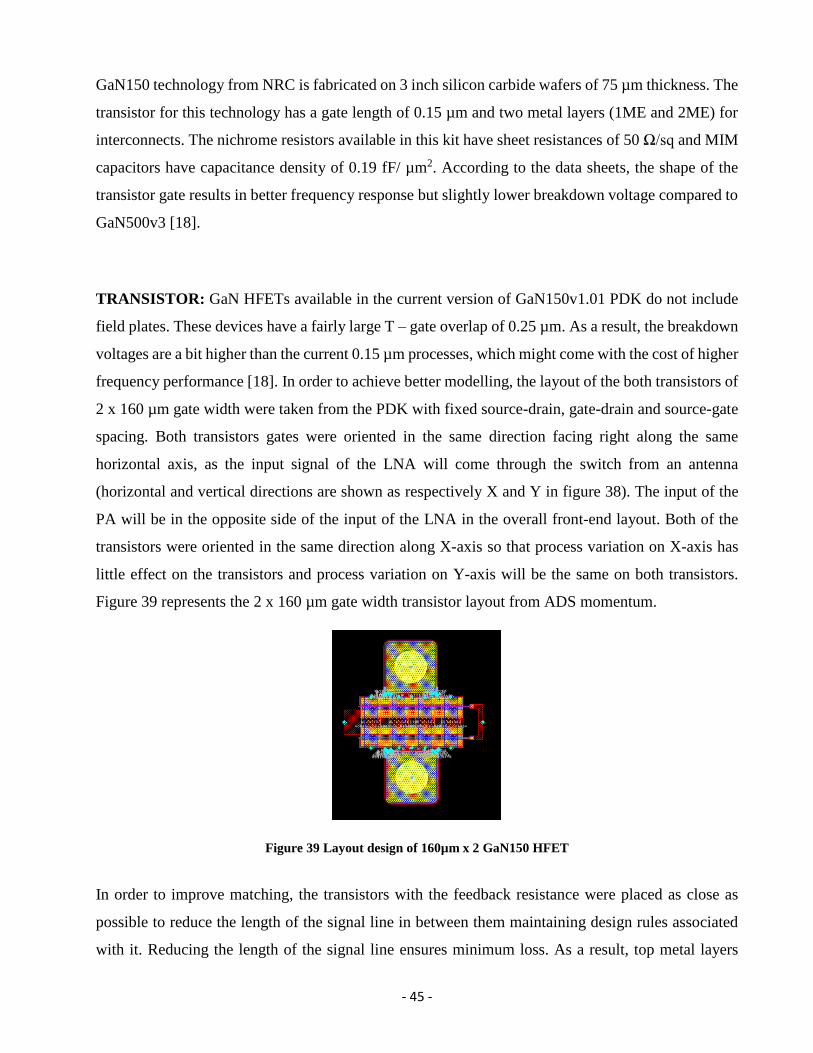
- 45 -
GaN150 technology from NRC is fabricated on 3 inch silicon carbide wafers of 75 µm thickness. The
transistor for this technology has a gate length of 0.15 µm and two metal layers (1ME and 2ME) for
interconnects. The nichrome resistors available in this kit have sheet resistances of 50 Ω/sq and MIM
capacitors have capacitance density of 0.19 fF/ µm2. According to the data sheets, the shape of the
transistor gate results in better frequency response but slightly lower breakdown voltage compared to
GaN500v3 [18].
TRANSISTOR: GaN HFETs available in the current version of GaN150v1.01 PDK do not include
field plates. These devices have a fairly large T – gate overlap of 0.25 µm. As a result, the breakdown
voltages are a bit higher than the current 0.15 µm processes, which might come with the cost of higher
frequency performance [18]. In order to achieve better modelling, the layout of the both transistors of
2 x 160 µm gate width were taken from the PDK with fixed source-drain, gate-drain and source-gate
spacing. Both transistors gates were oriented in the same direction facing right along the same
horizontal axis, as the input signal of the LNA will come through the switch from an antenna
(horizontal and vertical directions are shown as respectively X and Y in figure 38). The input of the
PA will be in the opposite side of the input of the LNA in the overall front-end layout. Both of the
transistors were oriented in the same direction along X-axis so that process variation on X-axis has
little effect on the transistors and process variation on Y-axis will be the same on both transistors.
Figure 39 represents the 2 x 160 µm gate width transistor layout from ADS momentum.
Figure 39 Layout design of 160µm x 2 GaN150 HFET
In order to improve matching, the transistors with the feedback resistance were placed as close as
possible to reduce the length of the signal line in between them maintaining design rules associated
with it. Reducing the length of the signal line ensures minimum loss. As a result, top metal layers

- 46 -
were used to implement interconnects and multiple metal-to-metal contacts were used in parallel to
reduce overall interconnect resistances.
As seen from figure 39, the sources of the transistor were connected with TWVs (Through-Wafer
vias). Multiple metal-to-metal connections were used to lower interconnect resistance. TWVs are
included to ensure a solid connection is made between the top surface and the backside ground using
holes through the substrate, which are connected with electroplated gold [18]. Therefore, it is possible
to realize low inductance ground connection as in microstrip design.
Figure 40 Through Wafer Via (TWV)
The NRC GaN foundry recommends that both sources separately need to be connected to ground,
therefore both sources were connected to TWVs. Besides air-bridges were used to connect both
sources of the transistors for better ground connection. They are formed in the metal 2 layer (2 ME)
using a nominally 2 µm thick removable resist layer to provide support [18].
FEEDBACK DESIGN:
The feedback path included the Metal1 layer connection between drain and gate, a 1 pF MIM
capacitor and a 230Ω nichrome resistor. The layout design of the gate and drain connection was
implemented using metal 1 layer and the length of the metal 1 layer (from the drain of the transistor
to the feedback resistor) was optimized to achieve 0.5nH of inductance, which was found to yield the
best results in section 4.4. The width of the Metal 1 layer was held constant at 10 µm. The layout
design for the feedback path and the inductance realized by the bend metal 1 connection are shown
in figures 41 and 42.
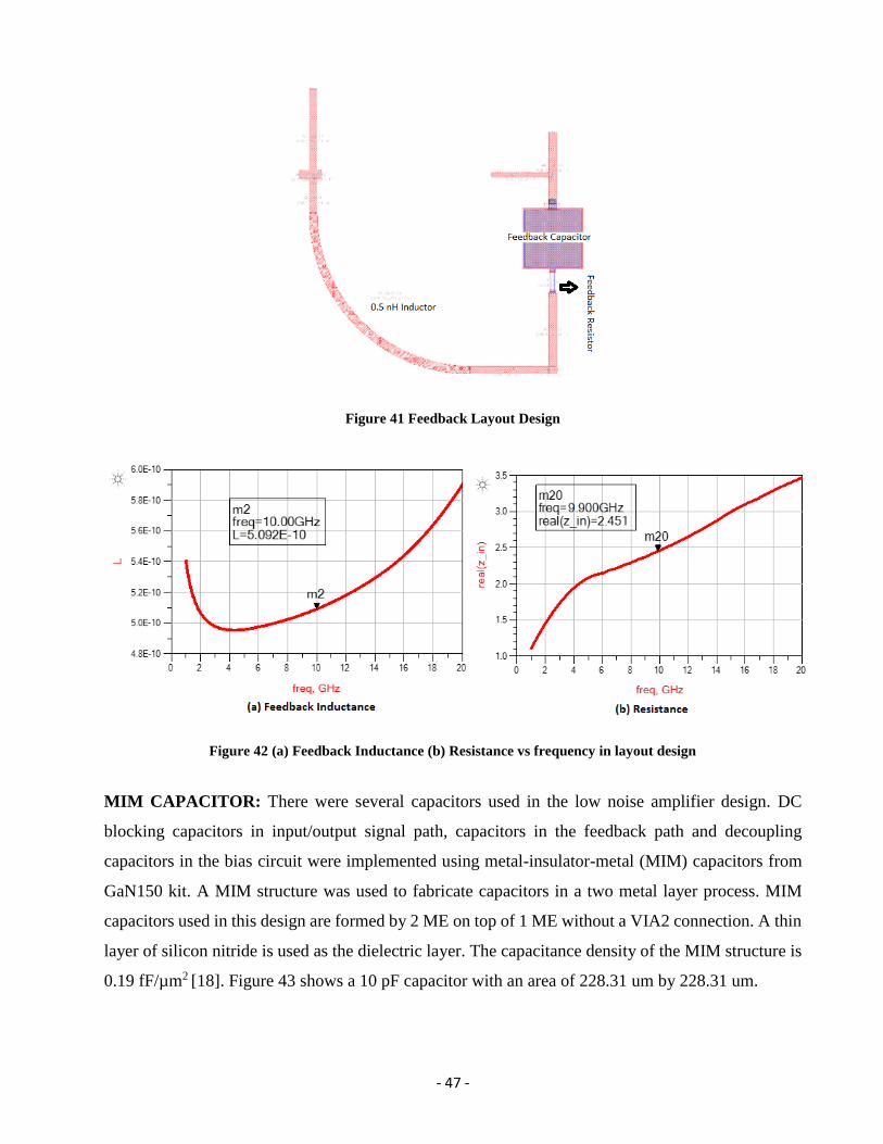
- 47 -
Figure 41 Feedback Layout Design
Figure 42 (a) Feedback Inductance (b) Resistance vs frequency in layout design
MIM CAPACITOR: There were several capacitors used in the low noise amplifier design. DC
blocking capacitors in input/output signal path, capacitors in the feedback path and decoupling
capacitors in the bias circuit were implemented using metal-insulator-metal (MIM) capacitors from
GaN150 kit. A MIM structure was used to fabricate capacitors in a two metal layer process. MIM
capacitors used in this design are formed by 2 ME on top of 1 ME without a VIA2 connection. A thin
layer of silicon nitride is used as the dielectric layer. The capacitance density of the MIM structure is
0.19 fF/µm2 [18]. Figure 43 shows a 10 pF capacitor with an area of 228.31 um by 228.31 um.

- 48 -
Figure 43 MIM Capacitor from GaN150 Design Kit
NICHROME RESISTOR: The shunt feedback resistors were implemented using nichrome (NiCr)
resistors from the design kit. These resistors are formed using a very thin layer of evaporated nichrome
with a contact of 1 ME layer. These resistors have a resistivity of 50 Ω/ sq. However, the current
carrying capability is significantly lower than that of the interconnect metals [18]. Figure 44 shows a
nicrome resistor from the design kit.
Figure 44 Nicrome Resistor from GaN150 Design Kit
BONDING PADS: The bonding pads offer a connection between the IC and the external circuitry.
There were of two types: one type is for RF connections and the other type is for DC connections
(Figures 45 and 46). The design used RF probes of 60 X 60 µm2 where signal to ground distance was
kept 100 µm and the distance from LNA signal to PA signal was kept 330 µm (because of probe
availability) in order to provide 50 Ω from the probing location all the way to the transmission line.
The design of DC pads is much simpler as there is no dependency on characteristic impedance. The
options for DC pad were limited due to the probe availability of the test lab. The only available DC

- 49 -
probe for testing required 9 pins with 100 X 100 µm2 area with 150 µm pitch. The ground probes
were connected to TWVs with multiple metal-to-metal connections to connect to ground.
Figure 45 DC pads used for LNA Design
Figure 46 Signal Pads Used in LNA Design
4.5.1 BIAS NETWORK DESIGN
The DC biasing network uses RF chokes and blocking capacitors. The RF chokes are designed to
have very high impedance over the design bandwidth. The bias network can be designed in several
ways.
Quarter wave transmission line with a radial stub: Due to parasitic effects, the shunt resonant
capacitor can face bandwidth limitations. The use of radial stubs can solve the issue and it can provide
an RF short connection at the resonant frequency. Besides acting as a short, this can provide better
bandwidth (Figure 47).
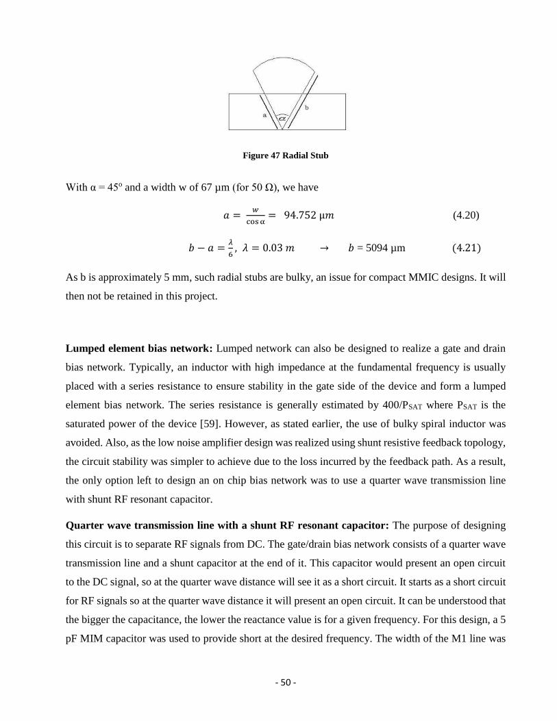
- 50 -
Figure 47 Radial Stub
With α = 45o and a width w of 67 µm (for 50 Ω), we have
𝑎 = 𝑤
cos α= 94.752 µ𝑚 (4.20)
𝑏 − 𝑎 =𝜆
6, 𝜆 = 0.03 𝑚 → 𝑏 = 5094 µm (4.21)
As b is approximately 5 mm, such radial stubs are bulky, an issue for compact MMIC designs. It will
then not be retained in this project.
Lumped element bias network: Lumped network can also be designed to realize a gate and drain
bias network. Typically, an inductor with high impedance at the fundamental frequency is usually
placed with a series resistance to ensure stability in the gate side of the device and form a lumped
element bias network. The series resistance is generally estimated by 400/PSAT where PSAT is the
saturated power of the device [59]. However, as stated earlier, the use of bulky spiral inductor was
avoided. Also, as the low noise amplifier design was realized using shunt resistive feedback topology,
the circuit stability was simpler to achieve due to the loss incurred by the feedback path. As a result,
the only option left to design an on chip bias network was to use a quarter wave transmission line
with shunt RF resonant capacitor.
Quarter wave transmission line with a shunt RF resonant capacitor: The purpose of designing
this circuit is to separate RF signals from DC. The gate/drain bias network consists of a quarter wave
transmission line and a shunt capacitor at the end of it. This capacitor would present an open circuit
to the DC signal, so at the quarter wave distance will see it as a short circuit. It starts as a short circuit
for RF signals so at the quarter wave distance it will present an open circuit. It can be understood that
the bigger the capacitance, the lower the reactance value is for a given frequency. For this design, a 5
pF MIM capacitor was used to provide short at the desired frequency. The width of the M1 line was
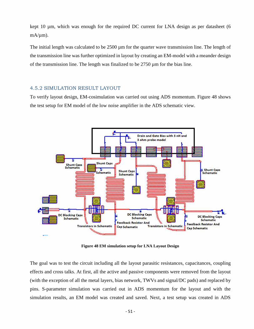
- 51 -
kept 10 µm, which was enough for the required DC current for LNA design as per datasheet (6
mA/µm).
The initial length was calculated to be 2500 µm for the quarter wave transmission line. The length of
the transmission line was further optimized in layout by creating an EM-model with a meander design
of the transmission line. The length was finalized to be 2750 µm for the bias line.
4.5.2 SIMULATION RESULT LAYOUT
To verify layout design, EM-cosimulation was carried out using ADS momentum. Figure 48 shows
the test setup for EM model of the low noise amplifier in the ADS schematic view.
Figure 48 EM simulation setup for LNA Layout Design
The goal was to test the circuit including all the layout parasitic resistances, capacitances, coupling
effects and cross talks. At first, all the active and passive components were removed from the layout
(with the exception of all the metal layers, bias network, TWVs and signal/DC pads) and replaced by
pins. S-parameter simulation was carried out in ADS momentum for the layout and with the
simulation results, an EM model was created and saved. Next, a test setup was created in ADS

- 52 -
schematic view with the EM model including the layout data and other active and passive
components.
S-PARAMETER SIMULATIONS: S-parameter simulations were carried out using the EM model
of the low noise amplifier connecting input and output port to 50 Ω. Required gate and drain bias
voltages (-3.76 V and 20 V, respectively) were provided to the transistors in both stages. Figures 49
and 50 show the S21 and max gain for the low noise amplifier layout. A gain degradation of 0.9 dB
(compared to figure 33) was observed with a max gain of 14.69 dB at 10 GHz.
Figure 49 Max Gain and S(2,1) vs frequency ( 5GHz to 40 GHz)
Figure 50 Max Gain and S(2,1) vs frequency (7 GHz to 16 GHz)

- 53 -
Figure 51 S(1,1) vs frequency
Figure 52 S(2,2) vs frequency
From figures 51 and 52, the feedback topology exhibits the desired response for input/output
matching. An input return loss better than 10 dB was achieved from 6 GHz to 14 GHz with a return
loss better than 34 dB at 9 GHz. An output return loss better than 10 dB was achieved from 3.8 GHz
to 15.5 GHz. The LNA layout design exhibited return loss better than 20 dB for the 7 to 11 GHz range
at the input and 5 to 12 GHz at the output. S-parameter simulation results are summarized in Table 5.

- 54 -
STABILITY: To check the circuit stability for the low noise amplifier, both the Rollett’s stability
factor K and stability measure B were plotted for frequency ranges from DC to 40 GHz. Figures 53
and 54 show that the stability factor is greater than 1 for the entire band of interest and the stability
measure was found to be greater than 0 as well. As discussed earlier although the feedback reduces
forward gain, it ensures unconditional circuit stability, which is very important for amplifier design.
Figure 53 Stability Factor (K) vs frequency
Figure 54 Stability Measure (B) vs frequency

- 55 -
NOISE: The noise figure results presented here take into account thermal noise associated with all
the resistances, including intrinsic model resistances, as well as losses from the overall layout. Figure
55 demonstrates that the noise figure is less than 3 dB in the entire band of interest.
Figure 55 Noise Figure (Thermal) vs frequency
1 dB COMPRESSION POINT: Harmonic balance simulations were carried out for one tone to find
out the 1 dB compression point of the low noise amplifier. RF power was varied from -40 to 15 dBm
at the input of the low noise amplifier. The maximum small signal gain was achieved for 10 GHz, as
a result 1 dB compression point was determined while keeping fundamental frequency at 10 GHz.
The bias conditions were kept the same as decided earlier. From figure 56, it can be seen that an
output referred 1 dB compression point of 13 dBm was achieved for 10 GHz.
TWO TONE HARMONIC BALANCE SIMULATIONS: Simulations with two fundamental tones
were performed to analyze the linearity performance of the low noise amplifier for 10 GHz
fundamental frequency with each frequency tone spaced by 0.01 GHz. Figures 57 and 58 show the
3rd order and 5th order IMD tones vs output power tones. The IMD tones are -20 dBc at 20 dBm output
power. The LNA will operate at much lower power than that, where the IMD tones are -120 dBc.

- 56 -
Figure 56 Gain vs Fundamental Output Power @10 GHz
Figure 57 High and Low Side Third Order IMD vs Fundamental Output Power Both Tones (dBc)
Figure 58 High and Low Side Fifth Order IMD (dBc) vs Fundamental Output Power Both Tones

- 57 -
Figure 59 shows an output referred IP3 (OIP3) of 25 dBm, which is approximately 12 dB higher than
the 1 dB compression point.
Figure 59 Third Order Intercept Point
4.6 DISCUSSIONS AND CONCLUSION
To the best of the author’s knowledge, the low noise amplifier designed in this thesis is the first X
band low noise amplifier designed and fabricated using NRC’s GaN 150 kit to achieve an overall
TX/RX front-end for 10 GHz. Comparing all the EM simulation results from table 5 in terms of gain,
input/output return loss and noise figure, excellent performance was achieved from 7 to 11 GHz with
more than 12 dB of gain and better than 20 dB return loss (input/output). An input return loss better
than 10 dB was achieved from 6 GHz to 14 GHz and an output return loss better than 10 dB was
achieved from 3.8 GHz to 15.5 GHz.
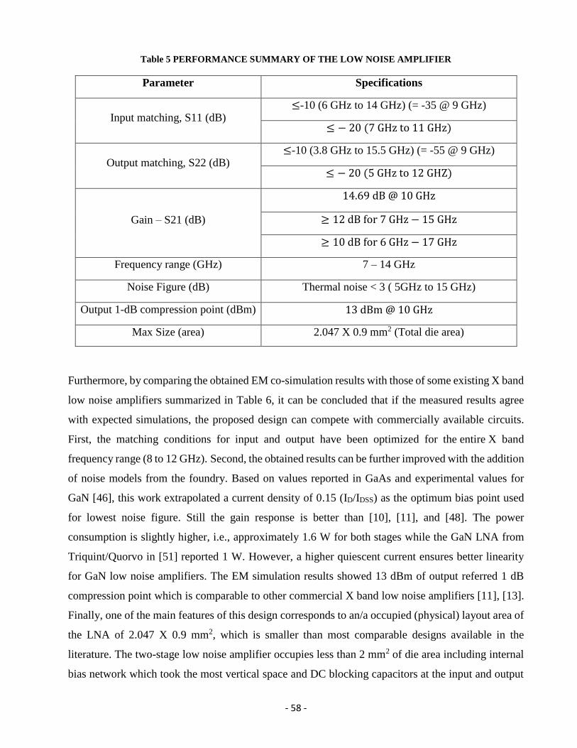
- 58 -
Table 5 PERFORMANCE SUMMARY OF THE LOW NOISE AMPLIFIER
Parameter Specifications
Input matching, S11 (dB) ≤-10 (6 GHz to 14 GHz) (= -35 @ 9 GHz)
≤ − 20 (7 GHz to 11 GHz)
Output matching, S22 (dB) ≤-10 (3.8 GHz to 15.5 GHz) (= -55 @ 9 GHz)
≤ − 20 (5 GHz to 12 GHZ)
Gain – S21 (dB)
14.69 dB @ 10 GHz
≥ 12 dB for 7 GHz − 15 GHz
≥ 10 dB for 6 GHz − 17 GHz
Frequency range (GHz) 7 – 14 GHz
Noise Figure (dB) Thermal noise < 3 ( 5GHz to 15 GHz)
Output 1-dB compression point (dBm) 13 dBm @ 10 GHz
Max Size (area) 2.047 X 0.9 mm2 (Total die area)
Furthermore, by comparing the obtained EM co-simulation results with those of some existing X band
low noise amplifiers summarized in Table 6, it can be concluded that if the measured results agree
with expected simulations, the proposed design can compete with commercially available circuits.
First, the matching conditions for input and output have been optimized for the entire X band
frequency range (8 to 12 GHz). Second, the obtained results can be further improved with the addition
of noise models from the foundry. Based on values reported in GaAs and experimental values for
GaN [46], this work extrapolated a current density of 0.15 (ID/IDSS) as the optimum bias point used
for lowest noise figure. Still the gain response is better than [10], [11], and [48]. The power
consumption is slightly higher, i.e., approximately 1.6 W for both stages while the GaN LNA from
Triquint/Quorvo in [51] reported 1 W. However, a higher quiescent current ensures better linearity
for GaN low noise amplifiers. The EM simulation results showed 13 dBm of output referred 1 dB
compression point which is comparable to other commercial X band low noise amplifiers [11], [13].
Finally, one of the main features of this design corresponds to an/a occupied (physical) layout area of
the LNA of 2.047 X 0.9 mm2, which is smaller than most comparable designs available in the
literature. The two-stage low noise amplifier occupies less than 2 mm2 of die area including internal
bias network which took the most vertical space and DC blocking capacitors at the input and output

- 59 -
stage. In summary, the designed low noise amplifier exhibits excellent performance vs. exiting
designs while meeting the design specifications.
Table 6 LNA PERFORMANCE COMPARISON WITH OTHER X BAND LNA
*: Commercial chip **: thermal noise
Ref
Frequency
Range
(GHz)
S21
(dB) NF (dB)
Power
dissipation S11 (dB)
S22
(dB)
P1dB
dBm
OIP3 Technology Size
mm2
[10] 9-13 ≥ 10 ≤ 2.9 ≤ −6.5 -- -- Al0.25Ga0.75N 2.2 x 1.3
[11] --
18.5
@ 10
GHz
2.3 @ 10
GHz
-10 @
10 GHz
-10
@ 10
GHz
-- --
0.25 µm
AlGaN/GaN
HEMT
2.6 x 1.1
[46] 8-11 20 2.5 1 ≤-10 ≤-10 17 -- GaN – HEMT
technology 3.0 x 2.1
[47] 7-12 14 2.5 -- -10 -- 20 28
0.25 µm
AlGaN/GaN
HEMT
2.5 x 2
[48] 4-16 11 2 -- -10 -- -- 24
AlGaN/GaN
HEMT
microstrip
[49] 8-11 17 1.8 -- -10 -- 22 26
AlGaN/GaN
HEMT
microstrip
[50] 8-11 20 2.5 -- -5 -- 20 --
QinetiQ
AlGaN/GaN
CPW
2.3 x 4.3
[51] *
2-22 15 2 1 W -- -- 22
0.25 GaN
HEMT
2.04 x
1.49
[52] *
6-14 20 1.3 800 mW -18 -18
12
0.15 3MI
PHEMT
2.05 X
1.20
[53] *
5-15 27 1.4 800 mW -15 -20 13 25
0.15 3MI
PHEMT
2.05 x
1.20
This work 7-14 ≥ 𝟏𝟐 < 3 ** 1.6 watt -20 -20 13 25 0.15 µ GaN
HFET
2.047 x
0.9

- 60 -
CHAPTER 5 POWER AMPLIFIER BACKGROUND
5.1 DEFINITION AND KEY DESIGN PARAMETER
Power amplifiers (PAs) are one of the most significant design blocks in the transmitter side of a
transceiver system. Compared to LNAs, PAs do not have to deal with unknown signals. Also, a LNA
is a linear amplifier while a PA is a nonlinear amplifier. Therefore, their design approaches are quite
different. For linear and quasi-linear amplifiers, the design is achieved from the small-signal S
parameters of the transistor. However, the small-signal approaches can be still used for large-signal
amplifiers operating in class A (i.e., with an almost linear output power) but they are not suitable for
the other classes such as AB, B, C, D, E, F, G, H, or S. For power (nonlinear) amplifiers, the design
is achieved through load-pull transistor characterization: the load is determined to allow maximum
output power or efficiency. The source is then conjugate matched to ensure maximum power transfer
[60], [61].
Linearity and efficiency are the two most important design parameters for power amplifiers. PAs
require the most amount of DC power in the transmitter chain. Efficiency is the measure of how much
of this DC power is actually converted to RF [20].
The significance of linearity in RF systems and low noise amplifiers was discussed in previous
chapters. If the PA is nonlinear, the energy associated in unwanted harmonics and intermodulation
signals can cause DC power loss. Therefore, linearity and efficiency are correlated [20].
5.2 CLASSES OF OPERATION
Power amplifiers are categorized by classes. The DC operating point of the power amplifier
determines its class. The conduction angle of the current passing through the transistor in a certain
bias point varies in different classes of power amplifiers. If desired class of operation is class A, then
conduction angle of 360o is required. That will keep the device always ON which results in good
linearity but degrades the efficiency of the amplifier. In other words, it can be said that operating
points are also based on efficiency. Linearity of the amplifier gets worse with the chronological order
of alphabetic classes [20]. Therefore, class AB is one of the most favorable, as this class is a
compromise between linearity and efficiency [20]. Figure 60 shows the load lines for each of the
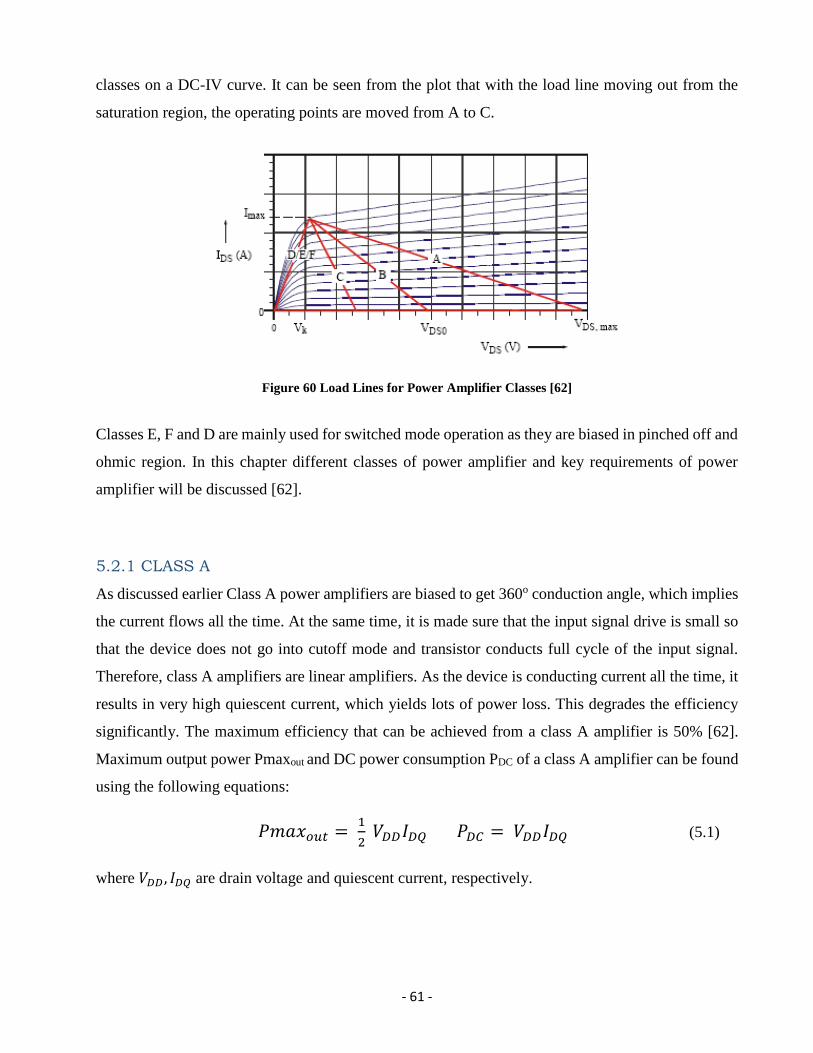
- 61 -
classes on a DC-IV curve. It can be seen from the plot that with the load line moving out from the
saturation region, the operating points are moved from A to C.
Figure 60 Load Lines for Power Amplifier Classes [62]
Classes E, F and D are mainly used for switched mode operation as they are biased in pinched off and
ohmic region. In this chapter different classes of power amplifier and key requirements of power
amplifier will be discussed [62].
5.2.1 CLASS A
As discussed earlier Class A power amplifiers are biased to get 360o conduction angle, which implies
the current flows all the time. At the same time, it is made sure that the input signal drive is small so
that the device does not go into cutoff mode and transistor conducts full cycle of the input signal.
Therefore, class A amplifiers are linear amplifiers. As the device is conducting current all the time, it
results in very high quiescent current, which yields lots of power loss. This degrades the efficiency
significantly. The maximum efficiency that can be achieved from a class A amplifier is 50% [62].
Maximum output power Pmaxout and DC power consumption PDC of a class A amplifier can be found
using the following equations:
𝑃𝑚𝑎𝑥𝑜𝑢𝑡 = 1
2 𝑉𝐷𝐷𝐼𝐷𝑄 𝑃𝐷𝐶 = 𝑉𝐷𝐷𝐼𝐷𝑄 (5.1)
where 𝑉𝐷𝐷 , 𝐼𝐷𝑄 are drain voltage and quiescent current, respectively.

- 62 -
5.2.2 CLASS B
Class B amplifiers are biased to achieve 180o of conduction angle, which implies a conduction either
in the positive or negative half cycle of the input signal. This class can be achieved by biasing the
transistor at its cut off or zero quiescent current region so that any current passing through the device
directly goes to the load. The theoretical maximum efficiency of a class B amplifier is 78.5% at peak
envelope power as the device conducts only for half of the cycle [62]. But this creates more distortion
in RF output signal. Therefore, the efficiency will come with the cost of linearity. The DC power
consumption of class B amplifier is stated by the following equation:
𝑃𝐷𝐶 = 2
𝜋 𝑉𝐷𝐷𝐼𝐴𝐶_𝑚𝑎𝑥 (5.2)
Where 𝑉𝐷𝐷 , 𝐼𝐴𝐶_𝑚𝑎𝑥 state for drain voltage and maximum AC output current, respectively.
Class B amplifiers are generally designed using push pull structure where two transistors are used in
parallel [63]. In this structure, one transistor conducts in the positive half cycle and the other one in
negative half cycle. In this way, the entire input signal is used and replicated in the output signal.
5.2.3 CLASS C
Class C amplifiers are theoretically the most efficient among these classes of amplifier. The efficiency
can go up to 85 %. Class C amplifiers are biased so that the conduction angle is significantly lower
than 180o. It is achieved in a way that the output current is almost zero for more than half the cycle of
the input signal [62]. But as discussed earlier, there is a solid correlation between conduction angle to
linearity and efficiency. As being the most efficient class, the linearity of this class is the worst among
these four classes. Due to high nonlinearity, class C amplifiers are not used for high frequencies.
5.2.4 CLASS AB
Class AB is the true balance between linearity and efficiency, as the bias configuration is just in-
between class A and class B. The transistor is biased between cutoff and class A bias point which
implies conduction angle less than 360o but greater than 180o [62]. The device is turned on for more
than half of the cycle. The linearity of class AB amplifier can be similar to class A and theoretical
efficiency can range from 50 % to 78.5 % [62].

- 63 -
5.2.5 ADDITIONAL POWER CLASSES
Power amplifier operating in class D, E, F, G, H, or S, are geared significantly towards higher
efficiency performance. These classes are widely used for narrowband tuned amplifiers where
linearity is not a big concern but efficiency is [62].
Different techniques are used to increase efficiency. For example, switching technique is used in class
D, E, and S. Harmonic resonators are used in the output stage of class F amplifiers to shape the drain
waveforms [64]. Resonators and multiple power supply voltages are used in class G and H [64].
5.3 POWER AMPLIFIER PERFORMANCE METRICS
PA will deliver the maximum required power of the transmitter keeping the spurious emissions as
low as possible with its linearity. Since the PA consumes the most amount of power in the transceiver,
it is very important to find out how efficiently supplied DC power is converted to RF power while
transmitting the required power level. That is why the two most important performance metrics for
PA are linearity and efficiency. In addition to linearity and efficiency, the other performance metrics
are noise figure and stability.
Generally, efficiency is a way to determine device’s capacity to convert one source of energy to
another. In power amplifier theory, the efficiency indicates the amplifier’s ability to convert DC
power of the supply into the RF power delivered to the load. The thermal dissipation is the result of
the energy, which is not converted to the desired RF signal. That is why thermal dissipation of an
amplifier is correlated with efficiency. The maximum efficiency of a power amplifier depends on
classes of operation (as discussed above), input drive level, frequency, load impedance, temperature
and bias point. It can also depend on device geometry and intrinsic device characteristics. In RF design
the efficiency can be measured in three ways, drain efficiency, power added efficiency, and total
efficiency [65].
Drain efficiency is the direct ratio of output power to input DC power. It can be shown as [65]:
Ƞ =𝑃𝑅𝐹𝑜𝑢𝑡
𝑃𝐷𝐶=
𝑃𝑅𝐹𝑜𝑢𝑡
𝑉𝐷𝐶 . 𝐼𝐷𝐶 (5.3)
The disadvantage of using this figure of merit is that the input RF power is not taken into
consideration.

- 64 -
Power added efficiency (PAE) takes into account the input RF power while calculating efficiency.
This is the most recognized figure of merit when comparing single amplifiers. When the PAE and
drain efficiency are not the same the device does not have linear gain anymore. The equation for PAE
is given below (5.7) [65]. From the equation, it can be seen that PAE will always be less than the
drain efficiency unless the gain is very high [65].
𝑃𝐴𝐸 = 𝑃𝑅𝐹𝑜𝑢𝑡− 𝑃𝑅𝐹𝐼𝑁
𝑃𝐷𝐶=
𝑃𝑅𝐹𝑜𝑢𝑡− 𝑃𝑅𝐹𝐼𝑁
𝑉𝐷𝐶 𝐼𝐷𝐶 (5.4)
Total efficiency is the complete picture of the ratio of output power to all input power (DC and RF).
Equation (5.8) shows the total efficiency [65]. But PAE is still the most favored measure for efficiency
in power amplifiers as this is specific to a particular input power value. [8]
Ƞ𝑡𝑜𝑡𝑎𝑙 =𝑃𝑅𝐹𝑜𝑢𝑡
𝑃𝐷𝐶+𝑃𝑅𝐹𝐼𝑁=
𝑃𝑅𝐹𝑜𝑢𝑡
𝑉𝐷𝐶 . 𝐼𝐷𝐶 + 𝑃𝑅𝐹𝐼𝑁 (5.5)
5.4 CONCLUSION
As explained in this chapter, there is generally a compromise between linearity and efficiency while
designing the PA. Power amplifiers can operate at back off power level from the peak output power
in the linear and efficient region to emphasize on linearity requirement, which is basically class AB
operation. Alternatively, the PA can be designed in class B bias condition to get the maximum
efficiency but that is a very nonlinear situation. One of the goal of this thesis is to design a power
amplifier operating at X band to achieve an overall front-end design for 10 GHz. Since the frequency
of operation was 10 GHz and GaN power density is very high with a big swing in the drain voltage,
the PA was designed in class AB to have a balance between linearity and PAE.

- 65 -
CHAPTER 6 X BAND POWER AMPLIFIER DESIGN
6.1 REQUIREMENTS OF X BAND POWER AMPLIFIER
In this section, a two-stage common source class AB MMIC power amplifier will be designed and
simulated to achieve an overall 10 GHz RF front-end module for future wireless systems. There are
several compact power amplifier chips available by Triquint/Qorvo and Analog devices with similar
specifications, which will be shown in the review section of this chapter. To be noted, this is the first
time GaN150 has been available to Canadian researchers. The GaN 150 kit version 1.01 used to
implement this PA design features a measured power density of 7watt/mm at 8 GHz [18]. As a result,
a PA will be designed to deliver 2 W (33 dBm) to a 50 Ω antenna port at 10 GHz to target X band.
The output of the PA will be connected to a transmit/receive (T/R) switch in the front-end architecture.
The switch (to be designed by another researcher) will be matched to 50 Ω for both PA and LNA
sides. In order to maintain such symmetry, the design methodology of the power amplifier will
concentrate on realizing optimum power and efficiency for a 50 Ω port Antenna. A compromise
should be then made to the PA efficiency and output power due to the 50 Ω load impedance. To
further evaluate the impact of this tradeoff, simulations will be conducted using the optimum load
value and then it will be compared to a 50 Ω load response. Also, two of the most important features
of the designed power amplifier are its size to validate its power density and simplicity of its physical
design to increase its immunity to process variations. Table 7 shows the design specifications for the
PA.
Table 7 X band PA Design Specifications
PARAMETER DESIGN SPECIFICATIONS
Operating Frequency 10 GHz
Bandwidth 8 – 12 GHz
Output Power 2 W (33 dBm)
Gain @ output power > 15 dB
Power Added Efficiency @ 2 watt > 25 %
Die area < 2 mm2

- 66 -
6.2 LITERATURE REVIEW
As stated in the technical literature, the high breakdown voltages, high power densities and strong
performance at higher frequencies make GaN technology an ideal candidate for RF power
applications. In [59], a 0.5-6.5 GHz distributed PA was designed using the GaN500 process provided
by NRC. A peak PAE of 38.1 % was obtained by the amplifier at 0.5 GHz while a nominal PAE of
20 % was achieved over the entire band (0.5 GHz – 6.5 GHz) with an output power of 1 W. In [66],
a 10 GHz power amplifier was designed in class AB with harmonic filters using a GaN 0.8 µm HFET
9-layer process with a DC bias line and input/output matching being built on a low cost miniature-
hybrid MIC chip. Simulation results showed 39 dBm output power maintaining 31 % PAE. However,
the fabricated PA suffered from overheating due to the used flip chip technique and measured results
yielded a PAE of 4% at 8GHz while outputting 28.5 dBm power. In [67], a 2-18 GHz distributed
power amplifier was designed using GaN 0.2µm process. The low inter-stage impedance of 25 Ω,
used to achieve larger size HEMTs in the output stage, increased the output power without reducing
the bandwidth. This also ensured inter-stage transmission lines to be shorter. Measured 20 dB small
signal gain for the entire band and peak saturated power of 2 W was reported. In [68], two MMIC
power amplifiers were designed using 0.25µm GaN HEMT process, one for S band and the other one
for X band, reporting a maximum output power of 4.8 W for X band.
The commercial design close to our specifications is the HMC487, a 9-12 GHz GaAs HEMT power
amplifier by Hittite Microwave Corp [14]. Internally matched, it can generate 1W RF output with a
10 mW input power. In its data sheet 20 dB of gain for the entire band and a peak PAE of 20 % at 10
GHz with 2 W output power was reported. Several X band power amplifier chips have been reported
by Triquint using their GaN power PHEMT process with similar power specifications [69]-[72].
The only work with similar power specifications using the GaN 0.15µ process was reported in [73].
This is a PA driver amplifier for Ku band from Triquint/ Qorvo. The performance merits of these X
band commercial/research works will be compared to the proposed PA results.
6.3 DESIGN PROCEDURE
The first step was to determine the size of the required GaN HFET (i.e. number of fingers and
unity gate width) suitable for the required power levels identified in Table 7.
DC analysis was conducted on the selected transistor to determine the required bias voltages
for Class AB operation.

- 67 -
Verification of both the transit frequency (fT) and maximum frequency (fmax) at the required
bias levels was performed to ensure optimum PA performance at 10 GHz.
A circuit schematic was built with design kits and custom EM models.
ON chip DC bias network was designed to supply required bias voltages.
Large signal harmonic balance simulations were conducted to obtain the gate bias voltage in
class AB operation range that ensures the optimum efficiency and maximum output power
delivered to a 50 Ω load.
Load Pull harmonic balance simulations were conducted to obtain the optimum load.
Next, the output power delivered to an optimum load and associated power added efficiency
was compared to a 50 Ω load response.
Layout design of the class AB power amplifier was constructed to be integrated with the low
noise amplifier and the switch design to conceive a 10 GHz front-end design.
Large signal harmonic balance simulations and S-parameter simulations were conducted using
EM model of the PA layout design to verify design requirements.
6.4 DEVICE SIZING
Two design parameters are available for the GaN150 HFETs in the design kit: unity gate width W
and spacing between two gates. The model offers two gate devices in version 1.1. The NRC design
kit manual recommends that single gate width is to be kept below 250 µm. To increase the power gain
of the PA, it was decided to use two gain stages in series. With reference to NRC foundry design
manual [18] the design required the first and second stages each to have a total gate width of 200 µm
(100 µm (each finger width) x 2 (no of finger)) to achieve the required output power of 2 W. In order
to improve immunity to process variations, the device size used default gate distances of 48.7 µm.
6.5 DC ANALYSIS
DC analysis is a very important design step for a power amplifier design. Currently reported narrow-
band GaAs/GaN devices are generally using 15-20 V DC supply. As a result, it was decided to provide
20 V DC supply to the PA. Following the design foundry manual [18], the gate voltage was varied
from -8 V to 2 V and the associated drain current plotted in Figure 61. From this figure, it is
demonstrated that the current keeps increasing in the saturation region. The HFET model is built
based on channel length modulation [59]. This is indicative that the current is not constant in the
saturation region as in the ideal model, rather it increases with a slope of 1/r0 [59]. Figure 61 also

- 68 -
demonstrates at -4.4 V of gate voltage, the associated current is 1 mA. By conducting small and large
signal simulations, it was verified that no gain could be obtained before applying -4.3 V to the gate.
Hence, from the amplification perspective, deep class AB range was decided up to -4 volts. However,
the bias point close to shut down voltage will not be able to provide sufficient power and
consequently, the linearity performance will also deteriorate, which are the major design requirements
for this amplifier design beside power added efficiency.
Figure 61 Drain Current vs Gate Voltage with 20 V Drain Supply Voltage
While conducting DC simulation, the drain voltage was varied from 0.1 V to 40 V while the gate
voltage was varied from -4 V to 0 V, in order to avoid the high current shoot due to the transistor
model after saturation. The current level after saturation for gate to source voltage of 0.5, 1 and 2 volts
were approximated from the measured current density level provided in the NRC design manual [18].
From figure 62, class A operation was selected for gate voltage equals to -1 V. From figure 62, class
AB operation can be achieved for a range of gate voltage from -3.9 V to -1.1 V. Therefore, in order
to obtain expected power and linearity performance, the gate was initially biased at -2.5 V knowing
that this value has to be adjusted depending on the large signal simulations for maximum power and
power added efficiency to be conducted in section 6.6.1.
Figure 63 shows the saturated drain current and the drain current levels for a gate voltage of -2.5 V.
The DC current is approximately 91 mA. A verification of the operating conditions for transit
frequency and maximum frequency followed and the results are shown in figures 64 and 65. Results

- 69 -
from these figures show that the unity gain frequency is 38 GHz and maximum frequency is 47 GHz
for the selected class AB bias point.
Figure 62 Drain Current vs Gate Voltage for different Gate Voltage
Figure 63 Drain Current vs Gate Voltage with 20 V DC supply
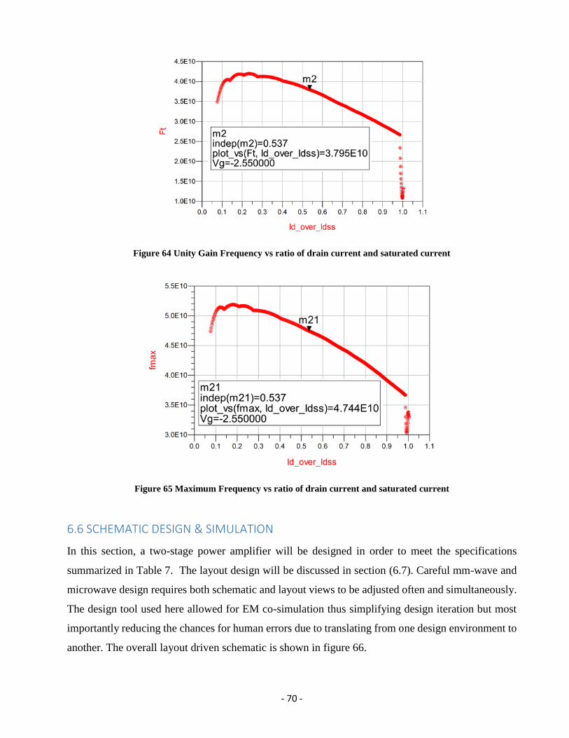
- 70 -
Figure 64 Unity Gain Frequency vs ratio of drain current and saturated current
Figure 65 Maximum Frequency vs ratio of drain current and saturated current
6.6 SCHEMATIC DESIGN & SIMULATION
In this section, a two-stage power amplifier will be designed in order to meet the specifications
summarized in Table 7. The layout design will be discussed in section (6.7). Careful mm-wave and
microwave design requires both schematic and layout views to be adjusted often and simultaneously.
The design tool used here allowed for EM co-simulation thus simplifying design iteration but most
importantly reducing the chances for human errors due to translating from one design environment to
another. The overall layout driven schematic is shown in figure 66.
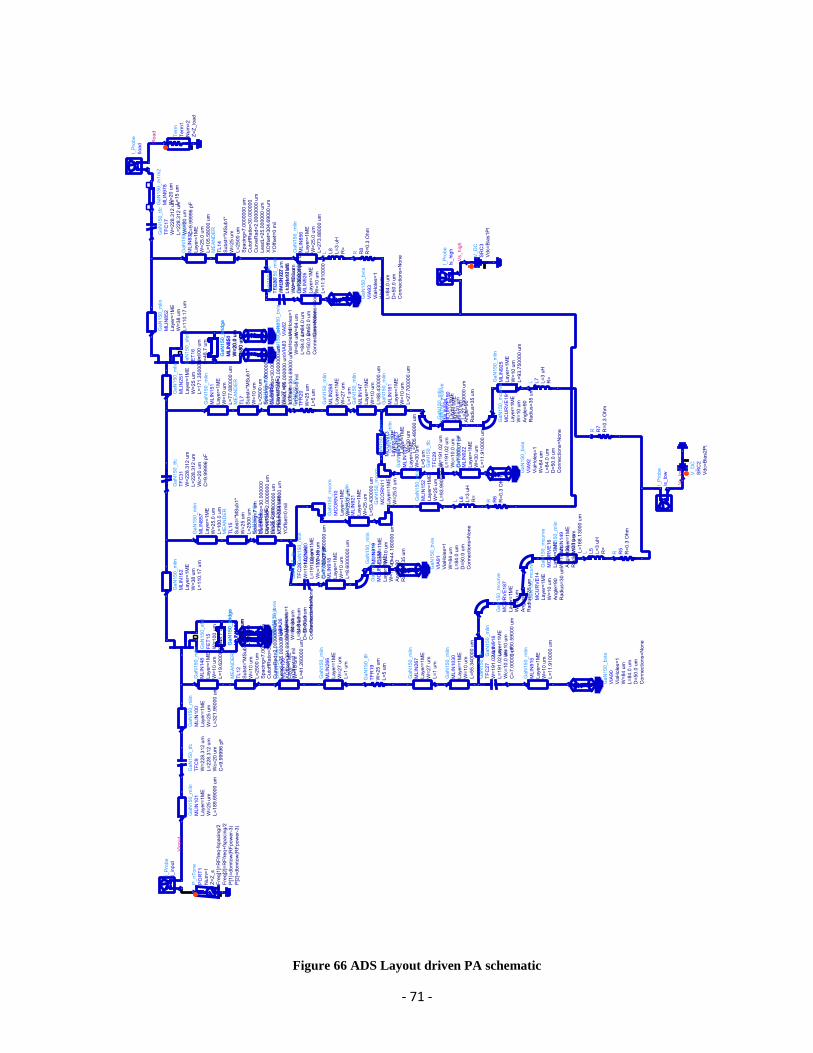
- 71 -
Figure 66 ADS Layout driven PA schematic

- 72 -
6.6.1 BIAS VOLTAGE OPTIMIZATION
As mentioned earlier, the output of the power amplifier will be fed through a transmit/receive switch
matched to 50 Ω. Large signal harmonic balance simulations were conducted connecting 50 Ω port
at the input/output port of the power amplifier. RF signal levels of 18 dBm were provided at the input
of the power amplifier to achieve approximately 2 W of output power. A 20 Volt drain supply voltage
was used while the gate bias was varied between -1.5 V and -3.7 V for class AB operation. Figure 67
shows an increase in the power added efficiency, PAE, when the bias point of the PA was moved
closer to the transistor cut-off region. In contrast, Figure 68 shows the PA output power decreased,
illustrating design trade-offs between output power and efficiency. Therefore, -2.3 V was selected to
be used as optimum gate bias voltage. From figures 67 and 68, an output power of 34 dBm can be
obtained with 30 % of power added efficiency using gate voltage of -2.3 V.
However, to verify the output power and PAE further with this bias condition (-2.3 V), input power
was varied at the input of the power amplifier schematic conducting harmonic balance simulations
(figures 69 and 70). In the next section, load pull using large signal harmonic balance simulations will
be performed using the selected bias voltage to find out the optimum load for the power amplifier to
understand the degradation of the PA output power and efficiency compared to a 50 Ω load.
Figure 67 PAE vs Gate Bias Voltage
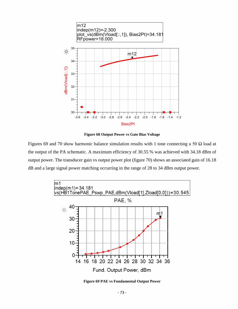
- 73 -
Figure 68 Output Power vs Gate Bias Voltage
Figures 69 and 70 show harmonic balance simulation results with 1 tone connecting a 50 Ω load at
the output of the PA schematic. A maximum efficiency of 30.55 % was achieved with 34.18 dBm of
output power. The transducer gain vs output power plot (figure 70) shows an associated gain of 16.18
dB and a large signal power matching occurring in the range of 28 to 34 dBm output power.
Figure 69 PAE vs Fundamental Output Power

- 74 -
Figure 70 Power Gain vs Fundamental Output Power
6.6.2 OPTIMUM LOAD SELECTION
Load pull simulation is used to determine the optimum complex output impedance the PA requires in
order to either deliver a) maximum power or b) maximum power added efficiency. Load pull
simulation was conducted using 1 tone harmonic balance simulation varying complex load at the
output of the PA schematic to obtain the optimum load for the PA design. RF signal levels of 18 dBm
were provided at the input of the power amplifier. Figure 71 shows PAE and power contours from the
load pull simulation results. From figure 71 it can be seen that the load impedance for maximum PAE
and power was found to be very close. An optimum load value of 21.5 + j4.356 Ω was found to yield
the maximum power of 35.5 dBm having the input of the PA matched to 50 Ω. A circuit realization
of this load is capable of providing 35.5 dBm of output power with a power added efficiency close to
33.5 % from the power amplifier design.
The use of bulky spiral inductor from GaN150 kit was avoided for this thesis work because of its
performance issue. As a result, the circuit realization of the matching network to realize the required
optimum load can use a quarter wave length transmission line. With the substrate parameters defined
in the GaN 150 Foundry Design Manual [18] the length and width of the quarter wave length
transmission line was found to be approximately 2700 µm and 67 µm respectively, which is definitely
too large for the specified layout area from table 7.
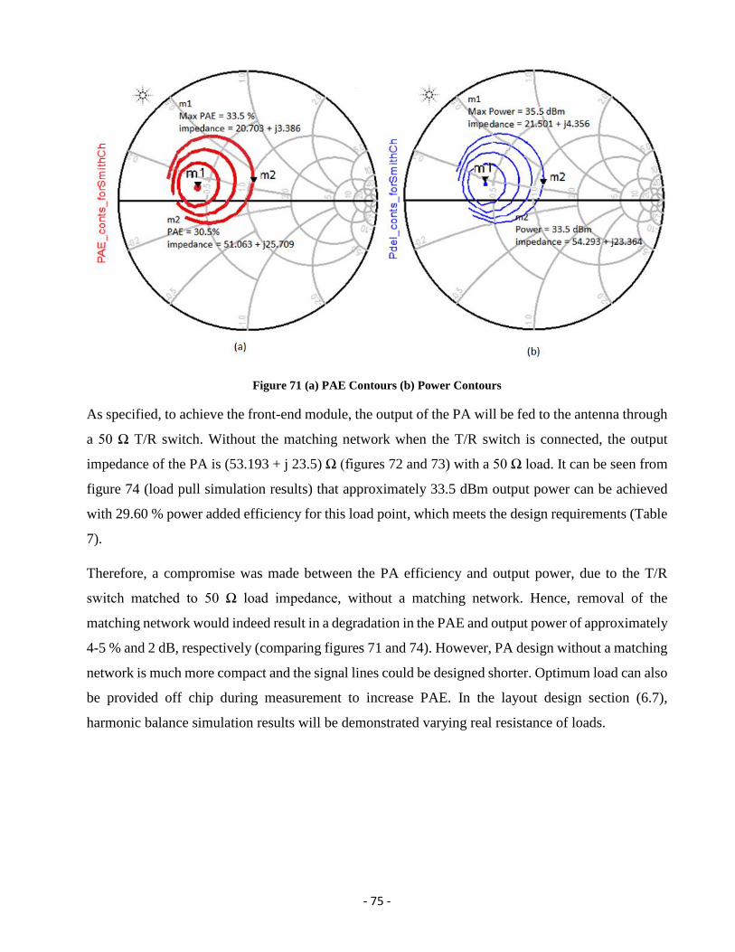
- 75 -
Figure 71 (a) PAE Contours (b) Power Contours
As specified, to achieve the front-end module, the output of the PA will be fed to the antenna through
a 50 Ω T/R switch. Without the matching network when the T/R switch is connected, the output
impedance of the PA is (53.193 + j 23.5) Ω (figures 72 and 73) with a 50 Ω load. It can be seen from
figure 74 (load pull simulation results) that approximately 33.5 dBm output power can be achieved
with 29.60 % power added efficiency for this load point, which meets the design requirements (Table
7).
Therefore, a compromise was made between the PA efficiency and output power, due to the T/R
switch matched to 50 Ω load impedance, without a matching network. Hence, removal of the
matching network would indeed result in a degradation in the PAE and output power of approximately
4-5 % and 2 dB, respectively (comparing figures 71 and 74). However, PA design without a matching
network is much more compact and the signal lines could be designed shorter. Optimum load can also
be provided off chip during measurement to increase PAE. In the layout design section (6.7),
harmonic balance simulation results will be demonstrated varying real resistance of loads.

- 76 -
Figure 72 Output Impedance (Real) of the PA connecting SPDT at the output
Figure 73 Output Impedance (Imaginary) of the PA connecting SPDT at the output
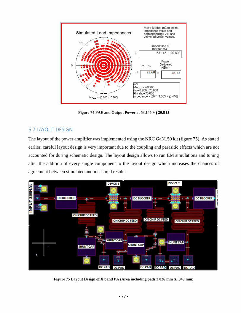
- 77 -
Figure 74 PAE and Output Power at 53.145 + j 20.8 Ω
6.7 LAYOUT DESIGN
The layout of the power amplifier was implemented using the NRC GaN150 kit (figure 75). As stated
earlier, careful layout design is very important due to the coupling and parasitic effects which are not
accounted for during schematic design. The layout design allows to run EM simulations and tuning
after the addition of every single component to the layout design which increases the chances of
agreement between simulated and measured results.
Figure 75 Layout Design of X band PA (Area including pads 2.026 mm X .849 mm)

- 78 -
The layout uses GaN HFETS models available in the current version of GaN150v1.01 PDK. In order
to achieve better modelling, the layout of the both transistors of 2 x 100 µm gate width were taken
from the PDK with fixed source-drain, gate-drain and source-gate spacing. Both transistors gates were
oriented in the same horizontal direction facing left X axis opposite to the low noise amplifier input
signal as the output of the power amplifier will go through the switch to an antenna. Figure 75 shows
the references for horizontal X-axis and vertical Y-axis. As a result, process variation on X-axis has
little effect on the transistors and process variation on Y-axis will be the same on both transistors. To
achieve better device matching, both transistors were placed as close as possible lowering the signal
line length in between while meeting all design rules. From figures 38 and 75, with comparison to the
low noise amplifier layout design, the power amplifier layout design used wider interconnect metals
in order to ensure higher power requirement of the power amplifier comply with transmission line
maximum current ratings for the required line widths.
The required DC blocking capacitors at the input/output signal path and decoupling capacitors in the
bias circuit were implemented using MIM capacitors from the design kit. Two small nichrome (NiCr)
resistors with a value of 10 Ω (width = 25 µm and length = 5 µm) were used in the gate bias lines of
the power amplifier to ensure unconditional stability of the power amplifier.
The bonding pads used in the input/output connections and DC connections in power amplifier layout
are identical to the low noise amplifier due to the availability of the probes for measurement. The
design used RF probes with dimensions of 60 X 60 µm2. The distance between signal probe and
ground probe was 100 µm and the distance between two signal probes was 330 µm. The PA design
used 6 DC pads each with dimensions of 100 X 100 µm2. The distance between 2 adjacent DC pads
was 150 µm.
6.7.1 BIAS NETWORK DESIGN
A transmission line feed with a quarter wave length and a shunt capacitor was designed for the gate
and drain bias voltage supply of both PA stages. The width of the drain bias network was 25 µm in
order to handle the drain current requirement of the PA. The length of the bias line was 2600 µm. A
shunt capacitor of 7 pF was used in the gate and drain bias lines, meandered to achieve a compact
design. The length and width of the quarter wave line were optimized using custom EM models in
ADS. A very small resistance of 10 Ω was added in the gate bias lines of both stages to ensure stability
of the power amplifier.
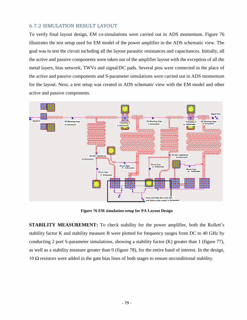
- 79 -
6.7.2 SIMULATION RESULT LAYOUT
To verify final layout design, EM co-simulations were carried out in ADS momentum. Figure 76
illustrates the test setup used for EM model of the power amplifier in the ADS schematic view. The
goal was to test the circuit including all the layout parasitic resistances and capacitances. Initially, all
the active and passive components were taken out of the amplifier layout with the exception of all the
metal layers, bias network, TWVs and signal/DC pads. Several pins were connected in the place of
the active and passive components and S-parameter simulations were carried out in ADS momentum
for the layout. Next, a test setup was created in ADS schematic view with the EM model and other
active and passive components.
Figure 76 EM simulation setup for PA Layout Design
STABILITY MEASUREMENT: To check stability for the power amplifier, both the Rollett’s
stability factor K and stability measure B were plotted for frequency ranges from DC to 40 GHz by
conducting 2 port S-parameter simulations, showing a stability factor (K) greater than 1 (figure 77),
as well as a stability measure greater than 0 (figure 78), for the entire band of interest. In the design,
10 Ω resistors were added in the gate bias lines of both stages to ensure unconditional stability.
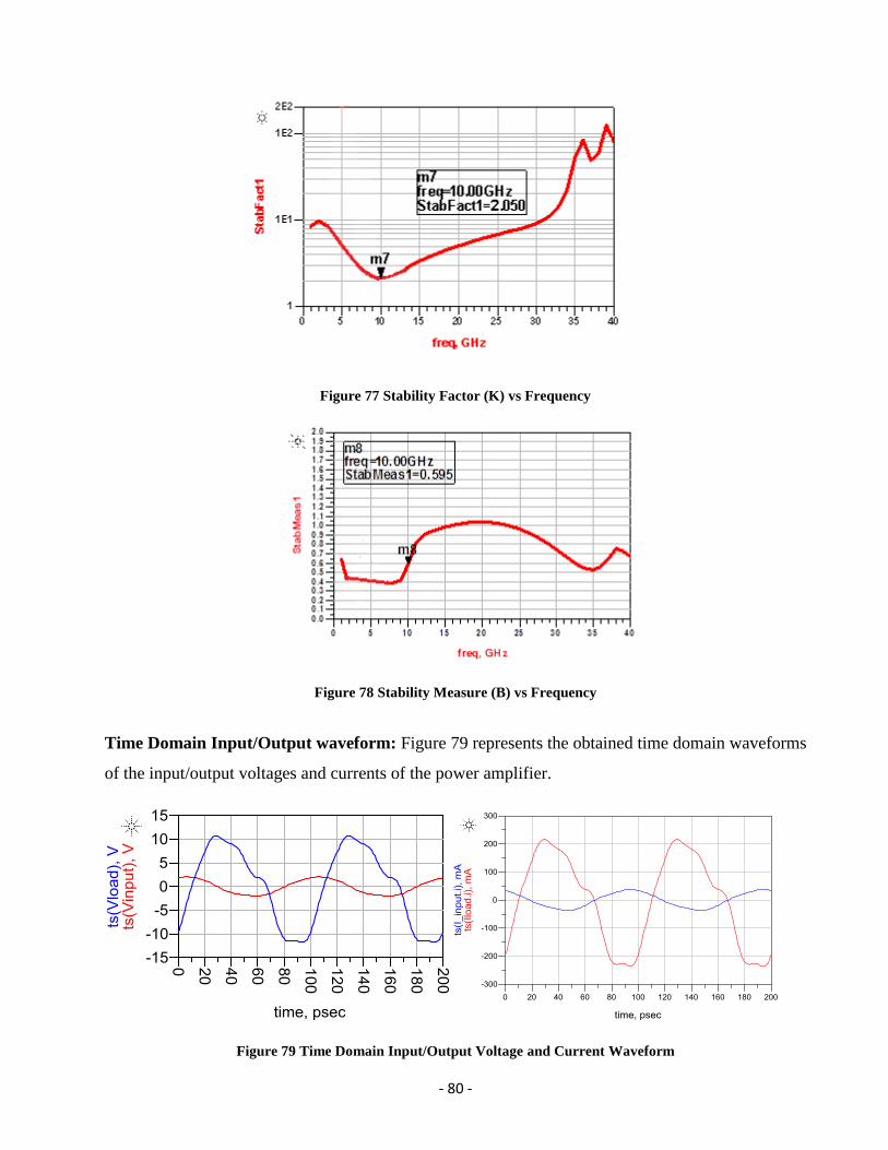
- 80 -
Figure 77 Stability Factor (K) vs Frequency
Figure 78 Stability Measure (B) vs Frequency
Time Domain Input/Output waveform: Figure 79 represents the obtained time domain waveforms
of the input/output voltages and currents of the power amplifier.
Figure 79 Time Domain Input/Output Voltage and Current Waveform
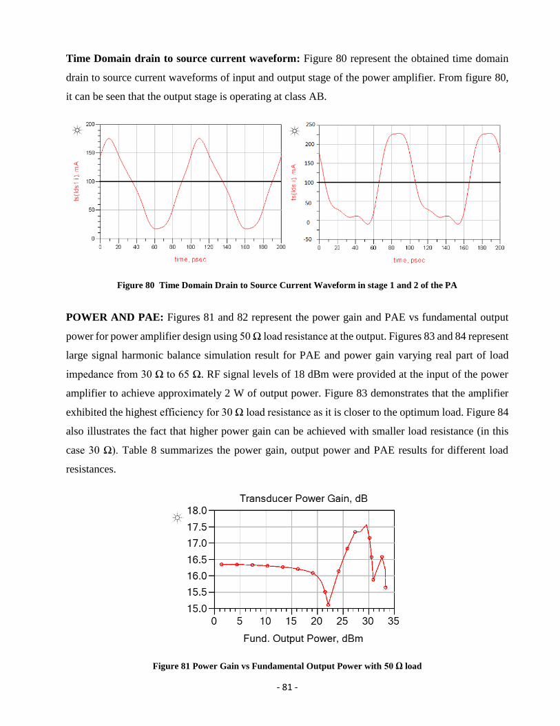
- 81 -
Time Domain drain to source current waveform: Figure 80 represent the obtained time domain
drain to source current waveforms of input and output stage of the power amplifier. From figure 80,
it can be seen that the output stage is operating at class AB.
Figure 80 Time Domain Drain to Source Current Waveform in stage 1 and 2 of the PA
POWER AND PAE: Figures 81 and 82 represent the power gain and PAE vs fundamental output
power for power amplifier design using 50 Ω load resistance at the output. Figures 83 and 84 represent
large signal harmonic balance simulation result for PAE and power gain varying real part of load
impedance from 30 Ω to 65 Ω. RF signal levels of 18 dBm were provided at the input of the power
amplifier to achieve approximately 2 W of output power. Figure 83 demonstrates that the amplifier
exhibited the highest efficiency for 30 Ω load resistance as it is closer to the optimum load. Figure 84
also illustrates the fact that higher power gain can be achieved with smaller load resistance (in this
case 30 Ω). Table 8 summarizes the power gain, output power and PAE results for different load
resistances.
Figure 81 Power Gain vs Fundamental Output Power with 50 Ω load

- 82 -
Figure 82 PAE vs Fundamental Output Power with 50 Ω load
Figure 83 PAE vs Load

- 83 -
Figure 84 Power Gain vs Load
Table 8 PA Result Summary @ 10 GHz (Input Power = 18 dBm)
LOAD (Ω) Output Power (dBm) PAE (%) Power Gain (dB)
30 35.38 33.18 17.38
35 34.98 32.58 16.98
40 34.18 31.50 16.18
45 33.87 30.69 15.87
50 33.60 29.90 15.60
55 33.35 29.15 15.35
60 33.11 28.41 15.11
65 32.88 27.68 14.88
Linearity: Large signal harmonic balance simulations with two fundamental tones were performed
for different output power levels in order to analyze the linearity performance of the power amplifier
for 10 GHz fundamental frequency with each frequency tone spaced by 0.01 GHz. Figures 85 and 86
show a 3rd order IMD tone of -32.39 dBc and 5th order IMD tone of -25 dBc when the output power
level is 28 dBm. From figure 87, the third order output referred IP3 (OIP3) was found to be 40 dBm
(IIP3 = 25 dBm), i.e., 7 dB higher than the maximum saturated output power level of the power
amplifier. The maximum saturated power of the amplifier design is approximately 33 dBm at 10 GHz.

- 84 -
Figure 85 High and Low Side 3rd Order IMD Tones vs Fundamental Output Power
Figure 86 High and Low Side 5th Order IMD Tones vs Fundamental Output Power
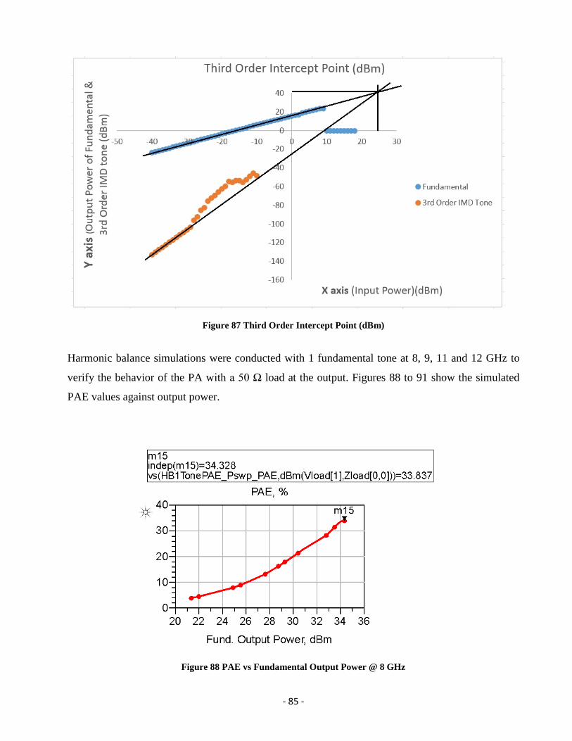
- 85 -
Figure 87 Third Order Intercept Point (dBm)
Harmonic balance simulations were conducted with 1 fundamental tone at 8, 9, 11 and 12 GHz to
verify the behavior of the PA with a 50 Ω load at the output. Figures 88 to 91 show the simulated
PAE values against output power.
Figure 88 PAE vs Fundamental Output Power @ 8 GHz
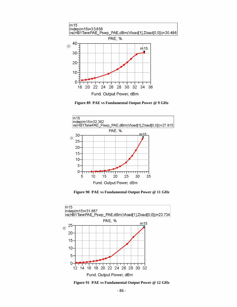
- 86 -
Figure 89 PAE vs Fundamental Output Power @ 9 GHz
Figure 90 PAE vs Fundamental Output Power @ 11 GHz
Figure 91 PAE vs Fundamental Output Power @ 12 GHz

- 87 -
The power amplifier exhibits the highest power added efficiency and output power at 8 GHz and the
lowest at 12 GHz fundamental frequency as expected. Table 9 summarizes the PA output power and
power added efficiency results from figures 88 to 91.
Table 9 Result Summary (Input Power = 18 dBm)
Frequency (GHz) Output Power (dBm) PAE (%)
8 34.33 33.84
9 33.86 30.50
11 32.38 27.60
12 31.69 23.73
6.8 DISCUSSIONS AND CONCLUSION
To the best of our knowledge, the proposed power amplifier is the first X band power amplifier to be
designed and fabricated using NRC’s GaN 150 kit to implement a 10 GHz TX/RX FEM. Whenever
possible, our results have been compared to commercial parts available and overall found to be very
competitive. As reported in Table 10, it can be first highlighted that the designed amplifier exhibits a
higher power added efficiency, thus expecting a competitive measured PAE vs. existing designs.
Results from literature feature a Ku-band amplifier, recently available from Qorvo and featuring their
0.15 µ process [73] with a power level of 34 dBm and efficiency of 25%. The power level obtained
in this work matches to this commercial chip and the power added efficiency exceeds than what they
have reported to a 50 Ω load at 2 W output power. Furthermore, this commercial chip uses 20 V drain
bias with 70 mA quiescent current while the proposed design uses 20 V with 90 mA quiescent current
but with a smaller die area, i.e., 2.026 x 0.849 mm2, in fact the smallest compared to the other designs
(Table 10). As for the third and fifth order IMD tones, it is respectively of -31 and -46 dBc at 24 dBm
output power for [71] and -32 and -25 dBc for 28 dBm output power in our design. It should be noted
that following the EM simulation results, the proposed PA can be used in point to point/multi point
communication like [69] - [72]. It can also be used as a PA driver for much higher power like in [73].

- 88 -
Table 10 PA PERFORMANCE COMPARISON WITH OTHER X\Ku BAND PAs
*: Commercial chip **: No on chip bias
TECHNOLOGY FREQUENCY
(GHz)
PEAK
PAE
(%)
POUT
(dBm)
OIP3
(dBm)
SIZE
(mm2)
DC
VOLTAGE
SUPPLY
GAIN
(dB)
REF
GaAs PHEMT 9-12 20 33 36 5 x 5
leadless
SMT
PACKAGE
7 20 [14]*
0.5 µm GaN
(FROM NRC)
0.5-6.5 38.1
@ 0.5
GHz
33.45
@ 0.5
GHz
>40 2x2** 15 > 10 [59]
0.8 µm GaN
8 4 28.1 -- -- 10 3.5 [66]
0.2 µm GaN
2-18 15 33
dBm
-- 4x2** 15 20 [67]
GaN HEMT 9.5-12 - 37.5
dBm
-- 3.5 X 2.8** 30 5.2 [68]
Triquint Power
PHEMT
10-12 29 34.5 43 5 x 5 x 0.85
6 25 [69]*
0.25 µm PHEMT 13-17 30 34 38 9.4x6.4x1.8 7 26 [70]*
0.25 µm PHEMT 6-18 20 34.5 -- -- 8 26 [71]*
Triquint Power
PHEMT
6-18 25 34.5 -- 4.445 x
3.023
8 24 [72]*
Qorvo’s 0.15um
GaN on SiC
13-18 25 33 --
1.25 X 2.1
die area
20 20 [73]*
NRC 0.15um
GaN on SiC
8-12 33 @
8
GHz
30@
10
GHz
34.5 @
8 GHz
33.362
@ 10
GHz
40 @
10
GHz
2.026 X
.849
20 16 This
work

- 89 -
CHAPTER 7 10 GHz FRONT-END DESIGN
The primary objective of this thesis was to integrate the designed low noise amplifier and power
amplifier with a GaN 0.15 µm switch to obtain a MMIC front-end module operating at 10 GHz and
have it fabricated. In this chapter, a wideband single pole single throw switch will be integrated with
the designed LNA and PA. Note that the design of the GaN Single Pole Double Throw (SPDT) switch
was completed by a fellow researcher from the ELEMENT research laboratory at the University of
Ottawa.
7.1 WIDEBAND SWITCH
The primary advantages of a fully integrated GaN transceiver front-end are its weight and size. As
explained in chapter 2, these two important parameters are substantially reduced by the use of
switches in the front-end architecture. This is partly accomplished by replacing the bulky and heavy
circulator with a SPDT switch, thus reducing the area of the RF front-end module significantly. The
use of GaN switches includes additional advantages such as improved linearity and power handling
capability of GaN. Due to GaN HEMT’s power survivability, the use of limiters can be reduced to
none which allows it to be smaller, cheaper, less power consuming and better system level front-end
architecture. [10] [21] – [23]
A broadband (2- 18 GHz) single pole double throw T/R switch has been then integrated with the LNA
and PA to achieve the 10 GHz front-end architecture. The final topology included a combination of
series/shunt switch sections to form the SPDT to ensure wideband performance. Figure 92 represents
a basic schematic diagram of a series/ shunt SPDT from ADS. The transistor model from the GaN
0.15 µm design kit by NRC was used as a core of the SPDT design. The sizes of switch transistors
were chosen to be 2 X 200 µm each as the ideal tradeoff between low insertion loss and high isolation.
The transistor “ON” and “OFF” voltages at the gate were optimized to achieve the minimum
respective resistance and capacitance from the required switch transistors.

- 90 -
Figure 92 Basic Series/Shunt SPDT Schematic
Figure 93 represents the layout of the shunt-series SPDT, which was integrated to achieve the front-
end module. The layout design of figure 93 uses four GaN HFET transistor layout models available
in the current version of GaN150v1.01 PDK.
Using the same guidelines as in this thesis, the transistors were oriented along the horizontal X
direction and placed as close as possible to achieve better small/large signal matching. In addition,
shorter signal line in between ensured the least possible path loss. The SPDT switch was implemented
in layout ensuring it was free of Design Rule Check (DRC) violations and subsequently submitted for
fabrication. The required DC blocking capacitors at the input/output signal path and shunt capacitors
were implemented using MIM capacitors available from the design kit. The SPDT layout design
required four 1.5 KΩ nichrome (NiCr) resistors to provide the “ON” and “OFF” voltages at the gate
of the four switch transistors and to increase RF isolation. In addition to keeping shorter length to
incur less path loss, the length and width of the signal lines in TX and RX path were varied to achieve
optimum matching in both sides of the switch and sufficient power handling capability in TX side, at
the same time complying with transmission line maximum current ratings for the required line widths.
Despite the differences in LNA and PA layout design length, the switch design in both TX and RX
chain was kept as symmetrical as possible.

- 91 -
Figure 93 Layout Design of SPDT (Area including pads 2.036 mm X 1.66 mm)
Figure 94 represents the overall layout driven schematic of the SPDT used in the FEM module. EM
simulations were conducted creating an EM model of the switch.
Figures 95 and 96 represent the EM simulation results for SPDT for TX and RX side. S-parameter
simulations were carried out to obtain insertion loss, isolation, and input/output return loss. The switch
transistors were turned ON with 0 V and turned off with -4.5 V at the gate of the transistors.
These figures demonstrate better than 10 dB input/output return loss from 2 GHz to 18 GHz
bandwidth for SPDT design. An Insertion loss of less than 1 dB was achieved for the entire band of
interest with isolation levels lower than -25 dB.
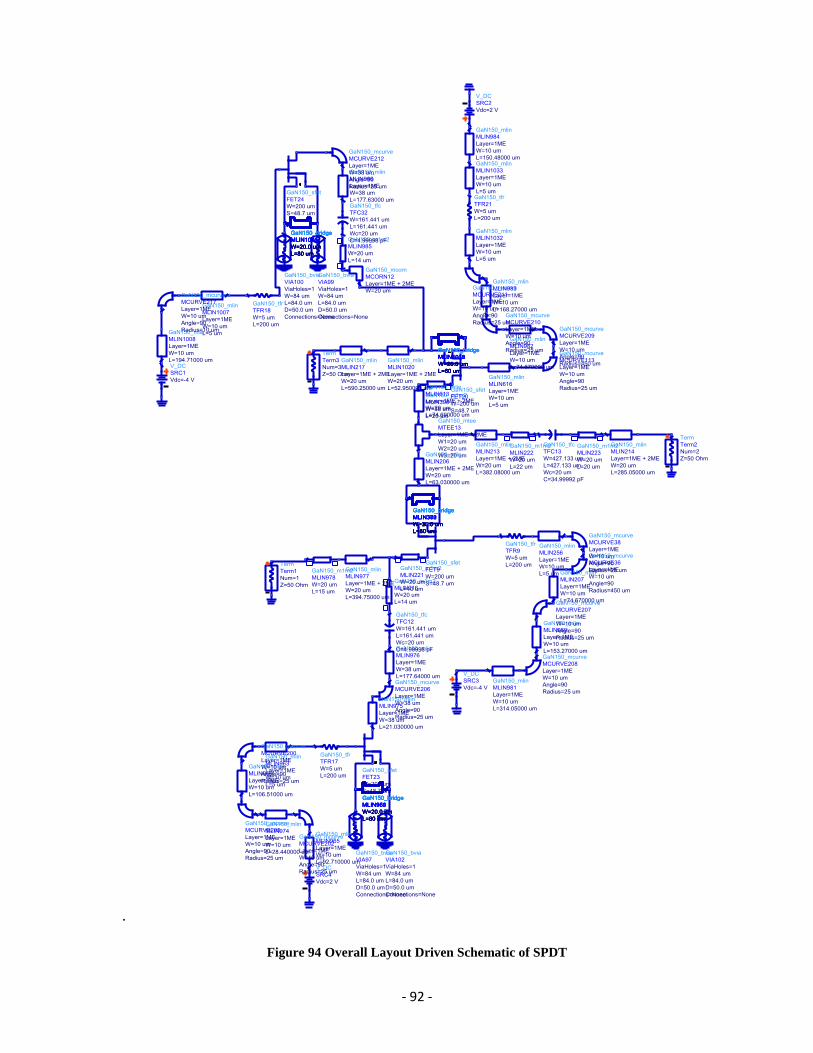
- 92 -
.
Figure 94 Overall Layout Driven Schematic of SPDT
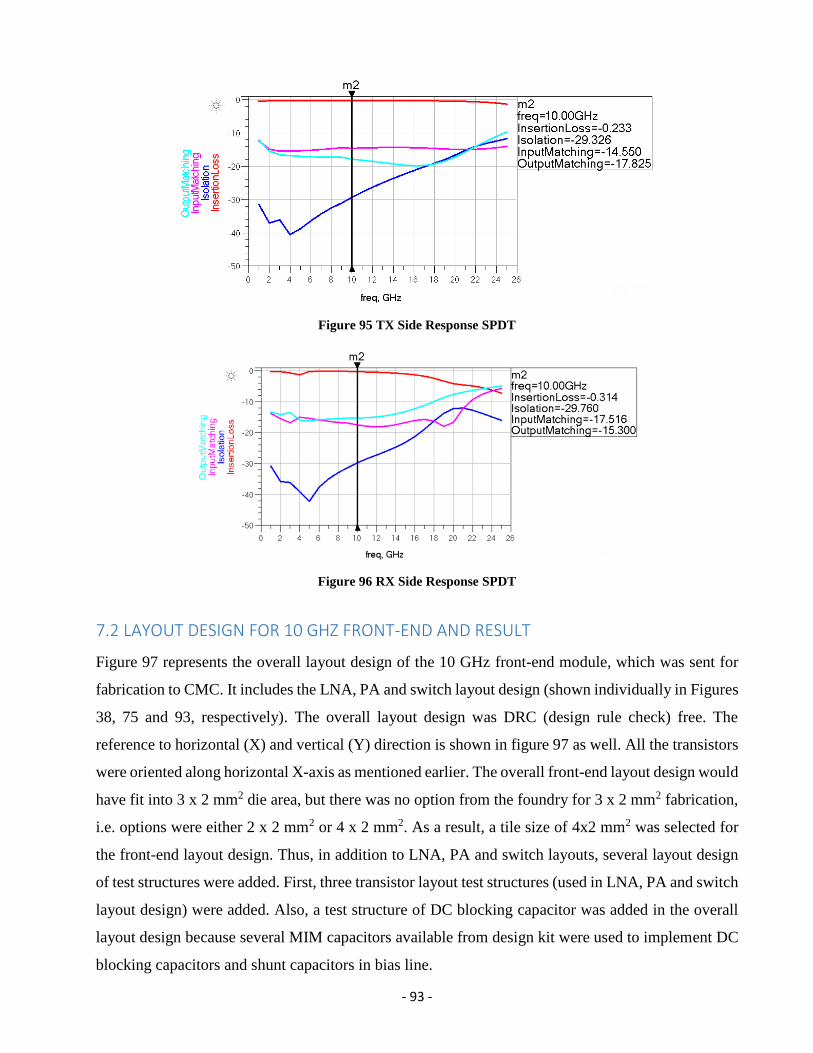
- 93 -
Figure 95 TX Side Response SPDT
Figure 96 RX Side Response SPDT
7.2 LAYOUT DESIGN FOR 10 GHZ FRONT-END AND RESULT
Figure 97 represents the overall layout design of the 10 GHz front-end module, which was sent for
fabrication to CMC. It includes the LNA, PA and switch layout design (shown individually in Figures
38, 75 and 93, respectively). The overall layout design was DRC (design rule check) free. The
reference to horizontal (X) and vertical (Y) direction is shown in figure 97 as well. All the transistors
were oriented along horizontal X-axis as mentioned earlier. The overall front-end layout design would
have fit into 3 x 2 mm2 die area, but there was no option from the foundry for 3 x 2 mm2 fabrication,
i.e. options were either 2 x 2 mm2 or 4 x 2 mm2. As a result, a tile size of 4x2 mm2 was selected for
the front-end layout design. Thus, in addition to LNA, PA and switch layouts, several layout design
of test structures were added. First, three transistor layout test structures (used in LNA, PA and switch
layout design) were added. Also, a test structure of DC blocking capacitor was added in the overall
layout design because several MIM capacitors available from design kit were used to implement DC
blocking capacitors and shunt capacitors in bias line.
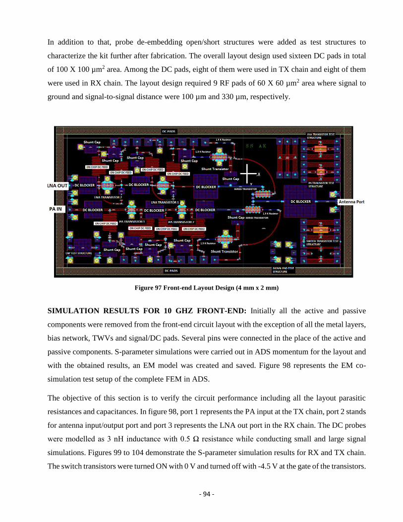
- 94 -
In addition to that, probe de-embedding open/short structures were added as test structures to
characterize the kit further after fabrication. The overall layout design used sixteen DC pads in total
of 100 X 100 µm2 area. Among the DC pads, eight of them were used in TX chain and eight of them
were used in RX chain. The layout design required 9 RF pads of 60 X 60 µm2 area where signal to
ground and signal-to-signal distance were 100 µm and 330 µm, respectively.
Figure 97 Front-end Layout Design (4 mm x 2 mm)
SIMULATION RESULTS FOR 10 GHZ FRONT-END: Initially all the active and passive
components were removed from the front-end circuit layout with the exception of all the metal layers,
bias network, TWVs and signal/DC pads. Several pins were connected in the place of the active and
passive components. S-parameter simulations were carried out in ADS momentum for the layout and
with the obtained results, an EM model was created and saved. Figure 98 represents the EM co-
simulation test setup of the complete FEM in ADS.
The objective of this section is to verify the circuit performance including all the layout parasitic
resistances and capacitances. In figure 98, port 1 represents the PA input at the TX chain, port 2 stands
for antenna input/output port and port 3 represents the LNA out port in the RX chain. The DC probes
were modelled as 3 nH inductance with 0.5 Ω resistance while conducting small and large signal
simulations. Figures 99 to 104 demonstrate the S-parameter simulation results for RX and TX chain.
The switch transistors were turned ON with 0 V and turned off with -4.5 V at the gate of the transistors.
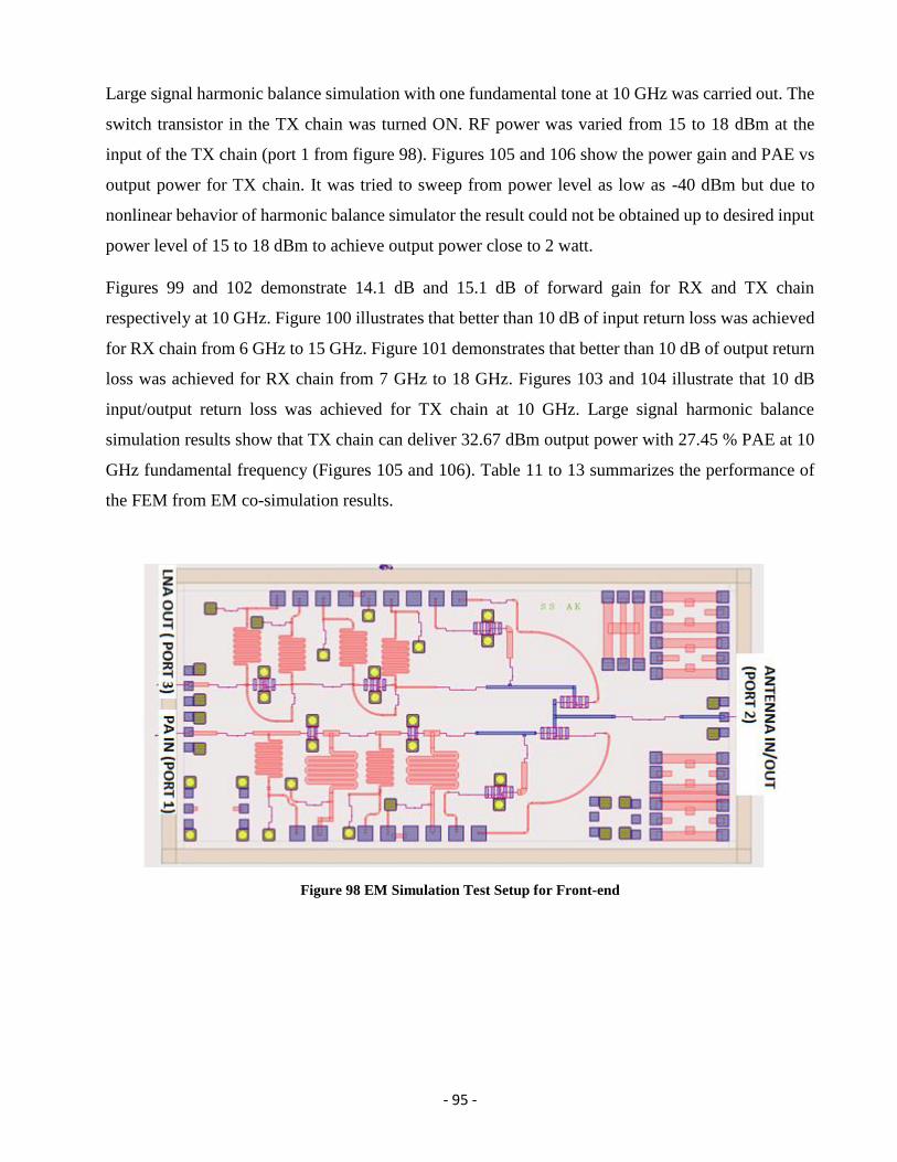
- 95 -
Large signal harmonic balance simulation with one fundamental tone at 10 GHz was carried out. The
switch transistor in the TX chain was turned ON. RF power was varied from 15 to 18 dBm at the
input of the TX chain (port 1 from figure 98). Figures 105 and 106 show the power gain and PAE vs
output power for TX chain. It was tried to sweep from power level as low as -40 dBm but due to
nonlinear behavior of harmonic balance simulator the result could not be obtained up to desired input
power level of 15 to 18 dBm to achieve output power close to 2 watt.
Figures 99 and 102 demonstrate 14.1 dB and 15.1 dB of forward gain for RX and TX chain
respectively at 10 GHz. Figure 100 illustrates that better than 10 dB of input return loss was achieved
for RX chain from 6 GHz to 15 GHz. Figure 101 demonstrates that better than 10 dB of output return
loss was achieved for RX chain from 7 GHz to 18 GHz. Figures 103 and 104 illustrate that 10 dB
input/output return loss was achieved for TX chain at 10 GHz. Large signal harmonic balance
simulation results show that TX chain can deliver 32.67 dBm output power with 27.45 % PAE at 10
GHz fundamental frequency (Figures 105 and 106). Table 11 to 13 summarizes the performance of
the FEM from EM co-simulation results.
Figure 98 EM Simulation Test Setup for Front-end

- 96 -
Figure 99 Forward Gain vs Frequency of the RX Chain
Figure 100 Input Return Loss vs Frequency of the RX Chain
Figure 101 Output Return Loss vs Frequency RX Chain
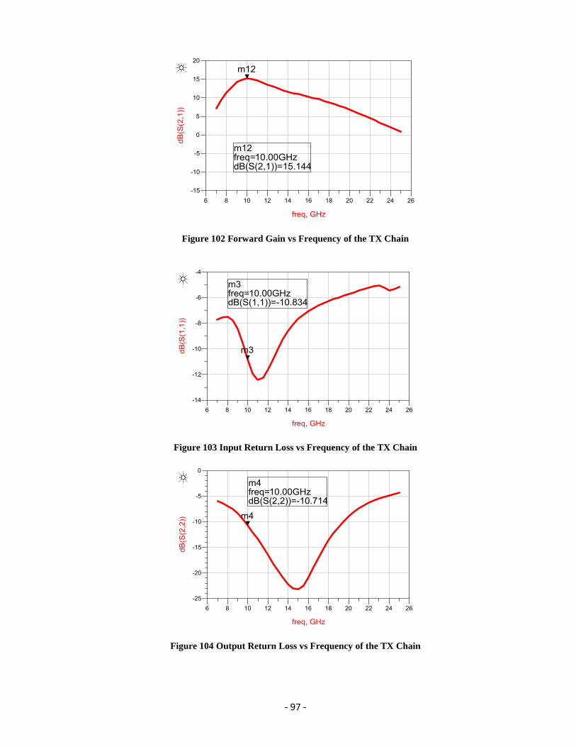
- 97 -
Figure 102 Forward Gain vs Frequency of the TX Chain
Figure 103 Input Return Loss vs Frequency of the TX Chain
Figure 104 Output Return Loss vs Frequency of the TX Chain

- 98 -
Figure 105 Power Gain vs Output Power TX Chain
Figure 106 PAE vs Output Power TX Chain
7.3 DISCUSSIONS AND CONCLUSION
In this Chapter, the performance of a fully integrated 10 GHz FEM making use of a novel 0.15um
process from NRC has been demonstrated. Results agree with initial system specifications and show
the competitive edge of this design when compared to other results in the literature as well as
commercially available parts. Design was submitted to foundry and currently in fabrication. Testing
of the FEM will be completed once fabrication is complete.

- 99 -
Table 11 RX CHAIN PERFORMANCE SUMMARY
PARAMETERS LNA SWITCH RX CHAIN
Forward Gain, S21 ≥ 12 dB
for 7 GHz − 15 GHz
INSERTION LOSS ≤
1 dB
(2 GHz – 18 GHz)
≥ 𝟏𝟐 𝐝𝐁
𝐟𝐨𝐫 𝟕 𝐆𝐇𝐳 − 𝟏𝟒 𝐆𝐇𝐳
Input matching, S11
(dB)
≤-10 dB (6 GHz to 14
GHz)
≤-10 dB (2 GHz to 18
GHz)
≤-10 dB (7 GHz to 15
GHz)
Output matching, S22
(dB)
≤-10 dB (3.8 GHz to 15.5
GHz)
≤-10 dB (2 GHz to 18
GHz)
≤-10 dB (7 GHz to 18
GHz)
Table 12 TX CHAIN PERFORMANCE SUMMARY (Input = 18 dBm)
PARAMETERS PA TX CHAIN
OUTPUT POWER 33.60 dBm 32.67 dBm
POWER GAIN 15.60 dB 14.67 dB
PAE 29.90 % 27.45 %
Table 13 FEM POWER CONSUMPTION
SINGLE DC
SUPPLY
VOLTAGE
SUPPLY
QUIESCENT
DRAIN CURRENT
For RX CHAIN
SUPPLY
QUIESCENT
DRAIN CURRENT
For TX CHAIN
20 V 80 mA
180 mA
- 100 -
CHAPTER 8 CONCLUSION AND FUTURE WORK
8.1 CONCLUSION
In this thesis, a low noise amplifier and a power amplifier for X band were designed using a novel
GaN 0.15µm technology on silicon carbide wafer provided by NRC. In addition, a GaN 0.15µm
single-pole-double-throw (SPDT) switch was integrated with the designed amplifiers to achieve a RF
front-end architecture for X band.
This work offers multiple inspiring research opportunities towards the implementation of future front-
end solutions in next generation of military, aerospace, and civil wireless communication systems as
well as in biomedical applications as it can reduce size, provide high power with high efficiency, low
noise, high linearity, and robustness for applications in harsh environments.
The low noise amplifier and power amplifier designed and reported in this thesis have demonstrated
the feasibility of achieving wideband, efficient and smaller front-end module design using NRC’s
GaN 0.15 µm process. The obtained performance for both amplifiers can be successfully compared
to other existing X band LNA and PA designs.
As for the LNA, it should be noted that in the absence of noise model from the foundry, this work
extrapolated a current density of 0.15 (ID/IDSS) as the optimum bias point used for lowest noise figure
based on values reported in GaAs and experimental values for GaN [46]. The designed low noise
amplifier demonstrated, in simulations, one of the best input/output return loss compared to existing
X band low noise amplifiers. The EM simulation results of designed LNA demonstrated input return
loss better than 20 dB from 7 GHz to 11 GHz and output return loss better than 20 dB from 5 GHz to
12 GHz. The forward gain achieved was more than 12 dB from 7 GHz to 15 GHz with a maximum
gain of 14.69 dB at 10 GHz. This design represents the first attempt to implement a full integrated X
band FEM using a novel 0.15um GaN process from NRC. In the future, the obtained results can be
further improved with the addition of noise models from the foundry.
In addition, the power amplifier shows acceptable results for power and efficiency for the overall X
band frequency range. In the lower end of the X band range (i.e., 8 GHz), the PA delivers 34.33 dBm
of output power with 33.84 % PAE. At 12 GHz, it was shown to deliver 31.69 dBm power with 23.73
% PAE to a 50 Ω load. At the desired center frequency of 10 GHz, it delivers 33.6 dBm power with
29.9 % PAE to a 50 Ω load.
- 101 -
Compared to other power amplifiers operating at similar frequency range and linearity requirement,
the proposed amplifier exhibits one of the highest power added efficiencies. Note that optimum load
can be provided off chip to further increase the power added efficiency.
It is also noteworthy to mention that the designed LNA and PA required one of the smallest die areas
including the quarter wave length DC bias network and blocking capacitors when compared to other
X band LNAs and PAs with similar design specifications. The LNA and PA were integrated with a
wide band SPDT to form a 10 GHz front-end design. The simulation results of the front-end module
demonstrate a good small signal gain and input/output return loss in TX and RX chain with 27.45 %
efficiency delivering approximately 2 W power to a 50 Ω load.
8.2 FUTURE WORK
The front-end module chip designed in this manuscript has recently been received from foundry after
fabrication. Measurement of this front-end module chip will be the first task planned in the near future.
It should be noted, this was the first scheduled fabrication run for this process.
Input impedance and antenna radiation pattern changes due to the detuning effects from changes in
operational and environmental conditions. The fellow researcher who designed the switch also
worked on an impedance tuner circuit on GaN150 process. The layout design of the impedance tuner
circuit can be integrated with the power amplifier layout designed in this thesis to address detuning
effects. After the impedance tuner circuit will be integrated, the power amplifier response can be
further analyzed in the presence of a variable load presented by an antenna with the output matching
network due to the change of environmental condition and detuning effects. In addition to this, thermal
performance of the PA design can be characterized and the correlation between temperature and RF
performance can be presented. Also, noise data can be collected and used to develop a reliable noise
model of this device.
In addition to that, system level simulation such as envelope simulation can be conducted using
different modulation techniques to further characterize the PA behavior verifying EVM and ACLR.
The designed PA was a class AB power amplifier. However, switch mode power amplifier (E/F) can
be considered to increase efficiency. If the goal is more toward linearization rather efficiency
enhancement, digital pre-distortion linearization technique can also be practiced.
- 102 -
REFERENCES
[1] E. Dahlman et al. (2014). “5G Radio Access.” [Online]. Available:
http://www.ericsson.com/res/thecompany/docs/publications/ericsson_review/2014/er-5g-
radio-access.pdf [Dec. 7, 2015]
[2] T. Parker. (2014). “FierceWirelessTech.” [Online]. Available:
http://www.fiercewireless.com/tech/story/ericsson-5g-will-require-lots-new-spectrum-above-
10-ghz/2014-07-16 [Dec. 7, 2015]
[3] D. Flore. (2015). “3GPP.” [Online]. Available: http://www.3gpp.org/news-events/3gpp-
news/1674-timeline_5g [Dec. 7, 2015]
[4] M. Feng, S. Shyh-Chiang, D.C. Caruth, and J.-J. Huang, “Device technologies for RF front-end
circuits in next-generation wireless communications.” Proc. IEEE, vol. 92, pp. 354-375, Feb
2004
[5] 4G Americas. (2014). “Wireless Handset RF Front-End Optimization.” [Online]. Available:
http://www.4gamericas.org/files/3114/1323/4646/4GA_RFFE_Optimization_Oct_2014.pdf
[Dec. 7, 2015]
[6] 4G Americas. (2014). “4G Mobile Broadband Evaluation 3GPP Release 11 & Release 12 and
Beyond.” [Online]. Available:
http://www.4gamericas.org/files/2614/0758/7473/4G_Mobile_Broadband_Evolution_Rel-
11__Rel_12_and_Beyond_Feb_2014_-_FINAL_v2.pdf [Dec. 7, 2015]
[7] W-CDMA Super-Heterodyne Reference Design: V1.0 RF Transceiver Description, Maxim-
Dallas Semiconductor, 2001.
[8] T.C. Cheung, “2 GHz W-CDMA radio transceiver,” M.S. thesis, Virginia Tech. Univ.,
Blacksburg, VA, 1998.
[9] J. S. Love, RF Front-End World Class Designs, Burlington: MA, Newnes, 2009.
[10] M. Thorsell et al., “An X-Band AlGaN/GaN MMIC Receiver Front-End.” IEEE Microwave
and Wireless Components Letters, vol. 20, pp. 55-57, Nov. 2009.
[11] S. Masuda et al., “GaN single-chip transceiver frontend MMIC for X-Band
applications,” IEEE-MTT Microwave Symp. Digest, pp. 1-3, Montreal, Canada, June 2012.
[12] F.H. Raab et al., “Power amplifiers and transmitters for RF and microwave,” IEEE Trans.
Microwave Theory Tech, vol. 50, pp. 814-826, March 2002.
[13] Wikipedia. (2015). “X band,”[Online]. Available: https://en.wikipedia.org/wiki/X_band [Dec.
7, 2015]

- 103 -
[14] Analog Devices. (2015). “HMC487LP5 / HMC487LP5E Datasheet.” [Online]. Available:
https://www.hittite.com/products/view.html/view/HMC487LP5 [Dec. 7, 2015]
[15] J.P.B. Janssen et al., “Robust X-band LNAs in AlGaN/GaN technology,” European Microwave
Integrated Circuits Conf., pp. 101-104, Rome, Italy, Sept. 2009.
[16] J.W.M. Rogers and C. Plett, Radio Frequency Integrated Circuit Design, Norwood: MA, Artech
House, 2003.
[17] A. Abuelmaatti, “RF techniques for IEEE 802.15.4: circuit design and device modelling,” Ph.D.
dissertation, University of Glasgow, U.K., 2008.
[18] National Research Council Canada, “Gallium Nitride MMIC Foundry Design Manual, GaN150
Version 1.01,” Release date: February 9, 2015.
[19] N. Billstrom, J. Nilsson, A. Tengs, and N. Rorsman, “High performance GaN frontend
MMICs,” European Microwave Integrated Circuits Conf., pp. 348-351, Manchester, U.K., Oct.
2011.
[20] B. Razavi, RF Microelectronics, Upper Saddle River: NJ, Prentice Hall, 1998.
[21] M. Rudolph et al., “Analysis of the survivability of GaN low-noise amplifiers”, IEEE Trans.
Microwave Theory Tech., vol. 55, pp. 37-43, Jan. 2007.
[22] J.P.B. Janssen et al., “X-band robust AlGaN/GaN receiver MMICs with over 41 dBm power
handling,” IEEE Compound Semiconductor IC Symp., pp. 1-4, Monterey, CA, Oct. 2008.
[23] P. Schuh et al., “GaN MMIC based T/R-module front-end for X band applications,” European
Microwave Integrated Circuits Conf., pp. 274-277, Amsterdam, The Netherlands, Oct. 2008.
[24] A. Litwin, O. Bengtsson, and J. Olsson, “Novel BiCMOS compatible, short channel LDMOS
technology for medium voltage RF and power applications,” IEEE MTT-S Microwave Symp.
Digest, pp. 35–38, Seattle, WA, June 2002.
[25] “HF Transistors.”[Online]. Available: www.cambridge.org/ca/download_file/217993 [Dec. 7,
2015]
[26] C.-K. Liu and Y.-H. Cheng, “Thermal analysis of power amplifier package in cellular
phones,” Proc. of the 4th Int. Symp. on Electronic Materials and Packaging, pp. 415-
421, Kaohsiung, Taiwan, 4-6 Dec. 2002
[27] Microwaves101. (2013). “Efficiency.” [Online]. Available:
http://www.microwaves101.com/encyclopedia/efficiency.cfm [Dec. 7, 2015]
[28] L. Baragiola, M. Frigerio, B. Gabbrielli, and A. Panzeri, “Improvement of power efficiency and
cost reduction solution in microwave linear power amplifier,” European Microwave Integrated
Circuits Conf., pp. 1321-1324, Amsterdam, The Netherlands, Oct. 2004.
- 104 -
[29] C.E. Weitzel, “RF power devices for wireless communications,” IEEE MTT-S Microwave
Symp. Digest, pp. 285-288, Seattle, WA, June 2002.
[30] R.S. Pengelly et al., “A review of GaN on SiC High electron-mobility power transistors and
MMICs,” IEEE Trans. Microwave Theory Tech., vol. 60, no.6, pp. 1764-1783, June 2012.
[31] Y.-F. Wu et al., “Very-high power density AlGaN/GaN HEMTs,” IEEE Trans. Elect. Devices,
vol. 48, no. 3, pp. 586-590, Mar. 2001.
[32] S.C. Binari et al., “Trapping effects and microwave power performance in AlGaN/GaN
HEMTs,” IEEE Trans. Elect. Devices, vol. 48, pp. 465-471, Mar. 2001.
[33] D. Pavlidis, P. Valizadeh, and S.H. Hsu, “AlGaN/GaN high electron mobility transistor
(HEMT) reliability,” European Gallium Arsenide and Other Semiconductors Application
Symp., pp. 265-268, Paris, Oct. 2005.
[34] J. M. Golio, RF and Microwave Semiconductor Device Handbook, Boca Raton: FL, CRC Press,
2003
[35] R. Quay, Gallium Nitride Electronics, Freiburg: Germany, Springer, 2008
[36] S. Islam and A.F.M. Anwar, “Self-heating and trapping effects on the RF performance of GaN
MESFETs,” IEEE Trans. Microwave Theory Tech., vol. 52, no. 4, pp. 1229-1236, April 2004
[37] D. M. Pozar, Microwave engineering, NJ, JohnWiley & Sons, 2012.
[38] P. Sharma, “Design of a 3.1-4.8 GHz RF-front-end for an ultra-wideband receiver,” M.S. thesis,
Univ. Texas, TX, 2005.
[39] S. Lee, K.J. Webb, V. Tilak, and L.F. Eastman, “Intrinsic noise equivalent-circuit parameters
for AlGaN/GaN HEMTs,” IEEE Trans. Microwave Theory Tech., vol. 51, no. 5, pp. 1567-1577,
May 2003.
[40] A.V. Vertiatchikh and L.F. Eastman, “Effect of the surface and barrier defects on the
AlGaN/GaN HEMT low-frequency noise performance,” IEEE Trans. Elect. Devices, vol. 24,
no. 9, pp. 535-537, Sept. 2003.
[41] K.W. Kobayashi et al., “A 2 watt, Sub-dB Noise Figure GaN MMIC LNA-PA amplifier with
multi octave bandwidth from 0.2–8 GHz” IEEE MTT-S Microwave Symp. Digest, pp. 619-622,
Honolulu, HI, June 2007.
[42] S.B.T. Wang, A.M. Niknejad, and R.W. Brodersen, “Design of a Sub-mW 960-MHz UWB
CMOS LNA,” IEEE J. Solid-State Circuits, vol. 41, pp. 2449-2456, Nov. 2006.
[43] U. Mishra, S. Likun, T. Kazior, and Y.-F. Wu, “GaN-based RF power devices and amplifiers,”
Proc. IEEE, vol. 96, no. 2, pp. 287–305, Feb. 2008.

- 105 -
[44] Aethercomm.”Gallium Nitride (GaN) microwave transistor technology for radar application.”
[Online]. Available: http://www.aethercomm.com/articles/9.pdf [Dec. 7, 2015]
[45] K.W. Kobayashi et al. (2012). “GaN Low Noise Broadband Amplifiers and Technology.”
[Online]. Available:
http://citeseerx.ist.psu.edu/viewdoc/download?doi=10.1.1.364.6164&rep=rep1&type=pdf
[Dec. 7, 2015]
[46] A. Bettidi et al., “X-Band GaN-HEMT LNA performance versus robustness trade-off,”
European Microwave Integrated Circuits Conf., pp. 1792-1795, Rome, Italy, Sept. 2009.
[47] L. Ulrich et al., “Highly Linear X-band GaN-based low-noise amplifier,” Int. Symp. on Signals,
Systems and Electronics, pp. 1-4, Potsdam, Germany, Oct. 2012.
[48] M. Micovic et al., “Robust broadband (4 GHz–16 GHz) GaN MMIC LNA,” IEEE Compound
Semiconductor IC Symp., pp. 1–4, Portland, OR, Oct. 2007.
[49] D. Krausse et al., “Robust GaN HEMT low-noise amplifier MMICs for X-Band applications,”
European Gallium Arsenide and Other Semiconductors Application Symp, Amsterdam, The
Netherlands, pp. 71-74, Sept. 2004.
[50] J.P.B. Janssen et al., “Robust X-band LNAs in AlGaN/GaN technology,” European Microwave
Integrated Circuits Conf., pp. 101-104, Rome, Italy, Sept. 2009
[51] RFMD+TriQuint=Qorvo. (2015). “TGA227 Datasheet.” [Online]. Available:
http://www.triquint.com/products/p/TGA227. [Dec. 7, 2015]
[52] RFMD+TriQuint=Qorvo. (2015). “TGA2511 Datasheet.” [Online]. Available:
http://http://www.triquint.com/products/p/TGA2511. [Dec. 7, 2015]
[53] RFMD+TriQuint=Qorvo. (2015). “TGA2512 Datasheet.” [Online]. Available:
http://www.triquint.com/products/p/TGA2512. [Dec. 7, 2015]
[54] T.H. Lee, “The design of CMOS Radio-Frequency integrated circuits, 2nd edition,”
Communications Engineer, vol. 2, pp. 47, Sept. 2004.
[55] K.B. Niclas, “GaAs MESFET feedback amplifier. Design consideration and characteristics,”
IEEE Trans. Microwave Theory Tech., pp. 39-40, Mar. 1980.
[56] K.B. Niclas, “The matched feedback amplifier: Ultrawide-band microwave amplification with
GaAs MESFET’s,” IEEE Trans. Microwave Theory Tech., vol. 28, pp. 285-294, Apr. 1980.
[57] S.-S. Bor et al., “Using feedback techniques to design a stable and matching condition for
microwave transistor amplifiers,” Int. J. Electronics, vol. 81, no. 6, pp. 713-721, Apr. 1996.
- 106 -
[58] F. Perez and V. Ortega, “A graphical method for the design of feedback networks for microwave
transistor amplifiers: theory and applications”, IEEE Trans. Microwave theory Tech., vol. 29,
no. 10, pp. 1019-1026, Oct. 1981.
[59] X. Zhou, “A highly efficient, linear and broadband GaN MMIC power amplifier,” M.S. thesis,
Carleton. Univ., Ottawa, Canada, 2012.
[60] M.C.E. Yagoub, Lecture Notes ELG 6369 : Nonlinear Microwave Devices and Effects, Faculty
of Engineering, University of Ottawa, Ottawa, ON, Canada.
[61] I. Rosu. “LNA Design.” [Online]. Available: http://www.qsl.net/va3iul/LNA%20design.pdf
[Dec. 7, 2015]
[62] I. Rosu. “RF Power Amplifiers.” [Online]. Available: http://www.qsl.net/va3iul [Dec. 7, 2015]
[63] V. Viswanathan, “Efficiency enhancement of base station power amplifiers using Doherty
technique,” M.S thesis, Virginia Polytechnic Institute and State Univ., Virginia, 2004
[64] C. DeMartino. (2013, October). “Power Amplifier Technology Targets Efficiency.” [Online].
Available: http://mwrf.com/semiconductors/power-amplifier-technology-targets-efficiency
[Dec. 7, 2015]
[65] Microwaves101. (2013), “Efficiency.” [Online]. Available:
http://www.microwaves101.com/encyclopedia/efficiency.cfm [Dec. 7, 2015]
[66] M. Li and R.E. Amaya, “A high-frequency power amplifier using GaN power cell technology”
Wireless and Microwave Tech. Conf., pp. 1-5, Melbourne, FL, April 2010
[67] R. Santhakumar et al., “Two stage high gain high-power distributed amplifier using dual-gate
GaN HEMTS,” IEEE Trans. Microwave Theory Tech., vol. 59, pp. 2059-2063, Aug 2011.
[68] E.M. Suijker et al., “GaN MMIC power amplifier for S-band and X-band,” European
Microwave Integrated Circuits Conf., pp. 297-300, Amsterdam, The Netherlands, Oct. 2008
[69] RFMD+TriQuint=Qorvo. (2015). “TGA2525-SM Datasheet.” [Online]. Available:
http://www.triquint.com/products/p/TGA2535-SM [Dec. 7, 2015]
[70] RFMD+TriQuint=Qorvo. (2015). “TGA2902-1-SCC-SG Datasheet.” [Online]. Available:
http://www.triquint.com/products/p/TGA2902-1-SCC-SG [Dec. 7, 2015]
[71] RFMD+TriQuint=Qorvo. (2015). “TGA2501-GSG Datasheet.” [Online].Available:
http://www.triquint.com/products/p/TGA2501-GSG [Dec. 7, 2015]
[72] RFMD+TriQuint=Qorvo. (2015). “TGA2501-TS Datasheet.” [Online]. Available:
http://www.triquint.com/products/p/TGA2501-TS [Dec. 7, 2015]
[73] RFMD+TriQuint=Qorvo. (2015). “TGA2958SM Datasheet.” [Online]. Available:
http://www.rfmw.com/ProductDetail/TGA2958SM-Qorvo-TriQuint/572959/ [Dec. 7, 2015]