Embed Size (px)
Citation preview

STB
Digital TVDVD Player
TMDS2512-to-1
PHY SX
TMDS251
www.ti.com SLLS852A –AUGUST 2007–REVISED JULY 2011
2.5 Gbps 2-TO-1 DVI/HDMI SWITCHCheck for Samples: TMDS251
• 3.3-V Fixed Supply to TMDS I/Os1FEATURES
• 5-V Fixed Supply to HPD, DDC, and Source• Compatible with HDMI 1.3aSelection Circuits• Supports 2.5 Gbps Signaling Rate for 480i/p,
• 64-Pin TQFP Package720i/p, and 1080i/p Resolutions up to 12-Bit• Footprint Compatible with 3-to-1 SwitchColor Depth
TMDS351 with Port 3 Disabled• Integrated Switchable Receiver Termination• ROHS Compatible and 260°C Reflow Rated• Selectable Receiver Equalization to• TMDS250 is Available with Port 1 Disabled andAccommodate to Different Input Cable
Ports 2 and 3 EnabledLengths• Supports 5-V to 3.3-V Level Shifting on DDC• Intra-Pair Skew < 40 ps
Links• Inter-Pair Skew < 65 ps• HBM ESD Protection Exceeds 8 kV to TMDS
APPLICATIONSInputs• Digital TV• Digital Projector
DESCRIPTIONThe TMDS251 is a 2-port digital video interface (DVI) or high-definition multimedia interface (HDMI) switch thatallows up to 2 DVI or HDMI ports to be switched to a single display terminal. Four TMDS channels, one hot plugdetector, and a digital display control (DDC) interface are supported on each port. Each TMDS channel supportssignaling rates up to 2.5 Gbps to allow 1080p resolution in 12-bit color depth.
The input port is enabled by configuring source selectors, S1 and S2. When an input port is selected, the TMDSinputs are connected to the TMDS outputs through a 2-to-1 multiplexer, the MOSFET between the input DDCchannel and the output DDC channel is turned on, and the HPD output follows the state of the HPD_SINK. Theother input port is inactive with disconnected input terminations, disconnected TMDS inputs to the outputs,disconnected DDC inputs to the outputs, and the HPD outputs are low state. Check the source selection look uptable for the details of port selections.
When S1 is high and S2 is low, all input terminations are disconnected, TMDS inputs are high impedance withstandard TMDS terminations, all internal MOSFETs are turned off to disable the DDC links, and all HPD outputsare connected to the HPD_SINK. This allows the initiation of the HDMI physical address discovery process.
Termination resistors (50-Ω), pulled up to VCC, are integrated at each TMDS receiver input. External terminationsare not required. A precision resistor is connected externally from the VSADJ pin to ground for setting thedifferential output voltage to be compliant with the TMDS standard.
Typical Application
1
Please be aware that an important notice concerning availability, standard warranty, and use in critical applications of TexasInstruments semiconductor products and disclaimers thereto appears at the end of this data sheet.
PRODUCTION DATA information is current as of publication date. Copyright © 2007–2011, Texas Instruments IncorporatedProducts conform to specifications per the terms of the TexasInstruments standard warranty. Production processing does notnecessarily include testing of all parameters.

TMDS251
SLLS852A –AUGUST 2007–REVISED JULY 2011 www.ti.com
These devices have limited built-in ESD protection. The leads should be shorted together or the device placed in conductive foamduring storage or handling to prevent electrostatic damage to the MOS gates.
DESCRIPTION CONTINUEDThe TMDS251 provides two levels of receiver input equalization for different ranges of cable lengths. EachTMDS receiver owns frequency responsive equalization circuits. When EQ sets low, the receiver supports theinput connection in short range HDMI cables. When EQ sets high, the receiver supports the input connection inlong range HDMI cables. The TMDS251 supports power saving operation. When a system is under standbymode and there is no digital audio/visual content from a connected source, the 3.3-V supply voltage, VCC, can bepowered off to minimize power consumption from the TMDS inputs, outputs, and internal switching circuits. TheHPD, DDC, and source selection circuits are powered up by the 5-V supply voltage, VDD, to maintain the systemhot plug detect response, the DDC link from the selected source to the sink under system standby operation. Thedevice is characterized for operation from 0°C to 70°C.
2 Copyright © 2007–2011, Texas Instruments Incorporated

SCL_SINK
SDA_SINK
HPD_SINK
S1
S2ControlLogic
Y4
Z4
VSADJ
TMDSDriver
TMDSDriver
TMDSDriver
TMDSDriver
EQ
VDD
Vcc
TMDSRx
Vcc
TMDSRx
Vcc
TMDSRx
Vcc
TMDSRx
Vcc
TMDSRx
Vcc
TMDSRx
Vcc
TMDSRx
Vcc
TMDSRx
A14
B14
A13
B13
A12
B12
A11
B11
A24
B24
A23
B23
A22
B22
A21
B21
HPD1
HPD2
SCL1
SDA1
SCL2
SDA2
Y3
Z3
Y1
Z1
Y2
Z2
HPD/DDCPower Supply
2-to-1MUX
RINT RINT
RINT RINT
RINT RINT
RINT RINT
RINT RINT
RINT RINT
RINT RINT
RINT RINT
TMDS251
www.ti.com SLLS852A –AUGUST 2007–REVISED JULY 2011
FUNCTIONAL BLOCK DIAGRAM
Copyright © 2007–2011, Texas Instruments Incorporated 3

1
2
3
4
5
6
7
8
9
10
11
12
13
14
15
16
TMDS251
64-pin TQFP
NC
NC
GND
NC
NC
Vcc
NC
NC
GND
NC
NC
Vcc
NC
NC
GND
VSADJ
17
18
19
20
21
22
23
24
25
26
27
28
29
30
31
32
Y4
Vcc
GN
D
Vcc
GN
D
SC
L_S
INK
SD
A_S
INK
HP
D_S
INK
S1
48
47
46
45
44
43
42
41
40
39
38
37
36
35
34
33
A14
B14
Vcc
A13
B13
GND
A12
B12
Vcc
A11
B11
SCL1
SDA1
HPD1
EQ
S2
64
63
62
61
60
59
58
57
56
55
54
53
52
51
50
49
NC
A2
4
Vcc
GN
D
Vcc
SC
L2
SD
A2
HP
D2
VD
D
Z4
Y3
Z3
Y2
Z2
Y1
Z1
B2
4
A2
3
B2
3
A2
2
B2
2
A2
1
B2
1
TMDS251
SLLS852A –AUGUST 2007–REVISED JULY 2011 www.ti.com
PAG PACKAGE(TOP VIEW)
4 Copyright © 2007–2011, Texas Instruments Incorporated

TMDS251
www.ti.com SLLS852A –AUGUST 2007–REVISED JULY 2011
PIN FUNCTIONSPIN
I/O DESCRIPTIONNAME NO.
A11, A12, A13, A14 39, 42, 45, 48 I Source port 1 TMDS positive inputs
A21, A22, A23, A24 54, 57, 60, 63 I Source port 2 TMDS positive inputs
B11, B12, B13, B14 38, 41, 44, 47 I Source port 1 TMDS negative inputs
B21, B22, B23, B24 53, 56, 59, 62 I Source port 2 TMDS negative inputs
Y1, Y2, Y3, Y4 26,23,20,17 O Sink port TMDS positive outputs
Z1, Z2, Z3, Z4 27,24,21,18 O Sink port TMDS negative outputs
SCL1 37 I/O Source port 1 DDC I2C clock line
SDA1 36 I/O Source port 1 DDC I2C data line
SCL2 52 I/O Source port 2 DDC I2C clock line
SDA2 51 I/O Source port 2 DDC I2C data line
SCL_SINK 29 I/O Sink port DDC I2C clock line
SDA_SINK 30 I/O Sink port DDC I2C data line
HPD1 35 O Source port 1 hot plug detector output (status pin)
HPD2 50 O Source port 2 hot plug detector output (status pin)
HPD_SINK 31 I Sink port hot plug detector input (status pin)
S1, S2 32, 33 I Source selector
TMDS Input equalization selector (control pin)EQ 34 I EQ = Low – HDMI 1.3 compliant cable
EQ = High – 10m 28 AWG HDMI cable
VSADJ 16 I TMDS compliant voltage swing control (control pin)
VDD 49 HPD/DDC Power supply
6, 12, 19, 25, 40,VCC Power supply46, 55, 61
3, 9, 15, 22, 28,GND Ground43, 58
1, 2, 4, 5, 7, 8,NC No connect: these pins should be left floating10, 11, 13, 14, 64
Table 1. Source Selection Lookup (1)
CONTROL BITS I/O SELECTED HOT PLUG DETECT STATUS
SCL_SINKS2 S1 Y/Z HPD1 HPD2SDA_SINK
A1/B1 SCL1H H Terminations of A2/B2 are HPD_SINK LSDA1disconnected
A2/B2 SCL2H L Terminations of A1/B1 are L HPD_SINKSDA2disconnected
Disallowed (indeterminate)StateL L L LNone (Z)All terminations are
Are pulled HIGH bydisconnectedexternal pull-up
None (Z) terminationL H All terminations are HPD_SINK HPD_SINK
disconnected
(1) H: Logic high; L: Logic low; X: Don't care; Z: High impedance
Copyright © 2007–2011, Texas Instruments Incorporated 5

TMDS Input Stage
A B
VCC
50 W
Z
TMDS Output Stage
Y
10 mA
Status and Source Selector
HPD_SINK
S1
S2
VDD
Control Input Stage
EQ
VCC
SCL/SDASource
DDC Pass GateHPD Output Stage
HPD1
HPD2
VDD
50 W
VDD
SCL/SDASink
VCC
TMDS251
SLLS852A –AUGUST 2007–REVISED JULY 2011 www.ti.com
EQUIVALENT INPUT AND OUTPUT SCHEMATIC DIAGRAMS
6 Copyright © 2007–2011, Texas Instruments Incorporated

TMDS251
www.ti.com SLLS852A –AUGUST 2007–REVISED JULY 2011
ORDERING INFORMATION (1)
PART NUMBER PART MARKING PACKAGE
TMDS251PAGR TMDS251 64-PIN TQFP Tape/Reel
(1) For the most current package and ordering information, see the Package Option Addendum at the end of this document, or see the TIweb site at www.ti.com.
ABSOLUTE MAXIMUM RATINGSover operating free-air temperature range (unless otherwise noted) (1)
UNIT
Supply voltage VCC –0.5 V to 4 Vrange (2)
VDD –0.5 V to 6 V
Anm (3), Bnm 2.5 V to 4 V
Voltage range Ym, Zm, VSADJ, EQ –0.5V to 4 V
SCLn, SCL_SINK, SDAn, SDA_SINK, HPDn, HPD_SINK, S1, S2 –0.5 V to 6 V
Anm, Bnm, Ym, Zm ±8000 VHuman body model (4)
All pins ±4000 VElectrostaticdischarge Charged-device model (5) (all pins) ±1500 V
Machine model (6) (all pins) ±200 V
See Dissipation RatingContinuous power dissipation Table
(1) Stresses beyond those listed under absolute maximum ratings may cause permanent damage to the device. These are stress ratingsonly and functional operation of the device at these or any other conditions beyond those indicated under recommended operatingconditions is not implied. Exposure to absolute-maximum-rated conditions for extended periods may affect device reliability.
(2) All voltage values, except differential I/O bus voltages, are with respect to network ground terminal.(3) n = 1, 2; m = 1, 2, 3, 4(4) Tested in accordance with JEDEC Standard 22, Test Method A114-B(5) Tested in accordance with JEDEC Standard 22, Test Method C101-A(6) Tested in accordance with JEDEC Standard 22, Test Method A115-A
DISSIPATION RATINGSPCB JEDEC DERATING FACTOR (1) TA = 70°CPACKAGE TA ≤ 25°CSTANDARD ABOVE TA = 25°C POWER RATING
Low-K 1111 mW 11.19 mW/°C 611 mW64-TQFP PAG
High-K 1492 mW 14.92 820 mW
(1) This is the inverse of the junction-to-ambient thermal resistance when board-mounted and with no air flow.
THERMAL CHARACTERISTICSover operating free-air temperature range (unless otherwise noted)
PARAMETER TEST CONDITIONS MIN TYP MAX (1) UNIT
RθJB Junction-to-board thermal 33.4 °C/Wresistance
RθJC Junction- to-case thermal 15.6 °C/Wresistance
VIH = VCC, VIL = VCC - 0.6 V, RT = 50 Ω, AVCC = 3.3V,PD Device power dissipation Am/Bm(2:4) = 2.5-Gbps HDMI data pattern, 590 750 mW
Am/Bm(1) = 250-MHz clock
TJ Junction Temperature 0 125 °C
(1) The maximum rating is simulation under 3.6-V VCC, 5.5-V VDD, and 600 mV VID.
Copyright © 2007–2011, Texas Instruments Incorporated 7

TMDS251
SLLS852A –AUGUST 2007–REVISED JULY 2011 www.ti.com
RECOMMENDED OPERATING CONDITIONSMIN NOM MAX UNIT
VCC Supply voltage 3 3.3 3.6 V
VDD Standby supply voltage 4.5 5 5.5 V
TA Operating free-air temperature 0 70 °CTMDS DIFFERENTIAL PINS
VIC Input common mode voltage VCC–0.4 VCC+0.01 V
VID Receiver peak-to-peak differential input voltage 150 1560 mVp-p
RVSADJ Resistor for TMDS compliant voltage swing range 3.66 4.02 4.47 kΩAVCC TMDS output termination voltage, see Figure 1 3 3.3 3.6 V
RT Termination resistance, see Figure 1 45 50 55 ΩSignaling rate 0 2.5 Gbps
CONTROL PINS
VIH LVTTL High-level input voltage 2 VCC V
VIL LVTTL Low-level input voltage GND 0.8 V
DDC I/O PINS
VI(DDC) DDC Input voltage GND VDD V
STATUS and SOURCE SELECTOR PINS
VIH LVTTL High-level input voltage 2 VDD V
VIL LVTTL Low-level input voltage GND 0.8 V
ELECTRICAL CHARACTERISTICSover recommended operating conditions (unless otherwise noted)
PARAMETER TEST CONDITIONS MIN TYP (1) MAX UNIT
VIH = VCC, VIL = V CC – 0.6 V, S1/S2 =RT = 50 Ω, AVCC = 3.3 V Low/Low, 176 200Am/Bm(2:4) = 2.5 Gbps HDMI data Low/High,
ICC Supply current mApattern High/HighAm/Bm(1) = 250 MHz clock
S1/S2 = 8 20High/Low
VIH = VCC, VIL = V CC – 0.6 V,RT = 50 Ω, AVCC = 3.3 VIDD Power supply current, 5-V 2 5 mAAm/Bm(2:4) = 2.5 Gbps HDMI data patternAm/Bm(1) = 250 MHz clock
TMDS DIFFERENTIAL PINS
VOH Single-ended high-level output voltage AVCC–10 AVCC+10 mV
VOL Single-ended low-level output voltage AVCC–600 AVCC–400 mV
Vswing Single-ended output swing voltage 400 600 mVSee Figure 2, AVCC = 3.3 V,
VOD(O) Overshoot of output differential voltage 15% 2× VswingRT = 50 ΩVOD(U) Undershoot of output differential voltage 25% 2× Vswing
Change in steady-state common-modeΔVOC(SS) 5 mVoutput voltage between logic states
I(OS) Short circuit output current See Figure 3 -12 12 mA
Single-ended input voltage under highVI(open) II = 10 µA VCC–10 VCC+10 mVimpedance input or open input
RINT Input termination resistance VIN = 2.9 V 45 50 55 Ω
CONTROL PINS
IIH High-level digital input current (2) VIH = 2 V or VCC -10 10 µA
IIL Low-level digital input current (2) VIL = GND or 0.8 V -10 10 µA
(1) All typical values are at 25°C and with a 3.3-V supply.(2) IIH and IIL specifications are not applicable to the VSADJ pin.
8 Copyright © 2007–2011, Texas Instruments Incorporated

TMDS251
www.ti.com SLLS852A –AUGUST 2007–REVISED JULY 2011
ELECTRICAL CHARACTERISTICS (continued)over recommended operating conditions (unless otherwise noted)
PARAMETER TEST CONDITIONS MIN TYP (1) MAX UNIT
DDC I/O PINS
Ilkg Input leakage current VI = 0.1 VDD to 0.9 VDD to isolated DDC inputs -10 10 µA
CIO Input/output capacitance VI(pp) = 1 V, 100 kHz 10 pF
RON Switch resistance IO = 3 mA, VO = 0.4 V 27 40 Ω
VPASS Switch output voltage VI = 5 V, IO = 100 µA 2.4 2.7 V
STATUS AND SOURCE SELECTOR PINS
IIH High-level digital input current VIH = 2 V or VDD -10 10 µA
IIL Low-level digital input current VIL = GND or 0.8 V -10 10 µA
VOH TTL High-level output voltage IOH = –100 μA 2.4 VDD V
VOL TTL Low-level output voltage IOL = 100 μA GND 0.4 V
SWITCHING CHARACTERISTICS (1)
over recommended operating conditions (unless otherwise noted)PARAMETER TEST CONDITIONS MIN TYP (2) MAX UNIT
TMDS DIFFERENTIAL PINS (Y/Z)
tPLH Propagation delay time, low-to-high-level output 400 650 900 ps
tPHL Propagation delay time, high-to-low-level output 400 650 900 ps
tr Differential output signal rise time (20% - 80%) 60 80 140 ps
tf Differential output signal fall time (20% - 80%) 60 80 140 psSee Figure 2, AVCC = 3.3 V,RT = 50 Ωtsk(p) Pulse skew (|tPHL – tPLH|) (3) 6 20 ps
tsk(D) Intra-pair differential skew, see Figure 4 20 40 ps
tsk(o) Inter-pair channel-to-channel output skew (4) 30 65 ps
tsk(pp) Part-to-part skew (5) 510 ps
tjit(pp) Peak-to-peak output jitter from Yj/Zj(1) residual jitter See Figure 5, 8 20 psAm/Bm(1) = 250 MHz clock,
tjit(pp) Peak-to-peak output jitter from Yj/Zj(2:4) residual jitter 60 80 psAm/Bm(2:4) = 2.5 Gbps HDMI pattern
tSX Select to switch output 50 70 nsSee Figure 6,ten Enable time 170 200 ns10-mA Current source to the input
tdis Disable time 9 15 ns
Propagation delay from SCLn to SCL_SINK or SDAn totpd(DDC) 8 15 nsSDA_SINK or SDA_SINK to SDAn
tsx(DDC) Switch time from SCLn to SCL_SINK 8 15 nsSee Figure 7, CL = 10 pFtpd(HPD) Propagation delay (from HPD_SINK to the active port of HPD) 14 20 ns
tsx(HPD) Switch time from port select to the latest valid status of HPD 33 50 ns
(1) Measurements are made with the Agilent 81250 ParBert System with a N4872A generator (600 fs tJIT(CLK), 13 ps tJIT(pp)) and a N4873Aanalyzer.
(2) All typical values are at 25°C and with a 3.3-V supply.(3) tsk(p) is the magnitude of the time difference between tPLH and tPHL of a specified terminal.(4) tsk(o) is the magnitude of the difference in propagation delay times between any specified terminals of a sink-port bank when inputs of
the active source port are tied together.(5) tsk(pp) is the magnitude of the difference in propagation delay times between any specified terminals of two devices when both devices
operate with the same source, the same supply voltages, at the same temperature, and have identical packages and test circuits.
Copyright © 2007–2011, Texas Instruments Incorporated 9
TMDSDriver
AVcc
RT RT
TMDSReceiver
ZO = RT
ZO = RT
VOC(SS)V OC
tPHL tPLH
100%
0V Differential
0%
80%
20%
t f tr
VID0.4 V
0 V
−0.4 V
V OD(O)
VOD(U)
VOD(pp)
VIDVID(pp)
Vcc
RINT RINT
TMDSReceiver
TMDSDriver
Y
Z
A
B
AVcc
RT
RTVID
VB
V A V Y
VZ
CL0.5 pF
VA
VB
Vcc
Vcc−0.4 V
VY V Zswing = −VVID = −V VBA
DC CoupledVcc+0.2 V
Vcc−0.2 V
AC Coupled
swingV
TMDS251
SLLS852A –AUGUST 2007–REVISED JULY 2011 www.ti.com
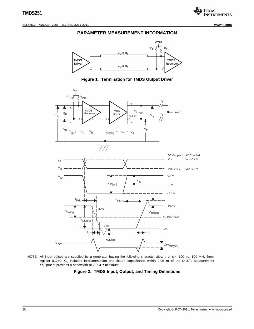
PARAMETER MEASUREMENT INFORMATION
Figure 1. Termination for TMDS Output Driver
NOTE: All input pulses are supplied by a generator having the following characteristics: tr or tf < 100 ps, 100 MHz fromAgilent 81250. CL includes instrumentation and fixture capacitance within 0.06 m of the D.U.T. Measurementequipment provides a bandwidth of 20 GHz minimum.
Figure 2. TMDS Input, Output, and Timing Definitions
10 Copyright © 2007–2011, Texas Instruments Incorporated

TMDSDriver
0 V or 3.6 V
50
50
_+
IOS
50%
VOLtsk(D)
VY
VZ
VOH
Data +
Data -
Clk+
Clk-
Video PattermGenerator
1000 mVpp
Differential
Coax
Coax
Coax
Coax
Coax
Coax
Coax
Coax
<2" 50!
Transmission Line
TMDS251
RX
+EQ
M
UX
OUT
RX
+EQ
M
UX
OUT
<2" 50!
Transmission Line
<2" 50!
Transmission Line
<2" 50!
Transmission Line
SMA
SMA
SMA
SMA
SMA
SMA
SMA
SMA
AVcc
RT RT
AVcc
RT RT
Jitter TestInstrument
Jitter TestInstrument
TP3TP2TP1
HDMI Cables
TMDS251
www.ti.com SLLS852A –AUGUST 2007–REVISED JULY 2011
PARAMETER MEASUREMENT INFORMATION (continued)
Figure 3. Short Circuit Output Current Test Circuit
Figure 4. Definition of Intra-Pair Differential Skew
A. HDMI 1.3 compliant cable when EQ = Low, and 10m 28AWG input cable when EQ = High.
B. All jitters are measured in BER of 10-9
C. The residual jitter reflects the total jitter measured at the output of the DUT, TP3, subtract the total jitter from thesignal generator, TP1
Figure 5. Jitter Test Circuit
Copyright © 2007–2011, Texas Instruments Incorporated 11

S1
Clocking
S2
Port 1
Port 2
tSX
A
B
A
B
Output
tentdis
Hi-Z
75 mV
VDD2
VDD
0V
-75 mV
75 mV
-75 mV
tSX
HPD1
HPD2
S1
0.4 V
2.4 V
SDA_SINK
SDA1
SDA2
S2
VDD2
VDD2
0V
VDD
1.5V
1.5V
VDD2
HPD_SINK
tpd(HPD) tpd(HPD) tsx(HPD)
tsx(DDC)
tpd(DDC)tpd(DDC)
TMDS251
SLLS852A –AUGUST 2007–REVISED JULY 2011 www.ti.com
PARAMETER MEASUREMENT INFORMATION (continued)
Figure 6. TMDS Outputs Control Timing Definitions
Figure 7. Port Switch Timing Definitions
12 Copyright © 2007–2011, Texas Instruments Incorporated
0
50
100
150
200
250 450 650 850 1050 1250 1450 1650 1850 2450
Signal Rate - Mbps
I-
Su
pp
ly C
urr
en
t -
mA
CC
S1 = S2 = HIGH
S1 = HIGH S2 = LOW IDD
V = AV = 3.3 V, T = 25°C,
TP1 V = 1200 mV , R = 4.02 k ,
Am/Bm(2:4) HDMI Data pattern, 250 Mbps-2.5 GbpsAm/Bm(1) Clock, 25 MHz-250 MHz
CC CC A
ID(PP) PP VSADJ W
0
50
100
150
200
0 10 20 30 40 50 60 70T - Free Air Temperature - CA °
I-
Su
pp
ly C
urr
en
t -
mA
CC
S1 = S2 = HIGH
S1 = HIGH S2 = LOW IDD
V = AV = 3.3 V,
V = 1200 mV , R = 4.02 k ,
Am/Bm(2:4) HDMI Data pattern,Am/Bm(1) Clock
CC CC
ID(PP) PP VSADJ W
2.5-Gbps250-MHz
0
1
2
3
4
5
75 95 115 148.5 185 225
f - Frequency - MHz
Peak-t
o-P
eak J
itte
r -
% T
bit
EQ = LOW 3m 30 AWG
EQ = LOW 5m 28 AWG
EQ = HIGH 10m 28 AWG
EQ = HIGH 15m 26 AWG
See Note A
0
5
10
15
20
750 950 1150 1485 1850 2250
Signal Rate - Mbps
Peak-t
o-P
eak J
itte
r -
% T
bit
EQ = HIGH 10m 28 AWG
EQ = LOW 3m 30 AWG
EQ = LOW5m 28 AWG
EQ = HIGH15m 26 AWG
See Note A
TMDS251
www.ti.com SLLS852A –AUGUST 2007–REVISED JULY 2011
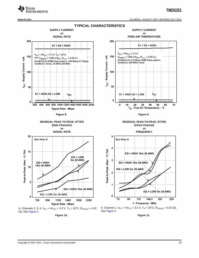
TYPICAL CHARACTERISTICSSUPPLY CURRENT SUPPLY CURRENT
vs vsSIGNAL RATE FREE-AIR TEMPERATURE
Figure 8. Figure 9.
RESIDUAL PEAK-TO-PEAK JITTER RESIDUAL PEAK-TO-PEAK JITTER(Data Channels) (Clock Channel)
vs vsSIGNAL RATE FREQUENCY
A. Channel 1, VCC = AVCC = 3.3 V, TA = 25°C, RVSADJ = 4.02 kΩ,A. Channels 2, 3, 4, VCC = AVCC = 3.3 V, TA = 25°C, RVSADJ = 4.02See Figure 5kΩ, See Figure 5
Figure 10. Figure 11.
Copyright © 2007–2011, Texas Instruments Incorporated 13

0
2
4
6
8
10
12
14
16
18
20
1.5m30AWG
3m 30AWG
5m28AWG
10m28AWG
15m26AWG
EQ = Low
Peak-t
o-P
eak J
itte
r -
% T
bit
Cable
EQ = High
See Note A
0
5
10
15
20
1.5m
30AWG
3m 30
AWG
5m 10m
28AWG
15m
26AWG
EQ = Low
EQ = High
Peak-t
o-P
eak J
itte
r -
% T
bit
28AWG
Cable
See Note A
TMDS251
SLLS852A –AUGUST 2007–REVISED JULY 2011 www.ti.com
TYPICAL CHARACTERISTICS (continued)RESIDUAL PEAK-TO-PEAK JITTER RESIDUAL PEAK-TO-PEAK JITTER
(Data Channel) (Data Channel)vs vs
CABLE CABLE
A. 1080p 10-Bit, VCC = AVCC = 3.3 V, TA = 25°C, RVSADJ = 4.02 kΩ, A. 1080p 12-Bit, VCC = AVCC = 3.3 V, TA = 25°C, RVSADJ = 4.02 kΩ,See Figure 5, Clock Channel = 185.6 MHz, Data Channel = 1.856 See Figure 5, Clock Channel = 222.8 MHz, Data Channel = 2.228Gbps Gbps
Figure 12. Figure 13.
14 Copyright © 2007–2011, Texas Instruments Incorporated

-13
-12
-11
-10
-9
-8
-7
-6
-5
-4
-3
-2
-1
0
0 250 500 750 1000 1250 1500 1750 2000
f - Frequency - MHz
Lo
ss -
dB
spec
EQ = Low
3m 30 AWG cable
TMDS251
www.ti.com SLLS852A –AUGUST 2007–REVISED JULY 2011
APPLICATION INFORMATION
Supply Voltage
The TMDS251 is powered up with two different power sources. One is 3.3-V VCC for the TMDS circuitry, and theother is 5-V VDD for HPD, DDC, and most of the control logic. It is recommended to provide the same 3.3-Vpower source to the TMDS circuitry of the TMDS251 and its output termination voltage. This minimizes theleakage current from the ESD protection circuitry. When the digital television (DTV) is in standby mode operation,the same common 3.3-V power source can be turned on or off. Either way will minimize the leakage current inthe device, and in the receiver connected at the output where the termination is integrated.
TMDS Inputs
Selectable frequency response equalization circuitries are provided to all twelve differential input to support shortrange and long range cable connections. The frequency response compensation curves and target cable lossesare shown in Figure 14 and Figure 15.
Figure 14. Frequency Response Compensation Curve at EQ = L
Copyright © 2007–2011, Texas Instruments Incorporated 15

-20
-18
-16
-14
-12
-10
-8
-6
-4
-2
0
0 250 500 750 1000 1250 1500 1750 2000
f - Frequency - MHz
Lo
ss -
dB
spec
10m cable
EQ = High
VCC
RINTRINT
TMDSReceiver
TMDSDriver
RT
RT
Y
Z
A
B
AVCC
TMDS251
SLLS852A –AUGUST 2007–REVISED JULY 2011 www.ti.com
Figure 15. Frequency Response Compensation Curve at EQ = H
Internal termination circuitry which can be switched on or off, provides 50-Ω resistance to each differential inputpin when a port is selected. External terminations are not required. When the termination is switched on, currentwill flow to the TMDS driver. When a port is not selected, the termination is open. This stops supply currentflowing from the input pins of the unselected ports. This switchable termination provides the connected HDMIsource another method of determining the sink port status, and whether it is selected or not selected, withoutreferring to the HPD pin status.
TMDS Input Fail-Safe
The TMDS input does not incorporate a fail-safe circuit. To implement fail-safe, the input can be externally biasedto prevent output oscillation. One pin can be pulled high to VCC with the other grounded through a 1-kΩ resistoras shown in Figure 16.
Figure 16. TMDS Input Fail-Safe Recommendation
TMDS Outputs
A 10% precision resistor, 4.02-kΩ, is recommended to control the output swing to the HDMI compliant 400 mV to600 mV range (500 mV typical). The TMDS outputs are high impedance under standby mode operation, S1 = Hand S2 = L.
16 Copyright © 2007–2011, Texas Instruments Incorporated

RupSource
VDDSource
Source Sink
RonSCL_SINK
SDA_SINKSCL
SDA
Driver (Source)
I to-Sink
I to-Source
VDDSink
RupSink
VCCRx
RupRx
Driver (Sink)
Ito Sink Vdd Vol(Sink)max
RupSource RupSink
lto Sink Vdd
RupSource RupSink
Vith(Source)min lto Sink Ron Vol(Sink)max
RupSink Vdd Ron RupSource
(Vith(Source)min Vol(Sink)max) RupSource Vdd Ron
RupRx VccRx Ron
(Vith(Sink)min Vol(Source)max)
TMDS251
www.ti.com SLLS852A –AUGUST 2007–REVISED JULY 2011
HPD Pins
The HPD circuits are powered by the 5-V supply. They provide 5-V TTL output signals to the SOURCE with atypical 1-kΩ output resistance. An external 1-kΩ resistor is not needed here. The HPD output of the selectedsource port follows the logic level of the HPD_SINK input. Unselected HPD outputs are kept low. When thedevice is in standby mode, all HPD outputs follow HPD_SINK. A 1-kΩ resistor to ground keeps all HPD outputslow in standby mode if a fixed low state is preferred.
DDC Channels
The DDC circuits (SDA, SCL) are powered by a 5-V supply. The I/O pins can connect to the 5-V terminationvoltages directly. A 47-kΩ pull-up resistor to the 5 V is recommended on the SCL1 and SCL2 pins. There is nopull-up resistor on the SDA pins. The pull-up resistor can be replaced with a different value.
Figure 17. Simplified Electrical Circuit Model for DDC Channel
In Figure 17, when the Driver (Sink) pulls the bus low, the highest voltage level is Vol(Sink)max. The current flowthrough the pass-gate resistor can be presented as:
(1)
where the Vddsource = Vddsink = Vdd
To simplify the equation, Vol(Sink)max is set equal to 0 V to reach equation (2):
(2)
The voltage at the input of the SINK is Ito - Sink × Ron + Vol(Sink)max, which should be lower than the minimuminput low threshold voltage of the Driver (Source), Vith(Source)min to keep the bus in correct interoperations.
(3)
By combining equations (2) and (3), the minimum pull-up resistor at the Sink input is:
(4)
Applying the same methodology to calculate the pull-up resistor at the input of the Driver (Sink), the minimumpull-up resistor is:
(5)
The data sheet VPASS specification ensures the maximum output voltage is clamped at 3.6 V to support a 3.3-Vconnection. Resistors pulling up to 3.3 V on SCL_SINK and SDA_SINK ensure the high level does not exceedthe 3.3-V termination voltage.
Copyright © 2007–2011, Texas Instruments Incorporated 17

TMDS251
SLLS852A –AUGUST 2007–REVISED JULY 2011 www.ti.com
Layout Considerations
The high-speed differential TMDS inputs are the most critical paths for the TMDS251. There are severalconsiderations to minimize discontinuities on these transmission lines between the connectors and the device:• Maintain 100-Ω differential transmission line impedance into and out of the TMDS251• Keep an uninterrupted ground plane beneath the high-speed I/Os• Keep the ground-path vias to the device as close as possible to allow the shortest return current path• Keep the trace lengths of the TMDS signals between connector and device as short as possible
Using the TMDS251 in Systems with Different CEC Link Requirements
The TMDS251 supports a DTV with up to three HDMI inputs when used in conjunction with a signal-port HDMIreceiver or three HDMI inputs when used in conjunction with a dual-port HDMI receiver. Figure 18 and Figure 19show simplified application block diagrams for the TMDS251 in different DTVs with different consumer electroniccontrol (CEC) requirements. The CEC is an optional feature of the HDMI interface for centralizing and simplifyinguser control instructions from multiple audio/video products in an inter-connected system, even when all theaudio/video products are from different manufacturers. This feature minimizes the number of remote controls in asystem, as well as reducing the number of times buttons need to be pressed.
A DTV Supporting a Passive CEC Link
In Figure 18, the DTV does not have the capability of handling CEC signals, but allows CEC signals to pass overthe CEC bus. The source selection is done by the control command of the DTV. The user cannot force thecommand from any audio/video product on the CEC bus. The selected source reads the E-EDID data afterreceiving an asserted HPD signal. The micro-controller loads different CEC physical addresses while changingthe source by means of the S1 and S2 pins.
E-EDID Reading Configurations in Standby Mode
When the DTV system is in standby mode, the sources will not read the E-EDID memory because the 1-kΩpull-down resistor keeping the HPD_SINK input at logic low forces all HPD pins to output logic low to all sources.The source will not read the E-EDID data with a low on HPD signal. However, if reading the E-EDID data in thesystem standby mode is preferred, then TMDS251 can still support this need.
The recommended configuration sequences are:1. Apply the same 3.3-V power to the VCC of TMDS251 and the TMDS line termination at the HDMI receiver2. Turn off VCC, and keep VDD on. The TMDS circuit is off, but the HPD, the DDC and the source selection
circuits are active.3. Set S1 and S2 to select the source port which is allowed to read the E-EDID memory.
Please note if the source has a time-out limitation between the 5 V and the HPD signals, the above configurationis not applicable. Uses individual EEPROMs assigned for each input port, see Figure 19. The solution usesE-EDID data to be readable during system power off or standby mode operations.
18 Copyright © 2007–2011, Texas Instruments Incorporated

SINK
HPD1
SDA1
SCL1
A21/B11
A22/B12
A23/B13A24/B14
HPD2
SDA2
SCL2
A21/B21
A22/B22
A23/B23
A24/B24
EQ
S1
S2
HPD_SINK
SDA_SINK
SCL_SINK
Y1/Z1Y2/Z2
Y3/Z3
Y4/Z4
VSadj
VDD
(5V)
VCC
(3.3V)
GND
E-EDID
HDMI RX
DDC_SDA
DDC_SCL
Y1/Z1Y2/Z2Y3/Z3
Y4/Z4
5V
5V
47kW
47kWmController
3.3V
4.7kW 4.7kW
CEC
CEC
4.02kW 10%
1kW
HPD5V
SDASCL
CEC
CLKD0
D1
D2
HPD5V
SDA
SCL
CEC
CLK
D0
D1
D2
HPD5V
SDA
SCLCEC
CLK
D0
D1D2
SOURCE 1
HPD5V
SDASCL
CEC
CLKD0
D1
D2
SOURCE 2
TMDS251
www.ti.com SLLS852A –AUGUST 2007–REVISED JULY 2011
Figure 18. Two-Port HDMI Enabled DTV with TMDS251 – CEC Commands Passing Through
A DTV Supporting an Active CEC Link
In Figure 19, R, and S, the CEC PHY and CEC LOGIC functions are added. The DTV can initiate and/or react toCEC signals from its remote control or other audio/video products on the same CEC bus. All sources must havetheir own CEC physical address to support the full functionality of the CEC link.
A source reads its CEC physical address stored its E-EDID memory after receiving a logic-high from the HPDfeedback. When HPD is high, the sink-assigned CEC physical address should be maintained. Otherwise, whenHPD is low the source sets CEC physical address value to (F.F.F.F).
Case 1 – AC Coupled Source (See Figure 19, Port 1)
When the source TMDS lines are AC coupled or when the source cannot detect the TMDS termination providedin the connected sink, the indication of the source selection can only come from the HPD signal. The TMDS251HPD1 pin should be applied directly as the HPD signal back to the source.
Case 2 – DC Coupled Source (See Figure 19, Port 2)
When the source TMDS lines are DC coupled, there are two methods to inform the source that it is the activesource to the sink. One is checking the HPD signal from the sink, and the other is checking the terminationcondition in the sink.
In a full CEC operation mode, the HPD signal is set high whether the port is selected or not. The source loadsand maintains the CEC physical address when HPD is high. As soon as HPD goes low, the source loses theCEC physical address. To keep the CEC physical address to the source, the HPD signal is looping back from thesource provided 5-V signal through a 1-kΩ pull-up resistor in the sink. This method is acceptable in applicationwhere the HDMI transmitter can detect the receiver termination by current sensing, and the receiver hasswitchable termination on the TMDS inputs. The internal termination resistors are connected to the terminationvoltage when the port is selected, or they are disconnected when the port is not selected. The TMDS251features switchable termination on the TMDS inputs.
Case 3 – External Logic Control for HPD (See Figure 19, Port 3)
When the HDMI transmitter does not have the capability of detecting the receiver termination, using the HPDsignal as a reference for sensing port selections is the only possible method. External control logic for switchingthe connections of the HPD signals between the HPD pins of the TMDS251 and the 5-V signal from the sourceprovides a good solution.
Copyright © 2007–2011, Texas Instruments Incorporated 19

SINK
HDMI RX
DDC_SDA
DDC_SCL
Y1/Z1
Y2/Z2Y3/Z3
Y4/Z4
5V
47kW
3.3V
4.7kW 4.7kW
CEC
4.02kW 10%
E-EDID
mController
HPDx
SDAx
SCLx
Ax1/Bx1
Ax2/Bx2
Ax3/Bx3
Ax4/Bx4
EQ
S1
S2
HPD_SINK
SDA_SINK
SCL_SINK
Y1/Z1Y2/Z2
Y3/Z3
Y4/Z4
VSadj
VDD
(5V)
VCC
(3.3V)
GND
SDA SCL
CEC
LOGIC
CECPHY
1kW
HPD
5V
SDA
SCL
CEC
CLK
D0
D1
D2
HPD
5V
SDA
SCL
CEC
CLKD0
D1
D2
SOURCEwith AC coupled
HDMI output
SINK
HDMI RX
DDC_SDA
DDC_SCL
Y1/Z1
Y2/Z2Y3/Z3
Y4/Z4
3.3V
4.7kW 4.7kW
4.02kW 10%
mController
HPDx
SDAx
SCLx
Ax1/Bx1
Ax2/Bx2
Ax3/Bx3
Ax4/Bx4
EQ
S1
S2
HPD_SINK
SDA_SINK
SCL_SINK
Y1/Z1Y2/Z2
Y3/Z3
Y4/Z4
VSadj
VDD
(5V)
VCC
(3.3V)
GND
SDA SCL
CEC
LOGIC
1kW
5V47kW
CEC E-EDID
1kWHPD
5V
SDA
SCL
CEC
CLK
D0
D1
D2
HPD
5V
SDA
SCL
CEC
CLK
D0
D1
D2
SOURCEwith DC coupled
HDMI output
CEC
PHY
TMDS251
SLLS852A –AUGUST 2007–REVISED JULY 2011 www.ti.com
E-EDID Reading Configurations in Standby Mode
When the TMDS251 is in standby mode operation, S1 = H and S2 = L, all sources can read their E-EDIDmemories simultaneously with all HPD pins following HPD_SINK in logic-high. HPD_SINK input low will preventE-EDID reading in standby mode operation.
Figure 19. Two-Port HDMI Enabled DTV with TMDS251 – AC Coupled Source - CEC Commands Active
Figure 20. Two-Port HDMI Enabled DTV with TMDS251 – DC Coupled Source - CEC Commands Active
20 Copyright © 2007–2011, Texas Instruments Incorporated

SINK
HDMI RX
DDC_SDA
DDC_SCL
Y1/Z1
Y2/Z2Y3/Z3
Y4/Z4
3.3V
4.7kW 4.7kW
4.02kW 10%
mController
HPDx
SDAx
SCLx
Ax1/Bx1
Ax2/Bx2
Ax3/Bx3
Ax4/Bx4
EQ
S1
S2
HPD_SINK
SDA_SINK
SCL_SINK
Y1/Z1Y2/Z2
Y3/Z3
Y4/Z4
VSadj
VDD
(5V)
VCC
(3.3V)
GND
SDA SCL
CEC
LOGIC
CECPHY
1kW
5V
47kW
CEC E-EDID
1kWHPD
5V
SDA
SCL
CEC
CLK
D0
D1
D2
HPD
5V
SDA
SCL
CEC
CLK
D0
D1
D2
SOURCE
in general HDMI output
TMDS251
www.ti.com SLLS852A –AUGUST 2007–REVISED JULY 2011
Figure 21. Two-Port HDMI Enabled DTV with TMDS251 – External Logic - CEC Commands Active
SpacerREVISION HISTORY
Changes from Original (August 2007) to Revision A Page
• Added Junction Temperature to the THERMAL CHARACTERISTICS table ....................................................................... 7
Copyright © 2007–2011, Texas Instruments Incorporated 21

PACKAGE OPTION ADDENDUM
www.ti.com 10-Jun-2014
Addendum-Page 1
PACKAGING INFORMATION
Orderable Device Status(1)
Package Type PackageDrawing
Pins PackageQty
Eco Plan(2)
Lead/Ball Finish(6)
MSL Peak Temp(3)
Op Temp (°C) Device Marking(4/5)
Samples
TMDS251PAGR ACTIVE TQFP PAG 64 1500 Green (RoHS& no Sb/Br)
CU NIPDAU Level-3-260C-168 HR 0 to 70 TMDS251
(1) The marketing status values are defined as follows:ACTIVE: Product device recommended for new designs.LIFEBUY: TI has announced that the device will be discontinued, and a lifetime-buy period is in effect.NRND: Not recommended for new designs. Device is in production to support existing customers, but TI does not recommend using this part in a new design.PREVIEW: Device has been announced but is not in production. Samples may or may not be available.OBSOLETE: TI has discontinued the production of the device.
(2) Eco Plan - The planned eco-friendly classification: Pb-Free (RoHS), Pb-Free (RoHS Exempt), or Green (RoHS & no Sb/Br) - please check http://www.ti.com/productcontent for the latest availabilityinformation and additional product content details.TBD: The Pb-Free/Green conversion plan has not been defined.Pb-Free (RoHS): TI's terms "Lead-Free" or "Pb-Free" mean semiconductor products that are compatible with the current RoHS requirements for all 6 substances, including the requirement thatlead not exceed 0.1% by weight in homogeneous materials. Where designed to be soldered at high temperatures, TI Pb-Free products are suitable for use in specified lead-free processes.Pb-Free (RoHS Exempt): This component has a RoHS exemption for either 1) lead-based flip-chip solder bumps used between the die and package, or 2) lead-based die adhesive used betweenthe die and leadframe. The component is otherwise considered Pb-Free (RoHS compatible) as defined above.Green (RoHS & no Sb/Br): TI defines "Green" to mean Pb-Free (RoHS compatible), and free of Bromine (Br) and Antimony (Sb) based flame retardants (Br or Sb do not exceed 0.1% by weightin homogeneous material)
(3) MSL, Peak Temp. - The Moisture Sensitivity Level rating according to the JEDEC industry standard classifications, and peak solder temperature.
(4) There may be additional marking, which relates to the logo, the lot trace code information, or the environmental category on the device.
(5) Multiple Device Markings will be inside parentheses. Only one Device Marking contained in parentheses and separated by a "~" will appear on a device. If a line is indented then it is a continuationof the previous line and the two combined represent the entire Device Marking for that device.
(6) Lead/Ball Finish - Orderable Devices may have multiple material finish options. Finish options are separated by a vertical ruled line. Lead/Ball Finish values may wrap to two lines if the finishvalue exceeds the maximum column width.
Important Information and Disclaimer:The information provided on this page represents TI's knowledge and belief as of the date that it is provided. TI bases its knowledge and belief on informationprovided by third parties, and makes no representation or warranty as to the accuracy of such information. Efforts are underway to better integrate information from third parties. TI has taken andcontinues to take reasonable steps to provide representative and accurate information but may not have conducted destructive testing or chemical analysis on incoming materials and chemicals.TI and TI suppliers consider certain information to be proprietary, and thus CAS numbers and other limited information may not be available for release.
In no event shall TI's liability arising out of such information exceed the total purchase price of the TI part(s) at issue in this document sold by TI to Customer on an annual basis.

PACKAGE OPTION ADDENDUM
www.ti.com 10-Jun-2014
Addendum-Page 2

TAPE AND REEL INFORMATION
*All dimensions are nominal
Device PackageType
PackageDrawing
Pins SPQ ReelDiameter
(mm)
ReelWidth
W1 (mm)
A0(mm)
B0(mm)
K0(mm)
P1(mm)
W(mm)
Pin1Quadrant
TMDS251PAGR TQFP PAG 64 1500 330.0 24.4 13.0 13.0 1.5 16.0 24.0 Q2
PACKAGE MATERIALS INFORMATION
www.ti.com 14-Jul-2012
Pack Materials-Page 1

*All dimensions are nominal
Device Package Type Package Drawing Pins SPQ Length (mm) Width (mm) Height (mm)
TMDS251PAGR TQFP PAG 64 1500 367.0 367.0 45.0
PACKAGE MATERIALS INFORMATION
www.ti.com 14-Jul-2012
Pack Materials-Page 2

MECHANICAL DATA
MTQF006A – JANUARY 1995 – REVISED DECEMBER 1996
POST OFFICE BOX 655303 • DALLAS, TEXAS 75265
PAG (S-PQFP-G64) PLASTIC QUAD FLATPACK
0,13 NOM
0,25
0,450,75
Seating Plane
0,05 MIN
4040282/C 11/96
Gage Plane
33
0,170,27
16
48
1
7,50 TYP
49
64
SQ
9,80
1,050,95
11,8012,20
1,20 MAX
10,20SQ
17
32
0,08
0,50 M0,08
0°–7°
NOTES: A. All linear dimensions are in millimeters.B. This drawing is subject to change without notice.C. Falls within JEDEC MS-026


IMPORTANT NOTICE
Texas Instruments Incorporated (TI) reserves the right to make corrections, enhancements, improvements and other changes to itssemiconductor products and services per JESD46, latest issue, and to discontinue any product or service per JESD48, latest issue. Buyersshould obtain the latest relevant information before placing orders and should verify that such information is current and complete.TI’s published terms of sale for semiconductor products (http://www.ti.com/sc/docs/stdterms.htm) apply to the sale of packaged integratedcircuit products that TI has qualified and released to market. Additional terms may apply to the use or sale of other types of TI products andservices.Reproduction of significant portions of TI information in TI data sheets is permissible only if reproduction is without alteration and isaccompanied by all associated warranties, conditions, limitations, and notices. TI is not responsible or liable for such reproduceddocumentation. Information of third parties may be subject to additional restrictions. Resale of TI products or services with statementsdifferent from or beyond the parameters stated by TI for that product or service voids all express and any implied warranties for theassociated TI product or service and is an unfair and deceptive business practice. TI is not responsible or liable for any such statements.Buyers and others who are developing systems that incorporate TI products (collectively, “Designers”) understand and agree that Designersremain responsible for using their independent analysis, evaluation and judgment in designing their applications and that Designers havefull and exclusive responsibility to assure the safety of Designers' applications and compliance of their applications (and of all TI productsused in or for Designers’ applications) with all applicable regulations, laws and other applicable requirements. Designer represents that, withrespect to their applications, Designer has all the necessary expertise to create and implement safeguards that (1) anticipate dangerousconsequences of failures, (2) monitor failures and their consequences, and (3) lessen the likelihood of failures that might cause harm andtake appropriate actions. Designer agrees that prior to using or distributing any applications that include TI products, Designer willthoroughly test such applications and the functionality of such TI products as used in such applications.TI’s provision of technical, application or other design advice, quality characterization, reliability data or other services or information,including, but not limited to, reference designs and materials relating to evaluation modules, (collectively, “TI Resources”) are intended toassist designers who are developing applications that incorporate TI products; by downloading, accessing or using TI Resources in anyway, Designer (individually or, if Designer is acting on behalf of a company, Designer’s company) agrees to use any particular TI Resourcesolely for this purpose and subject to the terms of this Notice.TI’s provision of TI Resources does not expand or otherwise alter TI’s applicable published warranties or warranty disclaimers for TIproducts, and no additional obligations or liabilities arise from TI providing such TI Resources. TI reserves the right to make corrections,enhancements, improvements and other changes to its TI Resources. TI has not conducted any testing other than that specificallydescribed in the published documentation for a particular TI Resource.Designer is authorized to use, copy and modify any individual TI Resource only in connection with the development of applications thatinclude the TI product(s) identified in such TI Resource. NO OTHER LICENSE, EXPRESS OR IMPLIED, BY ESTOPPEL OR OTHERWISETO ANY OTHER TI INTELLECTUAL PROPERTY RIGHT, AND NO LICENSE TO ANY TECHNOLOGY OR INTELLECTUAL PROPERTYRIGHT OF TI OR ANY THIRD PARTY IS GRANTED HEREIN, including but not limited to any patent right, copyright, mask work right, orother intellectual property right relating to any combination, machine, or process in which TI products or services are used. Informationregarding or referencing third-party products or services does not constitute a license to use such products or services, or a warranty orendorsement thereof. Use of TI Resources may require a license from a third party under the patents or other intellectual property of thethird party, or a license from TI under the patents or other intellectual property of TI.TI RESOURCES ARE PROVIDED “AS IS” AND WITH ALL FAULTS. TI DISCLAIMS ALL OTHER WARRANTIES ORREPRESENTATIONS, EXPRESS OR IMPLIED, REGARDING RESOURCES OR USE THEREOF, INCLUDING BUT NOT LIMITED TOACCURACY OR COMPLETENESS, TITLE, ANY EPIDEMIC FAILURE WARRANTY AND ANY IMPLIED WARRANTIES OFMERCHANTABILITY, FITNESS FOR A PARTICULAR PURPOSE, AND NON-INFRINGEMENT OF ANY THIRD PARTY INTELLECTUALPROPERTY RIGHTS. TI SHALL NOT BE LIABLE FOR AND SHALL NOT DEFEND OR INDEMNIFY DESIGNER AGAINST ANY CLAIM,INCLUDING BUT NOT LIMITED TO ANY INFRINGEMENT CLAIM THAT RELATES TO OR IS BASED ON ANY COMBINATION OFPRODUCTS EVEN IF DESCRIBED IN TI RESOURCES OR OTHERWISE. IN NO EVENT SHALL TI BE LIABLE FOR ANY ACTUAL,DIRECT, SPECIAL, COLLATERAL, INDIRECT, PUNITIVE, INCIDENTAL, CONSEQUENTIAL OR EXEMPLARY DAMAGES INCONNECTION WITH OR ARISING OUT OF TI RESOURCES OR USE THEREOF, AND REGARDLESS OF WHETHER TI HAS BEENADVISED OF THE POSSIBILITY OF SUCH DAMAGES.Unless TI has explicitly designated an individual product as meeting the requirements of a particular industry standard (e.g., ISO/TS 16949and ISO 26262), TI is not responsible for any failure to meet such industry standard requirements.Where TI specifically promotes products as facilitating functional safety or as compliant with industry functional safety standards, suchproducts are intended to help enable customers to design and create their own applications that meet applicable functional safety standardsand requirements. Using products in an application does not by itself establish any safety features in the application. Designers mustensure compliance with safety-related requirements and standards applicable to their applications. Designer may not use any TI products inlife-critical medical equipment unless authorized officers of the parties have executed a special contract specifically governing such use.Life-critical medical equipment is medical equipment where failure of such equipment would cause serious bodily injury or death (e.g., lifesupport, pacemakers, defibrillators, heart pumps, neurostimulators, and implantables). Such equipment includes, without limitation, allmedical devices identified by the U.S. Food and Drug Administration as Class III devices and equivalent classifications outside the U.S.TI may expressly designate certain products as completing a particular qualification (e.g., Q100, Military Grade, or Enhanced Product).Designers agree that it has the necessary expertise to select the product with the appropriate qualification designation for their applicationsand that proper product selection is at Designers’ own risk. Designers are solely responsible for compliance with all legal and regulatoryrequirements in connection with such selection.Designer will fully indemnify TI and its representatives against any damages, costs, losses, and/or liabilities arising out of Designer’s non-compliance with the terms and provisions of this Notice.
Mailing Address: Texas Instruments, Post Office Box 655303, Dallas, Texas 75265Copyright © 2017, Texas Instruments Incorporated