Embed Size (px)
Citation preview

Revie o
June 1980 Volume 41 No. 2
RCARCI 41 (2) 131-270 (1980)

RCA Review, published quarterly in March, June, September and De- cember by RCA Research and Engi- neering, RCA Corporation, Princeton, New Jersey 08540. Entered as second class matter July 3, 1950 under the Act of March 3, 1879. Second-class postage paid at Princeton, New Jer- sey, and at additional mailing offices. Effective January 1, 1978, subscrip- tion rates as follows: United States and Canada: one year $8.00, two years $ 14.00, three years $18.00; in other countries, one year $8.60, two years $15.20, three years $19.80. Single copies (except for special issues) up to five years old $3.00.
The cover figure represents the front side of a single -crystal silicon solar cell. The white pattern is the metalli- zation grid and the bonding area used for electrical lead attachment. The cell was coated with an antireflective film of TiO2 by the spray -on process de- scribed in the Kern/Tracy paper in this issue. The antireflection coating, which exhibits a deep blue interfer- ence color on silicon, is only one quarter -wavelength thick but effects an increase in the photovoltaic con- version efficiency of the cell by over 40 percent.

nucea Review
Contents
RCA Review (ISSN 0033-6331) is a techrical journal published quarterly by RCA Research and
Engineering in cooperation with the subsidiaries and divisions of RCA.
133 Titanium Dioxide Antireflection Coating for Silicon Solar Cells by Spray Deposi- tion Werner Kern and Edwin Tracy
181 The Measurement of Deep Centers in Float Zone Silicon by Phctovoltege Spec- troscopy L. L. Jastrzebski and J. Lagowski
198 GaAs MESFET Comparators for Gigabit -Rate Analog -to -Digital Converters L. C. Upadhyayula
213 Comparison of Phase -Only and Conventional Monopulse in Thermal Noise Carmen N. Campoplano and Raymond S. Berkowitz
227 Ion Implantation of Sulfur and Silicon in GaAs S. G. Liu, E. C. Douglas, C. P. Wu, C. W. Magee, S. Y. Narayan, S. T. Jolly, F. Kolondra, and S. Jain
263 Patents
265 Authors

RCA Corporation E. H. Griffiths President and Chief Executive Officer
Editorial Advisory Board Chairman, J. J. Tletlen RCA Laboratories
G. C. Hennessy RCA Laboratories E. O. Johnson RCA Research Laboratories. Inc.
H. Kressel RCA Laboratories W. Merz Laboratories RCA, Ltd. K. H. Powers RCA Laboratories L. A. Shotlift International Licensing T. O. Stanley, RCA Laboratories W. M. Webster RCA Laboratories
Editor Ralph F. Ciaf one
Associate Editors D. R. Higgs Missile and Surface Radar Division C. Hoyt Consumer Electronics T. King RCA Research and Engineering R. Mausler National Broadcasting Company M. Rosenthal RCA Americom, Inc. J. Schoen Solid -State Division M. G. Pietz Government and Commercial Systems W. S. Sepich Commercial Communicatons Systems Division J. E. Steoger RCA Service Company D. Tannenbaum Government Communications Systems
© RCA Corporation 1980. All rights reserved, except that express permission is hereby granted for the use in computer -based and other information -service systems of titles and abstracts of papers published in RCA Review.

Titanium Dioxide Antireflection Coating for Silicon Solar Cells by Spray Deposition *
Werner Kern and Edwin Tracy"
RCA Laboratories, Princeton, NJ 08540
Abstract-A high-speed production process is described for depositing a single -layer,
quarter -wavelength thick antireflection coating of titanium dioxide on metal -pat-
terned single -crystal silicon solar cells for terrestial applications. Controlled at-
omization spraying of an organotitanium solution was selected as the most cost effective method of film deposition using commercial automated equipment. The
optimal composition consists of titanium isopropoxide as the titanium source,
n -butyl acetate as the diluent solvent, sec-butanol as the leveling agent, and 2-
ethyl-1-hexanol to render the material uniformly depositable. Application of the
process to the coating of circular, large -diameter solar cells with either screen -
printed silver metallization or with vacuum evaporated Ti/Pd/Ag metallization
showed increases of over 40 percent in the electrical conversion efficiency. Optical characteristics, corrosion resistance, and several other important prop-
erties of the spray -deposited film are reported. Experimental evidence is presented
that indicates a wide tolerance in the coating thickness upon the overall efficiency of the cell. In addition, considerations pertaining to the optimization of AR coatings
in general are discussed and a comprehensive critical survey of the literature is
presented.
1. Introduction
1.1 Overview of Paper
The objective of the work described was the development of a low-cost, mass production process for producing an antiretlection (AR) coating
This work was performed as part of the Low -Cost Solar Array project, Jet Propulsion Laboratory. California Institute of Technology under Contract 954868, and was jointly sponsored by the U.S. De- partment of Energy through an agreement with NASA.
Present address: SERI Branch 641, Golden, Colorado 80401.
RCA Review Vol. 41 June 1980 133

on silicon photovoltaic cells. The process was to be applicable to cells featuring saw -cut and chemically etched (non -planar) surfaces of sin- gle -crystal silicon with metallization grids of screen -printed and fired conductive inks.
Several processes were explored and tested for technical feasibility and cost viability. These processes included physical vapor deposition techniques, such as vacuum evaporation and sputtering processes; chemical vapor deposition at normal and reduced pressure, including plasma -enhanced deposition; and mechanical deposition techniques, such as spinning, dipping/draining, and spraying, followed by chemical conversion of the deposit to a solid AR film.
Several materials of high refractive index were tested for their suit- ability with respect to optical properties, cost effectiveness, and stability. Materials considered included dielectrics such as Ti02, Ti02-Si02, SiO, Ta205, Zr02, Hf02, Si3N4 and SiXNyH as well as electrically conductive and transparent semiconductors such as Sn02, In203, In203:Sn, and Sn02:Sb.
Our final analysis indicated that spray -deposition of organo-metallic titanium compounds followed by chemical reaction to produce films of
SAWCUT SILICON WAFERS
}
ETCH AND RINSE
}
FORM PN-JUNCTION
}
INSPECT AND CLEAN
FURNACE ANNEAL
t SCREEN -PRINT SILVER ON BACK
t SCREEN -PRINT FRONT SILVER GRID
}
FURNACE- SINTER
SPRAY DEPOSIT AR COATING
}
HEAT TREAT AR COATING
}
TEST CELLS ELECTRICALLY
7
INTERCONNECT METALLIZATION
}
LAMINATE DOUBLE GLASS PVB
TEST
Fig. 1-Major steps in the manufacturing sequence of single -crystal silicon solar cells in- dicating the application of the spray -on AR coating.
134 RCA Review Vol. 41 June 1980

ANTIREFLECTION COATING
titanium dioxide met the stated requirements most effectively. Conse- quently, we developed a process on this basis, with the successful result reported in this paper.
In addition, a very comprehensive review of the literature on AR coatings for solar cells is presented which covers references to early 1980)-54 Also, fundamental optical considerations are discussed, since they form the basis of our observations for optimizing the properties of AR films.
Our work on AR coatings has been part of a larger, partly govern- ment -sponsored RCA solar cell development project designed to devise manufacturing sequences that should ultimately he suitable for the mass production of single -crystal silicon photovoltaic array modules at a cost of less than $700 per peak kW (in 1980 dollars). The major steps in the manufacturing sequence investigated at RCA are presented in the flow chart in Fig. 1; it shows at which step in the sequence the AR coating is applied.
1.2 Historical Perspective and Literature Review
Lord Rayleigh is generally credited with the first experimental obser- vation of the antireflection effect in 1887, while Bauer offered the first successful theoretical treatment based on interference effects in 1934." Since then the theory and application of optical interference phem)mena has been well documented, especially with respect to thin film filters, and has resulted in a multi -million dollar optical coating industry. An- tireflection coatings for solar cells, however, are a relatively recent event beginning primarily in the 1960's with the advent of photovoltaics as remote power sources for spacecrafts and satellites.
A comprehensive search of the literature from 1968 to the present was made in an effort to review the types of antireflection coatings used, the deposition methods employed, and the various solar cell substrates upon which they were deposted. Table 1 lists the articles we found to be the most informative; they were carefully reviewed and selected from the initial search and rated with respect to the extent of the author's dis- cussion of antireflection characteristics of the coating (E for extensive, M for moderate, and L for limited in scope). The references themselves are given at the end of the paper. The table shows the AR coating ma- terial, deposition method, and substrate, respectively, in terms of the author's original description. In the few cases where the deposition method was not specified, the abbreviation n.s. indicates the omis- sion.
None of the articles reviewed that were published prior to 1971 were deemed appropriate to include in the table. A quarter -wavelength
RCA Review Vol. 41 June 1980 135

Table 1-Survey Abstract of Literature References Pertaining to AR Coatings
Ref. (Scope of Discussion of AR Coatings)/fear (E = extensive, M = moderate,
L = limited) AR Coating I)eposition Method
(n.s. = not specified) Solar Cell Subst rate
1 (M)/1979
2 (F:1/1979
:3(1.)/1979
4(L)/1979
a9 (M)/1979
50 (E)/1979
5 (1.)/I978
6 (M)/1978
- (L)/1978
8 (L)/1978
9 (L)/1978
51 (1.)/1978
10 (L)/1978
11 (L)/1978
12 (L)/1978
13 (M)/1978
la (L)/1978
15 (M)/1978
16 (M)/1977
17 (M1/1977
18 (M)/1977
Indium tin oxide (ITO)
TiO2
SnO2
SiO
SnO2
ZnS, cryolite
SiO
Ti02, In203
SnO2
'1'a2O5, Nh2O5
TiO2
SiO2-'Ta2O5
Oxide of n+GaAs
SiO. 'TiOx, 'TaxOy, 'ha2O5
All types (review article)
TiO2
Krylon, SiO TiÓx
SiO
TiO, SiO2 Si3N4, SiO2 dual
layer ZnS
Neutralized ion (ream sputtering
Spin -on or dipping with air and vacuum baking at -325°C
300°C -400°C pyroly- sis of SnCl4-H.O- ethyl acetate solu- tions
Evaporat ion
Hydrolysis of SnCI.1
n.s.
n.s.
n.s.
400°C oxidation of tetramethvltin
n.s.
80 100°C hydrolysis of tet raiospropyl titanate
rf diode sputtering of SiO2-'l'a2O5 Targets
Electrolytic anodization
n.s.
n.s.
1110 400°C hydrolysis of tetraisopropyl titanate
n.s. 80-100°C hydrolysis
of tetraisopropyl titanate
Evaporation
Spin -on CV'I) and thermal n.s.
Evaporation
Single crystal silicon ISIS type)
Silicon (round wafer and (tendritic-web ribbon type)
Single -silicon and polvsilicon SnO2/n- Si
n+p single crystal silicon (MIS type)
n+/p single crystal silicon
Ag/p-Si (Schottky barrier type)
Cr/oxide/p-silicon (MIS type)
Single and polycrystalline silicon
Thin film polycrystalline silicon
GaAs (polycrystalline AMOS type)
Thin film GaAs (MOS type)
Fused Silica (for integrated optical circuits)
Shallow-homojunc- tion n4-/p/p+ single crystal GaAs
Silicon (non -reflective, violet type cell)
All types
Silicon, GaAs
Polycrystalline GaAs on tungsten/ graphite substrates
Single crystal and polycrystalline In PI Cds
Silicon (NIIS inversion layer type)
Epi-silicon (concentrator type)
Al/p-type silicon (MIS type)
136 RCA Review Vol. 41 June 1980

ANTIREFLECTION COATING
Table /-(Contd) Ref. (Scope of
Discussion of AR Coat ings)/Year (E = extensive, M = moderate,
L = limited) AR Coating Deposit ion Method (n.s. = not specified) Solar Cell Substrate
19 (L)/1977 TiO2-Sí02 dual layer
n.s. pan+ silicon (concentrator type)
52 (L)/1977 TiO2-SiO2 Spin -on p+/n silicon 20 (M)/1977 Sh903 E -beam and laser
beam evaporation Silicon (AMOS type)
21 (E)/1977 SiO2, Ti0, Ta2O5 n.s. All types 22 (1.)/1977 Glycerol n.s. Cds/CdTe
heterojunction 23 (L)/I977 SnO2 E -beam evaporation SnO2/Si
heterojunction 24 (MI/1977 In2O3 Vacuum evaportion Silicon (MIS type) 25 (M1/1977 SiO, I'i0 Ta205,
CeO2 n.s. Silicon
26 (1)/1977 MgF2 n.s. n-ITO/p-ITO 27 (L)/1977 7.r02, Si3N4 n.s. a -silicon (Schottky
harrier type4 28 (M)/1976 TiO2 Spin -on of tetrahutyl
titanate Silicon
29 (M)/1976 Arsenic -doped SiO2
Spin -on Diffused n+ -p+ silicon
30 (L)/1976 Silicon nitride n.s. Textured silicon 31 (1.)/1976 SiO Evaporation Cr/p-silicon (MIS
type) 32 (E)/1976 Ta2O5 Evaporation Any metal/
semiconductor or Schot t ky barrier t } pe
33 (E)/1976 Ta2O5, N h205 E -beam evaporation Silicon (violet or Comsat non - reflective types)
34 (E)/1976 Ta2O5 Thermal oxidation of metallic Ta
Silicon
35 (MI/1975 SiO, TiOx, Ta205, Nh2O5
n.s. Silicon
36 (M)/1975 Ta2O5, Nh2O5 n.s. Silicon (conventional, violet, and non- retlective type)
37 (M)/1975 Ta2O5 E -Gun evaporation GaAs, GaAs/P (Schottky barrier type)
38 (M)/I975 TiO2-SiO2 Spin -on Silicon (single crystal, p/n diffused
SiO n.s. junction) 39 (L)/1975 Ta2O5, SiO n.s. Silicon (violet and non -
reflective types) 53 (M)/í975 Ta2O5 n.s. Silicon (non -reflective
type) 40 (M)/1975 Ta2O5. SiO n.s. Silicon (shallow
junction type) 41 (L)/1975 SIPOS I1.S. Multilayer epi On
silicon
42 (E)/1975 Ta2O5 E -beam evaporation Au/GaAs (AMOS type)
43 (E)/1974 Ta2O5, N6205. n.s. Silicon (violet type) SiO>, TiO%
RCA Review Vol. 41 June 1980 137

Table l-(Contd) Ref. (Scope of
Discussion of AR Coat ings)/Year (E = extensive, M = moderate,
L = limited)
44 (E)/1974
45 (L)/1974
46 (M)/1973
47 (M)/1972
48 (L)/1972 54 (L)/1972
AR Coating
SiO, S13N4, Ta205 (single and dual layers)
SiO
Ti02, SiO
Si02 Ce02 TiO
SiO,,, TiO Ge
Si
Deposition Method (n.s. = not specified)
n.s.
Vacuum deposition
Vacuum deposition
Thermally grown E -beam evaporation Reactive evaporation
in an 02 atmos- phere
K -beam evaporation CVD of GeH4 3u0 -
450°C CVD of SiH4 325-
575°C
Solar Cell Substrate
Silicon
Silicon (Schottky barrier type)
Cr-silicon (Schottky harrier type)
n/p-si I icon
Silicon Silicon (no cells)
Germanium (no cells)
thickness of SiO (n - 1.8) was practically the only AR coating used on solar cells prior to 197025,35 due to an oversimplification in matching the refractive index of silicon to that of air. Until 1972, investigators in the field were still primarily concerned with improving the characteristics of the cell itself and probably considered AR coatings a peripheral subject. Furthermore, the improvement in .J afforded by SiO was ap- parently considered satisfactory at that stage of development.
Some time later, the realization that cells needed to he encapsulated with an organic adhesive and cover glass prompted research workers to examine the utilization of higher refractive index coatings (n - 2.0) such as TiOx, Si3N4, and CeO2. Subsequently, with the arrival of solar cells having improved short -wavelength response (violet cells), high -index coatings with good transmission extending to A = 0.35 pm for AM = 0 applications were investigated such as Ta205 and Nh205.
The current mode of research emphasis is basically two -fold: (1) low-cost AR coatings capable of high-speed automation for large-scale terrestial applications (AM = 1,2), and (2) transparent conductive coatings, such as In203i Sn02, or In203:Sn, for reducing or eliminating the inactive cell area masked by the opaque top -contact metalliza- tion.
The survey table should prove useful to those interested in quickly acquiring information about a specific AR coating material or about a coating used on a specific type of cell. In addition to the more commonly accepted types of AR coatings, such as SiO, TiO,, Si3N4, Ta205, Sn02, etc., Table 1 lists some rather atypical coating trials with films such as acrylics, glycerol, and SIPOS. A considerable effort has been expended
138 RCA Review Vol. 41 June 1980

ANTIREFLECTION COATING
to include all pertinent papers in this survey to the best of our awareness
and judgment.
1.3 Basic Optical Considerations
The percentage of incident energy reflected from a given substrate de-
pends on the relative indices of refraction across the interface and the angle at which the radiation strikes the surface. With normal incidence, the reflectance (R) from the silicon substrate is given by the Fresnel relation:
R = 1(n1 - n2)/(n 1 + n2)]2, Il l
where n 1 = refractive index of silicon and n2 = refractive index of the surrounding media. For an air interface (n2 = a considerable amount of energy is wasted in reflection from a silicon surface due to its high index of refraction (n.,.; = 3.9 for radiation of ,\ = 0.6 pm).1i1 Substitution of these refractive index values into Eq. ¡11 results in a reflectance loss
of 35%. Without the application of an AR coating, only 65% of the available sunlight is coupled into the cell. Thus, a 100% effective AR coating resulting in zero reflectance and zero absorbance has the theo- retical capability of increasing the electrical output of a silicon solar cell by 54%.
Quarter -wave antireflection (QWAR) coatings of appropriate re-
fractive index and thickness reduce reflection from the silicon surface by reflecting light from the film's front and back surfaces such that the light waves are of equal amplitude and are 180° out of phase, resulting in destructive interference. To satisfy the laws of energy conservation, this light must necessarily be transmitted into the cell rather than being reflected. The optimum index of refraction (na,) of a thin film to achieve
this effect is governed by the following relation:
na, _ /n1 n2. 121
Appropriate substitution results in nar -' 2.0 and ne, 2.4 for silicon cells
in air (n2 = 1) and under a plastic -laminated glass cover (n2 = 1.5), re-
spectively. The film thickness (T1) to achieve minimum reflectance with a QWAR
coating is given by
T -1 X. [31
4 nar
where Xa,;n is the wavelength of light at which a minimum is desired. For
silicon solar cells Xa,;a is usually chosen equal to or very near 0.6 µm, re -
RCA Review Vol. 41 June 1980 139

suiting in an optimum thickness of T1' 750 for an AR coating with a refractive index of 2.2.
Eqs. [1], [2], [3], and related mathematical examples represent an over -simplification of the parameters that must be analyzed to determine the refractive index and thickness of a QWAR coating and are applicable for only one particular wavelength and temperature. Furt her discussion of these parameters with respect to broad -hand antireflection across the solar spectrum and ramifications with respect to spray -on TiO2 coatings will be postponed to a later section of this paper in order to preserve continuity of presentation. (See Sec. 3.5.)
2. Experimental
2.1 Materials
Several organotitanium compounds, numerous types of organic solvents, a few organic surfactant additives, and several acid catalysts were used during the investigation for formulating suitable spray mixtures. The best spray mixture, "RCA-Ti02", is specified in Table 2; it is based on titanium(IV) isopropoxide and was used for processing most of the cells and samples described in this paper. Three other titanium sources were comparatively evaluated using analogous mixture formulations: titan- ium(IV) ethoxide, titanium(IV) butoxide, and "Titaniumsilicafilm C"
Ta Me 2-Components Used to Prepare the Optimized Final Titanium Spray Liquid INCA-TiO2
Composit ion Function Compound Specifications (vol) (vol %) Source
"Titanium titan urn (I \7) source isopropoxide.
TiIOCHI('H;11214 Diluent n-butylacetate.
solvent CH3CO2(CH2)3CH3
Sprayabilit y agent
Leveling agent
2 -et hvl- I -hexanol, CHa(CH213CH- (C2H5)CH2OH
sec-butanol. C2H5CH (OH ICH3 or isopropanol. (CH312CHOH
mp 20°C. cl
0.9550 g/cm3
99+%. by 127°C, d 0.882 g/cnrt
99+%, hp 180 182°C. ci
0.832-0.83:3 g/cm3
99%, hp 98°C. d 50 12 Aldrich 0.808 g/cm3 Chemical
Co. Aldrich
Chemical Co.
99+% anhy- drous. hp 82- 83°C. d 0.785 g/cm3
9.2 7.7 Alfa Division, Vent ron Corp.
20 17 Aldrich Chemical ('o.
40 33 Eastman Organic Chemicals
Spray liquid Composite mixture 1(9.2 100 (prepared from the above ingredients)
140 RCA Review Vol. 41 June 1980

ANTIREFLECTION COATING
spin -on solution concentrate of proprietary composition (Emulsitone Company, Whippany, NJ).
The mixture is prepared by diluting the titanium source liquid with the n -butyl acetate. The 2-ethyl-1-hexanol mixed with the sec-butanol is then added with agitation. The mixture, if stored in the dark in a tightly sealed and full bottle, has a shelf life of at least several months.
Substrate materials consisted of single -crystal, 7.5 -cm diameter silicon solar cells made primarily with POCI;t-diffused junction, and metal patterned by screen -printed silver ink followed by firing resulting in a
film thickness of typically 8µm. Cells with vacuum -evaporated Ti/Pd/Ag metallization of about 2.7 pm film thickness were also used, mainly for comparison. Test substrates consisted of 7.5 -cm diameter single -crystal silicon wafers polished on one side. Plates of fused quartz and microscope glass slides were used for optical transmission measurements.
Chemicals for cleaning test substrates included a hot mixture (1:1 by
volume) of H202 30% - H0SO.t 98%, and of H2O - HF 49% (1:1 by vol-
ume) for stripping oxide layers from silicon wafers. Solar cells usually required no cleaning prior to spray coating. They
were handled and stored to be as free from contamination as possible. Cells that did require cleaning were rinsed in methylethylketone followed by n -butyl acetate and spin-drying.
2.2 Spray Deposition and Heating Equipment
Several types and commercial makes of spray machines were examined for suitability for our purpose. The spray machine (Fig. 2) we used in our laboratory for the pilot production tests was a Series 9000 Autocoater from Zicon Corporation, Mount Vernon, NY. This unit for hatch oper- ation is a smaller and less automated version of the fully automated in -
line Series 11(X)0 machine we consider suitable for large-scale continuous mass production. The spraying is conducted in a closed, class 100, lam- inar downdraft clean -booth supplied with HEPA-filtered air which is
conditioned to a relative humidity not exceeding 45%. The exhaust air exits through a flow -adjustable duct. The spray liquid is contained in
a nitrogen -pressurized stainless steel tank, as seen in Fig. 2, and is
transported through stainless steel tubing to the liquid reservoir above the spray nozzle. The reciprocating spray gun (Figs. 3 and 4) traverses prependicularly to the substrate cells, which are moved by an incre- mental advancing transport mechanism. The machine operates auto- matically over a wide range of programmed cycles adjustable by front - panel controls. A solvent -resistant final filter (0.5 -pm Millipore Filter,
RCA Review Vol. 41 June 1980 141

tí-:; i (,)
Fig. 2-Zicon Series 9000 Autocoater.
l
Fig. 3-Spray gun assembly.
.
142 RCA Review Vol. 41 June 1980

ANTIREFLECTION COATING
©t
tt
Fig. 4-Close-up of atomization spray gun.
Millipore Corporation) has been placed at the exit port of the spray so-
lution reservoir above the spray head to remove any traces of particu- lates. The diameter of the spray nozzle used in our work was 0.33 mm
(0.013 in.). It is important that the air in the spray booth he dust -free and of low
humidity (_45% RH). High humidity can cause premature reaction of the atomized droplets in the gas phase, leading to hazy film deposits.
A perforated metal tray, elevated 1.5 cm above the stainless steel substrate platform, for holding the cells has normally been used to simulate the support mechanism featured in the in -line spray coating machine for continuous mass production. No problems with backside contamination by the spray occurred. in contrast to techniques based on dipping and draining. Our machine accepts comfortably up tc 15 cells
of 7.5 cm diameter. A series of cells being spray coated is shown in Fig.
5. A vapor -exhaust convection oven with thermostatic temperature
control is used for the initial drying of a hatch of coated cells. We have
used a gravity convection oven, but recommend a forced air convection type for improved performance. The subsequent heat treatments at higher temperature of large hatches of cells are carried out in convection ovens in which the cells can he positioned vertically in trays or cassettes for greatly increased packing density. For laboratory processing we have
RCA Review Vol. 41 June 1980 143

IiUp I IIIIItlnhl . gm
111111111111111111
niamiÍit, Ant 'I"lllulllUilllu wing - n"
Fig. 5-Solar cells being spray -coated: front row coated, rear row uncoated.
used Corning PC -100 Pyroceram hotplates covered with an aluminum plate for uniform heat distribution.
A layout plan for large-scale, automated, continuous in -line production spraying and heat treatments is shown in Fig. 6. The cells are transfered
PRODUCT SPRAY
UNIT
AUTOMATIC
CASSETTE
UNLOAD
AIR
FLASH IR PRE -DRY UNIT
AUTOMATIC
CASSETTE
LOAD
200°C! 450°C
OVEN FLOW
PRODUCT
FLOW
AUTOMATIC
CASSETTE UNLOAD
SPRAY
UNIT
AIR
FLASH IR PRE- DRY UNIT
AUTOMATIC
CASSETTE LOAD
200°C/ 450°C
OVEN
Fig. 6-Layout plan for large-scale production equipment. This equipment would occupy an area 20 X 40 feet.
144 RCA Review Vol. 41 June 1980

ANTIREFLECTION COATING
in and out of the conveyor system by automatic cassette unloaders and
reloaders. The estimated production throughput is 4500 cells per hour
per machine. The combined output would correspond to 55 million cells
annual production, assuming continuous operation and 90% machine
uptime. On the basis of 0.54.3 W/cell and a 99% yield this quantity rep-
resents a total of 30 megawatts per year.
2.3 Film Deposition and Heating Treatments
The step at which the AR coating is applied has been shown in the
manufacturing sequence flow chart in Fig. 1. The procedure for spray
coating cells for laboratory production is described below.
The cells as received from metallization sintering are placed on the
perforated substrate tray. The glass doors of the spray booth are closed
and the room air displaced with dry, filtered air. The automatic spray
cycle is activated 10 seconds later. Spray coating of one load of cells takes
half a minute. After the substrate table has returned to its starting po-
sition the doors are opened and the substrate tray is transferred into the
convect ion oven. The automatic spray cycle of the machine can be adjusted according
to the specific requirements of film thickness and throughput. Of the
various variable factors, the source delivery pressure is the major variable
utilized for adjusting the amount of solution sprayed, thereby controlling the resulting solid film thickness. We have typically used a liquid delivery
pressure of 6.97 kPa (28 in. H20). The atomization spray pressure and
the spray gun -to -substrate distance can he used as secondary variables,
but were kept constant at 207 kPa (30 psig) and 17.8 cm with all other
parameters maintained at a specific setting. The first heat treatment immediately after the spray deposition of
the liquid film is performed in a convection oven set to an air temperature
of 95°C. A 40 -sec heating period in the oven has been found equivalent to a previously used 30 -sec heating on a hot plate at 70°C, as determined
by comparing refractive index and thickness changes for the two tech-
niques. 'The humidity level in the first solvent evaporation and film
drying oven should also be low to assure the formation of clear films.
Several trays filled with a thick bed of anhydrous calcium sulfate des-
iccant (Drierite, The W. A. Hammond Drierite Company) remain per-
manently loaded in the oven. The solid but soft and still solvent -soluble film is next treated at 200°C
in room air. We found, by measurements of thickness, refractive index,
and solubility, that substantial property changes have occured by the
end of this treatment. Ambient moisture and oxygen might aid in the
reaction to transform the organometallic to essentially titanium dioxide.
RCA Review Vol. 41 June 1980 145

However, there is no need for controlling the ambient atmosphere other than keeping it clean.
The third and final heat treatment is designed to remove the last traces of organic solvents, to complete the hydrolytic reaction to TiO2, and to densify the film to obtain a stable structure of maximum refractive index. A temperature of 450°C in room air or oxygen is needed to accomplish these objectives. For practical purposes a period of 30 seconds is suffi- cient for each of the heat treatments (200°C and 450°C) if done on hot plates in air. Processing hatch -wise in an oven or continuously in a tube or tunnel furnace is, of course, much more economical even though it requires a longer period of time to achieve thermal equilibrat ion.
2.4 Metallization Bondability After AR Coating
The surface of the metallization grid collector pad must he free of AR coating in order to permit effective bonding of cell -to -cell interconnects. The simplest technique, suitable for laboratory applications, is masking of the pad with a special solvent -resistive polyethylene pressure tape with acrylic adhesive prior to spraying (Tape No. 480, 3M Company, St. Paul, Minn.). The tape tab is readily peeled off after coating but before heat treatments, leaving a clean and bondable surface.
Mechanical and chemical techniques can be used for automated high-speed processing. Selective mechanical removal of the AR coating can he accomplished most readily by momentary application of an au- tomatic ultrasonic vibrating or buffing tool combined with vacuum suction to remove the debris. Alternatively, since the solder connection techniques used require fluxing of the bonding area, a flux composition can be applied that contains a fluoride capable of selectively dissolving the thin AR coating. Rinsing with a jet of deionized water prevents metal corrosion problems.
2.5 Processing Control and Analytical Instrumentation
An Orthoplan universal large -field microscope (Leitz) with a TV pro- jection screen (RCA) was used for optical scanning and inspection of coated cells in differential interference contrast.
An AutoEL-Il automatic ellipsometer (Rudolph Research) with an accuracy of delta of 0.1° and psi of 0.05° was used for measuring t hick- ness and refractive index of the AR films on test samples and on cells. A multiple adjustable sample stage, an auto -collimating alignment and viewing telescope, and special optics allow precision measurements of areas down to approximately 50 -pm spots. The system uses a helium - neon laser (A = 6328 A) as the light source. A computerized data re -
t
146 RCA Review Vol. 41 June 1980

ANTIREFLECTION COATING
duction unit and printer expedites high-speed data analysis. Some of the measurements were carried out using a manual broad -beam ellip- someter with an Hg light source (A = 5461 A).
An Alpha -Step surface profílometer (Tencor Instruments) served to measure the dimensions of surface features and metallization grids, as well as to double-check the ellipsometric AR film thicknesses.
Precision grating spectrophotometers (Cary model 14 CMR and Perkin-Elmer model 457) were used for measuring reflectance, trans- mittance, and infrared absorption of the films on test substrates.
Substrate temperatures during the heat treatments were measured with a calibrated thermocouple thermometer (Digital -Heat Prober by
W. Wahl Corporation). Electrical characterization of solar cells before and after AR -coating
was done by measuring current -voltage and power output under simu- lated AM -1 illumination and determining the values of open circuit voltage (V°C), short circuit current (I), fill factor (FF), and electrical conversion efficiency ()1).
The manually operated electrical test system had three 300-W ELH quartz -iodine lamps mounted on a photographic stand to provide an approximately 7.5 -cm diameter circle of uniform light intensitt. The solar cell under test was mounted on a gold-plated copper baseplate by
means of a vacuum hold-down. The metal haseplate formed one contact to the solar cell and was the system ground. The current and voltage contacts were made to the front -side bus bar of the solar cell by means of flexible gold -hall -tipped metal fingers. The voltage contact was con- nected to the middle of the bus bar on the solar cell, while two current contacts were used, one on either end of the bus bar (Fig. 7).
The temperature of the cell was monitored by a thermocouple mounted underneath the solar cell in a groove in the baseplate. The temperature was maintained at 28°C by a thermoelectric cooler attached to the baseplate. The lamps were powered from the ac lines through an
autotransformer. The voltage applied to the lamps was kept at 90 V to
prolong the life of the ELH lamps. The I -V and power -voltage curves were obtained from an electronic circuit that sweeps a resistive load from
zero to infinity across the solar cell in a few seconds. Calibration of the lamps was obtained by placing a secondary standard
solar cell, obtained from NASA -Lewis,* in the sample holder and setting the lamp-sample distance to give the short-circuit current appropriate for AM -1 conditions (100 mW/cm2). Another standard cell was sepa- rately mounted on the sample baseplate and its short-circuit current was
continuously monitored. Thus, if the lamp output changed slightly
Reference cell No. 49, provided by NASA Lewis Research Center, Cleveland, Ohio.
RCA Review Vol. 41 June 1980 147

--oar ..: ---- , ...... . .
Fig. 7-Photograph of cell testing stage showing reference cell mounted adjacent to the 7.5 -cm diameter cell being measured.
during a series of measurements, corrections could be made without remounting the standard cell. The calibration and measurement pro- cedure followed that specified by NASA -Lewis in their publication NASA TM X-71771.
A calculator -based automatic probe system designed for high-speed electrical testing of the I -V characteristics under illumination was put into operation later in the program, in conjunction with a computerized data acquistion and analysis system.
3. Results and Discussion
3.1 Spray Liquid Composition
The following parameters must be considered ín formulating a successful solution system for spray application: component solubility and misci- bility characteristics, rate of solvent evaporation, surface tension and wettability, flow properties, viscosity, formation of azeotropes, chemical reactivity, cost, toxicity, and long-range stability of the mixture. The liquid mixture to be'sprayed must have a viscosity compatible with the available optimal orifice sizes of the spray nozzle and the pressure range of the equipment. The sprayed -on microdroplets must spread locally
148 RCA Review Vol. 41 June 1980

ANTIREFLECTION COATING
on the substrate surface and coalesce to form a continuous and homo-
geneous liquid film of uniform composition and thickness even though
the substrate surface is not perfectly smooth. Spreading must not be
excessive to avoid build-up or depletion along the periphery of the cell
or along the metallization grid lines. After react ion to a solid film the final
coating must have good adhesion and integrity, he reasonably uniform in thickness over the entire cell surface, be free of haze and gross struc-
tural imperfections, and he chemically and physically stable; above all
it must exhibit on silicon solar cell substrates an optimum index of re-
fraction with minimum reflectance and absorbance in the visible
wavelengt h mid -region. Initial experiments were conducted empirically to determine the ef-
fects of different organic solvents, singly and in combination, on mixing
with various ratios with the organotitanium source reagents. A great
many solvent combinations were eliminated on the basis of incompati-
bility with the reagent, as manifested by solution immiscibility, color
or gel formation, turbidity, cloudiness, precipitation, separation of
components during drying of the liquid film, and haze or crystallite formation in the reacted solid film.
Film deposition in the preliminary studies was done by centrifugal
spinning of small amounts of liquid mixtures on silicon wafers. This
technique is much faster than spray deposition and was adequate for
initial screening tests. As a result of this work we found that a mixture for successful spray
deposition must contain, in addition to the organotitanium primary reactant, the following components: (1) an inert diluent solvent con-
sisting of a simple carboxylic acid ester: (2) a solution leveling agent,
typically a low -molecular weight aliphatic alcohol; and (3) an agent that
possesses optimal vapor pressure and viscosity characteristics to render
the mixture successfully sprayahle. We found n -butyl acetate most effective as the diluent solvent. The
titanium source material is first diluted with this solvent to form a clear,
single-phase system. Other esters, ketones, alcohols, and hydrocarbons
proved less successful or useless.
An important ingredient that renders the diluted titanium source
suitable for atomization spraying and processing to form the All film
of the required quality is 2-ethyl-l-hexanol. The physical characteristics
of this high -molecular weight alcohol are unique in t hat they impart to
the mixture the ability to effect spreading of the liquid evenly across the
substrate. This effect is due to the favorable surface tension and viscosity
characteristics of 2-ethyl-l-hexanol which promote wetting and improve
the uniformity of the film. Furthermore, this alcohol has an appropriate
vapor measure (6 torr at 70°C,55 the temperature of the first drying step),
RCA Review Vol. 41 June 1980 149

causing it to evaporate slowly enough so that the liquid film is not dis- rupted during the evaporation. Therefore, a uniform liquid film can he applied to the substrate and dried to form a uniform continuous coating on the substrate. Other high -molecular weight alcohols with similar physical properties were tested but proved either less effective or ex- hibited problems such as toxicity, irritation, or high cost.
Certain low -molecular weight aliphatic alcohols exhibit a leveling effect when added to the spray liquid, probably due to surface tension changes. Without this leveling agent the sprayed -on liquid mixture thickens along the metallization grid lines. The effect can he reversed by adding isopropanol, resulting in thinning along the metallization grid lines if an appropriate quantity is added. A carefully balanced ratio can effect leveling of the liquid film along the metallization grid lines, re- sulting in a solid AR film of practically uniform thickness throughout the surface of the solar cell areas between grid lines. The exact ratio depends on the thickness and morphology of the metalization system and must he optimized by empirical tests.
Due to undesirable side effects, the isopropanol leveling agent was subsequently replaced by sec-hutanol which we found to he preferable because of its lowered chemical reactivity in the mixture, while retaining the leveling effectiveness. This reduced reactivity results in a longer shelf life of the spray liquid, greatly reduces clogging of the atomization spray nozzle, and minimizes the formation of airborne particulates during spraying. An additional advantage is the higher boiling point5B and thus lower evaporation rate, which is the same as that of the n -butyl acetate solvent.SE'
Addition of surfactants to improve the wetting characteristics and of thickening agents to modify the solution viscocity were tested but found unnecessary to achieve the desired results. The incorporation of acids (HCO,H, CH3CO9H, HC1, HNO3, and HF) as potential catalysts to initiate hydrolysis was also found unnecessary.
For production work, titaníum(IV) isopropoxide was used exclusively as the source for the titanium to prepare the "RCA-TiO2" spray mixture. No advantages were found by using purified (by fractional crystalliza- tion) forms of this compound.
As noted already, several other organotitanium sources were used experimentally for comparison. These included titanium ethoxide, ti- tanium hutoxide, and "Titaniumsilicafilm C" concentrate. None of these were found superior to titanium isopropoxide; i.e., the ethoxide-based mixtures are unstable and the commercial preparation is considerably more expensive, besides not being any more effective.
Numerous compositional ratios for these mixture components were spray tested. The mixture that has consistently yielded the best results
150 RCA Review Vol. 41 June 1980

ANTIREFLECTION COATING
has been defined in Table 2. The exact proportions can be varied within reasonable limits without deleterious effects.
AR films with refractive indices of less than two (1.5-2.0) can he ob- tained with the RCA -T102 spray liquid by adding appropriate amounts of a silicon alkoxide, such as tetraethoxysilane. to the titanium alkoxide spray liquid to form films of binary Ti02-Si02 mixtures. However, since AR coatings for solar cells require a high refractive index no such addi- tion is necessary or desirable.
3.2 Spray Machine Parameters
At least fifteen factors can he varied in the automatic spray system usecl
in our work to provide the desired film thickness. These variables include (1) source solution delivery pressure. (2) atomization spray pressure, (3)
gun -to -substrate distance, (4) propellant gas, (5) orifice size, (6) needle size, (7) spreader, (8) inserts, (9) gun -to -substrate distance, (10) solution flow rate, (11) number of spray guns, (12) spray gun traverse speed, (13)
substrate advance rate, (14) source solution composition and reactant concentration, and (15) post -deposition heat treatments.
The first three variables are most easily manipulated for controlling film thickness with a given source solution. Three settings for each of these variables were selected to test their effect over the film -thickness range of interest. All other factors were held fixed at settings we con-
sidered near optimum. The propellant gas was nitrogen, the orifice size was 0.31 mm (12 mils), and a single spray gun was used, although mul-
tiple guns would he used in large-scale production. The standard tita- nium isopropoxide-based spray liquid was used with polished silicon
wafers as the substrate. The results are summarized in Table 3 and are graphically presented in Figs. 8-10. All three graphs exhibit a slight curvature over the test range of practical interest. The film thickness
'Pahl(' 3 -AR Film* Thickness as a function of Three Machine Variables
Source Liquid Delivery Pressure
Spray \tumization Gauge Pressure
Spray -Gun Io Substrate Distance
ilm* Thickness
IA) (kPa) (in. 1120) (k Pa) (psig) (cm) (in.)
4.98 20 172 25 14.0 5.5 560
7.47 30 172 25 14.0 5.5 750
9.96 40 172 25 14.1) 5.5 840
7.47 30 138 20 16.5 6.5 1;80
7.47 30 172 25 16.5 6.5 640 7.47 30 207 30 16.5 6.5 550
7.47 30 172 95 11.4 4.5 ':40
7.47 30 172 25 14.0 5.5 680
7.47 30 172 25 16.5 6.5 640
*'Ti02 from the standard titanium isopropoxide-based spray liquid after post -deposit ion
heat treat men s for 30 s each at 70, 2(H), and 450°C.
RCA Review Vol. 41 June 1980 151

17
16
15
14
13
12
10
SOURCE LIQUID DELIVERY PRESSURE 7.47 kPo
SPRAY ATOMIZATION PRESSURE 1 72 kPo
600 650 700 750 FILM THICKNESS (A )
Fig. 8-Effect of spray -gun -to -substrate distance on film thickness.
800
increases with increasing source solution delivery pressure, with de- creasing atomization spray pressure, and with decreasing gun -to -sub- strate distance. The uniformity of the AN film over the 7.5 -cm -diameter
210
200
190
180
I 70
160
150
140
(
SOURCE LIQUID DELIVERY PRESSURE 7.47 kPa
SPRAY GUN-TO-SUBSTRATE DISTANCE16.5cm
500 550 600 FILM THICKNESS (A )
Fig. 9-Effect of spray atomization pressure on film thickness.
650 700
152 RCA Review Vol. 41 June 1980

ANTIREFLECTION COATING
10
9
8
7
6
5
4
3 500 550 600 650 700 750
FILM THICKNESS (A
40"OF H20
30"OF H20
20'Ojo H20
SPRAY ATOMIZATION PRESSURE 1721iPo
SPRAY GUN-TO-SUBSTRATE DISTANCE 14.0 cm
800
Fig. 10-Effect of source liquid delivery pressure on film thickness.
850
i
900
test wafers was excellent throughout, demonstrating that any of the three
machine variables can be used to fine-tune the thickness with good
uniformity.
3.3 Effects of Heat Treatments On Film Properties
3.3.1 Purpose and Sequence of Heat Treatments
The objective of the heat treatments is the evaporation of the organic
solvents from the sprayed liquid film and the chemical transformation
of the organotitanium component to the final solid TiO2 film. The pro-
cess must he conducted without adversely disrupting the film integrity
and uniformity. Next to the spray deposition sequence, the heating
process is the most critical and important step in successful creation of
the AR coating. It determines the optical, physical, and chemical prop-
erties of the film, and therefore requires careful optimization. We have been using three sequential heat treatment steps, each in-
tended for a specific function. The first step at a temperature of 70°C
on a hot plate, or, preferably, at 95°C air temperature ín a convection
oven, vaporizes nearly all of the solvents. Concurrently, definite changes
of the organotitanium compound take place at this temperature, prob-
ably by partial hydrolysis. The resulting gel -like film is solid but is still
soft and soluble in the n -butyl acetate solvent. The second step ís conducted at 200°C in room air. Extensive changes
RCA Review Vol. 41 June 1980 153

in the film occur during this heat treatment in which the organotitanium is transformed to titanium oxide by a pyrolytic decomposition reaction. Ambient oxygen and water vapor may play some role in this reaction, but experimental evidence has shown that their presence is not essential. There is no need for rigidly controlling the ambient atmosphere. How- ever, very high moisture levels (such as steam atmospheres) are delete- rious during all heat treatments; they cause hazy films due to the for- mation of particulate titanium hydroxide agglomerates.
The third and final heat treatment at 450°C in room air or oxygen drives off remaining OH -groups and any organic solvents that have re- mained from the previous steps, completes the thermal decomposition to TiO2, and densifies the film creating a stable structure of maximum index of refraction. Higher temperatures than 450°C, or heating periods longer than specified, have little additional effect on the properties of the film, as will be shown.
Infrared spectroscopic measurements, solvent solubility tests, chemical reactivity in various ambients, and thickness and refractive index changes resulting from the heating treatments have indicated the nature of the chemical transformation to TiO2. Titanium alkoxides are readily hydrolyzable and do not require the preparation of soluble par- tially hydrolyzed polymerizable species for forming glassy oxide films as would be the case for less reactive metal -organic compounds, such as silicon alkoxides.2,57-59 Consequently, stable dilutions of titanium alk- oxides can be prepared with anhydrous organic solvents. On evaporation of the solvents the film of titanium alkoxide reacts with moisture in the air resulting in partial hydrolysis with the formation of titanium hy- droxide and the corresponding alcohol. The first heat treatment below 100°C accelerates hydrolysis significantly. Subsequent heating at 2(X)°C and 450°C in air leads to dehydration, pyrolytic decomposition, vapor- ization of residual organic components, and densification of the film. A well -adherent, amorphous, and stable coating forms that consists of essentially TiO2. Transformation from the initial deposit after solvent evaporation to the final coating after the 450°C heating step proceeds smoothly as is evident from the gradual changes in film thickness and refractive index. Heating for extended periods of times at 450°C or heating at higher temperatures does not significantly change the film thickness or refractive index but leads to the appearance of an unde- sirable crystalline phase (anatase) that tends to increase optical ab- sorption and that greatly decreases solubility in hydrofluoric acid.
The effects of the heat treatments on film thickness, refractive index, absorbance, transmittance, reflectance, structure, and corrosion resis- tance are discussed below for films prepared from the titanium(IV) isopropoxide-based spray solution.
154 RCA Review Vol. 41 June 1980

ANTIREFLECTION COATING
4.0
ar
z
1400
1300 -
1200
1100 -
1000
900-
0.1
., 70'C HOT PLATE
95*C OVEN o --
i I I I
0.2 0.5 I.0 2.0 5.0 10 20 50
HEAT TREATMENT TIME (min)
(CO
Fig. 11-Film thickness as a function of the initial heat treatment technique and duration.
3.3.2 Film Thickness
The effect of the initial heat treatment technique (hot plate or oven) in
air on film thickness is shown in Fig. 11. The quantity of spray solution
deposited in all of the tests in this and the next section was selected to
yield a final film thickness of 670 after the 450°C -heating. The graph
1300
1200
1100
1000
900
B00
700
600
0.1 0.2 0.5 1.0 2.0 5.0 10
HEAT TREATMENT TIME (min)
20 50 100
Fig. 12-Film thickness as a function of heating time at different temperatures. Hotplate
technique was used. Ambient was room air except for the 650°C samples which
were done in N2 to prevent oxidation of the Si substrate.
RCA Review Vol. 41 June 1980 155

2000-
..7¿ 1600-
1200-
- a00-
400-
Fig. 13-Three-dimensional plot showing effects of heating time at different hotplate tem- peratures on film thickness.
indicates that oven -heating at 95°C is somewhat more effective for ex- tended time periods than heating on the hot plate. However, for practical considerations we have maintained the time at a minimum compatable with the desired results and have chosen a 40 -sec oven heating as our standard procedure, which is equivalent to a 30 -sec hot plate heating. Subsequent heating at higher temperatures overrides effects that would result from extended periods of heating at lower temperatures.
The effect of hot plate heating at temperatures from 70° to 650°C for 0.50, 5.5, and 55.5 min on film thickness is presented in Fig. 12. It can be seen that, for heat treatments at 450°C and beyond, the film thickness attains a minimum in the first 30 sec. A very slight increase in thickness with time occurs at this temperature, which may he associated with the formation of a crystalline TiO2 phase. A three-dimensional contour plot, which depicts the temperature/time/thickness relationship more clearly and allows useful interpolations, is shown in Fig. 13.
3.3.3 Index of Refraction
The effects of heating mode, temperature, and time on the index of re- fractions of the film are presented ín Figs. 14-16. The same samples were used for this analysis as those for the thickness measurements in the previous sections (Figs. 11-13). The trends associated with refractive - index increase are complimentary to those of the thickness decrease. An additional 1% increase in refractive index from 2.18 to 2.20 can he ob- tained by extending the heating duration at 450°C from 30 sec to 5.5 min.
156 RCA Review Vol. 41 June 1980
ANTIREFLECTION COATING
1.95-
_ 1.90-
185
1.80-
1.75
1.70
01
95°C OVEN
10°C HOT PLATE
o- -
J
I I I
0.2 0.5 1.0 2.0 5.0 10 20 50 100
HEAT TREATMENT TIME (min)
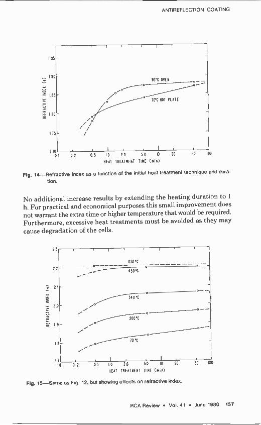
Fig. 14-Refractive index as a function of the initial heat treatment technique and dura-
tion.
No additional increase results by extending the heating duration to 1
h. For practical and economical purposes this small improvement does
not warrant the extra time or higher temperature that would be required.
Furthermore, excessive heat treatments must be avoided as they may
cause degradation of the cells.
2.3
2.2 O -
I
650°C
450°C o o
2.1 - 0- -, 340 °C
2.0 /o /0- - 200°C
1.9r /o !
1.8- i0 10°C
o-1
IT .1 0.2 0.5 1.0 2.0 5.0 10 2°0 50
HEAT TREATMENT TIME (min)
Fig. 15-Same as Fig. 12, but showing effects on refractive index.
IOD
RCA Review Vol. 41 June 1980 157

- 2.3
- 1.5-
` 1.3
/meó
9r'á /p
Oj
soo 'I
ao'49 \%``E\ <-21, O. '1%Q
<17`EQEF
Fig. 16-Same as Fig. 13, but showing effects on refractive index.
Heat treatments in vacuum instead of normal pressure did not in- crease the refractive index or change the film properties to a measureable extent.
Ñ,
VN N
J -e
LI rtN W N r- J
N
N N
-117.40
1
Y
t t v
G- 1
0.45 --T-
Q.50 -rT
0 55
UNCOATED Si SUBSTRATE
670 A RCA-TiO7 ON Si
a 0.5 min 450 C
5.5 min 450 C
55.5 min 450 C
-0° ---1,8=,,.--r
aJ_
1 --1 7.f: 7r 0.E i Q. 7¢ 0, 75
NHVf.!N 14. M1(RGN1 0.P0 0.85
Fig. 17-Absolute reflectance of spray -on TiO2 coatings on silicon as a function of wave- length after a 450°C final heat treatment for various durations. Note that the AR coating is essentially cured after only 30 sec at 450°C.
158 RCA Review Vol. 41 June 1980

ANTIREFLECTION COATING
100
90
80
70
cc - 60
/ 50-\
i
670 * RCA-TiO2 ON Si
0.5 nun 450 C
UNCOATED Si SUBSTRATE
40 3 .4 .5 .6 7 .8 .9 JO
WAVELENGTH X (/.Lm )
Fig. 18-Reflection spectra in terms of (1-R)% vs. wavelength for the silicon sucstrate and
for a 670-A thick TiO2 film on silicon heated for 30 sec at 450°C.
3.3.4 Reflectance, Transmittance, and Absorbance
A computer print-out plot showing absolute reflectance as a function of wavelength of a 670-A thick TiO2 spray -coating on polished silicon slices is presented in Fig. 17. A broad reflectance minimum of 1.3% occurs
in the desired wavelength range of 0.60 to 0.62 pm. The effects of final heat treatments at 450°C for 0.50, 5.5, and 55.5 min shows negligible reflectance differences in the region of the minimum, indicating that the
coating is essentially fully cured after a final heat treatment of only 30
sec at 450°C. A comparative curve for the uncoated polished silicon substrate shows an absolute reflectance of 26 to 27 %D in the wavelength
range of 0.55 to 0.75 pm. Reflection spectra in terms of (1-R)% versus
wavelength for the TiO2 film heated for 30 sec at 450°C, and for the uncoated silicon substrate, are presented in Fig. 18.
On glass substrates (n - 1.5) the same TiO2 films increase the reflec-
tance substantially, as expected (see Fig. 19).
Transmittance curves for the identically -treated coatings on fused
silica substrates are presented in Fig. 20. The data indicate that there is no significant absorption down to a wavelength of 0.35 pm.
RCA Review Vol. 41 June 1980 159

R(4
11 . -
,.-.. s .-. .-.-.-T-<.s-. -.- -. : _._. - 670 A RCA-TiO2 ON GLASS
0.5 min 450 C
5.5 ,n n 450 C
= 55.5 min 450C
N 1
'5,42 0.`r, 0.E0 O.C; AvCLIN";v. MICR;S'
UNCOATED GLASS SUBSTRATE
Zr-2 Z. 7S 0.62 0.85
Fig. 19-Absolute reflectance of the TiO2 films defined in Fig. 17, but on glass substrate, indicating a substantial increase in reflectance compared to that of the uncoated control.
RCA
670 A RCA - TiO2 ON QUARTZ
0.5 min 450 C
5.5 min 450 C
55.5 min 450 C
1
I
0.350 0.50 0.550 0.650 0.750 0.850 0.950 1.050 WAVE;FN_r4. N.;CRqNS
Fig. 20-Transmittance as a function of wavelength for TiO2 films treated as defined in Fig. 17. Measurements were made with reference beam passing through air.
160 RCA Review Vol. 41 June 1980

ANTIREFLECTION COATING
3.3.5 Structure
The structure of TiO2 films was examined by x-ray diffractometry. Films of several thousand angstroms were deposited on fused silica substrates followed by our conventional heat treatment sequence. No crystalline diffraction was recorded on samples heated after the final step at 450°C for 30 sec, indicating an amorphous structure. However, in another test, samples heated for 55 min exhibited the presence of a crystalline phase which was indentified as anatase, the tetragonal form of Ti02.
Infrared absorption spectroscopy (transmission mode) of 6000-A thick films on silicon showed no specific absorbance maxima in the wave number range of 670 to 2700 cm -1 after each of the three heat -treatment steps. A strong absorbance maximum at 3500 cm -1 indicated the pres- ence of OH groups. The intensity of this band decreased with progressive heating treatments from 200 to 450°C, revealing the elimination of hy- droxy groups with thermal curing of the film.
f. .
Fig. 21-SEM micrographs showing particulate agglomerates on the surface (A) and in a
micropinhole (B) of a sprayed -on TiO2 film. Vertical measure of top defect is 1.8
and of bottom defect is 0.6 µm.
RCA Review Vol. 41 June 1980 161

Microscopic inspection of spray -coated TiO2 films usually shows some defects, such as particulate oxide or hydroxide agglomerates and mi- cropinholes. SEM micrographs of a typical defect of each type are pre- sented in Figs. 21A and 13. Electrical measurements of cell efficiency have shown that the presence of such defects does not significantly impair cell performance. Auger electron spectroscopy depth profi es indicated excellent compositional uniformity of the films, regardless of duration of heat treatment at 450°C. Carbon and sulfur were the only impurities detected during this analysis.
A few experiments were carried out to assess the possible merits of laser annealing in addition to, or instead of, the heat treatments of sprayed -on TiO2 coatings. Silicon test wafers and metallized solar cells were subjected to a frequency -doubled Nd-YAG laser beam (0.53 pm, 5K Hz, 100 ns, 100 pm beam diameter) at energy densities ranging from 0.40 to 0.85 J/cm2. The lower energy did not lead to detectable changes in the films, whereas the higher energy density caused vaporization of the films, leaving a relatively clear substrate surface. No further detailed tests were made since the initial results showed little promise.
3.3.6 Corrosion Resistance
An important requirement of the AR coating is its resistance to corrosion, stress relief, delamination, cracking, or chemical changes over an ex- tended time frame. A simple but rigorous functional test that has shown good correlation with long-term degradation of refractory oxide films in field conditions is the hot water test. In this procedure the sample is immersed in boiling distilled water for 10 to 20 min.60 Typical samples of TiO2 spray -on films on polished silicon wafers ani on metallized solar cells were boiled for periods of up to 60 min to simulate exceptionally severe conditions. Ellipsonetric measurements of film thickness and index of refraction showed no change after these tests. The films re- mained clear, without cracks or microscopically visible defects, and did not peel or delaminate on Scotch tape testing, indicating excellent sta- bility.
Abrasion resistance of the spray -on TiO2 films on smooth silicon surfaces is excellent, based on the simple but effective rubber eraser test.
The resistance of the film toward corrosive chemicals was tested by immersing coated silicon wafers and metallized solar cells for one hour at a temperature of 85°C in the following aqueous reagents, all at an absolute concentration of 1 wt%: HCI, HNO:3, H2SO4i H31)04, and NH1OH. No deterioration or visual changes of any sort occurred on the samples during these demanding corrosion tests.
162 RCA Review Vol. 41 June 1980

ANTIREFLECTION COATING
Hardened TiO2 spray -deposited films on solar cells, when subjected to 1-5 vol % aqueous solutions of concentrated HF, are removed in 2 to 5 min with no resultant degradation of cell electrical parameters. Etching is heterogeneous in the sense that a gradual thinning of the layer is often accompanied by undercutting and flaking. Cells may be stripped and recoated with no further surface preparation other than thorough rinsing and drying to eliminate potentially harmful residual HF and mois- ture.
Exposure of sprayed and cured TiO2 films to polyvinylhutyrate plastic at elevated temperature and pressure, as used at RCA in the lamination to glass panels for array assemblies, likewise showed no signs of attack, deterioration, or visual changes.
3.4 Effects on Solar Cell Efficiency
The effects of AR coatings on the electrical performance of solar cells was studied as a function of film thickness for spray solutions prepared from various titanium source materials. These materials included ti- tanium(IV) isopropoxide, titanium(IV) ethoxide, titanium(IV) butoxide, and commercial "Titaniumsilicafilm-C" concentrate. A preliminary test matrix showed that the AR coating obtained from all four sources were of high quality and of similar effectiveness. No advantages were gained by using the butoxide or the more expensive and less stable ethoxide instead of the isopropoxide specified in the RCA-TiO2 spray mixture. The tests to he described in this section were therefore confined to the RCA-TiO2 spray mixture and the spray solution prepared with "Ti- taniumsilica film C."
Throughout the remainder of the paper, All coatings derived from spray mixtures incorporating the commerical "Titaniumsilicafilm-C" concentrate will be referred to as "Si02-Ti02" for brevity and clarity.
The coating experiments were conducted with two types of solar cells for comparison: (1) RCA cells having screen -printed silver metallization and (2) OCLI cells* having conventional evaporated Ti/Pd/Ag metal- lization. The conversion efficiency of cells before and after AR coating was determined by the usual I,, and Vr measurements, as described in Sec. 2.5. 1-V curves for typical cells of each type of metallization are presented in Figs. 22 and 23. The ratio of .1sc measured after AR coating over JS, of the bare cell before coating was taken as a convenient ap- proximation of the change in conversion efficiency under standardized irradiation conditions. Polished single -crystal silicon wafers were used as control substrates for the optical measurements.
Manufactured by Optical Coatings Labs., Inc., Santa Clara, CA.
RCA Review Vol. 41 June 1980 163

L20
1.00
0.80
H 0.60
0.40
0.20
SOLAR CELL NO.107 Ag SCREEN -PRINTED RCA CELL
AR COATING NONE RCA - Ti 02
1st 0.80 1.11 A
Voc 0.570 0.590 V
IM 0.710 0.99 A VM 0.470 0.475 V F. F. 0.732 0.719
8.6 12.1 41 04
AR
- - I -V CURVES
NO AR
INCREASE
- 0.60
-0.40
a - 0.20
0
Fig. 22-Solar cell I -V and power curves before and after RCA-TiO2 AR coating; Ag screen -print metallization.
The results for RCA cells with screen -printed silver metallization, AR -coated with the RCA-TiO2 source solution, are summarized in Table 4. The effect of Ti02 film thickness on the increase in current density ratio I' (J,. after coating/.JR, before coating) is shown graphically in Fig. 24. A broad maximum of I' = 1.39 is attained with a film thickness of 700 A.
Film thickness measurements were done ellipsometrically on the cells as well as on analogously AR -coated polished silicon test wafers. The films on cells gave unreliable thickness readings due to the surface roughness of sawed and chemically etched silicon surfaces. The acurate film thicknesses measured on the smooth test wafers are considered representative and were used for plotting the Js, increase versus thick- ness graphs. (Stylus profilometric traces of typical RCA cell surfaces showed silicon roughness peaks of 0.4 pm at an average frequency of 9 peaks/mm horizontal distance, rendering step -height measurements of
164 RCA Review Vol. 41 June 1980
ANTIREFLECTION COATING
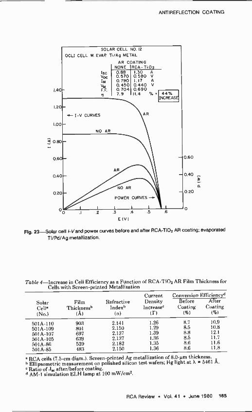
1,40-
SOLAR CELL NO. 12
OCLI CELL W. EVAP Ti/Ag METAL
AR COATING
Isc voc IM
VM F. F.
NONE 0.88 0.570 0.790 0. 450 0.704 7.9
1.20-
1.00 -
a 0.e0^
0.60 -
0.40 -
0.20 -
RCA- Ti02 1.30 A 0.580 V 1.17 A
0.440 V 0.690 11.4 %
AR
NO AR
POWER CURVES -+
I t I l I
.1 .2 .3 .4 .5
Elv)
44% INCREASE
- 0.60
-0.40
- 0.20
0
a.
Fig. 23 -Solar cell l-Vand power curves before and after RCA-TiO2 AR coating; evaporated
Ti/Pd/Ag metallization.
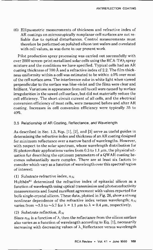
Table 4 -Increase in Cell Efficiency as a Function of RCA-TiO2 AR Film Thickness for Cells with Screen -printed Metallization
Current Conversion Efficiencyd
Solar Film Refractive Density Before After Cells Thicknessl' Index1' Increase° Coating Coating (No.) (A) (n) (I') (%) (%)
501A-110 903 2.141 1.26 8.7 10.9
501A-109 801 2.150 1.29 8.5 10.8
501 A-107 697 2.137 L39 8.8 12.1
501A-105 639 2.137 1.36 8.5 11.7
501A-86 539 2.182 1.35 8.6 I 1.6
501A-85 483 2.150 1.36 8.6 11.8
RCA cells (7.5 -cm diam.). Screen -printed Ag metallization of 8.0-µm thickness. I' Ellipsometric measurement on polished silicon test wafers; Hg light at A = 5461 A.
Ratio of after/before coating. d AM -1 simulation ELH lamp at 100 mW/cm2.
RCA Review Vol. 41 June 1980 165

1.50 EFFICIENCY INCREASE VS. FILM THICKNESS
RCA Ag SCREEN -PRINTED METALIZATION, RCA - TiO2 COATED
.40- - o
.30
.20
1.10
.00-- - 1
500
o
UNCOATED CELLS
l I
600 700 FILM THICKNESS (A)
I
800 900
Fig. 24-Electrical performance as a function of AR film thickness. Cells have a 8 -pm thick screen -printed Ag metallization grid.
the thin AR film also unreliable.) The ellipsometrically determined index of refraction averaged 2.15 for the test wafers and 2.18 for the cells.
The cell conversion efficiency n averaged 8.6% before and 11.5% after TiO2 coating. Comparison with a vacuum -evaporated Zr02 AR coating of similar film thickness (725 Á) and refractive index (n = 2.0) showed improvements of only a few percent in efficiency despite the perfect uniformity of film thickness and absence of any particulate impurities or heat treatments.
The results we obtained for OCI.I cells with 2.7 -µm -thick vacuum - evaporated Ti/Pd/Ag metallization are presented in Table 5 and in Fig. 25. The effectiveness of the OCLI sputter -deposited SiO,r AR coating was determined by measuring the current density before and after chemical stripping of the coating. As indicated in Fig. 25, the ratio in- crease (I') averaged 1.45 for a nominal ellipsometric film thickness range of 820 to 870 Á. No test wafers with SiOx were available for comparison. The cell conversion efficiency averaged 7.6% for hare cells and 11.0% for SiOx coated cells for an optimized film thickness range within 820-870 Á.
Recoating the cells with RCA-TiO2 led to a peak increase of r of at least 1.48, centered between 625 and 675-A film thickness. Recoating with Si02-TiO2 led to a I' maximum of 1.42 for a film thickness bet ween 700 and 740 Á. The film thicknesses stated were obtained from ellipso-
166 RCA Review Vol. 41 June 1980

ANTIREFLECTION COATING
Table .5 -Increase in Cell Efficiency as a Function of AR Film Thickness for Cells with Evaporated Metallization
Solar Cell' (No.)
Film 'I hicknessei
(A)
Current Refractive Density
Indexe' Increaser In (r)
Conversion Efficiency4 Before Coating
1%)
After Coating
(%)
Spray -Liquid RCA-TiO2 10 895 2.220 1.38 7.6 10.6
11 745 2.21)4 1.44 7.6 10.8
12 677 2.19:1 1.48 7.9 11.4
9 605 2.218 1.46 7.4 10.8
7 545 2.187 1.41 7.8 11.1
8 515 2.165 1.10 7.4 10.3 SiOs-TiO2
I 940 1.9-3 1.38 7.3 10.2
2 816 1.950 1.39 7.6 10.6 3 745 1.940 1.42 7.4 10.0
1 702 1.929 1.-12 7.8 10.9
6 604 1.9:13 1.39 7.4 9.9 5 572 1.916 1.38 7.6 10.3
( )CI.I cells (7.5 cm diam.). Vacuum -evaporated '1'i/I'd/Ag metal Iizat ion: cells st ripped of their original SiO% AR coating. Profilometrically measured metal thickness is 2.7 m. ' EIlipsometric measurement on polished silicon test wafer: Hg light at A = 5461 A. r Ratio of.Ir after/before recoat ing. d AM -1 simulation E1,H lamp at 100 m\\/cm2.
1.50 w r a o Z
1.20
w ui a
RCA - Ti02 o Si0z-TiQ A SiOa
EFFICIENCY INCREASE VS. FILM THICKNESS
Ti / Pd /Ag EVAPORATED METALLIZATION THREE AR COATINGS
1.10- u Z_
UNCOATED CELLS
1.00 ----- ------------ 500 600 700 800 900
FILM THICKNESS (A)
1000
Fig. 25 -Electrical performance as a function of AR film thickness. Cells have 2.7-µm thick
vacuum -evaporated Ti/Pd/Ag metallization.
RCA Review Vol. 41 June 1980 167

metrically measured silicon test wafers. Measurements on cells again deviated, but in the opposite direction than observed for RCA cells; OCLI cells averaged 17% less than the test wafers. Stylus profilometry indi- cated a cell surface roughness of typically 0.6 pm with a frequency av- eraging 14 peaks/mm horizontal distance.
Fllipsometric measurements of the refractive index of the AR films also gave differences between test wafer substrates and OCLI cells. RCA-TiO2 averaged an index of 2.20 on test wafers and "2.37" on cells; SiO2-TiO2 was 1.94 on test wafers and "2.26" on cells; OCLI SiOx mea- sured "1.81" on cells, which corresponds to normalized values of 1.55 to 1.69 on test wafers. The OCLI cell conversion efficiency averaged 7.6% without AR coating, 10.8% with RCA-TiO2, and 11.0% with OCLI-SiOx. The values for SiO2-TiO2 are somewhat lower, averaging 10.3%. Several statements can be made based on these observations:
(1) Comparison of the effectiveness of RCA -Tí02, SiO2-TiO2, and SiOx AR coatings on commercial thin-film metallized cells showed that TiO2 from RCA-TiO2 solution is superior to both SiO2-TiO2 and OCLI-SiOx, as seen from the maximal 1' values, which are 1.48+ at 625 to 675 A, 1.42 at 700 to 740 A, and 1.45 at 820 to 870 A, respec- tively.
(2) Screen -print metallized RCA cells with RCA-TiO2 coating exhibited a maximal I' value of 1.39 at 700 A. This apparently lower value is due to the higher initial cell conversion efficiency of uncoated RCA cells (8.6%) than that of OCLI cells with coating removed (7.6%). However, the final conversion efficiency after coating increased to 11.5% for RCA cells, but to only 10.8% for OCI.I cells.
(3) The conversion efficiency for OCLI cells recoated with RCA-TiO2 exhibited a maximum efficiency of 11.4% for a film thickness of 700 A.
(4) Although a greater effectiveness should he expected for a physically vapor -deposited AR coating, the conversion efficiency for OCLI cells with their more expensively produced SiOx coating averaged 10.9% for the presumably optimal thickness of these films. Reduced scat- tering losses should result from the more uniform coverage atainable, especially in comparison to the thick -film metallized cells as used in this analytical study.
(5) The results we obtained again emphasize the relative noncriticality of the AR film thickness. For example, the cell efficiency of RCA- 'l'i02 recoated OCLI cells, averaged over the entire tested film thickness range from 500 to 900 A, is a remarkable 10.8% (without indications of drastic decreases beyond this range), as compared to 11.4% for the maximum at about 700 A.
168 RCA Review Vol. 41 June 1980
ANTIREFLECTION COATING
(6) Ellipsometric measurements of thickness and refractive index of AR coatings on microscopically nonplanar cell surfaces are not re- liable due to optical disturbances. Control measurements must therefore be performed on polished silicon test wafers and correlated with cell values, as was done in our present work.
Pilot production spray processing was carried out successfully with over 2000 screen -print metallized solar cells using the RCA-TiO9 spray mixture and the conditions we have specified. Typical cells had an AR coating thickness of 700 A and a refractive index of 2.2. The film thick- ness uniformity within a cell was estimated to he within ±5% over most of the cell surface area. The interference color in white light when viewed perpendicular to the surface was blue -violet and the films were clear and brilliant. Variations in appearance from cell to cell were caused by surface irregularities in the sawed cell surface, but did not materially reduce the cell efficiency. The short-circuit current of all cells, and the electrical conversion efficiency of most cells, were measured before and after AR coating. Increases in cell conversion efficiency were typically 35 to 40%.
3.5 Relationship of AR Coating, Reflectance, and Wavelength
As described in Sec. 1.3, Eqs. 111, [2], and 131 serve as useful guides in
determining the refractive index and thickness of an AR coating designed for minimum reflectance over a narrow band of wavelengths. However, with respect to the solar spectrum, whose wavelength distribution for Si photovoltaic applications varies from 0.3 to 1.1 pm, the physical sit- uation for describing the optimum parameters of a QWAR coating be- comes substantially more complex. There are at least six factors to consider which vary as a function of wavelength over this spectral region of interest:
(1) Substrate refractive index, ns; Hulthén61 determined the refractive index of epitaxial silicon as a
function of wavelength using optical transmission and photoconductivity measurements and found excellent agreement with values reported for bulk single -crystal silicon. These data, plotted in Fig. 26, show a strong nonlinear dependence of the refractive index versus wavelength; Sin
varies from X3.5 to -5.7 for X = 1.1 pm to X = 0.4 pm, respectively.
(2) Substrate reflection, Rsr Since ns; is a function of X, then the reflectance from the silicon surface also varies as a function of wavelength according to Eq. [I I, necessarily increasing with decreasing values of ,\.,Reflectance versus wavelength
RCA Review Vol. 41 June 1980 169

6.0
5.5
5.0 -
-c 4.5-
W zo 4.0-
2.5 -
SILICON
T102 (ORGANOMETALLIC
SOURCE)
3.5
2.0
2.0 - -
0.1 0.3 0"5 0.i 7 0"9 1.1 1"3 1.5
WAVELENGTH ( p.m )
Fig. 26-The refractive index of epitaxial and bulk single -crystal silicon (upper curve) and titanium dioxide (lower curve) increase as a function of decreasing wavelength from \ = 1.1 pm to ñ = 0.3 pm.
for a silicon surface in air (n2 = 1) and under cover (n2 = 1.5) is plotted in Fig. 27.
(3) AR coating refractive index, nor.
The refractive index of the AR film itself varies as a function of wave- length. Haigh28 published relevant data for TiO2 AR coatings from an organometallic source by ellipsometric techniques and showed nar to increase with decreasing wavelength as shown in Fig. 26 (dashed ex- trapolation is ours).
(4) Solar spectral energy, E,,
Solar irradiance for AM = 0 peaks in the blue region of the visible spectrum. The overall energy is reduced at all wavelengths after passing through the earth's atmosphere because of scattering, absorption of the UV by ozone, and absorption of the near IR by water vapor, CO2, and other gases. The peaks for AM = 1 and AM = 2 shift to longer wave- lengths and are much broader, as shown in Fig. 28.62
170 RCA Review Vol. 41 June 1980

ANTIREFLECTION COATING
50
° 45 W U 4 (1 4C co
Z o - 35 _J
N
o 30 cr
w U á 25
u w J w 20 cr
15 0.1
n2=1.0(AIR)
n2=1.5 (COVER)
0.3 0.5 0.7 0.9 11.1
WAVELENGTH (µm) 1.3
Fig. 27-The reflectance from a silicon surface in air and under cover substantially increases
with decreasing wavelength over the range shown.
(5) Spectral response, S.R.
Because of the nonlinear relationship among absorption coefficient, wavelength, and the minimum ionization energy (1.1 eV for Si), the sil- icon solar cells' ability to collect an electron-hole pair is also a function of wavelength, and generally exhibits a broad maximum near X --- $).7µm.
Infrared photons having a wavelength longer than 1.1 pm cannot release an electron-hole pair, and photons in the visible and ultraviolet parts of the spect rum have excess energy which merely generates heat resulting in a reduction of energy efficiency hut not quantum efficiency. Also, wavelength determines the depth at which electron-hole pairs are gen- erated within the cell, which in turn influences the collection efficiency. The spectral response of cells with an arsenic -diffused junction used in
our investigation is presented in terms of relative quantum efficiency ín Fig. 29.63
(6) AR coating reflection, R(1wAr,
Application of a quarter -wave AR coating to the silicon surface produces a minimum reflectance for a narrow band of wavelengths with increasing reflectance at either side. Fig. 17 depicts absolute reflectance versus wavelength for our spray -on TiO2 coatings.
This complex physical situation is described graphically in Fig. 30.
With respect to determining the optimum parameters of an AR coating
RCA Review Vol. 41 June 1980 171

50. 1020
7440
30
10
AM -2
(, I I1. 1 i.1_1 11 11 l .3 4 5 .6 .7 .8 .9 I O I I 12
WAVELENGTH (MICRONS)
Fig. 28-Solar irradiance in terms of photon flux. Peaks for AM =1 and AM = 2 are broader and shift to longer wavelengths.
1.0
0.8
0.6
0.4
0.2
0 0.4 0.5 0.6 0.7 0.8 09 1.0 II
WAVELENGTH (µm)
Fig. 29-The Spectral response in terms of relative quantum efficiency for an arsenic -dif- fused Si junction
i
172 RCA Review Vol. 41 June 1980

ANTIREFLECTION COATING
o cr 50r _, wi I
Z 40Ir a I
I- 2 301- J w w I
¢ 201-
1.0r 0.91-
0.81-
07- 0.61-
0.51-
0.41-
0 3r 0 2- 01 oL
3000
2500
2000
1500
1000
Rc=34 %
Ro =50%
nsi'5.67
20%
38% 35%
4.20I I 3.90
17% 17% 16%
I
33% 32% 3r%
I I
3.65 3.57 3.l 53
\ 1/ \' 500 - A
R owaa \ '
1 `' I' I 1 ! ...'" 0.3 0.4 0.5 0.6 0.7 08 0.9 1.0 I.I
WAVELENGTH (µm)
S. i 1
1.2
Fig. 30-Graphical analysis of n$1, R51, E S.R, and ROWAR as a function of wavelength for determining the optimum parameters of an AR coating over the wavelength range A = 0.3 to 1.1 pm. Simultaneous evaluation of these curves and the associated data indicated is necessary for determination of T/ at any particular wave- length.
on silicon, superimposed curves and associated data of these factors are plotted as a function of wavelength. The solar spectral energy values (Es, in terms of mW cm -2µm-1) were obtained from the Energy Technology Handbook6 ; absorption minima have been omitted to avoid congestion. To permit comparison, the spectral response (S.R.) in terms of relative quantum efficiency of the silicon cell in Fig. 29 was recalculated in terms of mA nW-1. The reflectance curve (RgwAi) was determined from an experimentally optimized QWAR coating of spray -on TiO2 of Tf = 680 A and ne,. = 2.2 as determined in 6328-A light. Above these curves of Es, S.R. and RtfwAn versus wavelength, values of the refractive index of silicon (ns; ), the reflectance (R0) of the silicon in air, and the reflectance (Re) of the silicon under cover (n2 = 1.5) have been tabulated at different intervals along the solar spectrum.
Examination of these data in Fig. 30 will give some indication as to the degree of difficulty in determining the optimal thickness and re- fractive index of a QWAR coating, but some interesting conclusions can he drawn. A considerable number of high-energy photons near A = 0.45 pm are lost due to the high reflectance (^-45% in air and -'30% under cover) and the low spectral response (--0.2 mA mW-') of silicon. This loss is further compounded by a high absolute reflectance (^-23%) of the QWAR coating. Basically the same argument exists at lower energies near A = 0.9 pm, but to a lesser extent. A dual anti reflection coating could
RCA Review Vol. 41 June 1980 173

extend the minimum reflectance of the QWAR coating out to higher energies, but the low spectral response coupled with the necessity of an inordinately high refractive index (n á 2.8 at Ari = 6000 A) of the layer adjacent to Si, not to mention the added processing cost, makes this procedure questionable. An extensive theoretical treatment of AR coatings on solar cells by Gandham, et al.5° corroborates our conclusions, which are based on experimental results. (High -efficiency concentra- tor -type cells are an exception; they do require a multilayer AR coating for maximum effectiveness.65)
The ideal refractive index of an AR coating to achieve maximum ef- fectiveness across the solar spectrum is a strong function of wavelength (similar to that of silicon in Fig. 26) and follows the relationship in Eq. 121. Fig. 31 shows the ideal values of refractive index versus wavelength for optimum QWAR coatings on silicon in air and under cover. Assuming that silicon cells will be protected with a plate of silicate glass (n2 = 1.5), in actual use, the highest possible value of pia, should be attained. At A
= 0.6 µm, for which most coatings are tuned to obtain minimum reflec- tance (R,;) from the silicon surface, the index requirement from Fig. 31 is nar 2.4. Unfortunately no readily depositahle films possess such a high refractive index with good transmission.
3.0
2.5
2.0
15 0.1
WITH COVER (n2=1.5)
IN AIR (n2=1.0)
I I I ! I
0.3 0.5 0.7 0.9 1.1 1.3
WAVELENGTH (µm)
1.5
Fig. 31-Ideal values of the refractive index versus wavelength for optimum QWAR coatings in air and under cover as computed from refractive index values of silicon in Fig. 11.
174 RCA Review Vol. 41 June 1980

ANTIREFLECTION COATING
The optimum thickness (T1) for a QWAR coating on a silicon solar cell requires the simultaneous evaluation of the several previously mentioned parameters, graphically illustrated in Fig. 30. Assuming nay
to he fixed for a particular coating material, any attempt to predict the thickness for maximum broadband antireflection must include an analysis of nl;, Rs;, Es, S.R., and RQwAR as a function of wavelength. We
believe the best and simplest way to obtain the optimum thickness value is experimentally, as shown in the examples in Figs. 24 and 25.
The tolerances for attaining the optimum thickness are relatively wide.
For example, across the 400-A spread of AR coating thicknesses in Fig.
24, the maximum J at T1 - 590 A represents only a 4 to 9% increase from those of 500 A and 9(X) A, respectively. Shah and Fuller29 presented similar curves for arsenic -doped oxide AR coatings (nor 1.5) on both P- and As -diffused silicon cells which have shown even less sensit ivity of the Jse to thickness variations. Cells with large off -optimum thick- nesses (-15%) of spray -on TiO2 can still function adequately with only a 3 to 5% decrease in J, which represents a minor decrease (-0.5%) in the overall efficiency (r]) of the cell, since most of the Jsc is already present before AR coating. The main point to be noted is that the ±15% off -optimum AR coated cell still produces -95% of the electrical energy which it is capable of producing with an optimum thickness.
The wide tolerance in the AR coating thickness explains why defects normally encountered in the spray process, such as particulates and lo-
calized thickness irregularities (especially along the thick. screen -sprinted
metallization), are not a problem. These defects are essentially cosmetic in nature and have a minimal effect on the overall efficiency of the cell. The small increase in total efficiency obtainable by AR coatings from expensive vacuum techniques is more than offset by the low-cost, high-speed spray technique which is compatible with a high degree of automation for mass production.t's
4. Conclusions
(1) A high-speed mass production process has been developed and optimized for depositing, at low cost, a single -layer, thin-film an- tirellection coating on metal -patterned single -crystal silicon solar cells for terrestial applications. The process has been applied suc- cessfully to cells with either evaporated Ti/Pd/Ag metallization on a polished silicon surface or screen -printed silver metallization on a saw cut and etched silicon cell surface.
(2) Several materials and deposition methods have been examined for
producing the AR coating. The film material selected was titanium
RCA Review Vol. 41 June 1930 175
dioxide. We have prepared this compound by automated atom- izat ion spraying of titanium(IV) isopropoxide in a liquid organic solution. After drying, the film is reacted ín air by a series of heat treatments to form TiO2.
(3) Several organotitanium compounds were tested as sources for preparing the spray mixture, including titanium(IV) isopropoxide, titanium(IV) ethoxide, and titanium(V) butoxide. The commercial "Titaniumsilicafilm C" concentrate was also tested for preparing the spray solution, but was expensive and did not lead to superior cell performance. Titanium(IV) isopropoxide was found to be the preferred material, from both technical and economic consider- ations.
(4) The composition of the spray solution was devised and optimized to yield a uniform film of accurately controllable properties. Vapor pressure, viscosity, miscibility, chemical reactivity, and surface tension of the solution components were among the critical char- acteristics of the mixture components. In addition to the titani- um(IV) isopropoxide as the essential reactant, n -butyl acetate is used as the diluent solvent to form a single-phase solution. A low - molecular weight aliphatic alochol, preferably sec-butanol, serves as a leveling agent to spread the solution uniformly between the metallization grids. A key component for rendering the solution successfully sprayable by optimizing critical physical and chemical mixture parameters is 2-ethyl-1-hexanol; it allows the attainment of a continuous and uniform liquid film.
(5) Atomization spraying of the organotitanium spray solution uses commercial automated equipment of refined design, having the capability of controlling the deposition parameters precisely. Spraying is conducted in air of controlled purity and at low relative humidity level to avoid premature reaction in the gas phase. Three machine parameters were selected from about 15 to vary and con- trol the film thickness: (1) source solution delivery pressure, (2) atomization spray pressure, and (3) gun -to -substrate distance.
(6) A series of brief post -deposition heat treatments in room air are applied at 70°C, 200°C, and 450°C, respectively, to form the final TiO2 AR coating. The cured films consisted essentially of amor- phous TiO2, had a refractive index in the range of 2.1 to 2.2, and were readily removable with hydrofluoric acid. A 670A thick film on a polished silicon substrate exhibited a reflection minimum of 1.3% (absolute) at a wavelength of 0.60 pm. Films on plates of fused quartz showed no significant light absorption down to a wavelength of 0.35 pm.
176 RCA Review Vol. 41 June 1980
v

ANTIREFLECTION COATING
(7) The uniformity of film thickness on metallized and spray -coated solar cells was better than 15% over the major portion of the cell surface. We demonstrated that the TiO2 film thickness in the range of 600 to 750A is non -critical in terms of cell efficiencies.
(8) The TiO2 AR coating adheres well and is extremely stable and corrosion resistant, as demonstrated by exposure of coated cells to boiling water and to hot diluted acids and ammonia.
(9) Application of the process to the coating of over 2000 single -crystal 7.5 cm -diameter solar cells with either screen -printed silver me- tallization or with vacuum -evaporated Pd/Ti/Ag metallization showed increases of over 40% in the electrical conversion effi- ciency.
(10) Based on an annual production rate of 55 million cells capable of yielding 30 million watts electrical power, the cost for producing the antireflection coating by this process is at present only one cent per cell, or less than 2 cents per watt. This amount is less than one -eighth of that for conventional vacuum sputtering. The out- standing advantage of' the spray deposition process is its ideal suitability for continuous automated mass production of solar cells. The process has been evaluated and verified for application by .let Propulsion Laboratory.
(11) Finally, the optics underlying AR coatings have been reviewed and consideration for optimizing AR coatings for photovoltaic cells have been discussed. It was shown that the thickness of'the film is rela- tively noncritical over a considerable range, which agrees with our experimental results. In addition, a comprehensive literature search covering over 50 references on the subject of AR coating for solar cells has been presented.
Acknowledgments
We wish to thank W. Kurylo for his contribution to the spray coating and processing of over 2000 solar cells, R. V. D'Aiello for testing and evaluating coated cells, G. E. Nostrand for electrical characterization measurements, J. C. Toner for computer programming comparative cost analyses, and P. J. Zanzucchi for optical measurements. We aLso ac- knowledge the guidance we received from C. Brell of Zicon Corporation in regard to spray machine parameters. Thanks also to G. L. Schnable, A. H. Firester, J. P. Wittke, and R. V. D'Aiello for critically reviewing the manuscript.
References:
' G. Cheek, A. Genis, J. B. DuBow, and V. R. Pai Verneker, "Antireflection Properties of Iridium Tin Oxide (ITO) on Silicon For Photovoltaic Applications," Appl. Phys. Lett., 35, p. 495, Oct. 1979.
RCA Review Vol. 41 June 1980 177

2 B. E. Yoldas and T. W. O'Keeffe, "Antireflective Coatings Applied From Metal-Organic Derived Liquid Precursors." Applied Optics, 18, p. 3133, Sept. 1979.
3 T. Feng, A. K. Ghosh, and C. Fishman, "Spray -Deposited High -Efficiency Sn02/n-Si Solar Cells," Appl. Phys. Lett., 35, p, 266, Aug. 1979. 4R. B. Godfrey and M. A. Green, "655 mV Open -Circuit Voltage, 17.6% Efficient Silicon MIS Solar
Cells," Appl. Phys. Lett., 34, p. 790, June 1979. 5 W. A. Anderson and J. K. Kim. "Reliability Studies on MIS Solar Cells," Appl. Phys., 17, p. 401, Dec.
1978. 6 J. Michel, E. Fabre, M. Mautret, and P. Mas, "Reflectivity Analysis on Silicon Solar Cells," 13th IEEE
Photovoltaic Specialists Conference, p. 1244, Washington DC, June 1978. 7 T. L. Chu, S. S. Chu, E. D. Stokes, C. L. Lin, and R. Abderrassoul, "Thin Film Polycrystalline Solar
Cells," Ibid., p. 1106.
8 Y. C. M. Yeh, F. P. Ernest, and R. J. Stirn, "Progress Towards High Efficiency Polycrystalline Thin -Film GaAs AMOS Solar Cells," Ibid. p. 966.
9 S. S. Chu, T. L. Chu, and H. T. Yang, "Large Area Thin Film Gallium Arsenide Solar Cells," Ibid., p. 956. 10 J. C. C. Fan and C. O. Bozler, "High Efficiency GaAs Shallow Homojunction Solar Cells," Ibid. p. 953. 11 A. Meullenberg, Jr., "Space Environment Damage to Solar Cell Coverslide Assemblies," Ibid. p. 107. 12 E. Bucher, "Solar Cell Materials and Their Basic Parameters," Appl. Phys., 17, p. 1, 1978. 13 H J. Hovel, "TiO2 Antireflection Coatings by a Low Temperature Spray Process," J. Electrochem. Soc., 125, p. 983, July 1978. 14 S. S. Chu, T. L. Chu, and H. T. Yang, "Thin -Film Gallium Arsenide Solar Cells on Tungsten/Graphite Substrates," Appl. Phys. Lett., 32, p. 557, May 1978. 15 D. H. Olson, "Silicon Monoxide Antireflection Coatings for InP/CdS Solar Cells," J. Va. Sci. Technol., 15, p. 130, Jan. -Feb. 1978. 16 P. Van Helen, R. Mertens, R. Van Overstraeten, R. E. Thomas, and J. Van Meerbergen, "Improvement of the Efficiency of Silicon MIS -Inversion Layer Solar Cells," Proc. International Cont. on Photovoltaic Solar Energy, p. 280, Luxemburg, Sept. 1977. 17J. F. Gibbons and F. C. Wu, "Fabrication and Measurement of Silicon Concentrator Solar Cells," Ibid., p. 242. 18 W. G. Townsend and D. R. Lillington, "Progress on Aluminum P -Type Silicon SBSCS," Ibid., p. 207. 19 G. A. Swartz, L. S. Napoli, and N. Klein, "Silicon Solar Cells Ior Use at High Solar Concentration," IEEE International Electron Devices Meeting, p. 226, Wash. DC, Dec. 1977. 20 R. J. Stirn, Y. C. M. Yeh, E. Y. Wang, F. P. Ernest, and C. J. Wu, "Recent Improvements in AMOS Solar Cells," Ibid. p. 48. 21 P. A. Iles, "Antireflection Coatings for Solar Cells," J. Vac. Sci. Technol., 14, p. 1100, 1977. 22 K. W. Mitchell, A. L. Fahrenbruch, and R. H. Bube, "Evaluation of the CdS/CdTe Heterojunction Solar Cell," J. Appl. Phys.. 48, p. 4365, 1977. 23 S. Franz, G. Kent, and R. L. Anderson, "Heterojunction Solar Cells of SnO2/Si," J. Electron Mater. 6, p. 107, 1977. 24 H. Matsunami, S. Matsumoto, and T. Tanaka, "MIS Solar Cells with In2O3 Antireflective Coating," Jpn. J. Appl. Phys., 16, p. 149, Aug. 1977. 25 H. W. Brandhorst, Jr., "Status of Silicon Solar Cell Technology," Jpn. J. Appl. Phys., 16, Suppl. 1, p. 399, 1977. 26 K. S. Sree Marsha, K. J. Bachman, P. H. Schmidt, E. G. Spencer, and F. A. Thiel, "n -Indium Tin Oxide/p-Indium Phosphide Solar Cells," Appl. Phys. Lett., 30, p. 645, June 1977. 27 D. E. Carlson, C. R. Wronski, A. R. Triano, and R. E. Daniel, "Solar Cells Using Schottky Barriers on Amorphous Silicon," 12th IEEE Photovoltaic Specialists Conf., p. 893, Baton Rouge, LA, Nov. 1976. 28 A. D. Haigh, "Fired Through Printed Contacts on Antireflection Coated Silicon Terrestial Solar Cells," Ibid. p. 360. 28 P. Shah and C. R. Fuller, "High Performance, Inexpensive Solar Cell Process Capable of a High Degree of Automation," Ibid. p. 286. 30 M. G. Coleman, W. L. Bailey, and R. A. Pryor, "Processing Ramifications of Textured Surfaces," Ibid. p. 313. 31 W. A. Anderson, S. M. Vernon, A. E. Delahoy, J. K. Kim, and P. Mathe, "Factors Which Maximize the Efficiency of Cr-p-Si Schottky (MIS) Solar Cells," J. Elecirochem. Soc., 123, p. 1514, Oct. 1976.
178 RCA Review Vol. 41 June 1980

ANTIREFLECTION COATING
32 Y. C. M. Yeh, F. P. Ernest, and R. J. Stim, "Practical Antireflection Coatings for Metal -Semiconductor Solar Cells," J. Appl. Phys., 47, p. 4107, Sept. 1976. 33 A. G. Revesz, J. F. Allison, and J. H. Reynolds, "Tantalum Oxide and Niobium Oxide Antireflection Films in Silicon Solar Cells," Comsat Tech. Rev., 6, p. 57, 1976. 34 A. G. Revesz, J. H. Reynolds, and J. F. Allison, "Optical Properties of Tantalum Oxide Films on Silicon," J. Electrochem. Soc., 123, p. 889, July 1976. 35 H. W. Brandhorst, Jr., "Current Status of Silicon Solar Cell Technology," International Electron Devices Meeting (Technical Digest), p. 331, Wash., Dec. 1975. 36 J. F. Allison, R. A. Arndt, and A. Meulenberg, "A Comparison of the COMSAT Violet and Non -reflective Cells," 10th Intersociety Energy Conversion Engineering Conf., p. 1038, Newark, Delaware, Aug. 1975.
37 Y. M. Yeh and R. J. Stirn, "Improved Schottky Barrier Solar Cells," 11th IEEE Photovoltaic Specialists Conf,, p. 391, Scottsdale, Arizona, May 1975.
38 E. L. Ralph, "Recent Advances in Low Cost Solar Cell Processing," Ibid. p. 315.
39 A. Meulenberg, J. F. Allison, R. A. Arndt, and J. G. Haynos, "Radiation Damage to the COMSAT Non -Reflective Cell," Ibid., p. 204. 4o G. S. Goodelle, G. R. Brooks, and J. R. Mosher, "High Vacuum U. V. Test of Improved Efficiency Solar Cells," Ibid., p. 184.
41 T. Matsushita and T. Mamine, "A New Class of Solar Cell with Multi -Layer Structure." International Electron Devices Meeting (Technical Digest) p. 353, Wash. DC, Dec. 1975. 42 Y. C. M. Yeh and R. J. Stirn, "Practical Anti -Reflection Coating for Metal Semiconductor Solar Cells," Proc. Society of Photo -Optical Instrumentation Engineers, 68, Optics in Solar Energy Utilization. p. 172,
1975. 43A.
G. Revesz, "Vitreous Oxide Antireflection Films in High Efficiency Solar Cells," 10th IEEE Photo- voltaic Specialists Cont., p. 180, Paolo Alio, CA, Nov. 1973.
44 E. Y. Wang, F. T. S. Yu, V. L. Simms, H. W. Brandhorst, Jr., and J. D. Broder, "Optimum Design of Antireflection Coating for Silicon Solar Cells," Ibid., p. 168. 45 W A. Anderson, A. E. Delahoy, and R. A. Milano, "An 8% Efficient Layered Schottky Barrier Solar Cell," Ibid., p. 168. 46 W. A. Anderson and A. E. Delahoy, "Advances in Schottky Barrier Solar Cell Technology," 8th In- tersociety Energy Conversion Engineering Cool. Proc., p. 326, Philadelphia, PA, Aug. 1973. 47 V. Magee, H. G. Webb, A. D. Haigh, and R. Freestone, "Design and Practical Aspects of Maximum Efficiency Silicon Solar Cells for Satellite Applications," 9th IEEE Photovoltaic Specialists Conf., p.
6, Silver Springs, MD, May 1972. 48 P. M. Stella and H. Somberg, "Integrally Covered Silicon Solar Cells," Ibid., p. 179.
a9 I. Chambouleyron and E. Saucedo, "Properties of Chemically Sprayed SnO2 Antireflecting Films on Si Solar Cells," Solar Energy Materials. 1, p. 299, 1979. Sob Gandham, R. Hill, H. A. Macleod, and M. Bowden, "Antireflection Coatings on Solar Cells," Solar Cells, 1, p. 3, Nov. 1979.
51 H. Terui and M. Kobayashi, "Refractive -Index -Adjustable SiO2-Ta2O5 Films for Integrated Optical Circuits," Appl. Phys. Lett., 32, (10), p. 666, May 1978. 52 M. S. Bae and R. V. D'Aiello, "P+/N High Efficiency Silicon Solar Cells," Appl. Phys. Lett.. 31 (4),
p. 285, Aug. 1977. 53 R. A. Arndt, J. F. Allison, J. G. Haynos, and A. Meulenberg, Jr., "Optical Properties of the COMSAT Non -Reflective Cell," 11th IEEE Photovoltaic Spec. Cont., p. 40, 1975. 54 L. H. Hall, "Preparation and Properties of Antireflection Coatings by Chemical Vapor Deposition." J. Appl. Phys., 43 (11), p. 4615, Nov. 1972. 55 I. Mellan, Industrial Solvents Handbook, Sec. Ed., Noyes Data Corp., Park Ridge, NJ. 1977, p. 232 (cited from Union Carbide Corporation). 56 See Ref. 1551, p. 236 (cited from Shell Chemical Co.). 57 H. Schroeder, "Oxide Layers Deposited from Organic Solutions," Phys. of Thin Films, 5, p. 87, G.
Hass and R. E. Thun, Eds., Academic Press, New York, 1969. 58 B. E. Yoldas, "Preparation of Glasses and Ceramics from Metal -Organic Compounds," J. Mater. Sci., 12, p. 1203, 1977. 59 B. E. Yoldas, "Monolythic Glass Formation by Chemical Polymerization," J. Mater. Sci., 14, p. 1843, 1979.
80S. H. Leece, "Function Stress Testing in Large -Scale Optical Multifilm Manufacturing," J. Vac. Sci. Technol., 16 (2), p. 356, March/April 1979. 61 R. Hulthén, "Optical Constants by Epitarial Silicon in the Region 1-3.3 eV," Physica Scripta. 12,
p. 342, 1975.
RCA Review Vol. 41 June 1980 179

62 B. F. Williams, Automated Array Assembly, Quarterly Report No. 3, ERDA/JPL Contract No. 954352-76/3, p. 7, Sept. 1976. 63R. V. D'Aiello, Automated Array Assembly, Phase ll, Quarterly Report No. 3, DOE/JPL Contract No. 954868-78/3, p. 11, June 1978. 64 H. Oman and J. W. Gelzer, in Energy Technology Handbook, Douglas M. Considine, Editor -in -Chief, Chapt. 6, p. 60, McGraw-Hill, Inc., New York (1977). 65 L. S. Napoli, G. A. Swartz, S. G. Liu, N. Klein, D. Fairbanks, and D. Tamutus, "High Level Concentration of Sunlight on Silicon Solar Cells," RCA Review, 38, p. 76, March 1977. 66 W. Kern and C. E. Tracy, "Abstract: Spray -on Antireflection Coatings for Silicon Solar Cells," J. Vac. Sci. Technol., 17, p. 374, Jan./Feb. 1980.
180 RCA Review Vol. 41 June 1980

The Measurement of Deep Centers in Float Zone Silicon by Photovoltage Spectroscopy
L. L. Jastrzebski
RCA Laboratories, Princeton, NJ 08540
J. Lagowski
Massachusetts Institute of Technology, Department of Material Science, Room 13-4130, Cambridge, MA 02139
Abstract-Derivative (wavelength modulated) photovoltage spectroscopy of MOS and MS
structures has been employed for studying band structure transitions and photo -
ionization of deep levels in float zone silicon (p = 2 X 1015 cm -3). From low
temperature (T < 30°K) photovoltage spectra and photovoltage transient char-
acteristics, it has been established that deep levels of the energy 0.56 eV above
the valence band are present in as -grown high quality float zone silicon and in
oxidized wafers. The photovoltage measurements also revealed the presence
of shallow minority carrier traps in the vicinity of the conduction band edge which
is consistent with a noticeable degree of compensation present in the silicon wafers.
1. Introduction
Electrical measurements ín semiconductors provide rather limited in- formation about the origin of deep centers. Nevertheless, they have
proven extremely useful in "labeling" deep levels with respect to the activation energy and the capture cross-section. Such labeling can in turn be used as a basis for establishing the source of process -introduced de- fects,' decoration mechanism of the crystallographic defects,23 and the
RCA Review Vol. 41 June 1980 181

effects of defects in the as -grown material on the device perfor- mance.3'4
A significant practical advancement in characterization of deep levels has been brought about by the development of the Deep Level Transient Spectroscopy (DL'I S).5 DLTS relies on the analysis of the thermal emission of carriers trapped by deep levels and it provides highly sen- sitive means for labeling trapping centers with respect to their thermal activation energy. This technique was successfully used to characterize deep levels introduced to silicon, GaAs, and other semiconductors by radiation damage,6 heavy metals,7 and other impurities.7'8 However, it should he noted that the thermal activation energy measured by DLTS provides sufficient description of the energy level only for the simple trapping centers as defined within Shockley -Read recombination model. In general, the ionization of defect centers may involve absorption (emission) of phonons, lattice relaxation, excited states and/or config- urat ional changes which can be disclosed more easily by optical studies (due to strict momentum and energy conservation rules) than thermal emission.
The photoionization of deep levels has been utilized in conjunction with photocurrent, photocapacitance, or photovoltage measurements. often, however, with much less success than thermal emission DLTS measurements due to ambiguities in determination of photoionization cross-section.
Recently a simple approach has been proposed for the determination of deep -level photoionization characteristics from derivative wavelength modulated photovoltage9 and/or photocapacitance spectra.10 The wavelength modulation utilized in these derivative measurements converts broad photoionization spectra of deep levels into a well-defined peak structure providing a reliable and practical means for labeling of deep levels in the photon energy scale. The advantages of the derivative photovoltage9"l or photocapacitance measurements10 have been dem- onstrated through the band -structure and deep -level studies in GaAs.
In the present study, Derivative Surface Photovoltage Spectroscopy (DSPS) has been applied for the measurement of deep -level and hand - structure transitions in high quality float -zone p -type silicon which is utilized for solid state imagers.'2
The photovoltage measurements showed the presence of the same deep levels in the as -grown and oxidized material, and a procedure to determine their parameters was developed. In addition to the deep centers, the DSPS method also provided information about presence of shallow centers and degree of compensation in the high quality float zone silicon.
182 RCA Review Vol. 41 June 1980

PHOTOVOLTAGE SPECTROSCOPY
2. Derivative Surface Photovoltage Spectroscopy
The surface photovoltage is defined as the change of the surface potential harrier under illumination. There are two mechanisms leading to the
occurrence of the surface photovoltage: (a) the hand-to-hand excitation
of excess carriers and (b) the photoionization of localized levels. The
photovoltage generated in a depletion-space-charge region of p -type
semiconductor is illustrated in Fig. 1. In both instances (i.e., subbandgap
and intrinsic excitation) the photovoltage occurs due to the sepa-ation
of electrons and holes in an electric field within the space -charge region.
In case (h) only the photogenerated holes move in an electric field. The
electrons remain localized in deep levels.
Accordingly, the surface photovoltage can in principle be utilized to
determine the band -structure transit ions and the transitions involving localized levels. The inherently low sensitivity in all standard photo -
voltage configuration has limited such studies to high -energy -gap
semiconductors. Significant extension of the applicability of surface
photovoltage has recently been achieved due to the development of I)SPS.9,'t This new approach combines the advantages of the wavelength
modulation with a strikingly enhanced sensitivity through utilization of the MOS structure.
In the experimental arrangement, schematically shown in Fig. 2, the
surface photovoltage is measured with respect to a transparent, refer -
SPACE CHARGE REGION
(a)
(b)
Et h?Et-Ev
Ev
(-1 (4)
Fig. 1-Schematic representation of the mechanism of photovoltage generated (a) by intrinsic
and (b) by subbandgap illumination (see text).
RCA Review Vol. 41 June 1980 183

semitransparent METAL
ILLUMINATION
11111111 Vltl
OXIDE SEMICONDUCTOR
LOCK -IN
:2
RECORDER
dV, 2 d2V, Vltl.]L da sin 2,,,t -(7) ) cos -...
Fig. 2-Schematic representation of the experimental arrangement for derivative surface photovoltage spectroscopy.
ence, gold electrode evaporated on an oxide layer (500 to 2000 A thick) grown on the semiconductor. With this insulating layer, a sensitivity of 50 'IV can be achieved in the surface photovoltage measurements (i.e., 2 to 4 orders of magnitude higher than previously reported9) permitting the determination of relative changes in the surface harrier as small as about 10-7. Similar measurements can he performed using a Schottky diode as a reference electrode. However, such measurements may be affected by photoinjection of carriers from metal.
In the experimental arrangement of Fig. 2 the periodic wavelength modulation of the incident light generates the photovoltage signal which is analysed directly and through the first- or the second -harmonic phase -sensitive detection. The first- and the second -harmonic detection permit the determination of the first- and second -energy (or wavelength) derivative of the surface photovoltage and thus enable a precise spec- troscopic determination of the energy levels active in photo -induced transitions. The illumination intensity utilized in present measurements was on the level of 1-10 µWatt/cm2, i.e., about seven orders of magnitude lower than in typical photoluminescence studies. The further experi- mental details and the example of an application of the derivative surface photovoltage spectroscopy are given in Ref. [9].
The silicon wafers used for measurements were obtained from com- mercial suppliers (Mansento and Wacker), and they represented the best float zone material with resistivity about 10 ohm -cm (boron doped) presently available on the market. The measurements were performed on the as -grown and oxidized wafers (oxidation done at 900°C ill the steam + NCI). In the case of the oxidized wafers, a transparent layer of gold was evaporated on the oxide to serve as the reference electrode. The Schottky diodes, made by Ti evaporation, were used during measure- ments on the as -grown crystals. The second contact to the samples was
184 RCA Review Vol. 41 June 1980
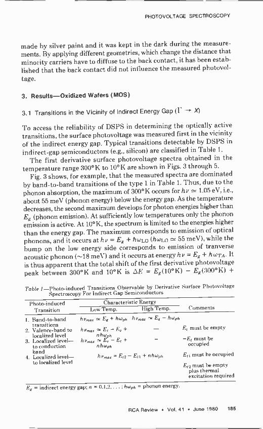
PHOTOVOLTAGE SPECTROSCOPY
made by silver paint and it was kept in the dark during the measure-
ments. By applying different geometries, which change the distance t hat
minority carriers have to diffuse to the hack contact, it has been estab-
lished that the back contact did not influence the measured photovol-
tage.
3. Results-Oxidized Wafers (MOS)
3.1 Transitions in the Vicinity of Indirect Energy Gap (l' X)
To access the reliability of DSPS in determining the optically active
transitions, the surface photovoltage was measured first in the vicinity
of the indirect energy gap. Typical transitions detectable by DSPS in
indirect -gap semiconductors (e.g., silicon) are classified in Table I .
The first derivative surface photovoltage spectra obtained in the
temperature range 300°K to 10°K are shown in Figs. 3 through 5.
Fig. 3 shows, for example, that the measured spectra are dominated
by band -to -band transitions of the type 1 in Table 1. Thus, due to the
phonon absorption, the maximum of 300° K occurs for hi, 1.05 eV, i.e.,
about 55 meV (phonon energy) below the energy gap. As the temperature
decreases, the second maximum develops for photon energies higher than
Eg (phonon emission). At sufficiently low temperatures only the phonon
emission is active. At 10°K, the spectrum is limited to the energies higher
than the energy gap. The maximum corresponds to emission of optical
phonons, and it occurs at hi, = Eg + hcoLo (hwt,0 55 meV), while the
bump on the low energy side corresponds to emission of tranverse
acoustic phonon (--18 meV) and it occurs at energy h i' = Eg + hwTA. It
is thus apparent that the total shift of the first derivative photovoltage
peak between 300°K and 10°K is ,,E = Eg(10°K) - Eg(300°K) +
Table 1-Photo-induced Transitions Observable by Derivative Surface Photovoltage
Spectroscopy For Indirect Gap Semiconductors
Photo -induced Transit ion
Characteristic Energy
Low Temp. High Temp. Comments
1. Band -to -band hvmox EX + ht h h:',, Eg - hWph
transitions 2. Valence -hand to h vm,, E, - Ev + - E, must be empty
localized level nhm h
3. Localized level- h v,,.: ---E' - E, + - -E, must be
to conduction nh0Jph occupied
hand 4. Localized level- hPma, = E,2 - E + nhwph E must be occupied
to localized level E,2 must be empty
plus thermal excitation required
EX = indirect energy gap; n = 0.1,2, ... ; 'mph = phonon energy.
RCA Review Vol. 41 June 1980 185

x19 ----- x15 --- X10
xI
E9 -L0
150 K
180 K
3001N.
1.000
.-. ../"\ ! , j ;
/
Eq(300K) 1
1.100
E9LO
Eq (10K)
: 1.200
PHOTON ENERGY (eV)
1OK
1.300
Fig. 3-First-derivative surface photovoltage spectra of sample Si in the vicinity of indirect band -to -band transitions.
2hco,.o, i.e., it is about three times larger than the temperature shift of the energy gap.
These findings are in excellent agreement with the existing knowledge of the band structure and the phonon spectra of Si,13.14 and they clearly illustrate the reliability of derivative surface photovoltage spectroscopy in the determination of optically active transitions.
From the point of view of impurity related transitions, however, it is of significance to analyze the additional maximum encircled in Fig. 3, which exhibits specific characteristics. As shown in Fig. 4, this maximum is observable only at limited temperature ranges (around 160-130°K for sample S-1 and 130-70°K for sample S-2). Furthermore, it disappears under low -intensity white -light background illumination (see Fig. 5). The latter results indicate that this maximum is related to transitions involving localized levels rather than phonon -assisted hand -to -band transitions. In p -type silicon, low intensity band -to -band generation can not change the occupation of hole (majority carrier) traps; however, it can noticeably increase the occupation of electron (minority carrier) traps. Thus, consistent with the results shown in Fig. 5, the maximum in question can he attributed to transitions of type 2 in Table 1, i.e., to photoionization transitions between the valence band and shallow
186 RCA Review Vol. 41 June 1980

PHOTOVOLTAGE SPECTROSCOPY
130K
142 K
152 K
IBO K
. : 1 1 \1-___I
110 1.15 ' 1.25ev
50K
70 K
90 K
//+ 110K
L-/ 1
1.10 ; 1.15 1.20 1.25ev
Fig. 4-Effect of temperature on transitions in the vicinity of indirect band gap.
electron traps. The fact that these transitions are observed at a limited
temperature range can be explained by considering that at higher tem-
perature, electrons that are photoionized to the localized deep level will
not stay long enough at this level to make a noticeable contribution to
the change of the potential barriers but will he thermally generated to
the conduction band. In this case, the thermal emission will effectively
quench the effect of photoionization. At sufficiently low temperature, on the other hand, the increased value of the time constant of thermal emission (r > 11w) reduces the magnitude of the photovoltaic signal
measured using periodical modulation with an angular frequency, w.
The determination of the energy level E, of electron traps involves
ambiguity due to the unknown order n of phonon replica. An estimate for the value of E, is about 0.05 eV or 0.1 eV below conduction band,
taking at the maximum o = 1 or n = 2, respectively. It is of interest to
note that at a given temperature, the magnitude of the peak in question
was found to vary with changes in the position of the probing area within
a given sample. For sample S-1, e.g., at the central part of the sample,
the peak reached maximum at a T of about 150°K, while at the edges
at a T of about 170°K. Demonstrated sensitivity of this peak to minority
carriers (see Fig. 5) indicates that the differences within a given sample
can he explained as due to local changes of the minority carrier life-
time.
RCA Review Vol. 41 June 1980 187

150 K
1.165 eV
NO BACKGROUND / ILLUMINATION
BACKGROUND r'. / ILLUMINATION
o / / 1, I I/ 1_ -J
1.10 / 1.20 1.25eV
NO BACKGROUND ILLUMINATION
140 BACKGROUND
I t. / ILLUMINATION
l I t`. I
hu = 1.10 / 1.20 L25eV
Fig. 5-Effect of white -light background illumination on transitions in the vicinity of indirect band gap.
3.2 Subbandgap Spectra-Deep Levels
For temperatures below 40°K, a pronounced subband surface photo - voltage was observed that rapidly increased with decreasing temperature. A typical first -derivative spectrum of an MOS structure measured at 10°K is given in Fig. 6.
The fact that the suhbandgap spectra was observed only at low tem- perature is consistent with photoionization transitions involving localized
E11 E9 TA LO
1 I 1 1 1 1 1 1 II 11 1
I:' I
0.5 0.6
x 200 x
0.9 10 I
.\L . I I
7 0.8 '..:...., .... .... ,._ 1.2
PHOTON ENERGY (eV)
Fig. 6-Subbandgap first derivative photovoltage spectra of MOS sample at 10°K.
188 RCA Review Vol. 41 June 1980

PHOTOVOLTAGE SPECTPOSCOPY
levels. In this case, in addition to photoionization transitions, thermal -
generation transitions and recombination (trapping) transitions occur.
Accordingly, photoionization transitions can lead to a measurable change
in the population of localized levels (and thus to a measurable photo -
voltage) only if the thermal generation and the trapping are sufficiently
low. Transitions from deep levels, located around 0.55-0.58 eV, are also
observed in the direct photovoltage spectra (see Fig. 7). A slowly varying
(and thus, not observed in derivative spectra) photovoltage tail at lower
photon energy is also seen ín the spectrum of Fig. 7. It indicates addi-
t ional photoionization transitions involving shallower levels (E,2 < 0.5
eV). However, the optical system employed (hi, >_ 0.50 eV) did not allow
for further identification of these transitions. The higher energy tran-
sitions measured by the DSPS exhibit pronounced oscillatory behavior
(Fig. 6). The oscillatory behavior is analyzed in Fig. 8, where the energy
at the maximum is plotted versus the consecutive number of the maxi-
mum. The slope of the straight line determines the characteristic energy
.SE = 54 f 2 meV, which agrees very well with the longitudinal optical
phonon energy at low temperatures, itwt,o = 55 meV." The interpreta-
tion of the related transitions in terms of the valence -band -localized -
level transitions leads to the energy level E, I = 0.56 eV.
From two possible transitions (i.e., 2 and 3 in Table 1), transition 2
is selected as preferable because transition 3 would require that the levels
0.56 eV below the conduction hand he occupied with electrons, which
ís rather unlikely in p -type material with a Fermi level in the vicinity of
the valence hand. It should also he noted that the subbandgap transitions
for sample 1 were about three times stronger than in the case of sample
2. This sensitivity to the material suggests that the deep levels are related
to the bulk defects rather than to the interface states, which was con-
PHOTOIONIZATION PHOTOIONIZATION OF '= t2
0.2-
0.1 -
O 0.5
OF Ett
GVI
1
1 1 1 1 415V2
0.6 0.7 0.8 0.9 1.0
PHOTON ENERGY (eV)
Fig. 7-Spectral dependence of steady-state subbandgap photovoltage, and the contributions
of photoionization of deep levels E,1 and E. Spectrum was normalized to constant
photon flux.
RCA Review Vol. 41 June 1980 189
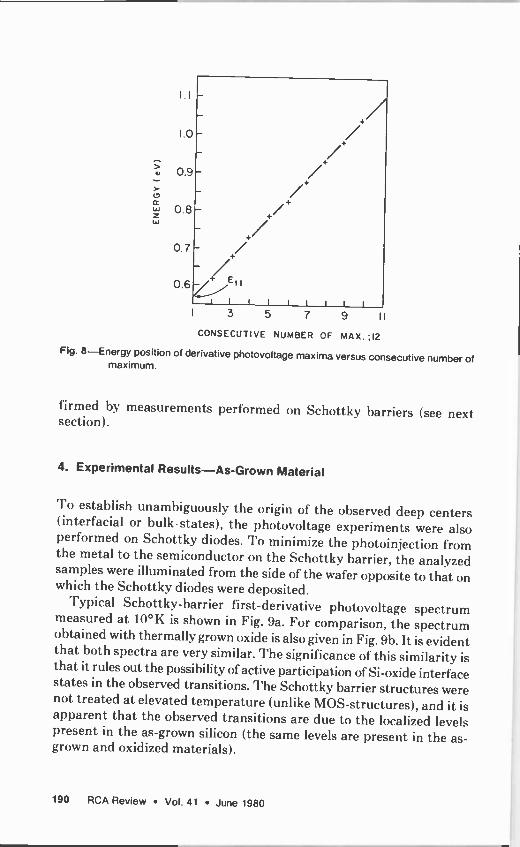
1.0
0.9
0.8
0.7
0.6 I I I
3 5 7 9 II
CONSECUTIVE NUMBER OF MAX. ;12
Fig. 8-Energy position of derivative photovoltage maxima versus consecutive number of maximum.
firmed by measurements performed on Schottky barriers (see next section).
4. Experimental Results-As-Grown Material
To establish unambiguously the origin of the observed deep centers (interfacial or hulk -states), the photovoltage experiments were also performed on Schottky diodes. To minimize the photoinject ion from the metal to the semiconductor on the Schottky barrier, the analyzed samples were illuminated from the side of the wafer opposite to that on which the Schottky diodes were deposited.
Typical Schottky -barrier first -derivative photovoltage spectrum measured at 10°K is shown in Fig. 9a. For comparison, the spectrum obtained with thermally grown oxide is also given in Fig. 9b. It is evident. that both spectra are very similar. The significance of this similarity is that it rules out the possibility of active participation of Si -oxide interface states in the observed transitions. The Schottky barrier structures were not treated at elevated temperature (unlike MOS-structures), and it is apparent that the observed transitions are due to the localized levels present in the as -grown silicon (the same levels are present in the as - grown and oxidized materials).
190 RCA Review Vol. 41 June 1980

PHOTOVOLTAGE SPECTROSCOPY
MS
MOS
1 I I I I t 1
0.5 0.7 0.9 I.I
PHOTON ENERGY (eV)
Fig. 9-First derivative surface phctovoltage spectra of the as -grown sample (MS -structure)
and the MOS structure (oxidized sample).
5. Procedure for Determination of the Deep Level Parameters
For small excitation level the photovoltage, .1V, is proportional to the concentration of generated excess holes, Ap,
.nV = C.Ap. [ 1 1
For the photoionization transitions of Fig. I b, .gyp = .fin, where .5n, is the change in concentration of electrons at levels E,.
At low temperature, the thermal generation transitions are negligible and the rate equation for nt is
dn, X21 =G,-Ku,,
dt where G, is the rate of photoionization transitions from valence band into the levels E,, and R,,, is the rate of recombination transitions from Et to valence band. Thus,
G, = Io;Nt; Rtu = Kpntp, 131
where l is the photon flux, a; is the photoionization cross section, Alt is
the total concentration of deep levels (note that in p -type material at low temperature all deep levels are practically empty, i.e., n, « N,), Kp is the effective capture cross sect ion for holes, and p is the concentration of free holes (p = po + .gyp where po is the hole concentration in the dark).
It follows from Eqs. 111-131 that (a) the steady state photovoltage
Vo = CIcr;N,r, 14a1
where
RCA Review Vol. 41 June 1980 191

1 r= K p p
(b) the photovoltage transient following "illumination on" is
= ..5V0(1 -e-r/T);
(c) the photovoltage transient following "illumination off" is
V = Voe-t/T.
]4b]
]5]
]6]
Eqs. 141-16] provide a simple basis for the determination of deep -level parameters from measured values of r and Vo. As discussed below, the validity of these equations has been verified by experiments performed on MOS structures.
1. It has been found that the amplitude of steady-state photovoltage Vo increases linearly with illumination intensity (see results given
in Fig. 10) in agreement with Eq. ]4a]. Also in agreement with ex- pression 4, -5 Vo was found to increase drastically with decreasing temperature (see Fig. 11). Such photovoltage enhancement at low temperature is due to a decrease of hole concentration Po and thus an increase of the relaxation time r = 1/(Kpp).
2. It has been found that under low intensity suhbandgap illumination (..5p « po), the photovoltage transient is exponential (Eqs. ]5] and
0'
102
10
1010
hu =.80 eV
hu=.9sev
+:
1012 10
PHOTON FLUX (cm 2 1)
/ e' i
0"
Fig. 10-The magnitude of steady-state photovoltage versus photon flux for different photon energies hi,.
192 RCA Review Vol. 41 June 1980

PHOTOVOLTAGE SPECTROSCOPY
4
10
TEMPERATURE (K)
40 30 20 15
i 1 1 1
:+ +
103- ,
i/A e A
A
A
102 ACTIVATION ENERGY
Ea'46±3meV
A
2 3 4 5 6 7 8 9
100 T
Fig. 11-Temperature dependence of steady-state photovoltage generated by photons of by = 0.75 eV. The results for sample S1 and S2 were displaced in a vertical di- rection for clarity. (Identical activation energy was also obtained for inc'dent photon energy corresponding to photoionization of the levels En.)
161). The value of time constant r increases with decreasing temper- ature.
3. It has also been found that at low temperatures (T = 12°K) and for high illumination intensity (I > 1015 photons/cm2 s), the time con- stant r decreases with illumination intensity (i.e., .Sp becomes com- parable to po). This observation is of significance, as it enables a simple estimation of the concentration of deep levels. For example, it was observed for sample S1 at 12°K that background illumination with 2 X 10¹⁵ photons/cm2 s of h i' = 0.75 eV reduced the relaxation time by about 10%. Accordingly, ,.5p was estimated to be about 0. Ipo
108 cm -3. From the value of .Sp and the magnitude of photovoltage V, the scaling factor C in Eq. 111 was evaluated, permitting the further quantitative analysis. In the experimental determination of the relaxation time r, the
chopped light technique was employed, which enabled the use of a high -sensitivity lock -in detection of an ac signal. Thus, if sul,banclgap low -intensity illumination is periodically modulated with a frequency (, the measured amplitude of photovoltage is)s
MVP = .Vo(1 + w2r2)-I/2, 171
RCA Review Vol. 41 June 1980 193

hv=.75eV T=12K / T= 9.5m
0 / -5
/o - 20 10
T=25K
a r5.3ms A-' ,r,'- -12 ó o/ A''" - e - A"á iA = TAN a
B _4
1 f I I I 1 I I
2 4 6 8 10 12 14 x102
f2 (Hz)2
Fig. 12-Frequency dependence of photovoltage generated by periodically modulated il- lumination (hi, = 0.75 eV).
where w = 27f. If (.1V,,)-2 is plotted versus f', a straight line is obtained (see Fig. 12).
Using the notation of Fig. 12, the slope A and the value of B enable the determination of r:
= 1 R r2r
A 181
As shown in Fig. 12, r indeed decreases with temperature, but the product ..Vo/r is practically independent of temperature, in agreement with Eq. 141.
6. Quantitative Results
6.1 Compensation of the Material (Oxidized Samples)
For low illumination intensity the amplitude of steady-state photovol- tage (see Eq. 141) becomes
AVo = CI cr;Nt 1 . 191 KPo Hole concentration Po is the only quantity in Eq. 191 that depends sig-
194 RCA Review Vol. 41 June 1980

PHOTOVOLTAGE SPECTROSCOPY
nificantly on temperature. Accordingly, log( -5V0) versus I/T provides a simple means for determination of the freeze -out characteristics (i.e., -logpo versus 1/T). The results obtained for the samples S1 and S2 are given in Fig. 12. The obtained activation energy is in excellent agreement with the energy level of a shallow acceptor due to the boron EA = 46 meV.16"'
The freeze -out characteristic in the form e_EA, 'V is significant,18 as it indicates that the supplied samples exhibit noticeable compensation (note that for noncompensated material the freeze -out characteristic should be p e-EA/2k'').18 Thus, for the temperature range of Fig. 12,
the concentration of compensating donor centers, ND, in Si samples must satisfy the inequality Ni) » 1/2Ne-EA/kT,18'9 where N is the effective valence band density of states; i.e., N can realistically he estimated as much higher than 1013 cm -3.
6.2 Parameters of Deep Levels
From the measured values of' the relaxation time at photon energy cor- responding to photoionization of the previously reported deep levels, the effective capture cross section has been determined at 7' = 12° K for the samples S1 and S2. For the Si samples, po at 12°K was estimated to he about 109 cm -3. Utilizing this value and the measured time constant, r, the capture cross section for holes was estimated as (p = (rpcu7)-1, where uT = (3hT/m*o) is the thermal velocity of the holes.
The concentration of deep levels N, was estimated from Eq. [41, and the magnitude of' contribution to the photovoltage was provided by a given level (..5 V 1 and J V2 for levels E,1 and E,2, as, for example, in Fig. 7). The required values of photoionization cross sections a; were esti- mated from the quantum defect model (a; = [2.5 X 10⁻¹⁸ cm2I/ Er 2).2"
The obtained dynamic parameters of deep levels are listed in Table 2. It should be mentioned that although the absolute values of these parameters contain uncertainty due to estimation of hole concentration, po and/or the value of photoionization cross section R;, the relative changes of N, between samples S1 and S2 are determined with much better accuracy (about 20%).
Table 2-Deep-Level Parameters
r at 12°K ;ms) aP I,eveq (eV) Sample I Sample 2 (cm) Sample 1 Sample 2
E.,1 0.56 11 9.5 -10-11 2 X 10¹³ 9 X 10¹²
E,2 <0.5 >45 >40 >2 x 10-15 <1012 <5 x I011
RCA Review Vol. 41 June 1980 195

7. Summary
High resolution measurements of the derivative surface photovoltage spectroscopy have revealed the presence of deep and shallow energy levels in the as -grown and oxidized samples of high quality float zone Si. Thus, deep level transitions at energies El 1 = 0.56 eV and Et2 < 0.5 eV were clearly observed at temperatures below 30°K. Higher energy transitions are characterized by strong coupling with phonons, and corresponding energy levels apparently represent the recombination levels. It is also shown that these levels are due to the bulk states rather than interface states.
The transitions to the shallow level (45 meV below energy gap) have been observed for a narrow temperature range, and they have been tentatively identified as valence band-shallow electron trap transi- t ions.
Transient characteristics of the photovoltage were employed to evaluate the concentration and the capture cross section of residual deep levels in high purity Si. It has been found that the concentration of the levels in the oxidized wafers is between 10" and 1013 cm -3 and the capture cross section for holes is 10-14 cm2 or less. From free hole freeze -out characteristics, it has been established that the high purity p -type Si contains shallow compensating donors at a concentration much higher than 1013 cm -3. The concentration of deep and shallow centers has been found to exhibit noticeable variations between the analyzed samples.
References:
C. T. Sah and C. T. Wang, J. Appl. Phys., 46, p. 1767 (1975). 2 P. M. Petroff, D. V. Lang, J. L. Strudel and R. A. Logan, Scanning Electron Microscopy (1978), Vol.
1, p. 325, SEM Inc., AMF O'Hare. 3 L. Jastrzebski, P. Levine, D. Cope, W. Fisher, D. Savoye, and W. Henry, 157th Electrochem. Soc.
Meeting, St. Louis, May 1980 (abstract No. 150) (to be published in J. Electrochem. Soc.). 4 L. Jastrzebski and J. Lagowski, 17th Electrochem. Soc. Meeting, St. Louis, May 1980 (abstract No.
152) (to be published in the J. Electrochem. Soc.). 5 For review, see C. T. Sah, Semiconductor Silicon 1977, H. R. Duff and E. Sirtl, Editors, p. 868, The
Electrochem. Soc. Softbound Symposium Series, Princeton, NJ (1977); G. L. Miller, D. V. Lang and L. C. Kimerling, Ann. Rev. Material Sci., 1977, p. 377; H. G. Grimmeiss, Ann. Rev. Material Sci.. 1977, p. 341.
6 H. M. DeAngelis, J. W. Diebold and L. C. Kimerling, Radiation Damage and Defects in Semiconductors, London Institute of Physics, 1973, p. 295.
See e.g., J. A. Pals, Solid State Electron, 17, p. 1139 (1974). 6 See e.g., O. Engstrom and H. G. Grimmeiss, J. Appl. Phys., 47, p. 4030 (1976). 9 J. Lagowski, W. Walukiewicz, M. M. G. Slusarczuk, and H. C. Gatos, J. Appl. Phys., 50, p. 5059
(1979).
10 E. Kamienicki, J. Lagowski, and H. C. Gatos, J. App!. Phys. (1980) (in press). " J. Lagowski, Proc. of 3rd Univ./Industry/Government Microelectronic Symp., Lubbock, Texas, 1979, IEEE Conf. Record, p. 1.
12 L. Jastrzebski, P. Levine, D. Cope, W. Kosnocky, W. Henry, and D. Batson (submitted to IEEE Pro- ceedings).
196 RCA Review Vol. 41 June 1980

PHOTOVOLTAGE SPECTROSCOPY
t3 See, for example, Handbook of Electronic Materials, ed. M. Neuberger, IFI/Plenum, New York, 1971,
Vol. 5.
1a K. L. Shaklee and R. E. Nahory, Phys. Rev. Lett., 28, p. 942 (1970). 15 S. M. Ryvkin, Photoelectric Effects in Semiconductors, New York Consultants Bureau, 1964, ch.
III.
16 J. P. Maitz, Phys. Rev., 96, p. 28 (1954); F. J. Morin, et al., Phys. Rev., 96, p. 833 (1954).
17 E. Burstein, et al., J. Phys. Chem.. 57, p. 849 (1953).
18 See, for example, R. A. Smith, Semiconductors, Cambridge University Press (1959¡. Ch. 4, 3, p.
82-92. 19 5. M. Sze, Physics of Semiconductor Devices, John Wiley 8 Sons, New York, 1969. p. 35.
20 See, for example, P. R. Bratt in Semiconductors and Semimetals, ed. R. K. Willardson and A. C. Beer,
Academic Press, New York, 1977, Vol. 12, Ch. 12, and references quoted therein.
21 From the measurement of diffusion length done by surface photovoltage. e.g., Annual Book of ASTM Standards (ASTM, Philadelphia, 1974), p. 752.
RCA Review Vol. 41 June 1980 197

GaAs MESFET Comparators for Gigabit -Rate Analog -to -Digital Converters
L. C. Upadhyayula
RCA Laboratories, Princeton, NJ 08540
Abstract-A novel MESFET comparator circuit has been proposed. A three -comparator circuit has been fabricated with discrete GaAs FETs and evaluated up to 250 -MHz clock rates. The comparators and coding logic for a 2 -bit A/D converter have also been designed. The performance of the converter has been studied using a computer simulation program. The simulations indicate that the circuit will function satisfactorily up to 1.0 GHz sampling rates. The development of a monolithic IC chip consisting of comparators and coding logic is also reported.
Introduction
Multigigabit-rate signal and data processing is required for government as well as commercial systems of the mid -to -late 1980s. Ana og-to-digital converters are an essential part of such signal processing circuits. McCabe' and Griffiths2 have reported that three- to four -bit A/I) working at 1-2 GHz sampling rates will satisfy the needs of many future systems. The fastest silicon bipolar -technology based A/D is a 5 -bit A/D operating at 400 MS/s reported by DeGraafe.3 It is believed that, due to excessive power dissipation, this technology cannot be advanced to higher sampling rates. In the past four or five years, GaAs -based tech- nology has emerged as a candidate for high-speed signal processing. I). C. Claxton, et al.,4 attempted to develop a 1 -bit A/I) cell using a combi- nation of GaAs transferred -electron logic devices (TEI,I)s) and field- effect transistors. This work was plagued by the poor performance of the TELDs, their bias instabilities, and low gain in the MESFETs. New
198 RCA Review Vol. 41 June 1980

GaAs MESFET COMPARATORS
circuit approaches and/or novel applications of the state of the art de- vices are necessary to meet the gigabit -rate A/D requirement.
An excellent review on analog -to -digital converters (ADC) was given by Gordon, et al.5 A parallel comparator ADC, which represents the architecture with the highest speed and a reasonable accuracy, is sche- matically shown in Fig. 1. The critical components in an ADC are (1) sample and hold circuits, (2) amplifiers, (3) threshold comparators, and (4) latches and decoder logic circuits. The speed of an AI)C is determined by the speeds of the individual components. Operating at room tem- perature ambient, GaAs MESFETs demonstrated 32-60 ps propagation delays5'7 and power amplification up to 37 GHz.8 These properties have been utilized in developing high-speed sample and hold circuits,9 am- plifiers,10 and digital logic circuits.' 1,12
GaAs MESFET comparators operating at 1-2 GHz rates were first proposed by the author recently ':t and are the subject of this paper. We concern ourselves with the design, fabrication, and evaluation of these comparators. A novel F1.71' comparator circuit is described. Experimental results on an MIC three -comparator circuit with discrete GaAs FETs are reported. The design of a monolithic comparator for a 2 -bit A/D is
discussed and the results of a computer simulation of its performance are presented. The development of a monolithic integrated circuit chip consisting of comparators and coding logic are also reported.
Principles of Operation of MESFET Comparators
A comparator circuit is one that is used to mark the instant when an input signal with an arbitrary waveform attains some reference or threshold level, at which point the comparator output changes abruptly from its quiescent value. A block diagram of the comparator and its output waveform are shown Fig. 2. The output remains at quiescent value for input signal levels below the reference or threshold level. The
HOST
SIC.
BIT
LEAST
SIG. BIT
LATCHES
DIGITAL OUTPUT
Fig. 1-Schematic of a parallel comparator analog -to -digital converter.
RCA Review Vol. 41 June 1980 199

INPUT COMPARATOR OUTPUT
(o)
VH
INPUT VOLTAGE
(b)
Fig. 2-A block diagram of a comparator and its transfer characteristics.
threshold voltage (Vo,) can be varied by varying the circuit parameters or operating point. The slope of the output is determined by the gain in the comparator circuit. The device to which the comparator output is applied will respond when the comparator output rises to some level. As a consequence, there is variability V; in the precise moment at which the device responds and an uncertainty in time corresponding to this. .IV; should be small compared to the threshold voltage (lit,, ).
An FET comparator circuit is shown in Fig. 3. This circuit looks similar to a single -input inverter used in digital circuits, but the similarity ends right t here. The device and material requirements are totally different from that for the digital circuits. The comparator circuit consists of a
Fig. 3-FET Comparator.
VDD
LOAD
r -
INPUT
SWITCH SECTION
SOURCE
FOLLOWER
LEVEL SHIF" DIODES
OUTPUT
CURRENT
SOURCE
V55
200 RCA Review Vol. 41 June 1980

GaAs MESFET COMPARATORS
switch transistor (Ts). a load transistor (T),), and a level shifting circuit that makes the output pulses compatible with the input requirements of the following digital circuit. The drain saturation current for the switching transistor is higher than that for the load transistor. A nega-
tive -going input pulse at the switch transistor gate electrode makes it less conducting, allowing the internal node voltage to rise. As the input pulse varies from 0 volts to about -1.2 volts, the node voltage rises from +0.5 volts to +4.0 volts. The level shifting circuit translates this to an output whose amplitude and dc level are compatible with the input pulse required for driving digital logic circuits.
The response (rise) time and the threshold level of the comparator are determined as follows. The critical node in this comparator circuit is the drain of the switch transistor. The rise and fall times of the output pulse are determined by the charging and discharging of the load ca-
pacitance present at this node. The switch and load transistors along with
the capacitive load is shown in Fig. 4a. The current voltage characteristic of the switch transistor with the load line superimposed is shown in Fig.
4b. When the input to the gate of the switch transistor is 0.0 V, the out put stays at VL which is of the order of 0.5 V. Application of a negative signal at the gate of TS decreases its drain current and changes the point of intersection for the load line. However, the voltage at the output node does not change appreciably until the drain current of the switching transistor is equal to that of the load transistor. When the input voltage becomes more negative, the operating point shifts to Vrr. The capaci- tance load presented at the drain must be charged before this voltage transition occurs. The rate at which the drain voltage changes is given by
JV 1 C' I11
where :51 is the current available for charging, C is the load capacitance,
YOLTICE
b ) 111
Fig. 4-Current-voltage characteristic of the threshold circuit for comparator operation.
RCA Review Vol. 41 June 1980 201

V is the voltage transition and ,1 is the switching (rise) time. For a typical circuit, C 0.02 pF and V ^ 3.0 V. Hence, a 0.6-mA current change will he required to make the transition in 100 ps. The rise time is thus dependent upon the current drive capability.
The switching transition takes place when the drain current of the switch transistor (Ts) is equal to that of the load transistor (Ti,). This is achieved by the application of an input signal VG at the gate of Ts. The condition for the drain currents of Ts and TL to be equal is given by:
Ins L(I
- 1 =-= K
I nr, (1 - where
121
11s = Vf/VP, 1 = (VG + WV P9
Vii = built-in Schottky harrier voltage;
Vp = channel pinch -off voltage;
K = width of the switch transistor/width of the load tran- sistor.
For Schottky barriers on GaAs, VII is of the order of 0.4 to 0.6 V. For a given channel pinch -off voltage and desired threshold voltage (VG = Vo,), the design parameter K is evaluated from Eq. 121. The design of a three -comparator circuit for a 2 -bit A/D will be discussed later.
Experimental Results on an MIC Comparator with Discrete MESFETs
The principle of FET comparators is demonstrated using the three -
lo)
Fig. 5-A three -comparator circuit.
(I)
202 RCA Review Vol. 41 June 1980

GaAs MESFET COMPARATORS
comparator circuit shown in Fig. 5. This circuit was fabricated in MIC form using discrete GaAs power FETs. Each of the FETs has four gate stripes and each stripe is 150 pm wide. The four gates of each switch transistor (T81, Ts2, and TS3) are connected in parallel resulting in a total gate width for each of 600 pm. For the load transistors T1,1i Tt,2, and Ti.t, we have used three, two, and one gate stripes, respectively. These tran- sistors were mounted in an MIC circuit to provide 50 ohm connections for the input and output signals. The input pulse was provided from an HP 214 or 8091 pulser.
The output was measured on a sampling oscilloscope with and without high impedance probes. The high impedance probe was used to minimize the capacitive loading. The performance of the comparators for do or low frequency input signals is shown in Fig. 6. Note the three distinct threshold levels for the three comparators. The performance on the comparator circuit for a 250 MHz input signal is shown in Fig. 7. The operation of this circuit was very satisfactory. In our experiments, the output was measured at the comparators with a sampling oscilloscope fitted with high impedance probes. No output driver or source follower stages were used. In general, the output driver greatly enhances the circuit's ability to drive a bigger (capacitive) load of other circuits with a minimal increase in propagation delay.
3.0
2.5
OUTPUT OZ
2.0 - OUTPUT 0,
OUTPUT
VOLTAGE
(VOLTS) 1.5
1.0
0.5
OUTPUT C;
0.5 1.0 1.5 2.0 25 3.0 3.5
INPUT VOLTAGE (VOLTS)
Fig. 6-Performance of a GaAs three comparator circuit; discrete FETs were used in an MIC circuit.
RCA Review Vol. 41 June 1980 203

0.5V/ DIV
0.5V/DIV
0.5V/DIV
t 1 .
Fig. 7-Response of the three -comparator circuit to 250 MHz input signal.
Monolithic A/D Design
A two -hit A/D is shown schematically in Fig. 8. It has three comparators and binary coding logic. The comparators are the FE I' comparators discussed earlier and the logic gates are the standard depletion mode NAND/NOR gates. A circuit diagram of the two-bit A/D including the comparators and coding logic is shown in Fig. 9. The comparator threshold voltages have been set to 0.4, 0.8, and 1.2 V. The parameter 1/K (i.e., ratio of the widths of the load and switch transistors) has been calculated for these three threshold voltages from Eq. 121 and the results are presented in Table 1. A channel pinch -off voltage Vp = 5 V is as -
204 RCA Review Vol. 41 June 1980

GaAs MESFET COMPARATORS
INPUT
Fig. 8-Block diagram of a parallel threshold A/D converter.
2'
PARALLEL OUTPUTS
2
sumed and a Schottky harrier built-in potential of 0.4 and 0.6 V is used.
From Table 1 it is clear that the parameter 1/K is not very sensitive to the variation of Schottky harrier potential. Furthermore, photolitho- graphic techniques allow geometry control to within a micrometer. Therefore, these comparators are realizable in practice. This design
procedure gives us the ratio of the widths of the load and switch FETs only. The actual widths have to be determined from the overdrive voltage required to make the transition at the threshold level.
The overdrive voltage (.A Vg) required for FET comparators is deter- mined as follows. The comparator outputs have to drive the logic gates
used for binary coded conversion. These logic gates will respond as soon
as the comparator voltage has reached a certain level. At the threshold value, the transition from LOW to HIGH or HIGH to LOW takes place
with a small change in input gate voltage (-1 Vg). This value of the gate
voltage should be very small compared to the least significant bit (LSf3) for A/I). As discussed before, the load and the switching transistors of the comparator provide the charging or discharging currents, respec-
tively, for the capacitive load. The load on the comparator is the input capacitance of the source follower and is of the order of 0.02 pF. There- fore, the current required for charging or discharging is
.5/ = C V . 131
Table 1-Comparator Design Parameters for 2 -Bit A/D.
Comparator Threshold
Built -In Voltage
Width of the Load FET/Width of the Switch FE'I'
L'P=5\ Vr,=6V
0.4 \ 0.6 V 0.845 0.865 0.8 0.720 0.756 1.2 0.612 0.661
0.4 0.4 V 0.837 0.856 0.8 0.711 0.745 1.2 0.606 0.652
RCA Review Vol. 41 June 1980 205

2I output
Input
20 output
Fig. 9-Circuit diagram of the two-bit A/D.
The voltage change at the comparator output is of the order of 3 V. For the switching transition to occur in 100 ps, a current change of 0.6 mA is needed. The change in FET current is caused by a voltage change (Vg) at the gate and is given by:
= g, .1 Vg, 141
where g, is the transconductance. An FET with 6-mS transconductance will bring the 0.6-mA current change for ,Vg = 0.1 V.
The minimum size of the FET was determined from the graphical design procedures described by K. B. Fair.14 The optimum doping density for FETs is 8 - 10 X 1016cm-3. The minimum gate length pos- sible with optical lithography and contact printing is 1.0 pm. The drain saturation current (//)ss) and transconductance as computed from Figs. 4 and 6ofFairi4 are mss= 17.5-' ?0mA and g,,, = 7.0 - 7.5 mS for a 10(1
206 RCA Review Vol. 41 June 1980

GaAs MESFET COMPARATORS
pm wide device with 5-6 V channel pinch -off voltage. The widths of the load transistors are then obtained from the 1/K values given in Table 1. The driver/level shifting circuits and the NAND/NOR gates were designed using standard techniques.
Fig. 10 shows the layout of the 2 -hit A/I). The total power dissipation for the proposed all -parallel 2 -bit A/D converter using GaAs FETs is
about 400 mW. This corresponds to about 200 mW per bit, which is
substantially lower than that for silicon bipolar -based A/D circuits. Sensitivity of the circuit to process variations can be a problem. The
device parameters that vary during processing and that we generally come across in GaAs MESFE'I's are (a) Schottky harrier built-in voltage (VB) and (h) the pinch -off koltage (VP). The variation in VP occurs due to changes in doping density and channel thickness. It was pointed out earlier that variations in VB do not effect the step size (see Table 1) and,
GND J
[-1
11
-vis
1lll 11LW ULll J l. ij 111111 II 1L111 U11ll ü1.
GND
Fig. 10-Layout of the 2 -bit A/D.
INPUT
RCA Review Vol. 41 June 1980 207

Table 2-Effect of Pinch -off Voltage on Comparator Threshold Voltage.
Threshold Voltage (Vth )(Volts) I/K Vp=6.0V Vp=5.0V VI = 4.0 V
0.845 0.170 0.40 0.32 0.720 0.946 0.80 0.649 0.612 1.129 1.20 0.963
therefore, the comparator performance. The step size does vary with changes in pinch -off voltage, however. The variation of step size for a ±20% variation in pinch -off voltage is shown in Table 2.
A pinch -off voltage of 5 V, a step size of 0.4 V, and Schottky built-in voltage of 0.6 V were used in these calculations. From the table, ít is clear that the linearity is maintained even though the step size is changed. Because the change in the step size is linear, it can easily be accounted for by adjusting the gain of the amplifier in front of the comparators (see Fig. 1).
Computer Simulation of the 2 -Bit A/D
Before fabricating the IC chip, the performance of the comparator and level shifting circuits was studied using a computer program with a user -defined model for the GaAs FET. This user -defined model requires measured device parameters, and the /- V characteristics of the discrete power FETs were used to obtain these parameters. The output of the three comparators and level shifting circuits was monitored as a function of input signal voltage. Threshold characteristics and response time are the two important parameters of interest. A slowly varying input signal was used to determine the threshold characteristics. The comparator response as a function of input voltage is shown in Fig. 11 for threshold voltages of 0.4, 0.8, and 1.2 V. The comparator output changes from LOW to H IG H for an input voltage change of 0.1 V around the threshold val- ues. These results are in good agreement with the design goals. The actual output levels are 1.0 V for LOW and 5.0 V for HIGH. These voltage levels have to be brought hack to logic levels using level shifting circuits. The level shifted output of the comparators is shown in Fig. 12. In the absence of an input signal, the level shifted outputs are -2.5 to -3.0 V and cor- respond to logic "0". When the input signal reaches the threshold value, the level shifted outputs reach 0 to +0.5 V corresponding to logic "1". It appears that the transition from LOW to HIGH of the level shifted outputs is much sharper than the comparator outputs themselves.
In the final application, a sample -and -hold signal will feed the com- parators. The level shifted comparator outputs are therefore studied with sample -and -hold type input signals. A sample t ime of 100 ps and a hold
208 RCA Review Vol. 41 June 1980

GaAs MESFET COMPARATORS
6.0
5.0
4.0
3.0
2.0
1.0
-0.2 -0.4 -0.6 -0.8
INPUT (V) -1.0 -1.2
Fig. 11-Computer simulation of the comparator response for 2 -bit A/D.
time of 400 ps were used for these simulations. The response of one of the comparators is plotted in Fig. 13. From this plot, the comparator response time seems to he about 300 400 Ps.
These computer simulations indicate that the comparator and level shifting circuits work very satisfactorily at above 1.0 GHz sampling rates.
INPUT (V)
Fig. 12-Computer simulation of the comparator and level shifting circuits for 2 -bit A/D.
RCA Review Vol. 41 June 1980 209

Fabrication of Monolithic A/D Circuits
A tentative process schedule was developed for the IC fabrication. Eight masking steps are necessary to complete the IC. Au:Ge/Ni alloyed ohmic contacts are used for source and drain. Ti/Pd/Au metal system is used for Schottky harrier gates and interconnections. The IC fabrication has been completed. Fig. 14 shows a photomicrograph of a fabricated chip. Test circuits are being evaluated now and the IC will he evaluated soon.
Conclusions
A novel GaAs MESFET circuit has been proposed for high-speed com- parator applications. The operation of such comparators has been suc- cessfully demonstrated experimentally up to 250 MHz clock frequencies using a hybrid MIC circuit with discrete MESFETs. Comparators and binary coded logic circuits have been designed for a 2 -bit A/D. Computer simulations of this circuit indicate that it will function satisfactorily above one GHz sampling rate. A GaAs monolithic IC chip consisting of the comparators and coding logic is being developed. The availability of these comparators will make it possible to develop a single chip GaAs MESFET A/D working at a gigabit sampling rate.
0.5
--0.2
-05- - %I%\ --0.4
:.:: :::: = i ~-
-2.0 --I.0
-2.5- -1.2
3.0 I I I -1.4 0 200 400 600 600
TIME (p+)
Fig. 13-Computer simulation of input.
1000
the response of LSB comparator for sample -and -hold
210 RCA Review Vol. 41 June 1980

GaAs MESFET COMPARATORS
-
rI 1 (I
. L.' '
Fig. 14-Photomicrograph of a 2 -bit A/D chip fabricated.
Acknowledgment
The author would like to thank I)r. W. H. Curt ice for providing the model of the GaAs FET used in the computer simulations. The author is also indebted to I)r. S. Y. Narayan and I)r. F. Sterzer for many stimulating discussions.
References:
Robert McCabe, Panel discussion at Workshop on High -Speed A/D Conversion, Portland, OR, Oct. 1978.
2 Lloyd J. Griffiths, "Hybrid Adaptive Array Processing Using A/D Converters," Digest of papers. First Specialty Conference on Gigabit Logic for Microwave Systems, Orlando, FL, pp. 51-52, May 1979.
3 K. DeGraafe, "A Silicon 400 MS/s 5 -Bit A/D Converter," Workshop on High -Speed A/D Conversion, Portland, OR, Oct. 1978.
" D. L. Claxton, et al., "TED IC Technique Evaluation and A/D Cell Development," ONR Final Rept., Contract No. N00014 -76-C-0743, TRW Defense and Space Systems Group, Redondo Beach, CA, February 1978.
B. M. Gordon, "Linear Electronic Analog/Digital Conversion Architectures, Their Origins, Parameters, Limitations and Applications," IEEE Trans. Circuits and Systems, p. 391, July 1978.
6 R. L. VanTuyl and C. A. Leichti, "High -Speed Integrated Logic with GaAs MESFETs," ISSCC Digest of Tech. Papers, p. 20 Feb. 1974.
r P. T. Greiling, C. F. Krum, F. S. Ozdemir, L. H. Hacket, and R. F. Lohr, Jr., "Electron -Beam Fabricated GaAs FET Inverter," 36th Annual Device Research Conf., June 1978, Univ. of Cal, Santa Barbara, CA.
8 J. M. Schellenberg, et al., "RF Characteristics of Ku -Band FETs," Seventh Biennial Conf. on Active Microwave Semiconductor Devices and Circuits, Aug. 1979, Cornell Univ., Ithaca, NY.
RCA Review Vol. 41 June 1980 211

9 P. H. Saul, "A GaAs MESFET Sample and Hold Switch," to be presented at the 1979 European Solid State Circuits Cont., 1979. 10 R. L. VanTuyl, "A Monolithic Integrated 4 GHz Amplifier," ISSCC Digest of Tech. Papers, p. 72, Feb. 1978.
11R. L. VanTuyl and C. A. Leichti, "High -Speed GaAs MSI," ISSCC Digest of Technical Papers, p. 20, Feb. 1976. 12 R. C. Eden, et al., "Low Power GaAs Digital ICs Using Schottky Diode FET Logic," ISSCC Digest of Technical Papers, p. 68 Feb. 1978. 13 L. C. Upadhyayula," GaAs FET Comparators for high-speed Analog -to -Digital Conversion," Digest of Technical Papers, GaAs IC Symposium, Lake Tahoe, Nevada. Sept. 1979. 14 R. B. Fair, "Graphical Design and Iterative Analysis of the DC Parameters of GaAs FETs," IEEE Trans. Electron Dev., Ed -21(6), 357, June 1974.
212 RCA Review Vol. 41 June 1980

Comparison of Phase -Only and Conventional Monopulse in Thermal Noise
Carmen N. Campopiano
RCA Missile and Surface Radar Div., Moorestown, NJ 08057
Raymond S. Berkowitz
Moore School of Electrical Engineering, University of Pennsylvania, Philadelphia, PA
Abstract-This paper compares the noise immunity of two monopulse algorithms-a form
of conventional monopulse and a phase -only algorithm. Specifically, we treat pulse compression systems with pseudorandom coding in additive thermal noise. It is shown that, in the absence of limiting, the two algorithms have essentially identical performance, prcvided the ratio of energy over noise power density (E/No) is at least 14 dB, and that the target offset from the null is small. Witn hard i -f limiting, the conventional monopulse algorithm treated here cannot operate, while
the phase -only algorithm suffers a loss relative to linear operation of 2 dB or less.
1. Introduction
In this paper, we compare the angle estimation performance of a form of conventional monopulse with a phase -only algorithm in thermal noise. The phase -only algorithm is useful in that it can still perform well with amplitude limiting. On the other hand, it is important to compare the phase -only system with conventional monopulse in order to determine how much one gives up for this compatibility with limiting. This com- parison is made here. Both analytic and Monte Carlo results are given. To he concrete, we use both algorithms in a system with pseudorandom coded waveforms and pulse compression.
RCA Review Vol. 41 June 1980 213

The presentation is organized as follows. The two monopulse algo- rithms are defined in Sec. 2. Models for the performance of these algo- rithms in thermal noise are given in Sec. 3, and the models are analyzed in Sec. 4. Both Monte Carlo and approximate analytical results are presented in Sec. 5. Conclusions appear in Sec. 6.
2. Definition of the Monopulse Algorithms
Before developing a model of the signal processing and thermal noise effects (see Sec. 3), we define the two monopulse algorithms under dis- cussion. We suppose that an antenna, e.g., an array, supplies the re- ceiver/signal processor with two phasor inputs
(t) = e,,,P(t)g(tl)eio = sum beam phasor
(t) = e,,,P(t )h (ll)elo = difference beam phasor, ¡1l
where
g(0)= sum beam pattern
h(0)= difference beam pattern
11 = target offset from monopulse null (normally one of two angle coordinates)
= phase of received waveform relative to local reference
P(t) = ±1 = pseudorandum modulating waveform
em = received peak signal amplitude.
For simplicity we treat only one angle coordinate. In the absence of noise and instrumentation errors we would have
1; h(n> = 11= f(0) 121
where p is the monopulse error ratio. The relation p = f(0) is deter- mined by the antenna. The function of a monopulse algorithm is to es- timate p.
Let us define the monopulse algorithms to he considered here. Let and.. represent the sum and difference signals that result after 2 ; and
are contaminated by additive noise and the resulting noisy waveforms are subjected to pulse compression. By conventional monopulse, we mean a process that estimates p by evaluating
RePI=lm(
214 RCA Review Vol. 41 June 1980
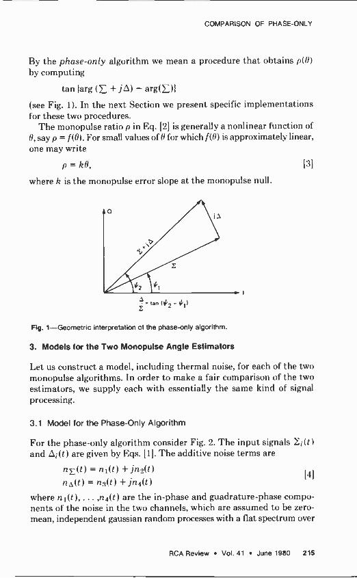
COMPARISON OF PHASE -ONLY
By the phase -only algorithm we mean a procedure that obtains p(tt) by computing
tan {arg ( + j-) - arg(131
(see Fig. 1). In the next Section we present specific implementations for these two procedures.
The monopulse ratio p in Eq. 121 is generally a nonlinear function of H, say p = [(01. For small values of 0 for which ((h) is approximately linear, one may write
p = kt), 131
where k is the monopulse error slope at the monopulse null.
c= tan l4'2-tL11
Fig. 1-Geometric interpretation cf the phase -only algorithm.
3. Models for the Two Monopulse Angle Estimators
Let us construct a model, including thermal noise, for each of the two monopulse algorithms. In order to make a fair comparison of the two estimators, we supply each with essentially the same kind of signal processing.
3.1 Model for the Phase -Only Algorithm
For the phase -only algorithm consider Fig. 2. The input signals !; (t and ,..51(t ) are given by Eqs. 1 l 1. The additive noise terms are
nL(t) = n1(t) + jn2(t ) n,(1) = n3(t) + jn4(t )
where n 1(1), ... ,n4(t) are the in -phase and guadrature-phase compo- nents of the noise in the two channels, which are assumed to be zero - mean, independent gaussian random processes with a flat spectrum over
141
RCA Review Vol. 41 June 1983 215

D 121
c. y,=T.+nú
_I
+ I IF LIM.
IF LIM
PHASE DETECT
VC - PHASE DETECT
Iz
(] CORRELATION DETECTION
IC -.a °C . CORRELATION
DETECTION
._y T
Q
CI
CQ
n MONO- P PULSE P EST.
0 0 0 0 0 Fig. 2-Model for phase -only algorithm.
the signal band and with rms value rr,2.* The input signals 2;; and are modified by additive noise to give signals
E = E¡ + = e2P(t)g(11)eio+ n1(t) +jn2(t) 151 = + n emP(t)h(ll)e&4' + n;;(t! + jn4(t).
Then the signals at point I of Fig. 2 are r and r + j where 2 and are defined by Eqs. (51.
In the present analysis, we suppose that the signals are within the linear portion of the limiters (see Sec. 5.3) so that
uZ=E vc=E+j,.
At point 3 of Fig. 2, we have
= Re(v ); QN- _ /2 (v1,) /, = Re(v ); Qc = in2(uc).
The correlation detector outputs at point 4 are then l = ST P(t)1Z(t)dt _ r ¡=1
N E11 = P(t)((t)dt _ r E
N C/ = J
T P(t)1e(t )dt _ r E
0 Pi/C¡
¡=1
T
CQ=P(t)Qc(t)dt_rEPj(t)c¡,N=TIT. f o ¡=1
(61
(71
181
Here T is the expanded pulse duration, r is the compressed suhpulse We denote the standard deviation of x by ax.
216 RCA Review Vol. 41 June 1980

COMPARISON OF PHASE -ONLY
duration, and N is the code length. We assume that range has been ac-
curately estimated so that the P(t) in Eqs. [8] is in synchronism with the P(t) in Eqs. [1].
Finally, the monopulse ratio p = ((H) is estimated by bp,
bp = tan itan-t (mil
- tan -1 11.-11 Cr
_CQE1-CIEQ
Here subscript p denotes the phase -only algorithm.
3.2 Model for the Conventional Monopulse Algorithm
191
For the conventional monopulse algorithm consider Fig. 3.* The inputs are given by Eqs. [l ] while the noise terms are given by Eqs. [4]. The noise -corrupted inputs (signals at point 2 of Fig. 3) are given by Eqs. 151.
At point 3 of the figure, I i Qz are as in Eqs. [71, while
= Re(s), (d.5 = 1101
The outputs of the correlation detectors, point 4, are N
E,, = f Tl'(t)lElt)dt = r E l';1; o ;=1
EQ = 5 l'(t )((t )dt - r E, P;(; ;=t
-11 = ST
l'(t)i,(f)dt - r ,=1
N -5Q = fT P(t )Q )dt = T E l'rQ.1t
o ;=1
PHASE DETECTOR
PHASE DETECTOR
iz
a z,
CORRELATION DETECTOR Q
Q CORRELATION DETECTOR Q
MONO - PULSE EST.
A
f I 1
0 0 O 0 O O Fig. 3-Model for conventional monopulse.
' For notational consistency .s is rotated 90° In Fig. 3.
RCA Review vol. 41 June 1980 217

where we use the same notations and assumptions as in Sec. 3.1. The conventional monopulse estimator Ic of the monopulse ratio p
is then
¡lc=lm -IQ /I/ + l ,k :i + 1.1,
4. Analysis of Angle Estimation Errors
[12[
I this section, we derive convenient expressions for ¡'n and be, the angle estimators for phase -only and conventional monopulse algorithms, re- spectively.
4.1 Analysis of f)
We define,
ge = emg(0) he = e,nh (()) = pge.
Then from Eqs. [4[ through [71,
I =P;,je coso +nl; QE; = Pige sine, + n2i
IC; = Pi(ge cos(1) - he sln0) + nli - n4i Qci = Pi(ge Sino + he coso) + n2i + n,;;.
1131
1141
Substituting Eqs. [14[ into Eqs. 181 we obtain
rd/T= Ng, cow, +ZI
>,Q/T = Nge sincj, + Z2
= N(ge coscp - he sink) + Z5 [ 151
CQ/T = N(ge sine + he cosh) + Z6.
Since the ni's are independent, zero -mean, normally distributed ran- dom variables with variance a2, the Z1 in Eqs. [ 15[ are also normally distributed with zero mean. In fact, we have
N ZI = Pin li
i=l N
L2 = Z Pin2i
218 RCA Review Vol. 41 June 1980

COMPARISON OF PHASE -ONLY
N Z5= Pi(nli-n4i)
i=
``N Z6 = L Pi(n2i + n3i),
i=1
from which it readily follows that Var(Z1) = Var(Z2) = N Var(Z5) = Var(Z6) = 2N al Cov(Z1, Z2) = Cov(Z5, Z6) = Cov(Z1, Z6) = Cov(Z2, Z5) = 0
Cov(Z1, Z5) = Cov(Z2, Z6) = N 1161
For convenience we introduce the random variables
so that
W 1 = Z 1 Cosa + Z2 since
w2 = -Z1 sint + Z2 cos
W5 = Z5 coso + Z6 since
w6 = -Z5 since + Z6 cosh,
Z1 = w] COW - w2 S111th
Z2 = U)1 sine + u'2 cosa
Z5 = w5 cosa - W6 since
Z6 = W5 sing) + w6 cosO.
Then the w's are zero -mean gaussian random variables satisfying
Var(w1) = Var(w2) = Na;n2 Var(w5) = Var(w6) = 2N471.
Cov(w1, w2) = Cov(w5, w6) = 0
Cov(wl, u'5) = Cov(w2, w6) = Na-2
Cov(wl, w6) = Cov(w2, u'5) = O.
1171
1181
1191
Combining Eqs. 1191, 1151 and 1181, we get
N2geh + Nge(w6 - w2) + Nllew] + wlw6 - w2w5 P
N2g1 + Nge(wl + u'5) + Nhew2 + wlw5 + w2w6 1101
Eq. 1201, with minor modifications (see Eq. 126]) supplies the basis for a Monte Carlo analysis of error in bp. For an analytical approximation to the error in bp we proceed as follows. We assume that
a «N2g1, 1211
RCA Review Vol. 41 June 1980 219

which implies that
In il, I11'2I, I«'5I, 1176I «Nge. [22[
Then, dividing numerator and denominator of Eq. 1201 by N2g1 and linearizing the result, we obtain
pp _ p + - [11 6 - U'2 - pins - p2w2[. I231 Nge
It follows that for Eqs. [21), 1221 we have
C(ñp) = p
Var(p1,) _ (1 [24[
2
No
where 6(X) denotes the expected value of X and 2
E = Nger - received energy
No = Q1,r = one-sided noise power density. Note that for the purposes of a Monte Carlo analysis, it is useful to re- write Eq. [201 as
2Rp + \/2R(X6 - X2)+ 2RpX l + X 1X6 - X2X5 Pp
2R + /2R (X + X5) + /2R1x2 + X1X5 + X2X6 1261
where X; = tv;/(\(r) (i = 1, 2, 3, 4), R = E/No, and
Var(X l) = Var(X2) = 1
Var(X5) = Var(X6) = 2
Cov(Xl, X5) = Cov(X2, X6) = I
Cov(X i, X2) = Cov(X 1, X6) = Cov(X2, X5) = 0.
I25I
4.2 Analysis of 1. c
We present an abbreviated discussion, since the development parallels Sec. 4.1. From Eqs. I 1 I, [4I, and 1101 we obtain I.; and (fir; as in EEgs. 1141, as well as
1.5; = -e,ali(IO)I'; sine - ny
h.5; = e,n,h(ll)P; cos0 + n3;.
These equations imply (using Eqs. I11])
= Ng, cowl) +Zi
220 RCA Review Vol. 41 June 1980

COMPARISON OF PHASE -ONLY
= Nge situp + Z2
-11/r = -Nhe shut, - Z4
= Nhe coso + 7,3,
where N
7,i = P;rtj j = 1, 2, 3, 4. i=t
Then the Zj are independent, zero -mean, normally distributed with
Var(Zi) = j = 1,2,3,4.
Using the transformations in Eqs. 1171 and 18), with the replace- ments
15~í:i Z6` -.Z4,
we get N2hege+Nhew, +Ngew3+w1w3+u.2W4
27 N2gé+2Ngew1+w?+w2 I
J
In Eq. 1271, w1, w2, w3, w4 are independent, zero -mean, normal random variables with variances
Var(w;)=N.r1,i = 1,2,3,4. 128)
Eq. 1271 may be put into the form
2Rp + 2RpX 1 + N/2RX3 + X1X3 + X2X4 - 2R 1- 2 \/2R X 1 + X ¡ + X2
1291
where R =E/N° and X; = w1/(s/Ñ?,1) (i = 1, 2, 3, 4), as before. The Xi
are independent, zero -mean, normal random variables with unity vari- ance. Eq. 1291 is in a useful form for Monte Carlo.
For high signal-to-noise ratio, i.e., for 1 Xi I < 2R , we may linearize Eq. 1291 to get
lc = P+ P X 1 + X3 2pX
á/2R \/2R \/2R Hence, we have for this case,
p
Var(1c) _ (1 + p2)
2/t
Note that from Eqs. 1311 and 12411 we have
Var(%'c) 1 < 1 I F » 11.
Var(j,p) I + p2 No
)30)
1311
1321
RCA Review Vol. 41 June 1980 221

In particular, for high E/No and for p = 0, we have Var(%p) = Var(jic).
5. Numerical Results
Some numerical results that are independent of monopulse slope are given in Table 1. In addition, in this section, we present data in terms of angle errors for a typical narrow beam antenna. The results of Sections 5.1 and 5.2 assume no i -f limiting. Sec. 5.3 gives a brief discussion of the effects of hard limiting on ¡,p.
In order to justify the values of p treated below, let us consider Fig. 4. This gives a specific example of sum and difference patterns together with a corresponding monopulse curve (p versus ()) in terms of the ratio 11/110 where í)o is one-half the 3-dR heamwidth. Note that p can assume values larger than 1. For a target in track, the values of p will generally he small (l p l < 1). On the other hand, ín the acquisition of a designated target, the values of p may be greater than 1. The instrumented values of p in a radar will depend on the application.
Table I -Comparison of Monte Carlo and Analytic Results for app with pmax = 2.0.
h,'/No
(dB) apt, (Monte Carlo)/app (Linearized)
p=0 p=0.4 p=0.8 10 1.20 1.24 1.24 12 1.11 1.23 1.22 14 1.06 1.14 1.21 16 1.04 1.10 1.13 18 1.03 1.07 1.09 20 1.02 1.06 1.07 22 1.02 1.05 1.05 24 1.02 1.04 1.04 26 1.02 1.04 1.04 28 1.01 1.04 1.03 30 1.01 1.04 1.03
5.1 Approximate Analytical Results
The approximations to Var(1p) and Var(1c) (Relations [241 and 1311) are very simple and lead directly to the antenna -independent data shown in Fig. 5. All of the data are for high or moderate signal-to-noise ratio (E/No) for which Eqs. 1241 and 1311 are approximately valid (see Sec. 5.2).
From Fig. 5, one sees that the loss of the phase -only algorithm relative to conventional monopulse varies from 0 dR for p = 0 to 3.0 dR for p = 1.0. This is made more precise in Fig. 6 which gives this loss as a function of p. For tracking, 1pl < 1 so that the loss is small. For acquisition of a
222 RCA Review Vol. 41 June 1980

COMPARISON OF PHASE -ONLY
1.4
1.2
1.0
0.8
0.6
0.4
0.2
9.h.p
9
Bo= 2x (3dBBEAMWIOTH)
0.25 0.5 0.75 1.0 1.25
e
eo
Fig. 4-Example of sum (g) and difference (h) voltage patterns and monopulse curve (p),
target whose position is only approximately known, I p I can he near 1 with
a corresponding loss of bp relative to 1 , of about 3 dB.
0.1 0.09 0.08 0.07 0.06
14 16 18 20 22 24 26 28 30
Fig. 5-Values of app and app from linearized analysis.
RCA Review Vol. 41 June 1980 223
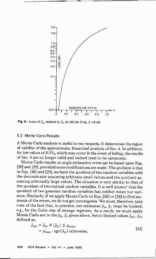
3.0-
2.0-
1.0- 0.8= 0.6- 0.5- 0.4- 0.3-
w 0.2- O J
0.1=
0.01 MONOPULSE RATIO
I 1 I 1 1 1 1 1 1 I'P 0.2 0.4 0.6 0.8 1.0
Fig. 6-Loss of ¡1 relative to be (in dB) for E/ No >_ 44 dB.
5.2 Monte Carlo Results
A Monte Carlo analysis is useful in two respects. It determines the region of validity of the approximate, linearized analysis of Sec. 4. In addition, for low values of E/No, which may occur in the event of fading, the results of Sec. 4 are no longer valid and indeed tend to he optimistic.
Monte Carlo results on angle estimation error can he based upon Eqs. 1261 and 129], provided some modifications are made. The problem is that in Eqs. [261 and 129], we have the quotient of two random variables with the denominator assuming arbitrary small values and the quotient as- suming arbitrarily large values. The situation is very similar to that of the quotient of two normal random variables. It is well known) that the quotient of two gaussian random variables has neither mean nor vari- ance. Similarly, if we apply Monte Carlo to Eqs. ]26] or 1291 to find mo- ments of the errors, we do not get convergence. We must, therefore, take note of the fact that, in practice, our estimates bp, be must he limited, e.g., by the finite size of storage registers. As a result, we must apply Monte Carlo not to the bp, Pc given above, but to limited values ipl,, Pcl, defined as:
%)p[ = np, if I Pp I
= Pmax sgn( bp) otherwise; 1331
224 RCA Review Vol. 41 June 1980

COMPARISON OF PHASE -ONLY
Pct = Pc, f I Pc I Pmax,
= Pmax sgn(Ic) otherwise. [341
Here /Pmax is the largest magnitude of l or ¡,c. that is computed or
stored. The introduction of Eqs. 1331 and [341 makes our results moderately
dependent upon the magnitude of Pmax.
In Table 1, we compare Monte Carlo data with the analytic expressions
given for app. The Monte Carlo results are based on the value Pmax = 2.0.
Note that for E/No >_ 14 dB, the analytical approximation is quite good.
Observe also that the linear approximation consistently underestimates app. Analogous results have been obtained for up,.
5.3 The Effects of Limiting on the Phase -Only Algorithm
A complete examination of the effects of limiting is tedious. However,
we have evaluated the special case of hard limiting at i -f for the mono -
pulse curve treated ín Sec. 5.2. The results are given in Table 2 as a
function of the signal to noise ratio (S/N) at i -f.
Table 2-Loss of Hard IF Limiting Relative to No Limiting.
S/N (dR) at IF loss in dR
-20 2
-10 2
0 2
10 0.8 90 0.0
5.4 An Alternative Procedure for Estimating u,,
In the above, we have obtained estimates of ír,, (1) by linearizing the expressions for p/, and 11c and (2) by using the Monte Carlo technique. An alternative procedure is to start from the expressions for ñ = U/V, obtain the probability density functions of numerator (U) and denom- inator (V) of j,, and then apply the methods outlined by C. C. Craig' to obtain the probability density function of the quotient (U/V). It is then
an easy matter to get the probability density functions of bp, p,.i. defined by Eqs. 1331 and [34[, respectively. Evaluation of app, apc. is then made
by numerical integration. Conceptually, and numerically, the Monte Carlo method is simpler.
RCA Review Vol. 41 June 1980 225
6. Conclusions
It has been shown that in the absence of limiting, the phase -only and the conventional monopulse algorithms give essentially identical results for E/No >_ 14 dB. With hard i -f limiting, however, the conventional monopulse cannot operate, while the phase -only algorithm suffers a loss relative to linear operation of 2 dB or less.
References:
C. C. Craig, "On Frequency Distributions of the Quotient and of the Product of Two Statistical Variables," Amer. Math. Monthly, 49, pp. 24-32 (1942).
226 RCA Review Vol. 41 June 1980

Ion Implantation of Sulfur and Silicon in GaAs*
S. G. Liu, E. C. Douglas, C. P. Wu, C. W. Magee, S. Y. Narayan, S. T. Jolly,
F. Kolondra, and S. Jain
RCA Laboratories, Princeton, NJ 08540
Abstract-This paper describes implantation of 28Si and 32S into semi -insulating GaAs to
generate high mobility n layers. Implantation of 28Si over an energy range of 40
keV to 1.2 MeV and fluence ranging from 1012 to 1016 cm -2 was studied. Implanted
layers were characterized by secondary ion mass spectrometry (SIMS), differential
Van der Pauw measurements, and differential CV measurements. A capless
thermal annealing technique under arsenic overpressure that results in high ac-
tivation efficiency and excellent surface morphology was developed. Implanted
n -layers as deep as 1µm have been realized.
The activation efficiency varies between 40 and 90% in the dose range between
3 X 10¹² and 5X 1013 cm -2 (implant energy 200 keV) and decreases toward the
high -dose level. A threshold fluence was observed below which the implanted
layer was no longer activated. This "cut off" dose depends on the substrate
characteristics and is typically 2 X 1012 cm -2 for 200 keV implant. Typical mo-
bilities at an electron density of 1-2 X 1017 cm -3 were 3500-4000 cri2/V-s. High
dose 1 X 1014 cm -2) Si -implanted semi -insulating GaAs after irradiation with
either a 0 -switched ruby laser or a Nd:Glass laser show higher sheet electron
concentration but lower mobility than thermally annealed samples.
The measured depth distribution of electron concentration is broader for S -
implanted than for Sí -implanted GaAs as a result of thermal diffusion during an-
nealing. The diffusion coefficients at 825°C for S and Si in GaAs were aeduced
from electron density p-ofiles to be 2-5 X 10-14 and _< i0-15 cm2/s, respectively.
The redistribution of the implanted Si following thermal or laser annealing was
studied using SIMS. Preliminary results on redistribution of Cr in the semi -insulating
GaAs due to implantation and annealing are also presented.
' This program was supported In part by the Office of Naval Research under Contract No. N00014- 78 -C-0367 and Defense Advanced Research Project Agency under Contract No. 00014-77-C-0542.
RCA Review Vol. 41 June 1980 227

1. Introduction
This paper describes the implantation of 28Si and 325 into semi -insu- lating (SI) GaAs substrates to generate uniformly -doped high -mobility n -layers. The activation of implanted donor atoms by thermal and pulsed laser annealing is also described. The characterization of the implanted layers by secondary ion mass spectrometry (SiMS), differential Van der Pauw measurements, and differential CV measurements is also dis- cussed. The significant achievements of this research are the first re- ported realization of implanted layers of 1µm thickness by using implant energies as high as 1.2 MeV and the development of a capless thermal annealing process under arsenic over -pressure that results in high acti- vation efficiency with excellent surface morphology.
Preliminary results show that laser annealing is more efficient than thermal annealing for high dose (>10" cm -2) implanted samples. The low sheet resistance layers obtained by laser annealing are particularly suitable for ohmic contact regions in discrete microwave devices like GaAs power field-effect transistors (FETs) and multigigahit-rate GaAs integrated circuits. It was observed, furthermore, that the redistribution of Cr from the Cr-doped semi -insulating (SI) GaAs substrate is sub- stantially lower for laser annealed than for thermally -annealed, high - dose implanted samples.
2. Substrates
Chromium -doped SI (100) -oriented GaAs substrates were used in our ion -implantation experiments. Studies were also made of implantation into vapor -phase grown, high -resistivity epitaxial layers. Semi -insulating substrates obtained from various sources were evaluated. Ion -implan- tation results depend strongly on the quality of the substrate material. Some SI GaAs substrates convert to either p -type or n -type following high -temperature annealing even in the absence of implanted ions. Substrate qualification is therefore mandatory prior to implantation. Our normal qualification test consists of implanting the sample with argon or krypton, then annealing at, typically, 80( to 950°C for 15 to 30 minutes. A qualified semi -insulating substrate does not convert after annealing.
Before ion implantation the SI substrates are carefully cleaned and etched to produce a damage -free surface. The wafers are cleaned in or- ganic solvents followed by I)I-water rinsing and a 5- to 10 -min etch in a solution of H9SO.1:H9O9:H2O in the ratio of 4:1:1. The wafers are then rinsed in I)I-water (> 14 M12) and spun dry. Etching is done in a tilted rotating beaker to obtain a uniformly etched surface. The layer removed
228 RCA Review Vol. 41 June 1980

ION IMPLANTATION
is approximately 3-6 pm. When implantation through a dielectric layer
is required, the wafer surface is coated with either a chemical -vapor -
deposited SiO2 layer or a reactively sputtered Si:1N4 layer. This layer
thickness is typically 500-700A.
3. Ion Implantation of 28Si* and 32S+ Into GaAs
Low -energy (<300 keV) ion -implantation experiments were performed
in the 300-keV machine at RCA Laboratories. Silane (Si H4) was used
as the source gas in the rf ion source for Si implantation, while solid sulfur
or H2S was used for S implantation. The beam current during Si im-
plantation is typically 0.1 µA for low -dose (1012 -1013 cm -2) and up to
10 pA for high -dose (1015 cm -2) implants. A typical implantation at 200
keV with a dose of 1 X 1014 cm -2 and a beam current of 10 pA takes about
1 min. The maximum beam current level attainable for S implantation
at 200 keV is about 5 µA. Implantation was studied at room temperature
with fluences between 1 X 10¹² and 5 X 1015 cm -2, and energies between
40 and 280 keV. High-energy (>5(0 keV) implantations were performed using a 3-MeV
Van de Graaff machine.` Silane (SiH4) was used as the source gas in the
ion source for Si implantation. The implantation energy ranged from
500 to 1200 keV. During implants the normal to the wafer was inclined
at an angle of 7° to the incident beam. High energy implant experiments
were done only with 28Si.
4. Thermal Annealing
One of the major problems of ion implantation into GaAs is that the
material begins to dissociate at the commonly used anneal temperatures
(800 1000°C). To prevent problems caused by dissociation, it is common
practice to use an encapsulant such as Si02,1 Si:4N4,2 A120:3,; AIN,4 the
combination of Si02 and Si;N4i5 or aluminum.6 We have developed an
operationally simple capless annealing process that results in high ac-
tivation efficiency with good surface morphology even for implants up
to 1 MeV. Capless anneal is done at a temperature between 80) and 900°C under
arsenic overpressure in an open quartz tube. The arsenic overpressure
at 850°C is maintained by using a flow of 75 ml of 7.5% AsH:, in 2 liters
of H2. Under this condition the arsenic overpressure at 850°C is over two
orders of magnitude higher than the equilibrium partial pressure.' The
arsenic overpressure prevents decomposition of GaAs and results in
' Located at Fusion Energy Corp., Princeton, NJ.
RCA Review Vol. 41 June 1980 229

excellent surface morphology. A higher AsH3 flow is used at 900°C to obtain thesame overpressure.
Anneal experiments were also performed on wafers encapsulated with a Si3N.t layer. A typical Si3N4 thickness was 2000-3001) A, and annealing was done in a N2 atmosphere. Both plasma -deposited Si3N4 layers and reactive -sputtered Si3N4 layers were tested. The plasma Si3N4 encap- sulated samples showed blisters following an 850°C 30 -min anneal; samples encapsulated with high quality sputtered Si3N4 showed no blistering up to 1000°C, and implanted layers were activated with good surface morphology.
5. Laser Annealing
We also studied annealing of Si -implanted GaAs using high -power pulsed Nd:Glass (X = 1.06 pm sub-handgap energy) and ruby (A = 0.694 pm-higher-than-bandgap energy) lasers. The laser system used was the Korad Model K-1500 gigawatt laser system.* This consists of an oscil- lator, amplifier, and a Pockel cell for Q -switching the oscillator output. Maximum output power is 1 GW/pulse at 2 pulse/min. The output pulse width was measured with a photodíode and a fast response oscilloscope. The optimum pulse shape recorded has a Gaussian distribution with a FWHM of 25 ns. The same laser system was modified for Nd:Glass laser experiments by replacing the laser rods and associated optics. The laser output pulse energy density was measured with a calibrated (±5%) ballistic thermopile. The laser output energy per pulse is adjusted by varying the high voltage on the xenon lamps around the amplifier stage and/or the oscillator stage.
6. Results 6.1 Thermally Annealed -Low Energy (<300 keV) Implanted Layers
Following implantation and annealing, the electrically active layer was characterized by Van der Pauw measurementss to determine the Hall mobility, sheet carrier concentration, conductivity, and activation ef- ficiency and by C- V measurements to determine the depth profile of the electrically activated donors. Characteristics of the low -energy (<300 keV) Si- and S -implanted GaAs wafers are described below.
(a) Mobility, Carrier Concentration, and Activation Efficiency
The Hall mobility and sheet carrier concentration of the electrically activated ion -implanted layer were measured by the Van der Pauw
' Hadron, Inc., Korad Div. Santa Monica, CA.
230 RCA Review Vol. 41 June 1980

ION IMPLANTATION
method.8 A square or a clover -shaped mesa sample with four ohmic
contacts at the corners was used. 'Typical sample dimensions were 7 X
7 to 10 X10 mm. The Hall mobility is given by
Rs ul=- Ill Ps
where Rs is the Hall coefficient and p, is the sheet resistance. The Hall
coefficient is given by
V24
R11;í
where 113 is the current, B is the magnetic flux density applied perpen-
dicular to the surface of the sample, and .S V. 4 ís the voltage change with
and without the magnetic field. The subscripts correspond to the four
ohmic contacts, which are numbered in sequence. The sheet resistance
p, is given by
ks = 108 121
V3 1 V23 131/s-2In2(112
141
where F is a geometrical correction factor. A relat ion between F and the
ratio (V34/112) to (V,;1/141) is given in Ref. 181. From Eq. III, the sheet
carrier concentration Ns is
1 Ns= -, 141
9Ks
where y is the electronic charge (1.6 X 10⁻¹⁹C).
The activation efficiency for an implanted and annealed sample is
given by
11 = Ñ7 151
where N;, is the fluence used. Table 1 shows results on 32S implantation into SI GaAs substrates and
into substrates with a high resistivity buffer layer grown by vapor phase
epitaxy. The implantations listed are for an energy of 200 keV and
fluences between 4 X 10i2 and 5 X 1014 cm -2. Table 2 lists results on
Si -implanted samples. All samples were annealed at 825°C for 20 min using the capless process. Mobility values are in the 300(1 to 4300 cm2/V-s
range, and activation efficiencies are in the 50 to 90% range for implants with fluences between 3 X 10¹² and 2 X 1013 cm -2.
'The lower activation occurring in high -dose implanted samples is
believed to be due to the solid solubility limit at the annealing temper-
ature. The mobilities are generally higher (4000 cm2/V-s) for im-
RCA Review Vol. 41 June 1980 231

Table I -S Implantation in GaAs.
Sample Number Substrate
Energy (keV)
Dose (cm -2)
Approx. Mobility Carrier Activation (cm2/V-s) Conc. (cm -3) Eft. (%)
62A SI 200 4.0 X 10¹² 3320 8.4 X 10¹⁶ 41.8 (MMG 103)
63BCr-n-/SI* 200 5.0 X 10¹² 4050 1.8 X 10¹⁷ 72.4 (A-141)
IOA SI (1.1)1
200 5.0 X 10¹² 3220 1.8x10¹⁷ 73.6
101) (5 -µmin -/S1* 2110 5.0 X 10¹² 4010 1.7 x 10¹⁷ 67.2 45A (3-µm)n-/SI* 250 7.0 X 10¹² 4360 1.4 X 10¹⁷ 40.9
(C265) 45E SI 250 7.0 X 10¹² 4070 1.5 X 10¹⁷ 46.9
(MX) 45F (10-µm)Cr-n-/S1* 250 7.0 X 10'2 4330 1.2 X 10¹⁷ 37.1
(A90) 19a SI 200 7.0 X 10¹³ 3220 3.7 x 10¹⁷ 73.0
(I.1)) 14C SI 200 1.5 X 10¹³ 3230 2.5 x 10¹⁷ 32.8
(I.1)1 64A SI 200 2.0 X 10¹³ 2900 5.8 X 10¹⁷ 58.3
(MMG10'2) 57 SI 200 1.0 X 10¹⁴ 3200 1.5 x 10¹⁸ 30.6
( X S3761) 50A SI 200 5.0 x 10¹⁴ 2890 1.7 X 10¹⁸ 6.7
(\S3761 F)
Vapor -phase high -resistivity epitaxial layer grown on SI substrate.
plantation into a high -quality, high -resistivity epitaxial buffer layer grown on a SI GaAs substrate, as shown in Tables 1 and 2. A direct implant into some substrates (e.g., sample A26) also results in electron mobility of higher than 4000 cm2/V-s at 1-2 X 10'7 cm -3 doping den- sity.
The carrier concentration values in Tables 1 and 2 were approximately determined using
Ns Nm- .
2a.SRe This expression is an approximation to the Gaussian distribution
Ns = 5N(x,E)dx =N,,, ._Rn V 9
X I I + led' RI,
N/ISRp '
where RI, and Rj, are the projected range and standard deviation, re- spectively. The measured sheet electron concentration values were used for Ns in F,q. 161, and the ..5/If, was taken as 0.08µm at the 200-keV en- ergy level. This value of RI. is close to that measured by SIMS. Table :3 lists computed data using the electronic stopping powers compiled by
181
[71
232 RCA Review Vol. 41 June 1980

ION IMPLANTATION
Table 2 -Si Implantation in GaAs.
Sample Number Substrate
Energy (keV)
Dose (cm -2)
Mobility (cm2N-s)
Approx. Carrier
Conc. (cm -3) Activation
Eft'. (%)
A24A 6-µmn'/SI* (1)95)
200 3.0 x 10¹² 4290 8.2X 10¹⁸ 54.9
A35A SI (XS3761)
200 70
3.0 x 10¹² 1.5 x 10¹²
3370 1.9 x 10¹⁷ 82.6
A35C SI (XS3765F)
200 70
3.0 x 10¹² 1.5 x 10¹²
3630 1.7 x 10¹⁷ 76.8
A351) 5- n143) I* 270
00 3.5 x 10¹²
4000 1.9 x 10'7 85.1
A28N SI 200 3.5 x 10¹² 3740 1.6 X 10¹⁷ 90.3
(\S3761 F')
A23A Cr-n-/SI* 200 4.0 x 10¹² 3930 1.2 X 10¹⁷ 60.5
1A156) A3A SI 200 4.0 x 10¹² 3570 1.2 x 10¹⁷ 62.0
(MMG102) A26 SI
(XS3765) 200
50 4.0 x 10¹²
2.0 X 10¹² 4000 1.5 x 10¹⁷ 60.5
A4B SI 200 6.0 x 10¹² 3220 1.9 X 10¹⁷ 64.7 (\53761)
A31 SI 200 2.0 x 10¹³ 2930 7.0 x 10'7 70.1
(XS3761) A6 SI 200 5.0 X 10¹³ 2050 1.1 X 10¹⁸ 37.0
(MM 5102) A34 SI 200 1.0 X 10¹¹ 2200 I.I X 1018 21.5
(\S3761 F) A44 SI 70 1.0 X 10¹⁵ 1770 1.6 X 10¹⁸ 3.2
(XS3761 F)
* Vapor -phase high -resistivity epitaxial layer grown on SI substrate.
Northcliffe and Schilling9 instead of values predicted by LSS
theory.10 'I'he mobility versus carrier concentration data for 5- and Si -implanted
samples are shown in Figs. 1 and 2, respectively. Theoretical curves of
drift mobility with compensation ratio as parameter are also included)' Most of the experimental points are located between a compensation
ratio of 1 and 2, indicating acceptable material quality. Experimental carrier concentration data (electrically activated) as
function of implantation dose are shown in Figs. 3(a) and 3(h) for S and
Si implantation, respectively, into GaAs. The samples were capless-
annealed at a temperature of 825°C for 20 min. The implantation energy
was 200 keV for all data points. Data -point scattering for different substrates is apparent. Both the Si- and S -implantation data indicate
that (1) the carrier concentration varies almost linearly with fluence for
fluences between 5 X 10¹² and 3 X 101s cm -2 for S implant and between
2.5 X 10¹² and 2 X 1013 cm -2 for Si implant and (2) free carrier concen-
tration increases at a much slower rate at high f1uence. We will .show later
that higher activation at high doses can be obtained by laser annealing.
Similar saturation effects for Se and S implantation have been reported
by 1)onnelly.12 The data also show that no electrical activation was
RCA Review Vol. 41 June 1980 233

8000
> 6000
E
1 4000
I-
J EIS
O
2000
11111111111111111111111111 1 III I
1016 1017 1016
FREE ELECTRON CONCENTRATION, n (cm -3)
Fig. 1-Mobility versus carrier concentration for S implanted in GaAs.
1019
achieved at fluences lower than about 1012 cm -2 (200 keV). This "cut-off" threshold varies with substrate quality. This cut-off behavior is not fully understood.
8000
6000
4000
2000
1 I 1 II IITII Si -IMPLANTATION IN GoAs
N'+N -10
1 I 1 I 11 1 1 I I 1 1 11 1 1 1 1 1 1 11 015 1016 1017
1018
FREE ELECTRON CONCENTRATION, n (cm -3)
Fig. 2-Mobility versus carrier concentration for Si implanted in GaAs.
1019
234 RCA Review Vol. 41 June 1980

ION IMPLANTATION
1019 1019.
S -IMPLANT IN Go As
a 5. -IMP -ANT IN GaAs
SUBSTRATES: SUBSTRATES: CRYSTAL SPECIALTIES CRYSTAL SPECIALTIES MITSUBISHI MONSANTO - MITSUBISHI -MONSANTO LASER DIODE LAB
/ / /
1O1B / / 1048 - / / / /
É
/ E
z
1017
/ // z
1017-
/ i : 6 s
/
1016 1.1012
1016
1.1012 I1013 IIO' 11015 101013 1.101 IIOIS DOSE (cm -2) DOSE (cm -21
(o) (b)
Fig. 3-Carrier concentration as a function of implantation dose (a) for S implantation and
(b) for Si implantation into GaAs.
(b) Electrical Conductivity of Ion -Implantation Created Disordered Layer
The surface of an as -implanted SI GaAs substrate shows electrical conduct ion due to lattice disorder. The sheet conductivity is a function of implantation dose. This phenomenon has been discussed by Y. Kato, et al.) I The sheet resistance of as -implanted GaAs was measured by a four -point probe. Ohmic characteristics were obtained with probes on as -implanted GaAs surfaces. Figs. 4(a) and (b) show the variation of sheet
á io to \ Ó
1 06 be
W \V 2 e a IA
á \Ps-308x1023N-139In
IDS W w 2 to 6'----o-2-0-
107 I r -r lTTrr) I I T n TIT -r-r-rTTlrr S - IMPLANTED Ga As
o CRYSTAL SPECIALTIES a LASER DIODES
MITSUBISHI MONSANTO A TYPE IV SUMITOMO
MORGAN
104 I I I 1 I fI) I I 1 11Iu1 I I I
1012 1013 10'4 1015
IMPLANTATION FLUENCE (Cm -2)
107
106
105
104 1012
T-T7-11TIT) I r I Ill Ti) I I I IITrt
1.0
\e
SI -IMPLANTED Go As
A CRYSTAL SPECIALTIES MORGAN
o MITSUBISHI MONSANTO \ Ps=746x10'RN'179
' 1111111 I ' 1 I'teee ! 1 1 11111
1013 IC" 1015
IMPLANTATION FLUENCE (Cm -2 )
(a) (b)
Fig. 4-Sheet resistance versus implant dose measured (a) on S implanted and (b) on Si
implanted unannealed GaAs.
RCA Review Vol. 41 June 1980 235

resistance with dose for S and Si implants into a number of SI GaAs substrates. In the dose range of 2 X 10j2 to 3 X 1013 cm -2, the sheet re- sistance decreases with increasing dose approximately as
ps = 3.08 x 10²³ x N-1.39 [8)
for S implantation, and
ps = 7.46 X 1028 N-1.79 I9)
for Si implantation. Above 5 X 1013 cm -2 fluence, electrical conductivity begins to saturate.
A reduction in conductivity is observed as the dose increases beyond 1015 cm -2. These features are in general agreement with Kato, but the ex- ponent dependence of ps on N given by Eqs. 181 and 191 is considerably less steep (-1.39 and -1.79 versus -3).
Note the qualitative correlations between the electrical conductivity of disordered layer following implantation as shown in Figs. 4(a) and (h), the electrically active sheet carrier concentration following annealing, as shown in Figs. 3(a) and (b). Both sets of figures show a knee at a dose of about 5 X 1013 cm -2 and an exponentially related region between about 2 X 10'22 and 3 X 1013 cm -2. The conductivity of as -implanted layers can be used to conveniently monitor implantation before an- nealing.
(c) Depth Distribution of Electron Concentration
The electron concentration was measured by the well known technique of making CV measurements on a Schottky diode defined on the im- planted layer.14 The accuracy of the CV technique is inherently limited in reproducing a shallow electron density profile with a steep doping
Table 3 -Range and Straggle St at ist ics for 325 and 285i Ions Implanted Into GaAs.
Energy (keV)
S in GaAs RP
(pm) JR), (pm)
Energy (keV)
Si in GaAs R),
(pm) .ARP (pm)
IO 0.0102 0.0078 10 0.0111 0.0105 50 0.0395 0.0194 50 0.0441 0.0221 70 0.0537 0.0252 70 0.0605 0.0288
101) 0.0758 0.0337 10(1 0.0861 0.0383 120 0.09(18 0.0390 120 0.1033 0.0442 150 0.1135 0.0165 150 0.1291 0.(1523 2(1(1 0.1515 0.0578 200 0.1723 0.1)646 260 0.1973 0.0702 260 0.2242 0.1)778 300 0.2279 0.0778 300 0.9582 0.0855 40(1 0.3029 0.0942 400 0.3421 0.1024 600 0.4506 0.1213 6(10 0..a /53 0.1296 81111 0.5919 0.1423 800 0.6549 0.1488
1000 0.7219 0.1580 10(10 0.7941 0.1638
236 RCA Review Vol. 41 June 1980

ION IMPLANTATION
density variation.75 The inaccuracy occurs particularly close to the surface and toward the tail end. For most implantations performed, the ratio of Rp/.. Rp is about 2 (Table 3), which means a less steep variation in doping densities than for implantations into silicon. The CV technique thus provides information around the peak of the depth distribution.
Fig. 5(a) shows the carrier concentration density profile of a Si -im- planted sample. The implantation dose and energy level are 3.5 X 10¹²
cm -2 and 200 keV, respectively. Fig. 5(b) shows the carrier -concentration density profile of a multiple Si -implanted sample. The dose and energy levels are 3 X 10L2 cm -2 at 200 keV, and I x 1012 cm -2 at 70 keV. These values were chosen to yield a nearly constant doping distribution. Fig. 5(b) demonstrates that the (loping profile can be controlled by multiple implants.
The measured electron distribution of S -implanted GaAs was found to be broader than for similar Si -implanted samples and deviates from a Gaussian distribution. This is attributed to significant diffusion during anneal. Fig. 6 shows a measured curve with circles indicating the com- puted I,SS distribution, including thermal diffusion, normalized to match the measured peak. The diffusion coefficient, 1), corresponding
1018
SAMPLE A49A (Si -IMPLANTED) 200 keV
3.5v 1012 cm -2
825C 20min ANNEAL
101
1016
10150 l I I I I
01 0.2 0.3 0.4 05 06
(p.m) (o)
1018
1016-
10 0 0.1
SAMPLE A60B (Si -IMPLANTED) 3. 10i2 cm -z 250keV
I x 10i2 or. -2, 70 keV
1
0.2 0.3
.lµm) (O1
0.4 0.5 06
Fig. 5-Carrier concentration profile (a) for single -energy Si implant and (b) for dual Si im-
plant.
RCA Review Vol. 41 June 1980 237

1017
1016
1015
I t I 1
SAMPLE IOC
(S - IMPLANTED) 200 key 5x 10¹² -2
825 20 mir ANNEAL
I I I I
o 0.3
x (p.m)
Fig. 6-Measured electron density distribution of S implanted GaAs.
0.1 0.2 0.4 0.5 06
to the 825°C anneal temperature was deduced to he 5 X 10-14 cm2/s. Similar measurements on a number of samples show values of I) between 2 X 10-14 and 5 X 10-14 cm2/s at 825°C. This compares favorably with that measured by Young and Pearson16 and by Asai and Kodera17 hut is almost an order of magnitude lower than Kendall's result.18 A similar match to I.SS distribution was made for the measured profile on Si - implanted GaAs samples and the diffusion coefficient was found to he 510-15 cm2/s.
(d) Electron Concentration and Hall Mobility Profile
The depth distribution of carrier concentration and mobility on some samples were determined by Van der Pauw measurements in conjunction with controlled layer removal.
The mobility, µ, and carrier concentration density, n, corresponding
238 RCA Review Vol. 41 June 1980

ION IMPLANTATION
to the ith chemically removed GaAs layer are given respectively by 19,20
(R.s/p4)i-1 - (Rs/P. )i
- (1/MA--1 - (1/p.)i 10I
(1/P5)i-1 - (l/Ps)i [1 l I.
nI 004 where p.,. is the sheet resistivity, Rs is the sheet Hall coefficient, h the
thickness of the chemically removed layer, y the electrical charge, and
the lower case index i and i - 1 refer to the successive order of removed
layers. The sheet resistivity p, and Hall coefficient Rs are given, re-
spectively, by Eqs. 131 and ]2]. Fig. 7 shows the carrier concentration and mobility profile of a 5 -
implanted sample (49B). This sample was implanted with a dose of 1013
cm -2 at 200 keV. Post -implant annealing was done at 825°C for 20 min under arsenic overpressure. The profile shows a maximum carrier con-
centration of 2.4 X 1017 cm -3 which agrees with that obtained by CV measurement. The mobility profile varies from 3000 cm2/V-s at the
surface to over 4000 cm2/V-s toward the SI substrate, which agrees with the measured average mobility of 3520 cm2/V-s for the entire layer. The profile deduced from CV measurement after normalization in carrier
1018
17 IO
16 10
0
SAMPLE 49B (S-IMPLANTED) 200 KeV, 1a 1013cm 2
825"C. 20 MIN ANNEAL
0.1 0.2 0.3 z(µm)
0.4
3000 1.
2000
1000 0.5
Fig. 7-Carrier concentration and mobility profile of a S implanted sample.
RCA Review Vol. 41 June 1980 239

19
10
~E - le z 10 o á
z W U 2 O u
¢
K Q 17 U 10
16
10 o 0.1
SAMPLE A90 (Si -IMPLANTED) I a 1015cm 2
70 keV 825°C 20 min ANNEALED
02 DEPTH lµm)
0.3
Fig. 8-Carrier concentration and mobility profile of a Si implanted wafer, 70 keV.
concentration matches well with the profile measured by differential Van der Pauw measurement. The normalized points are indicated by crosses in Fig. 7. Roth cases are for S implantation at 200 keV with dif- ferent implant doses. The carrier concentration and mobility profiles of a high -dose Si -implanted GaAs wafer is shown in Fig. 8. The average mobility and sheet carrier concentration of the wafer are 1800 cm2/V-s and 2.14 X 10'1 cm -2, respectively.
(e) Electron Concentration and Drift Mobility Profile
Pucel and Krumm2' have shown that the depth distribution of the drift mobility of a semiconductor layer on an SI substrate can he measured by a long -gate FET fabricated thereon. This technique measures the transconductance g,,, and the capacitance C,,, under various gate -bias voltage. At a given gate bias voltage, the drift mobility µd is given by
g,N 9 µd=- 112 Cg Vdd
where L is the gate length and Vdd the do voltage between the source and drain.
240 RCA Review Vol. 41 June 1980

ION IMPLANTATION
lo
10
! 7
02 04 06 08 xl lam l
S -IMPLANT
OHMIC
Fig. 9-Drift mobility and electron density profile of a S implanted GaAs wafer.
The depth x corresponding to this mobility value is
EWL a Cg
where E is the dielectric constant and W, L, are the width and length of the gate, respectively. Using the capacitance versus gate bias data, the
carrier concentration profile can be simultaneously determined. Fig. 9 shows an example of drift mobility and electron density profile
of a S -implanted sample. The drift mobility varies between 25(0 cm2/V-s
toward the surface and 3800 cm2/V-s toward the substrate. The effective
Hall mobility for the sample was 3250 cm2/V-s. The ratio of Hall to drift mobility is thus close to unity. The sample was S -implanted at 200 keV
with a fluence of 1 X 1013 cm -2 and annealed at 825°C for 20 min- utes.
(f) Impurity Atom Concentration Profile
1131
The measurements described so far give information on the depth dis-
tribution of charge carriers associated with electrically active centers
and not necessarily the true range distribution of the implanted atoms.
The true impurity atom distribution was measured by secondary ion
mass spectrometry (SIMS). Figs. 10 and 11 show, respectively, SIMS
RCA Review Vol. 41 June 1980 241

Io20
ID 10
18
10
S -IMPLANT 250 keV
1x1015cm-2
10 1 -
116 0 : .
15[ 10 I t I t 0 0.2 0.4 0.6 0.8 1.0
DEPTH ( micrometers )
Fig. 10-SIMS profile of S implant made at energy of 250 keV with fluence of 1 X 1015 cm -2.
S. Go As
40 keV
120keV
200 keV
280 keV
1.0 c2
DEPTH (µm)
Fig. 11-SIMS profiles of Si implants made at energies of 40, 120, 200, and 280 keV.
242 RCA Review Vol. 41 June 1980

ION IMPLANTATION
profiles of a S -implanted and a number of Si -implanted samples. The distribution is approximately Gaussian except with a broad tail. The projected range and straggle values for Si implantation in GaAs deduced from SIMS are discussed later.
6.2 High Energy (1.2 MeV) 28Si Implantation-Thermal Annealing
The profiles and range statistics of 28Si implants in GaAs up to 1.2 MeV have been analyzed using SIMS. Based on the information obtained, uniformly -doped "28Si profiles 1 -pm deep have been produced in GaAs using multiple implants. This section discusses the implanted profiles, dopant activation analyses, and mobility measurements on implanted (single or multiple) and annealed GaAs wafers.
(a) Atomic Profiles-Range Statistics
Fig. 12 shows the SIMS profiles of a series of single -energy implants made over a range of 0.7 to 1.2 MeV. Note that the profiles are not Gaussian in shape but are noticeably skewed. A theory developed by Karl Pearson22,23 and applied to "B implants into Si at energies up to 8(K) keV by Hofker24 makes use of the first four experimental moments to produce fits to the observed profiles. From these calculations, the range Rp and straggle .ARP, can be obtained for skewed data.
Fig. 12-SIMS profiles of implants made at energies of 0.7, 0.8, 0.9, 1.0, and 1.2 MeV.
RCA Review Vol. 41 June 1980 243
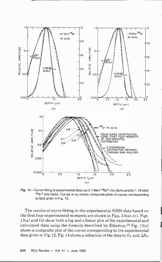
1.0
0.01
0.001
0.5
05 10 1.5
DEPTH (µm)
It))
eV 28Si' IN Go As
1.0 1.5
DEPTH (µm)
(c)
20
SOLID CURVE CONSTRUCTED USING FIRST FOUR MOMENTS OF EXPERIMENTAL DISTRIBUTION
EXPERIMENTAL DISTRIBUTION OBTAINED
THROUGH SIMS ANALYSIS
\ \\
2.0 2.5
Fig. 13-Curve-fitting to experimental data: (a) 0.7-MeV 28Si+ into GaAs and (b) 1.18-MeV 28Si+ into GaAs. Curves in (c) shows composite plots of curves corresponding to data given in Fig. 12.
The results of curve fitting to the experimental SIMS data based on the first four experimental moments are shown in Figs. 13(a)-(c). Figs. 13(a) and (b) show both a log and a linear plot of the experimental and calculated data using the formula described by Elderton.2; Fig. 13(c) shows a composite plot of the curves corresponding to the experimental data given in Fig. 12. Fig. 14 shows a reduction of the data to Bp and ..5Rp
244 RCA Review Vol. 41 June 1980
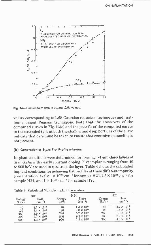
ION IMPLANTATION
12
1.0
0.8 E
re
< 0.6
04
02
Rp
X ABSCISSA FOR DISTRIBUTION PEAK
CALCULATED MODE OF DISTRIBUTION
R
0 1/2 - WIDTH AT 0.606 N MAX /X STD DEV OF DISTRIBUTION x ..
x' /
Rp ,/ /
/ /
/ /
x/ ARp
-e--e--s--s--- , --O'
0.2 0.4 0.6 0.8 1.0 1.2
ENERGY (MeV)
Fig. 14-Reduction of data to RP and .5 RP values.
values corresponding to LSS Gaussian reduction techniques and first - four -moment Pearson techniques. Note that the crossovers of the computed curves in Fig. 13(c) and the poor fit of the computed curves to the extended tails at both the shallow and deep portions of the curve indicate that care must be taken to ensure that excessive channeling is
not present.
(b) Generation of 1-µm Flat Profile n -layers
Implant conditions were determined for forming -1 -pm -deep layers of Si in GaAs with nearly constant doping. Five implants ranging from 40
to 900 keV are used to construct the layer. Table 4 shows the calculated implant conditions for achieving flat profiles at three different impurity concentration levels: 1 X 1020 cm -3 for sample H23, 2.5 X 1019 cm -3 for sample H24, and 1 X 1019 cm -3 for sample H25.
Table 4-Calculated Multiple Implant Parameters.
H23 H24 H25 Energy (ke% )
1)ose (cm -2)
Energy (keV)
1)ose
(m
Energy (keV) (keV)
Dose tcm-2)
40 4.7X10¹⁴ 40 1.4X10¹⁴ 40 4.7X10¹³ 120 1.4 X 10¹⁵ 120 4.0 X 10¹⁴ 120 1.4X10¹³ 280 1.9 X 10¹⁵ 280 5.7 x 10¹⁴ 280 1.9 x 10¹⁴
500 2.7 X 10¹⁵ 500 8.2 X 10¹⁴ 500 2.7 X 10¹⁴
900 4.3 X 10¹⁵ 900 1.3 X 10¹⁵ 900 4.3 x 10¹⁴
RCA Review Vol. 41 June 1980 245

1022
1020
1016
101
CALCULATED PROFILE SIMS
EXPERIMENTALLY MEASURED PROFILE
0.0 0.5 IA 1.5
DEPTH OF Si INTO GaAs (µm)
Fig. 15-Comparison of calculated and actual SIMS profiles.
Table 5-Implant Conditions for Flat Profile of Si in GaAs.
2.0 2.5
Energy (keV) Parameter 40 120 280 501) 900
(cm -2) 4.70 X 10¹⁴ 1.35 x 10¹⁵ 1.90 X 10¹⁵ 2.73 x 10¹⁵ 4.33 X 10¹⁵
Dose No. 303.6 872.0 1227.0 550.2 872.6 Scale 6 X 10⁻⁶ 6 X 10⁻⁵ 6 X 10⁻⁶ 6X10⁻⁶ 6X10_6
Area = 24.19 cm2 Area = 7.56 cm2 (Labs machine) (FEC machine)
A comparison of the calculated plot* and the measured SIMS profile is given in Fig. 15. Implantation data are shown in 'Fable 5.
(c) Mobility, Carrier Concentration, and Activation Efficiency
Following thermal annealing, the electrical characteristics of the high- energy implanted n -layers were evaluated by Van der Pauw measure- tnents.8 Table 6 shows the measured sheet carrier concentration N sheet resistance p.,, Hall mobility µ, and the activation efficiency )), for 1-MeV Si -implanted GaAs. The implanted Si doses varied between 1.5 X 10¹³ and 5 X 1015 cm -22. The mobilities and activation efficiencies
' The calculated data were made using conventional LSS Rp and ,RP values because at the time of calculation, the Pearson four -moment -curve fits had not yet been investigated.
246 RCA Review Vol. 41 June 1980

ION IMPLANTATION
Table 6-I-11eV Si Implantation in GaAs.
Sample No. Dose (cm -2) N, (cm -2) p (1l/0) p (cm2/V-s) )7(%)
H15 5.0 X 10¹⁵ 3.7 x 10¹³ 85 2000 0.7
H16 1.5X10¹⁵ 5.7X10¹³ 65 1690 3.8 H17 5.0 X 101° 7.3 X 10¹³ 49 1760 14.7
H18 1.5 X 10¹⁴ 4.6 x 10¹³ 52 2620 30.8 1119 5.0 x 10¹³ 2.7 X 10¹³ 70 3310 54.2 H20 1.5 X 10¹³ 1.1 X 10¹³ 142 3980 73.5
obtained are either comparable to or better t han those obtained with low -energy implantation at, comparable dose levels (Table 2). The mo-
bilities are in the range of 1690 cm2/V-s for high -dose implanted samples
to 3980 cm2/V-s for low -dose implanted samples; the activation ef- ficiencies are in the range of below 1% for high -dose implanted samples to over 73% for low -dose implanted samples. All data shown in Table 6
are for samples capless-annealed at 825°C for 20 min. The activation efficiency of heavily implanted samples increased át
a higher annealing temperature. This result is shown in Table 7 where
Si -implanted wafers were annealed at two different temperatures, 825
and 970°C. The two samples annealed at 970°C give rise to a higher ac-
tivation efficiency. The annealing was done in a N2 atmosphere with samples encapsulated with 2000 -A -thick reactively sputtered Si3N4.
Fig. 16 shows the measured sheet carrier concentration as a function of dose for samples implanted at 200 keV and 1 MeV and annealed thermally at 825°C for 20 min. The I MeV implanted samples showed a substantially higher sheet carrier concentration in the close range of 5 X 10¹³ to 2 X 101' cm -2. This is because, at a given dose level, the 1 MeV implant results in a lower impurity concentration distribution than that of the 200 keV implantation, because of its higher straggle. The drop in
the sheet carrier concentration at high -doses is not fully understood.
Table 7 -Results of Si -Implanted Wafers at 825 and 970°C.
Sample No. Parameters HIO HII
Energy (keV) 900 I000 Dose (cm -2) 3.0 X 10¹⁵ 3.1 X 10¹⁵
Anneal Temp. (°C) 825 970 825 970 N. (cm -2) 4.2 X 10¹³ 2.1 X 10¹⁴ 3.7 X 10¹³ 1.5 X 10¹⁴
p.(12/01 84 22 93 27
p (cm2/V-s) 1800 1320 1810 1550
v (%) 1.4 7.1 1.2 4.7
RCA Review Vol. 41 June 1980 247

E
2.10" z z o
IY
z w u O 1 013
¢
¢
N 1 012
1012
1 1 1 1 1 1 1 1 1 1 1 1 1 1 111 I r 1 1 1 rrll 1 i i 1 111
--IMeV IMPLANT o--
- --- 200 KeV IMPLANT 825°C,20min ANNEAL /
// w
=100 % ../ .6'
o
I I I 11111 1 1 1 1 1 l I. 1 1 1 1 1 1 1 1 1 I 1 1 t ill 1013
1012.
IMPLANT DOSE No(cm )
1015 1016
Fig. 16-Measured sheet carrier concentration as a function of dose in Si implanted samples at 200 keV and 1 MeV.
(d) Carrier Concentration Distribution
The electron density profiles of high -energy -implanted thermally - annealed samples were evaluated using differential CV measurements in conjunction with controlled layer removal. Figs. 17 and 18 show typical electron concentration distributions. Fig. I7 is for samples implanted at an energy level of 1 MeV, with fluences of 5 X 10¹³ (H 19) and 1.5 X 1013 cm -2 (H20). A SIMS profile of a high dose (5 x 10'4 cm -2), 1 MeV implanted unannealed sample is also shown in Fig. 17 to provide a ref- erence. Fig. 18 shows the profile of a multiple -implanted sample designed
1019
1016
1017
10 o
16
ELECTRON CONCENTRATION PRO FILE
1 111
0.4 0.8 1.2
DEPTH (µm)
Fig. 17-Profiles of 1 MeV Si implanted GaAs.
1.6 20
248 RCA Review Vol. 41 June 1980

ION IMPLANTATION
18
lo
E
z z o
17
tr 10 I-
z w U z o U
2 W
Ir 4 U
16
10 0
SAMPLE 1127
MULTIPLE , SI- IMPLANT IN GaAs
40,- 900 KeV
4.7 a I012'- 4.3 a 1013cm-2
MOBILITY: 3007 cm2/V-s
1 I I 1
0.2 0.4 0.6 0.8 DEPTH ( p.m
1 -
1.0 1.2 1.4
Fig. 18-Carrier concentration of a multiple -implanted sample.
to produce a 1 -pm flat prof le with a maximum impurity concentration of I X 1018 cm-;. The implant parameters are the same as those shown in Table 5, only the fluences are two orders of magnitude lower. These were samples capless-annealed at 825°C for 20 min. under arsenic over -pressure.
The shape of the profiles show reasonable agreement with the SIMS measurements made on high -dose implanted unannealed samples. The differences ill range and standard deviation are approximately within 10% on the 1-MeV single energy implanted samples. 'I'he deviations between the multiple -implanted profiles determined by the SIMS (Fig.
15) and the CV measurement (Fig. 18) are greater. This is expected be-
cause the CV measurement determines the electrically active carrier concentration distribution and the activation efficiency varies with dose and energy. A better match can be obtained by including the dose - and -energy -dependent activation efficiency in flat -profile design.
6.3 Pulsed Nd:Glass Laser Annealing
Semi -insulating (100) GaAs substrates were implanted with 28Si+ at energies between 70 and 200 keV and !Thence between 3 X 10¹² and 3 X
RCA Review Vol. 41 June 1980 249

L { 1 1 1 111 I X I I I TTTr 1.0
1.17x
LASER x - ANNEAL-.., /x 0.50 _
z -
z .-
rc // , r. - / z _ / w / ,A---- uz / O / y 825°C '-'1013,r- / / 20 min
w - 9=100°h /' _ - E // x 0.68 J/tm2 ¢ -
ú /:/ / - I.- / La / / _ - /. N // / / I I 111till I IIIIIII I I IImil I I 111111
1013 1014 1015 1016
IMPLANT DOSE (cm -21
101
Fig. 19-Comparison of thermal and laser annealing: a 1.C6 -µm, 25-ns single pulse (Nd: Glass) laser was used.
1015 cm -2. Some substrates were polished on both sides to facilitate optical absorption studies. Following implantation, the 0.04 cm -thick wafer was cleaved to samples between 0.5 and 2.0 cm2 for laser -annealing experiments.
'1'he Nd:Glass laser was operated at an output energy density of be- tween 0.2 and 2.5.1/cm2 per pulse. The corresponding power density lies between 8 and 200 MW/cm2. The laser diameter is 2 cm. Thermally annealed samples used as control were annealed at 825°C for 20 min. under arsenic overpressure.
Fig. 19 shows comparative results of sheet carrier concentration density for Nd:Glass laser and thermally annealed samples for implanted 28Si doses between 3 X 10¹² and 3 X 1015 cm -2. The energy density of each laser pulse used is indicated by crosses and varies between 0.5 and 1.17 .1/cm2. All experiments used single pulses. At low laser energy density the implanted layers were only partially activated.
'fable 8 lists comparative results on mobility, sheet carrier concen- tration, and activation efficiency for Si -implanted GaAs annealed using Nd:Glass laser and thermally. The fluences are greater than 3 X 1011 cm -2. The laser -annealed samples showed higher activation efficiencies and lower mobility than thermally annealed samples.
The optical absorption in the sample was measured by spectropho- tomet ry. The transmission through the sample and the reflect ion from the sample were measured on a Cary spectrometer in the 7000- to
250 RCA Review Vol. 41 June 1980
1

ION IMPLANTATION
Table 8 -Comparison of Thermal and Nd:Glass Laser Annealing Data.
Si Implantation Dose (cm -2) 3.0 X I015 3.0 X 10¹⁵ 1.0 X 10'5 5/2 X 10'4 3.0 X 10'4 Energy (keV) 70 2(N) 70 200/70 200
Nd:Glass Laser Annealing Energy (.1/ 1.00
cm 1)
2.25 0.34 1.17 0.68
Na (cm -2) 1.91 X 10¹⁴ 1.45 X 10¹⁴ 6.55 X 10¹³ 1.25 X 101' 4.60 X 10'3 µ (cm2N-s) 250 1020 250 530 520 r) (%) 6.4 4.8 6.6 17.9 15.3
Thermal Annealing N. (cm -2) 5.1 X 10¹³ 3.3 X 10¹³ 3.2 X 10¹³ 2.8 x 10¹³ 3.0X 10¹³
µ (cm2/V-s) 1390 1910 1770 1880 1540
>l (%) 1.7 1.1 3.2 4.0 10.0
12000-A wavelength range_ The absorption at a given wavelength (e.g.,
1.06 µm) is calculated by the expression:
A = 1 -T - I?
where A, T, and R are respectively, absorption, transmission, and re-
flection which are all absolute values and are expressed in percentages.
The enhanced absorption clue to implantation damage is equal to A - A0, where A0 is the absorption through the unimplanted sample. At 1.06 -pm wavelength, the measured value of An was typically 0.1. The reflectance was measured with reference to an aluminum mirror and the
absolute value obtained through calibration. Fig. 20 shows the reflectance measured on an as -implanted wafer and
06
05
06
05 R=0 351
o
0 4
ó
04
¢ O
o O
03 A44
-6 u O J
03
1x10¹⁵ Si /cm2 70 keV
02 AS IMPLANTED 02
0I 01
o o 8000 12,000 6000
R =0 390
33F LASER ANNEALED
0 34 J/cm2
8000
a lAl (b)
10,000 12,000
Fig. 20 -Reflectance measured (a) on art as -implanted wafer and (b) after laser an-
nealing.
RCA Review Vol. 41 June 1980 251

on the same wafer irradiated with a Nd:Glass laser pulse at an energy density of 0.34.1/cm2. Because of the enhanced absorption in the high - dose implanted layer, the reflection is affected only by the front (im- planted) surface. Consequently, the reflectance forms a continuous line as it passes through the absorption edge as shown in Fig. 20(a). For the annealed samples, restored lattice order reduces the enhanced absorption in the implanted layer. The reflectance spectrum thus forms a step. as shown in Fig. 20(h), as the wavelength passes through the hand edge of GaAs, because the reflection is enhanced in the long wavelength range due to multiple reflection from the polished sample hack surface. The multiple reflection dominates over the change in surface reflectivity which occurs as a result of implantation.
The transmittance through an ion -implanted sample before and after annealing is shown in Fig. 21. The gradual increase in absorption from the long -wavelength side toward the absorption edge in the as -implanted sample is a band -tailing effect produced by impurities.25 The trans- mittance at 1.06 -pm wavelength changes from 0.170 for the as -implanted sample to 0.457 after laser annealing at 0.68.1/cm2. The enhanced ah-
io
09
08
0 7
06
O cº
05
04
03
0.2 8000 9000 1000 1100 1200
>f 4 1
Fig. 21-Optical transmission from Si -implanted GaAs sample annealed at different laser energy densities.
252 RCA Review Vol. 41 June 1980

ION IMPLANTATION
1013 1014
IMPLANT DOSE No(cm2)
Fig. 22-Measured values of transmittance (7), reflectance (R), and enhanced absorption
(A - A°) for different dose levels.
sorption (A - An) can he evaluated from the expression given in the
previous section. Fig. 22 shows the measured values of transmittance, reflectance, and enhanced absorption for as -implanted samples at dif- ferent close levels.
Optical absorption measurements show that the implantation -en-
hanced absorpt ion at a given wavelength (e.g., 1.06 pm) below the hand
edge increases with implant close. This enhanced absorption is greatly reduced following annealing as a result of lattice re -ordering. Such optical
measurement may thus be used as a diagnostic technique for optimizing
the required laser energy while maintaining good surface morphology.
6.4 Pulsed Ruby -Laser Annealing
Laser -annealing experiments were also carried out using a ruby laser on
Si -implanted samples. The substrates were implanted at 70, 100, and
200 keV, with doses ranging between 1 X 10¹⁴ and I X 1016 crn 2. The
Q -switched ruby laser was operated wit h an output density of between
0.5 and 2.3 J/cm2 per 25 ns pulse. Fig. 23 shows the sheet carrier concentration as a function of the im-
plantation dose for samples annealed by a high -power pulsed ruby laser
and control samples annealed thermally. The thermal annealing was
done under arsenic overpressure at 825° and 900°C for 20 min. The
RCA Review Vol. 41 June 1980 253

E
Ó
lo1s
/o /"g/
Q o
1 I I I
IMPLANT ENERGY
200 key - - - 70 keV
I III II( 1 I
/' / io
RUBY LASER ANNEAL
900 °C ./ 20 min
/ 00\//A \/ THERMAL / \ ANNEAL
0 // 825 °C 20 min
OO O
1012 / i I I t 1 I I I I I I ' t 1 t III 1012 i013 1014 1015
DOSE (ot./cm2l 1016
Fig. 23-Sheet electron concentration as a function of dose for ruby -laser and thermal - annealed samples.
implantation energy was 200 keV. The Ast 13 flow rate was adjusted so t hat the arsenic overpressure remained constant at 825 and 900°C.7 The laser energy densities used were 1.7 and 2.3.1/cm2, which are higher than that shown in Fig. 19. Note that h'gh dose samples implanted at 200 keV show higher activation efficiencies than those implanted at 70 keV. This may he because the impurity density in the implanted layer is higher ín the 70 keV implanted sample than in the 200 keV implanted sample because of smaller straggle. A sheet carrier concentration density of up to 6.25 X 10" cm -2 with 20.8% activation efficiency was measured on high -dose implanted samples. These results show an order of magnitude higher activation efficiency than that for similar samples annealed thermally.
The electrical characteristics of laser -annealed samples depend on the implantation energy and fluence, and the energy density oft he laser irradiation. Fig. 24 shows a plot of the mobility 11, the activation efficiency II, and the sheet resistance ps, for 200 keV Si -implanted GaAs wafers implanted with three different tluences and ruby -laser annealed at 2.3 J/cm2. Activation efficiencies of 45 to 56% and mobilities of 930 to 1350 cm2/V-s were measured in wafers implanted at a dose level ranging from 1 X 10'4 to 5 X 10'4 cm -2. The sheet resistances at the high -dose region shown in Fig. 24 are typically 4 to 5 times lower than for similar wafers thermally annealed. Fig. 25 shows the mobility, sheet resistance, and activation efficiency of Si -implanted GaAs wafers irradiated by a ruby
254 RCA Review Vol. 41 June 1980

5000
2000
1000 >
E
1.500
200
100 1014
Si IMPLANT IN GaAs 200keV
RUBY LASER ANNEAL 2.3 J/cm2
1015
IMPLANT DOSE (cm -2)
Fig. 24-Mobility (µ), activation efficiency (q), and sheet resistance (Ps) as a function of
dose.
2000 1 1 1 I I I
ION IMPLANTATION
500
200
100 F-
50
20
10
1000
>
É u
O 100
4
101'
10 I t I I I
0 05 10 1.5 2.0 2.5 3.0 3.5
RUBY LASER ENERGY DENSITY
(J/cm2 )
Fig. 25-Mobility (µ), activation efficiency (n), and sheet resistance (ps) as a function of
laser energy density.
RCA Review Vol. 41 June 1980 255

laser operated at different energy densities. The wafers were implanted at 200 keV with fluences of 5 X 10¹⁴ and 3 X 1015 cm -2 respectively. The data points indicate that mobility and activation efficiency are much higher for samples irradiated at a higher energy density (1.7 to 2.3 than they are for lower energy density (1.0.1/cm2). However, the acti- vation efficiency of the ^-1 J/cm2 irradiated samples is still much higher (>2 for 5 X 1014 cm -2 implants, and >10 for 3 X 1015 cm -22 implants) than that of similar samples thermally annealed at 825°C.
6.5 Impurity Redistribution
Impurity redistribution caused by annealing was studied using SIMS. Fig. 26 shows the SIMS profile of a 200 keV, 5 X 1014 cm -2 Si -implanted GaAs sample before and after thermal annealing (825°C, 20 min.). The peak impurity concentration was 2.3 X 1019 cm -3. No impurity redis- tribution were observed after thermal annealing. Fig. 27 shows the SIMS profile of a Si -implanted GaAs before thermal annealing and the SIMS profile and electron density profile after thermal annealing at 825°C for 20 min. The electron density profile was measured by differential Van der Pauw measurement. This sample was implanted at 70 keV with a dose of 3 X 1015 cm -2. The peak impurity concentration was 3.2 X 10²⁰
DOSE= 5x1010 cm2 +-.- UNAN NEALED
THERMALLY ANNEALED
1016 . L 0 0.2 0.4 0.6
DEPTH (p.m)
1.0
Fig. 26-SIMS profile of a Si implanted GaAs sample before and after thermal annealing (200 keV, 5 X 10j4 cm -2). 1
256 RCA Review Vol. 41 June 1980

ION IMPLANTATION
2 10i -
70keV Si -IMPLANT DOSE = 3 1015 cm -2
" - UNANNEALED THERMALLY
ANNEALED
19 IO -
o.
IlLr,o" I
10
A 'Oó
ó ND-N N.
' , M
10 ?
_ '.%I,e
Ie 10
I 0 0.1 0.2 0.3 0.4 0 5
DEPTH (micromtttrs)
Fig. 27-SIMS profile of a Si -implanted GaAs sample before and after thermal annealing
(70 keV, 3 X 1015 cm -2). Carrier concentration profile is also shown.
1021
u o
E o
101
UNANNEALED
LASER ANNEALED or/O/cm2
LASER ANNEALED or 2.3 J/cm2
y
1016 0 0.2 0.4 0.6 0.8 1.0
DEPTH ( micrometers )
Fig. 28-SIMS profiles for unannealed GaAs wafer laser -annealed at 1 J/cm2 and laser -
annealed at 2.3 J/cm2.
RCA Review Vol. 41 June 1980 257

cm -3. A shoulder broadening effect occurs at an impurity concentration of about 3 X 101$ cm -3, which approximately coincides with the peak of the electrically active electron density profile. This is believed to he caused by damage -enhanced diffusion of unprecipitated silicon similar to that reported for Se -implanted GaAs.28
Fig. 28 shows three SIMS profiles: one for an as -implanted GaAs wafer at 70 keV with a dose of 3 X 1015 cm -2, the other two are for samples from the same wafer after irradiation with a single ruby -laser pulse at energy densities of 1.0 and 2.3 J/cm2. A redistribution in impurity density was observed for the laser -irradiated samples. The impurity profile broad- ening associated with the short -duration (30 ns), high-energy, laser pulse irradiation suggests that surface melting occurs, and the substantial broadening in impurity distribution is a result of diffusion in liquid GaAs similar to that reported previously in silicon.2 .28
6.6 Cr-Redistribution
Preliminary studies on the redistribution of Cr from the SI GaAs sub- strate due to the implantation and annealing operations were carried out. Indications are that the redistribution of Cr is a strong function of implant dose and the annealing method. Fig. 29 shows the atomic Cr profile for a 1 MeA', 1 X 10'; cm -2 L8Si implanted sample after capless
lol
o 0
ton o P 0
H-37
SILICON CARE. WIT "S)
CHROMIUM
SI -IMPLANT I MeV
1.0XIOI3cn, 2
THERM. ANN. 825.0 , 20 rein.
0 0.5 1.0 1.5 2.0 2.5 3.0 3.5 DEPTH (micrometers)
Fig. 29-SIMS profiles of 52Cr and 28Si in low -dose Si -implanted thermally annealed GaAs sample.
258 RCA Review Vol. 41 June 1980

ION IMPLANTATION
Io'
r0"
rote
ID'0 ..I... o 0. 5
H-39
SILICON CARS. UNITS)
CHROMIUM
Si -IMPLANT IMeV
3X10¹⁵ cnI- 2
THERM. ANN.
325.0 , 20 min.
I. D I. 5 2. 0 2. 5 3. 0 3. 5
DEPTH (micrometers)
Fig. 30-Chromium concentration profile of 1 MeV Si -implanted thermally -annealed GaAs;
Si profile in arbitrary units is also shown.
do" N-7
(ARR. UNITS)
20" - <VI
4'11,17 CHROMIUM
Si -IMPLANT 600 keV
2.5X 1015cm 2
LASER ANNEAL
1.5 J/cm2
0 0.5 I.0 1.5 2.0 2.5 3.0 3.5
DEPTH (micrometers)
Fig. 31-Chromium concentration profile of 600 keV Si -implanted laser annealed GaAs;
Si profile in arbitrary units is also shown.
RCA Review Vol. 41 June 1980 259

thermal anneal (825°C for 20 min). Note the depletion of 52Cr in the implanted region relative to the concentration in the substrate (ap- proximately 5 X 1016 cm -3). The 28Si profile is also shown in arbitrary units. (The low Si detection efficiency is a result of using an 0+ primary beam instead of Cs+.) Very little Cr redistribution ís seen for implant doses of 2-4 X 1012 cm -2 which are typically used to obtain 1017 cm -3 carrier concentrations for the active layers of microwave FETs. Fig. 30 shows the Cr redistribution for an 1 MeV, 3 X 1015 cm -2 implanted capless-annealed sample. Note the dramatic increase in Cr redistribution at this higher implant close. Fig. 31 shows similar Cr and Si profiles for a 600 keV, 2.5 X 1015 cm -2 implanted Nd:Glass laser -annealed sample. Note the substantially smaller Cr redistribution compared to Fig. 30. These phenomena are still under investigation.
7. Summary
Ion implantation of Si and S into SI GaAs and the characteristics of the implanted layers after thermal or laser annealing were investigated. Implantation of 28Si was studied over an energy range from 40 keV to 1.2 MeV and fluence range of 1012 to 10t6 cm -2. A capless thermal an- nealing technique under arsenic overpressure was developed; the tech- nique prevents dissociation of GaAs and results in good surface mor- phology. Uniformly doped -1 pm deep n -layers were realized in GaAs using multiple implants.
The activation efficiency varies between 40 and 90% in the dose range between 3 X 10¹² and 5 X 1013 cm -2 (implant energy 200 keV) and de- creases toward the high -close level. A threshold fluence was observed below which the implanted layer was no longer activated. This "cut off" dose depends on the substrate characteristics and is typically -2 X 1012 cm -2. The sheet electrical conductivities of as -implanted SI GaAs show similar qualitative dose -level dependence to that of the electron density in thermally annealed samples. The electron density of the n -layer is limited to ^-5 X 1016 cm -3 at the lower end and to -3 X 1018 cm -3 at the higher end following thermal annealing. Typical mobilities at an electron density of 1-2 X 1017 cm -3 were 3500-4000 cm2/V-s. High dose (? I X 1014 cm -2) Si -implanted SI GaAs after irradiation with either a Q - switched ruby laser or Nd:Glass laser show higher sheet electron con- centration but lower mobility than that of thermally annealed sam- ples.
The measured depth distribution of electron concentration are broader for S -implanted than for Si -implanted GaAs. The broader electron density profile is a result of thermal diffusion during annealing. The diffusion coefficient at 825°C for S and Si in GaAs was deduced from
260 RCA Review Vol. 41 June 1980
ION IMPLANTATION
the electron density profiles to be 2-5 X 10-14 and <10-15 cm2/s, re-
spectively. Optical absorption studies on Si -implanted Nd:Glass laser irradiated
GaAs show that the implant -enhanced absorption at a given infrared wavelength increases with implant dose. The enhanced absorption is
greatly reduced following annealing as a result. of lattice reordering.
The redistribution of implanted Si following thermal or laser annealing was studied using SIMS. Preliminary results on redistribution of Cr in
SI GaAs due to implantation and annealing were also measured. The redistribution of implanted Si after annealing depends on the amount of implant damage and also on the energy density of the laser pulse.
Acknowledgments
We are indebted to .1. Nering at Fusion Energy Corporation for his as-
sistance and cooperation in high energy implantation, to P..J. Zanzucchi
for helpful discussions on optical measurements. to E. Beck for assistance
in annealing, and to F. Sterzer and M. Yoder (Office of Naval Research)
for their constant encouragement and support.
References:
A. G. Foyt, J. P. Donnelly, and W. T. Lindley, "Efficient Doping of GaAs By Se+ Ion Implantation,"
Appl. Phys. Lett. 14, p. 372, 1969. 2 J. S. Harris, F. H. Eisen, B. M. Welch, J. D. Haskell, R. D. Pashly, and J. Mayer, "Influence of Implan-
tation Temperature and Surface Protection on Tellurium Implantation In GaAs," Appl. Phys. Lett., 21,
p. 601 (1972).
3 W. K. Chu. et al., Proc. 3rd Int. Cont. on Ion Imp., Plenum Press, New York (1973).
4 R. D. Pashley and B. M. Welch. "Tellurium -Implanted N+ Layers in GaAs." Solid State Electronics,
18, p. 977, 1975.
A. Lidow and J. F. Gibbons, "A Double -Layered Encapsulant for Annealing Ion -Implanted GaAs Up
to 1100°C," Appl. Phys. Lett., 31, p. 158, 1977.
6 B. J. Sealy and R. K. Surridge, "A New Thin Film Encapsulant for Ion -Implanted GaAs," Thin Solid
Films, 26, p. L19, April 1974.
7 J. R. Arthur, "Vapor Pressures aad Phase Equilibria in the GaAs System," J. Phys. Chem. Solids.
28, p. 2257, 1967. 6 L. J. Van der Pauw, "A Method of Measuring Specific Resistivity and Hall Effect of Discs of Arbitrary
Shape," Philips Res. Repts., 13, p. 1 (1958).
9 L. C. Northcliffe and R. F. Schilling, Nuclear Data Tables, 47, p. 233-463, 1970.
'0 J. Linhard, M. Scharff, and H. E. Schlott, Mat. Fys. Medd. Dan. Vid. Selsk., 33, No. 14, 1963.
" D. L. Rode and S. Knight. "Electron Mobility in GaAs," Phys. Rev., B3, p. 2534, 197T.
12 J. P. Donnelly, "Ion Implantation in GaAs," 1976 North American Symposium on GaAs and Related
Compounds, Conference Series number 33b. The Institute of Physics, Bristol and Lonoon.
13 Y. Kato et al., "Electrical Conductivity of Disordered Layers In GaAs Crystal Produced by Ion Im-
plantation," J. Appl. Phys., 45, p. 1044, 1974.
14 C. O. Thomas, D. Kahng, and R. C. Manz, "Impurity Distribution in Epitaxial Silicon Films." J. Elec-
tronchem. Soc., 109, p. 1055, 1962.
t5 C. P. Wu, E. C. Douglas, and C. W. Mueller, "Limitations of the CV Technique for Ion -Implanted Pro-
files," IEEE Trans. on ED, 22, p. 319, 1975.
t6 A. B. Y. Young and G. L. Pearson, "Diffusion of Sulfur in GaP and GaAs," J. Phys. Chem. Solid, 31,
p. 517, 1970.
17 A. Asai and H. Kodera, "Electrical Properties of n -type Layers in GaAs prepared by Solid Sulfur Dit-
RCA Review Vol. 41 June 1980 261

fusion," Proc. 4th Int. Symp. Boulder. CO. p. 130, 1972. 18 P. L. Kendall, Semiconductors and Semimetals. Volume IV, Academic Press. New York (1968). 19 R. Baron, G. A. Shifrin, and O. J. Marsh. "Electrical Behavior of Group Ill and V Implanted Dopants in Silicon." J. Appl. Phys.. 40, p. 3702, 1969. 20 J. W. Mayer. L. Eriksson. and J. A. Devies, Ion Implantation in Semiconductors, Academic Press, p. 193, New York (1970). 21 R. A. Pucel and C. F. Krumm, "Simple Method of Measuring Drift Mobility Profiles in the Semi -conductor Films," Elec. Letts., 12, p. 240. 1976. 22 M. G. Kendall and A. Stuart, The Advanced Theory of Statistics. Vol. 1, p. 148. Charles Griffin, London (1958). 23 W. P. Elderton, Frequency Curves and Correlation. Cambridge University Press, 4th ed. (1953). 2° W. K. Hotker, "Implantation of Boron in Silicon," Philips Research Supplements, 1975, No. 8. 25See for example, J. I. Pankove. Optical Processes in Semiconductors, p. 10, Prentice -Hall Inc.. En- glewood Cliffs. NJ (1971). 26 A. Lidow, J. F. Gibbons, V. R. Deline. and C. A. Evans, Jr., "Solid Solubility of Selenium in GaAs as Measured by Secondary Ion Mass Spectrometry," Appl. Phys. Lett., 32, p. 572 (1978). 27 C. W. White, W. H. Christie, B. R. Appleton, S. R. Wilson. P. P. Pronko. and C. W. Magee. Appl. Phys. Lett., 33, p. 662 (1978). 28 J. C. Wang. R. F. Wood and P. P. Pronko, Appl. Phys. Lett.. 33, p. 455 (1978).
262 RCA Review Vol. 41 June 1980

Patents Issued to RCA Inventors-First Quarter 1980
January
C. H. Anderson and S. Bloom Guided Beam Flat Display Device (30,195)
F. Aschwanden Phase Locked Loop Tuning System Including Stabilized Time Interval Control Circuit
(4,182,994) F. Aschwanden Comb Filter System (4,184,174) W. E. Babcock Television S -Correction Circuit With Improved Linearity (4,181,874)
W. E. Barnette and F. W. Spong Capacitance Distance Sensor Apparatus For VideoDisc Player/Recorder
(4,183.060) A. Bloom and L. K. Hung Novel Liquid Crystal Dyestuffs And Electro Optic Devices Incorporating Same
(4,184,750) W. Bohringer Voltage Regulator For A Television Deflection Circuit (4,186,330)
D. W. Breithaupt Remote Control TV Subcarrier Phase Shifter System (4,183,044)
C. A. Catanese and J. G. Endriz Electron Multiplier Device With Surface Ion Feedback (4,182,969)
A. G. Dingwall High Speed Resettable Dynamic Counter (4,181,862)
A. G. Dingwall Inhibitable Counter Stage And Counter (4,182,961)
K. F. Etzold Matching Network For Switchable Segmented Ultrasonic Transducers (4,181,864)
R. A. Gange Proximity Focused Electron Beam Guide Display Device Including Mesh Having Apertures
No Greater Than 26 Microns In One Dimension (4,181,871) J. Goel Self Biasing Of A Field Effect Transistor Mounted In A Flip -Chip Carrier (4,183.1)41)
G. P. Grill and C. E. boner Double -Tuned Output Circuit For High Power Devices Using Coaxial Cavity
Resonators (4,184,123) W. E. Ham Method For Cleaning and Drying Semiconductors (4,186,032)
J. R. Harford Synchronization Signal Separator Circuit (4,185.299)
H. E. Haslau Winding Structure (4,163,002) F. Z. Hawrylo Laser Diode With Thermal Conducting, Current Confining Film (4,182,995)
J. G. Henderson Liquid Crystal Channel Number Display Responsive To Ambient Light Level
(4,181,916) D. C. Herrmann and L. J. Bazin Chroma Keying Selector System (4,183,045)
S. A. Keneman and J. G. Endriz Electron Multiplier With Ion Bombardment Shields (4,182,968)
N. Kucharewski Electrical Circuits (4,185,211) W. A. Lagoni LED Channel Number Display Responsive To Ambient Light Level (4,181,915)
A. J. Leidich Level Shifting Circuit (4,185,212) S. Liu and F. C. Duigon Thin Film Pattern Generation By An Inverse Self -Lifting Technique
(4,181, 755) R. C. Palmer Track Skipper For A VideoDisc Player (4,183,059)
O. H. Schade, Jr. Amplifier With Field Effect And Bipolar Transistors (4,183,020)
R. C. Shambelan Apparatus For Simultaneously Processing A Plurality Of Substrates (1,185,585)
R. G. Stewart Non -Volatile Memory Device (4,185,319) S. Weisbrod Row Addressing Apparatus For A Bistable Display Device (4,183,062)
O. M. Woodward Broad Band, Four Loop Antenna (4,184,163) B. Zuk Contact De -Bouncing Circuit With Common Mode Rejection (4.185,210)
February
K. C. Adam Analog -To -Digital Circuit With Adjustable Sensitivity (4,189,714)
A. E. Bell, R. A. Bartolini, R. A. Shahbender, and B. F. Williams Record Playback Apparatus And In-
formation Record Therefor (4,189,735) S. L. Bendell Video Image Tube Hignlight Suppression Circuit (4,190,865)
A. D. Checki, Jr. Semiconductor Device Package (4,190,735)
R. J. D'Amato and R. A. Nolan Color Picture Tube Having Improved Corrugated Apertured Mask And
Method Of Making Same (4,187,443) A. G. Dingwall Circuitry With Unbalanced Long -Tailed -Pair Connections of FET'S (4,188,588)
A. G. Dingwall Memory Organization (4,189,782) R. A. Dischert and L. J. Thorpe Remote Control System For A Television Camera (4,190,863)
R. A. Dischert Remote IRIS Control For Television Cameras (4,190,864)
J. E. Hicks Switching Regulator For television Deflection Circuit With Improved Ultor Voltage Regulation
(4,190, 791) L. R. Hulls, L. R. Armstrong, and S. C. Hadden Engine Fault Diagnosis (4,189.940)
RCA Review Vol. 41 June 1980 263

L. A. Kaplan RC Oscillator (4,188,593) H. P. Kleinknecht Optically Measuring The Carrier Concentration In A Semiconductor (4,188,123) R. J. McCurdy Sampling Method And Apparatuses (4,188,583) J. G. Ottos Apparatus And Method For Automatically Aligning A Multioeam Electron Gun Assembly With A Cathode -Ray Tube Bulb (4,189,814) F. N. Sechi Microwave FET Power Circuit (4,189,682) F. N. Sechi and R. L. Camisa Microwave FET Power Oscillator (4,189,688) F. W. Spong Recording Methods For A Multilayer Optical Record (4,190,843) F. Sterzer Apparatus And Method For Hyperthermia Treatment (4,190,053) J. Valachovic Method And Apparatus For Determining Focus Conditions (4,189,746)
March
J. A. Allen and L. A. Torrington VideoDisc Player having Unitary Record Handling Platform Construction (4,191,380) A. E. Bell and R. A. Bartolini Recorder and Antireflective Record Blank having an Optically Passive Transparent Layer (4,195,312) A. E. Bell and R. A. Bartolini Antireflective Information Record having an Optically Passive Transparent Layer (4,195,313) T. J. Christopher and L. L. Tretter Video Processing System Including Comb Filters (4,195,309) J. J. Colgan, Jr. Image Pickup Assembly (4,191,936) R. J. D'Amato and R. P. Stone Color Picture Tube having Improved Corrugated Mask (4,195,248) E. B. Davidson Water Based Photoresist (4,194.912) W. F. Dietz Deflection Circuit (4,193,018) R. A. Dischert and L. J. Thorpe System for Connecting a Plurality of Vdeo Sending Television Apparatus (4,191,971) M. Ettenberg and H. Kressel Two -Way Single Fiber Optical Communication System (4,195,269) E. J. Fjarlie Spectrometer (4,193,691) J. Goel Method of Making a Field Effect Transistor (4,194,285) J. C. Hartmann and N. F. Maxemchuk Bidirectional Digital Position Encoder (4,194,184) F. Z. Hawrylo Ohmic Contact for P Type Indium Phosphide (4,195,308) L. B. Kimbrough and M. Vanrenssen Apparatus for Applying Sealing Material to a Cathode -Ray Tube (4,194,463) P. A. Levine and D. J. Sauer Low Noise CCD Input Circuit (4,191,895) E. S. Naidus Double Dome Heat and Smoke Vent Structure (4,190,987) J. L. Ovnick, Jr. CATV Block Converter (4.191,966) D. J. Sauer and P. A. Levine Low Noise CCD Input Circuit (4,191,896) J. F. Springer and D. H. Kaplan Switch Matrix for Data Transfers (4;191,941) F. R. Stave Apparatus for Facilitating Carriage Return in VideoDisc Player (4,191,381) F. J. Tams, 3rd Processing Rack (4,191,295) M. Vanrenssen Apparatus and Method for Determining Deviation of Mask -to -Faceplate Spacing in a Cathode -Ray Tube (4,190,936) H. E. White and R. J. Petri Digital Phase Synchronizing System (4,191,975)
264 RCA Review Vol. 41 June 1980

AUTHORS
Raymond S. Berkowitz received the B.S. in EE (1943), MS in EE
(1948), and Ph.D. (1951) degrees from the University of Pennsyl- vania. He was in the USNR from 1944 to 1946 and has been a
graduate student, research staff and faculty member at the Moore School of Electrical Engineering, University of Pennsylvania from 1946 to the present where he is now Professor of Electrical Engi- neering. He has been continuously involved in research and con -
suiting activities concerned with communications and radar sys- tems, particularly concerned with techniques for processing sig- nals and random processes. He has consulted for many years with the RCA Missile and Surface Radar Division in Moorestown, N.J., performing st idies con- cerned with the optimization of the performance of radar and weapon systems in the presence
of interference and countermeasures. More recently he has worked on the evaluation and
refinement of the AEGIS-AN/SPY-1 multifunction phased array radar system. Recent and
current research activities include projects concerned with large adaptive ante -ma arrays
for space technology applications; a spaceborne array surveillance radar; an agile high
resolution airborne array radar; adaptive beam forming and nulling techniques; automatic testing techniques including automatic generation of test programs.
He and his students have contributed extensively to the technical literature in communi- cations and radar systems. He has supervised over 110 Master's Theses and over 40 Ph.D.
dissertations in these areas. He ^vas editor and co-author of Modern Radar, published by
John Wiley and Sons, New York, 1965.
Carmen N. Campopiano received the B.Sc. (1949) and the M.Sc. (1951) in mathematics from Rutgers University. Mr. Campopiano worked for Sperry Gyroscope Cc., Republic Aviation, and the Mi-
crowave Research Institute of Brooklyn Polytechnic Institute prior -- to joining RCA in Camden, N.J., in 1958. There he worked for a ' 1
number of years in digital and spread spectrum communications systems, specializing particularly on error correction codes and
digital modulation schemes. Upon transferring to RCA, Missile
and Surface Radar, in Moorestown, N.J., he worked initially in sat-
ellite intelligence systems, then on aviation collision avoidance. His most recent activity has been on the AEGIS Weapon System, with emphasis on radar
analysis. Mr. Campopiano is presently a Unit Manager in charge of an analytical group in
the AEGIS activity. He has published in the areas of information theory, diffraction, error correction codes, and digital modulation.
Edward C. Douglas was granted a B.A. degree with honors in
Physics in 1962 from the College of Wooster, Wooster, OH. His
graduate work was performed in the Electrical Engineering De-
partment at New York University, where he also worked as a
graduate assistant, taught undergraduate courses, and was r .r
awarded a NSF graduate Fellowship. In 1964 he received an
M.E.E. degree and, in 1969, was granted his Ph.D. Dr. Douglas be-
came a Member of Technical Staff at RCA's David Sarnoff Re-
search Center in Princeton, N.J., in 1969. He has worked in the
area of lensless, high -resolution projection techniques and has
studied the high -light -level overload characteristics of RCA's silicon vidicon. He has studied
the physics of implanted ions and has worked on the application of ion -implantation tech -
RCA Review Vol. 41 June 1980 265

niques to integrated -circuit devices, including the fabrication of high-performance bipolar transistors, the development of implanted P -wells for CMOS structures, and the development of implanted surface guard layers for optimum packing density of CMOS structures. He has worked on the development of low -temperature, all -implant processes for the fabrication of large -array CCD imagers and has experimented with the use of very high implant energies (up to 2 MeV) for implantation into dense substrates. In 1979, Dr. Douglas became Manager of LSI Technology Development in the Solid State Technology Center of RCA Laboratories, at Somerville, N.J.
Dr. Douglas is the author of several patents, and received RCA Outstanding Achievement Awards in both 1972 and 1973. He is a member of Eta Kappa Nu, Sigma Xi, IEEE, and the Electrochemical Society.
Sangya Jain received her B.Sc. degree in chemistry from Imperi- al College, London University, in 1975. She spent the following year at Kings College, London University, studying for a postgrad- uate certificate of education. From 1976 to 1978 she worked at the British Petroleum Research Laboratories, UK, and carried out research in the field of surface science. Since 1978, she has been employed with RCA Laboratories in the Microwave Technol- ogy Center and is currently involved in the characterization of ion - implanted GaAs. At present she is also studying part-time for an M.S. in chemistry at Rugers University, New Brunswick, N.J.
Lubomir Jastrzebski completed his undergraduate studies at Warsaw University in 1970 and he received a M.S. degree in Physics from Warsaw University in 1971 and a Ph.D. degree from the Institute of Physics, Polish Academy of Science in 1974. Be- tween 1975 and 1978 he worked in the Materials Science and En- gineering r
Department at M.I.T. In 1978 he joined RCA Laborato- ries. His main area of interest is analysis of the relationships be- tween defects affecting performance of solid state devices and defects introduced to material during processing or crystal growth - process. His work has resulted in about 45 original papers pub- lished {] in various scientific journals and presented at international conferences. Dr. Jastrzebski is a member of the American Physical Society and American Association of Crystal Growth.
S. T. Jolly received his B.Sc. degree in Metallurgy from the Uni- versity of Wales in 1939. From 1940 to 1946 he served in the Brit- ish Army. From 1946 to 1952 he was employed by EMI Ltd., su- pervising the materials and components test and evaluation labo- ratory. Since 1953 he has been employed by RCA, initially as En- gineering Leader responsible for the development of packaging hardware, power supplies, magnetic head design, and production for the Bizmac, 301, and 501 computers. As Manager of the Mag- netic Head Design Department from 1959 to 1963, he supervised the design and development of all magnetic recording heads for - professional audio, video, and digital recording, and assisted in the setup of associated production facilities. From 1963 to 1968, Mr. Jolly was an Engineering Group Leader with
r
266 RCA Review Vol. 41 June 1980

RCA Defense Electronics Products, responsible for the development work in computer memories (ferrite core, plated wire, NDRO, and ROM); the automated test equipment studies including design and construction of an automated tester for computer tape recorders; and setting up a facility for the production of high -resolution photomasks to be ised in the manufacture of integrated -circuit devices. Mr. Jolly was the Senior Engineer responsible for the initial design and process development of liquid -crystal displays.
His present responsibility is the development of epitaxial-growth processes and the production of gallium arsenide for solid-state microwave devices with the Microwave Technology Center located at the David Sarnoff Research Center in Princeton, N.J. In this assignment he has developed processes for the growth of thin (less than 1-1.zm thickness) multiple layers required in the fabrication of GaAs field-effect transistors, and has also shown feasibility of growing chromium- and oxygen -doped buffer layers on semi -insulating GaAs
substrate material. He is currently developing alternative methods of chromium and iron
doping to produce dislocation -free buffer layers on semi -insulating GaAs substrates for the
development of improved high-speed transistors and other logic devices. Mr. Jolly holds two patents in the field of magnetic memories and magnetic recording and
one patent concerned with the construction of vapor -phase reactors.
Werner Kern received his education in chemistry in schools in
Switzerland and the U.S.A. The research thesis he published in
1947, on the discovery of fluorescing carcinogenic hydrocarbons in soil, established an important new branch of environmental science. He was a research chemist with Hoffmann -La Roche in
Switzerland and New Jersey, and later with Nuclear Corporation of America; there he became chief chemist directing research in
radiation chemistry. In 1959 Mr. Kern joined RCA Electronic Com- ponents and Devices Division to investigate semiconductor pro- cesses by radiochemical methods, was project scientist and con- sultant on several research projects, and was in charge of radiological safety. Since 1964 he has been at RCA Laboratories, Princeton, N.J., as a Member of Technical Staff. He has
been working in semiconductor process research, specializing in the characterization and
device applications of dielectric films, chemical vapor deposition, and etching processes. From 1974 to 1979 he was project scientist for government -sponsored research contracts on glass passivation, dielectric defects, and silicon solar cells.
Mr. Kern is Vice Chairman of the Dielectric and Insulation Division of the Electrochemical Society, is a member of the American Chemical Society, the American Vacuum Society, the Electrochemical Society, and the Research Honorary Society of Sigma Xi, and is listed in American Men and Women of Science and Who's Who in the East. He is the author or
coauthor of over 60 scientific publications, holds five U.S, patents, has presented numerous invited technical lectures, and has organized scientific symposia. He received an RCA
Achievement Award in 1966 for his work in integrated -circuit process research, and is the recipient of the Callinen Award for 1971 of the Electrochemical Society, in recognition of his pioneering research in chemical vapor deposition. Mr. Kern received a 1973 RCA Lab-
oratories Outstanding Achievement Award for his team contributions to the glass passivation of silicon device structures. He also coedited and coauthored a book, Thin Film Processes, published by Academic Press in 1978.
RCA Review Vol. 41 June 1980 267

Frank Kolondra graduated in 1963 from New Jersey Institute of Technology with a B.S. degree in Electrical Engineering. He start- ed to work for RCA at the Harrison plant and was responsible for all testing in the Transistor Development Shop. He spent several years with the Electron Tube Division, maintaining testing equip- ¡ ment in the Quality Control Department and the Chemistry and Physics Laboratory working on Nuvistor electron tubes and ther- moelectric materials. After joining RCA Laboratories at Princeton, N.J., he built a 100-kilogauss Nb3Sn superconducting magnet. Later he was active in the development of radiation -hard devices 7'- i and operated the 1 -million -volt Van de Graaff accelerator. He is now responsible for the ion -implantation facility.
Jacek Lagowski received his M.A. degree in Physics from War- saw University in Poland in 1962, Doctor of Science from the Pol- ish Academy of Sciences in 1968, and Habilitated Doctor of Science from the Polish Academy of Sciences in 1972. In 1962, he joined the Institute of Physics, Polish Academy of Sciences in Warsaw as a research staff member. In 1973 he was appointed Associate Professor and Associate Head of the Semiconductor Division. Also in 1973 he became Deputy Director in Charge of Research at the Institute of Physics, a position which he held until August 1976. In 1970, 1974 and 1975 he spent over two years at ` ' r M.I.T. as a Visiting Scientist. In 1978 he joined the academic staff of M.I.T. (Department of Materials Science and Engineering). The research interests of Dr. Lagowski have been in semiconductor surfaces and interfaces, structural defects, energy conversion, electronic characterization and growth of semiconductor materials. He has published over seventy original papers. In 1974 and 1975 he received the Polish Academy of Sciences awards for outstanding scientific achievement.
Dr. Lagowski is a member of the American Physical Society, American Association for Crystal Growth and Electrochemical Society.
Shing-gong Liu received the B.S. degree in Electrical Engineering from Taiwan University, Taipei, Taiwan, in 1954, the M.S. degree in Electrical Engineering from North Carolina State College, Ra- leigh, in 1958, and the Ph.D. degree in Electrical Engineering from Stanford University, Stanford, California, in 1963. From 1958 to 1959, he worked with IBM Laboratories, Poughkeepsie, New a
York; from 1960 to 1963, he did research work on microwave fer- -rr rites in the Hansen Microwave Laboratories, Stanford University. .. At RCA Laboratories, Princeton, New Jersey, which Dr. Liu joined in August 1963, he has been engaged in research on the use of high -field nonlinear effects in GaAs for microwave devices and optical modulation, beam deflection devices, and avalanche -diode microwave oscillators, using both Si and GaAs materials. From 1974 to 1976, he has worked on high -efficiency solar cells for concentrator application and on GaAs Schottky diodes for low -noise mixers for satellite ground stations. Since 1977 he has been working on ion implantation in GaAs material and on the development of field-effect transistors containing ion -implanted material. He received three RCA Out- standing Achievement Awards for his work on high -power high -efficiency avalanche diodes.
Dr. Liu is a member of Phi Kappa Phi, IEEE, Sigma Xi, and the American Physical So- ciety.
":
268 RCA Review Vol. 41 June 1980

Charles W. Magee was graduated by the University of Virginia with a B.S. degree in Chemistry in 1969, and with a Ph.D. in 1973. . _ , While in graduate school at the University of Virginia, he concen- trated on electrical methods of ion detection in spark -source ! 't x - - a, mass spectrometry. He was also involved in the development of {, new types of ion sources for the mass -spectrometric analysis of r:
solids. He joined the Technical Staff of RCA Laboratories immedi- ately upon completion of his graduate work and is presently a -
member of the Materials Characterization Research Group. His -
work deals mainly with the trace -elemental analysis of thin solid .
-'
films by means of secondary -ion mass spectrometry and spark -source mass spectrom- etry.
Dr. Magee is an active member of the American Society for Mass Spectrometry, having presented numerous technical papers at its National meetings. He is also a member of the
steering subcommittee for the Solids and Surface Analysis Committee of the SMS. In ad-
dition, Dr. Magee is a member of the American Vacuum Society and serves on the steering committee for the Greater New York Chapter of the AVS. He is also a member of Sigma Xi.
S. Yegna Narayan received his E.Sc. (Honors) from the University of Delhi, India, in 1959; his B.E. with Distinction from the Indian In-
stitute of Science, Bangalore, India, in 1962; and his M.S. and Ph.D. degrees from Cornell University in 1964 and 196s. respec- tively. His graduate research dealt with the coupling of microwave energy to electron beam -plasma systems. Since joi, ling RCA in
1966, Dr. Narayan has been working mainly in the area of semi- conductor microwave devices such as GaAs transferred -electron devices, Schottky -barrier devices, high -quality GaAs varactor diodes, GaAs field-effect transistors, and multigigabit-rate logic - -
technology. Dr. Narayan, as Head, Microwave Device Technology, has responsibility for the development of compound semicondictor microwave devices at the Microwave Tech- nology Center, RCA Laboratories, Princeton, N.J.
Dr. Narayan was the recipient of two RCA Laboratories Outstanding Achievement Awards; one in 1968 for his work in the development of GaAs transferred -electron device technology and the other in 1972 for the development of high -quality GaAs varactor diodes. He has also been issued five U.S. patents. Dr. Narayan is a Senior Member of the IEEE and a member of the American Physical Society.
Edwin C. Tracy completed his B.A. degree in physical science in
1968, at which time he joined RCA Laboratories to work on vapor deposition of ferromagnetic semiconductors. In 1971 he joined the Glass Research Group and worked on a variety of projects in-
cluding ion depletion, plasma -generated ion injection, and reac- f
tive plasma deposition of thin films on glass surfaces. From 1975
to 1980 Mr. Tracy was involved with integrated -circuit technology as a member of the Solid State Process Research Group where he participated in the development of electrophorectic decoration techniques for detecting structrial defer is ín pdssrvdtron layers and in the deposition and characterization of silicon nitride films. He developed a microscopic method for determining the index of refraction of dielectric films on integrated -circuits. Most
recently, he has been evaluating deposition techniques for antireflection coatings on silicon solar cells. In April 1980 he joined the technical staff of SERI in Golden, Colorado.
RCA Review Vol. 41 June 1980 269

Mr. Tracy is author of co-author of four publications and holds three joint patents in plasma processing. He is a member of the Electrochemical Society, the American Vacuum Society, and the American Association for the Advancement of Science.
L. C. Upadhyayula received the B.Sc. degree in Physics and the M.Sc. in Applied Physics from Andhra University, India, in 1955 and 1958, respectively, and the Ph.D. in Engineering from Brown University in 1968. During 1958-59, he was a trainee in the Atom- ic Energy Establishment, Bombay, India. From 1959 to 1964, he worked in the Electronics Division of the Atomic Energy Establish- ment. His work was in the area of nuclear electronic instrumenta- '' tion. From 1964 to 1967, he was a research research assistant " and teaching assistant in engineering at Brown University, where he was engaged in the study of electrical transport properties ofd semiconductors. During 1968-69, Dr. llpadhyayula was a Post Doc -oral Fellow in Engineering at Brown University, studying tunneling through superconducting metal -insulator -metal structures at cryogenic temperatures. In 1969, Dr. Upadhyayula joined the Microwave Technology Center at RCA Laboratories in Princeton, N.J. His wrxk at RCA includes trans- ferred -electron amplifiers and oscillators, high -efficiency IMPATTs, and transferred -electron logic devices. He has published several technical papers in these areas. He is also currently engaged in the development of GaAs MESFET technology for MSI and LSI logic circuits.
He received general proficiency awards in high school and was awarded a General Telephone and Electronics Fellowship in 1967-68 for his graduate study. In 1970, he received an RCA Laboratories' Outstanding Achievement Award for a team effort in the development of GaAs transferred -electron amplifiers. He is a member of Sigma Xi and IEEE. He was issued nine U.S. patents and has several disclosures pending.
Chung P. Wu received the B.S., M.S., M.Phil., and Ph.D. degrees in Physics from Yale University in 1965, 1966, 1967, and 1968, respectively. He was a research staff physicist at the Yale Elec- tron Linear Accelerator Laboratory from 1968 to 1970, working on photonuclear reactions and neutron time -of -flight spectrosco- py. From 1970 to 1972 he was an Assistant Professor of Physics at Nanyang University in Singapore. Since 1973, Dr. Wu has been a Member of Technical Staff at RCA Laboratories, Princeton, N.J. He has worked on different techniques for determining the electri- cally active ion -implanted doping profiles, the utilization of ion im- plantation in the fabrication of semiconductor devices, and the characterization and evaluation of such devices. He is currently working on the laser annealing of semiconductor materials, including polysilicon, crystalline silicon, SOS, and GaAs, for the fabrication of solar cells, devices, and circuits.
Dr. Wu has more than 20 technical publications and 15 patents granted or pending. He is a member of the American Physical Society, IEEE, and Sigma Xi.
270 RCA Review Vol. 41 June 1980