Embed Size (px)
Citation preview

Review of ResultsFirst Wall Helium Management
&Refractory Armored Materials
L L Snead, T. Hinoki, J. Hunn, C. Blue, N. Hashimoto (ORNL)R. Raffray (UCLA)G. Lucas (UCSB)
J. Blanchard (UW)S. Gilliam, B Patnaik, N Parikh (UNC-Chapel Hill)
A. Federov (DELFT Netherlands)

He ion irradiation damage creates vacancies within W that trap He and act as nucleation sites for He bubble growth.
He trapping and bubble growth increases with dose and irradiation temperature due to increasing defect density and thermal mobility.
For low energy, room temp.
implantation, growth of He
bubbles beneath the surface
causes blistering at ~3 x 10²¹/m2
and surface exfoliation at ~1022/m2.
These critical doses decrease with temperature and increase with ion energy (interested in ~1-2 MeV He for IFE).
Challenge of First Wall Helium Management

Experimental Program(ORNL, UNC, Delft)
• 1-2 MeV helium implantation (600-800°C) with intermittent annealing to 2000°C.
• Effect of microstructure (single-X, CVD and Poly-X tungsten)
• Exfoliation - TEM, SEM Diffusion - Nuclear Reaction Analysis, Thermal Desorption

Polycrystalline
Implanted 10 22/m2 at 800 C As-implanted and after anneal
0
200
400
600
800
1000
1200
1400
12500 13000 13500 14000
Energy (keV)
CountsAs-implanted
2000C anneal
As-implanted produced 18000 proton counts After anneal produced 7900 proton counts
As-implanted
Annealed
Blistered

Before Anneal 2000°C annealCVD 238 counts 311 countsPoly X 83 counts 82 countsSingle X 582 ~ 580 counts
Effect of Microstructure on Helium Retention (1E19/m2, 50°C implants)
Effect of Cyclic Annealing 1E19/m2 in 50 implants
50°C implants, 2000°C anneals in between
Single X 582 counts 272 counts
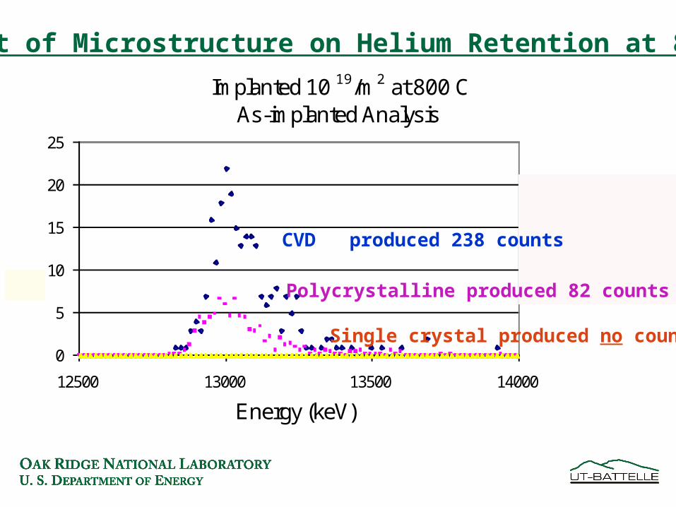
Implanted 10 19/m2 at 800 CAs-implanted Analysis
0
5
10
15
20
25
12500 13000 13500 14000
Energy (keV)
Counts
CVD
Polycrystalline
Single Crystal
Effect of Microstructure on Helium Retention at 800°C
Single crystal produced no counts
Polycrystalline produced 82 counts
CVD produced 238 counts

Observed Area
Single Crystal Tungsten50 x Cyclic RT Implantation/2000°C Anneal
Specimen
1mOver Focus Image
100nm
Under Focus Image
100nm

Under Focus Image
100nm
Larger, resolvable bubbles several nanometers
50 x Cyclic RT Implantation/2000°C Anneal

Summary and Plans for Conclusion of He/W Studies
• Implantation temperature and microstructure have great influence on the diffusion and trapping of helium in tungsten.
• Single crystal (free of grain boundaries, very low impurity) has significantly less retention of materials studied and essentially no retention at IFE relevant temperatures.
• Helium bubbles formed in single crystal following very high temperature annealing are several nanometers in diameter indicating very short diffusion lengths possible confounding “engineered porosity” approach to helium management
Summary

• Complete series of high-temperature implantations and associated TEM to determine controlling microstructural feature. Are grain boundaries or impurities controlling trapping?
• Complete thermal desorption studies. Determine diffusion coefficient of He in W for transport modeling…
• Automate and carry out IFE relevant dose/anneal study on candidate tungsten material. Which material? Chopping?
• Perform degraded energy implantation of He/H. Simulating actual spectrum calculated described by Lucas…
• Results presented/published in MRS winter meeting and ICFRM-11
Concluding Studies

Refractory Armored Silicon Carbide
500
1000
1500
2000
2500
0 2 4 6 8 10Time ( )s
(100 ) Tungsten micron Armor on SiC
- ( ~ 2800° )Non Armored SiC Sublimes at C
Raffray data
• Motivation for this work was to demonstrate at proof-of-principal refractory armored SiC with strong interfacial bonding

Properties of the Plasma Radiant Source
•Maximum lamp power: 35 MW/m2
•Non-contact heating•Rapid heating and cooling•Concentration of heating on surface•Environment: argon, vacuum, air•Three separate plasma heads: 10, 20 and 35 cm arcs•Power delivery: flash mode or scan mode as wide as 35 cm, presently•Lamp power: form 2% to 100% of available radiant output•Change of power levels: less than 20 ms•Wavelength of radiant output: 0.2-1.4 µm•Wavelength: constant and independent of power level and anode/cathode wear

Coating Optimization (Details in Poster Session)
SiC (Hexoloy SA)
Pretreatment*
Brush or spray powder (W or Mo)
IR processing
SiC
*Pretreatment: Ti vapor deposition W or Mo vapor deposition Anneal 72 hours (1300 or 1500ºC)
Vapor deposited Ti
Vapor deposited W or Mo
Anneal
Plasma Arc
Lamp
Specimen size: 25×15×3 (mm)IR processing: uniform irradiance or scan
Flash orscan
W or Mo powder

Effect of Scan Speed on Coating Microstructure
Melted W
Non-melted W
Scan speed: 11.0 mm/sec
5mm
IRHW31
Hexoloy SiC + W (no pretreatment), Lamp power: 23.5 MW/m2
Cross sectional SEM image in middle region
SiC
W coating

Effect of Scan Speed on Coating Microstructure
Melted W
Non-melted W
Scan speed: 10.5 mm/sec
5mm
IRHW32
Hexoloy SiC + W (no pretreatment), Lamp power: 23.5 MW/m2
SiC
W coating
Cross sectional SEM image in middle region

Effect of Scan Speed on Coating Microstructure
Melted W
5mm
IRHW30
Hexoloy SiC + W (no pretreatment), Lamp power: 23.5 MW/m2
Scan speed: 10 mm/sec SiC
W coating
Cross sectional SEM image in middle region
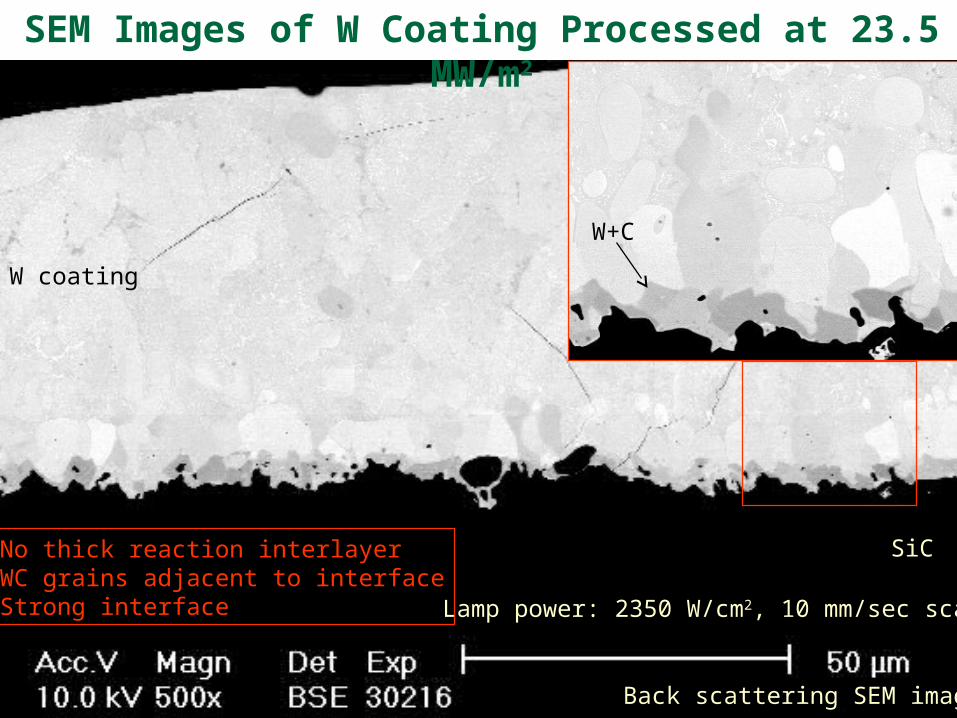
SEM Images of W Coating Processed at 23.5 MW/m2
Lamp power: 2350 W/cm2, 10 mm/sec scan
•No thick reaction interlayer•WC grains adjacent to interface•Strong interface
Back scattering SEM images
W coating
SiC
W+C

100
150
200
250
3 5 7 9 11Scan speed (mm/sec)
Flexural strength (MPa)
Without VDWith VD
Effect of Processing Condition onFlexural Strength of W Coated SiC
W coating side
Four point flexural testSpecimen size: 50x4x3 mmSupport span: 40 mmLoading span: 20 mmCrosshead speed: 10um/sec
Substrate strength
W coating was not peeled off during flexural testStrength of substrate SiC was decreased by IR processingVapor deposition prior to powder coating prevented degradation of strength slightly

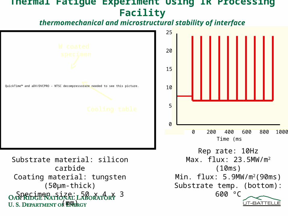
Thermal Fatigue Experiment Using IR Processing Facility
thermomechanical and microstructural stability of interface
Rep rate: 10HzMax. flux: 23.5MW/m2 (10ms)Min. flux: 5.9MW/m2(90ms)Substrate temp. (bottom):
600 ºC
Substrate material: silicon carbideCoating material: tungsten (50µm-
thick)Specimen size: 50 x 4 x 3 (mm)
W coated specimen
Cooling table
0
5
10
15
20
25
-200 0 200 400 600 800 1000Time (ms)
Heat flux (MW/m
2)
W+C

Thermal Fatigue Experiment Using IR Processing Facility
thermomechanical and microstructural stability of interface
Rep rate: 10HzMax. flux: 23.5MW/m2 (10ms)Min. flux: 5.9MW/m2(90ms)Substrate temp. (bottom):
600 ºC
Substrate material: silicon carbideCoating material: tungsten (50µm-
thick)Specimen size: 50 x 4 x 3 (mm)
W coated specimen
Cooling table
0
5
10
15
20
25
-200 0 200 400 600 800 1000Time (ms)
Heat flux (MW/m
2)
QuickTime™ and aDV/DVCPRO - NTSC decompressorare needed to see this picture.

Effect of Thermal Fatigue on Tungsten Coating
Before experiment
After 1000 cycles
Tungsten coating was not peeled off following 1000 cycle thermal fatigue experiments
Rep rate: 10HzMax. flux: 23.5MW/m2 (10ms)Min. flux: 5.9MW/m2(90ms)Cycle: 1000Substrate temp. (bottom): 600 ºC

Mapping “over-cooked” Coating (Higher Power, Slower Scan)
SiC
Wcoating
W
C
SiBack scattering electron image
EDS mappingof W, C, Si
W+C W+Si
Hexoloy SiC + W (no pretreatment)Lamp power: 2350 W/cm2
Scan speed: 9mm/sec
10µm

Summary and Plans for Conclusion of RAC’s
Summary• A fully dense, high-strength tungsten coating has been applied to SiC.• Preliminary thermal fatigue testing shows promise.
Concluding Studies
• What’s required to conclude proof-of-principal?- complete analysis of thermal stability/thermal fatigue of interface- improve uniformity- application to SiC/SiC - results to be published at ICFRM-11

Example from this Conference : N Abe (EPVD)
Good microstructure, though low interfacial strength